Embed Size (px)
Citation preview

Transistor Placement for NoncomplementaryDigital VLSI Cell Synthesis
MICHAEL A. RIEPEMagma Design AutomationandKAREM A. SAKALLAHUniversity of Michign
There is an increasing need in modern VLSI designs for circuits implemented in high-performancelogic families such as Cascode Voltage Switch Logic (CVSL), Pass Transistor Logic (PTL), anddomino CMOS. Circuits designed in these noncomplementary ratioed logic families can be highlyirregular, with complex diffusion sharing and nontrivial routing. Traditional digital cell layoutsynthesis tools derived from the highly stylized “functional cell” style break down when confrontedwith such circuit topologies. These cells require a full-custom, two-dimensional layout style whichcurrently requires skilled manual design. In this work we propose a methodology for the synthesisof such complex noncomplementary digital cell layouts. We describe a new algorithm which permitsthe concurrent optimization of transistor chain placement and the ordering of the transistors withinthese diffusion-sharing chains. The primary mechanism for supporting this concurrent optimiza-tion is the placement of transistor subchains, diffusion-break-free components of the full transistorchains. When a chain is reordered, transistors may move from one subchain (and therefore oneplacement component) to another. We will demonstrate how this permits the chain ordering to beoptimized for both intra-chain and inter-chain routing. We combine our placement algorithms withthird-party routing and compaction tools, and present the results of a series of experiments whichcompare our technique with a commercial cell synthesis tool. These experiments make use of anew set of benchmark circuits which provide a rich sample of representative examples in severalnoncomplementary digital logic families.
Categories and Subject Descriptors: B.6.3 [Logic Design]: Design Aids—Automatic synthesis; B.7.2[Integrated Circuits]: Design Aids—Layout; placement and routing; J.2 [Physical Sciences andEngineering]: Electronics; J.6 [Computer Aided Engineering]: Computer Aided Design (CAD)
General Terms: Algorithms, Design, Experimentation, Performance
Additional Key Words and Phrases: Cell Synthesis, digital circuits, noncomplementary circuits,transistor placement, transistor chaining, Euler graphs, sequence pair optimization, benchmarkcircuits
Work supported by the Defense Advanced Research Projects Agency (DARPA) under ARPA/AROcontract DAAH04-94-G0327.Authors’ addresses: M. A. Riepe, Magma Design Automation, Inc., 2 Results Way, Cuppertino,CA 95014; email: [email protected]; K. A. Sakallah, Department of Electrical Engineering andComputer Science, University of Michigan, 1301 Beal Ave., Ann Arbor, MI 48109-2122; email:[email protected] to make digital/hard copy of part or all of this work for personal or classroom use isgranted without fee provided that the copies are not made or distributed for profit or commercialadvantage, the copyright notice, the title of the publication, and its date appear, and notice is giventhat copying is by permission of ACM, Inc. To copy otherwise, to republish, to post on servers, or toredistribute to lists requires prior specific permission and/or a fee.C© 2003 ACM 1084-4309/03/0100-0081 $5.00
ACM Transactions on Design Automation of Electronic Systems, Vol. 8, No. 1, January 2003, Pages 81–107.

82 • Riepe and Sakallah
1. INTRODUCTION
Library cells are the lowest level of the digital VLSI design hierarchy. Clearly,the quality of cells in a given library has a direct impact on the quality of thefinal design. The cells must be designed to be compact and fast, with minimizedpower and parasitics, and with careful attention paid to requirements on thephysical architecture of the cells as viewed by the higher-level placement androuting tools. Automated synthesis techniques have found limited applicationat the cell level because existing tools are unable to match the quality of humandesigned cells. For this reason cells are often designed by hand, requiring asignificant investment in manpower.
An additional difficulty lies in the fact that the lifetime of a typical cell li-brary may be as short as 1 or 2 years. Compaction techniques may be used tomigrate a cell library to a new process technology if little more than a linearshrink is required, but this is unlikely to extend the lifetime for more than oneor two process generations before the loss in performance necessitates a com-plete redesign of the library. These problems are only becoming worse as devicegeometries shrink into the deep submicron regime.
In order to account for deep submicron effects when designing large chips,ever closer interaction is required between front-end logic synthesis tools andback-end placement and routing tools, power and delay optimization tools,and parasitic extraction tools. In order to enable this interaction, cell librariesmust become more flexible. Multiple versions of each cell with different drivestrengths are required. It may even be necessary to support versions of cellsin different logic families with different power/delay tradeoffs. In leading-edgeintegrated circuit designs, static CMOS and dynamic domino CMOS tend tobe dominant, but there is a growing need for circuits implemented in high-performance logic families such as Cascode Voltage Switch Logic (CVSL) andPass Transistor Logic (PTL). In addition, synchronizing elements such aslatches and flip-flops tend to be designed using custom analog sense amplifiertechniques.
In addition to the need for families of cells which are parameterized in termsof their electrical behavior, it has been demonstrated that standard-cell place-ment and routing tools are able to obtain significantly higher routing quality ifthey have the ability to choose between multiple instances of cells with a widevariety of pin orderings. In one experiment [Lefebvre et al. 1997], an averagereduction in the number of routing tracks of 10.8% was demonstrated over fivebenchmark circuits.
It seems clear that as the number of cells in a typical cell library grows fromthe hundreds into the thousands, a dramatic increase in designer productivitywill be required, necessitating a move toward more automated cell synthesistechniques. Several authors, in fact, advocate a move completely away fromstatic cell libraries as we know them, toward a system which permits the auto-mated synthesis of cells on demand [Lefebvre et al. 1997; Burns and Feldman1998]. This would permit logic synthesis tools to request specific logic decom-positions, doing away with the traditional technology mapping step; standard-cell and datapath placement and routing tools to request cells with an exact pin
ACM Transactions on Design Automation of Electronic Systems, Vol. 8, No. 1, January 2003.

Transfer Placement for Noncomplementary Cell Synthesis • 83
Fig. 1. An example of a complex gate designed in the “functional cell” style of Uehara and Van-Cleemput [1981].
ordering; interconnect optimization tools to request cells with specific input andoutput impedance values; and power optimization tools to request cells, perhapsfrom one of several different logic families, with specific power/delay tradeoffs.
Such an on-demand cell synthesis system will require effort on many fronts:
(1) Automated transistor schematic generation (constraint-driven logic familyselection, netlist creation, and transistor sizing);
(2) automated cell geometry synthesis;(3) automated cell testing and characterization; and(4) development of enabling logic synthesis, placement and routing, and
power/delay optimization technology.
In our work we address the second item in the above list: the fully automaticsynthesis of library cell mask geometry. The input specification consists of asized transistor-level schematic, a process technology description (design rules,parasitics, etc.), and a description of the constraints imposed by the higher-level placement and routing environment. We refer to this last item as thecell template. A list of common cell template constraints are enumerated inLefebvre et al. [1997].
1.1 Motivation
The CMOS cell synthesis problem has a rich history going back approximately20 years. Most of this research has centered on a formulation of the problemwhich was referred to as the “functional cell” in a seminal paper by Uehara andVanCleemput [1981]. In this style, an example of which is given in Figure 1,the transistors take on a very regular row-based structure. They are arrangedin a linear fashion so as to minimize the number of gaps in the diffusion is-lands (so called “diffusion breaks”). We will refer to layouts in this style asone-dimensional, or 1D, layouts.
The synthesis of 1D layouts can be formulated as a straightforward graphoptimization problem: to find a minimal dual Euler-trail covering for a pair of
ACM Transactions on Design Automation of Electronic Systems, Vol. 8, No. 1, January 2003.

84 • Riepe and Sakallah
Fig. 2. A manually designed cell showing complex two-dimensional layout structure.
dual series-parallel multigraphs. Uehara and VanCleemput [1981] developedan approximate solution technique for this problem, while Maziasz and Hayes[1992] presented the first provably optimal algorithms.
A major drawback of the 1D layout style is that it applies directly only tofully complementary nonratioed series-parallel CMOS circuits. Several signif-icant systems have extended this style to cover circuits with limited degreesof irregularity. Among these are C5M [Burns and Feldman 1998], Excellerator[Poirier 1989], LiB [Hsieh et al. 1991], and Picasso II [Lefebvre and Skoll 1992].Dynamic CMOS circuits, if the p-channel pull-up transistors are ignored, canbe optimized using a simpler single-row 1D formulation—a good summary ispresented by Basaran [1997].
Despite the elegant formulation presented by the one-dimensional ab-straction, it must break down at some point. When designing aggressive,high-performance circuits, the designer may call upon logic families such asdomino-CMOS, pseudo-NMOS, CVSL, and PTL. These provide the designerwith different size/power/delay tradeoffs than are available with a static CMOSimplementation. However, these noncomplementary ratioed logic families of-ten result in physical layouts which are distinctly two-dimensional (2D) inappearance.
An example of such a circuit is shown in Figure 2. The example is a hand-designed mux-flip flop standard cell implemented in a complementary GaAsprocess [Bernhardt et al. 1995]. This example demonstrates a number of
ACM Transactions on Design Automation of Electronic Systems, Vol. 8, No. 1, January 2003.

Transfer Placement for Noncomplementary Cell Synthesis • 85
properties which deviate from the standard one-dimensional style:
(1) It is highly irregular. Some regularity is present in the rows, or “chains,”of merged transistors, but these chains are of nonuniform size and are notarranged in two simple rows.
(2) There are instances of complex diffusion sharing, such as the “Z”-shapedstructure in the upper-left corner.
(3) The transistors are given a wide variety of channel widths.(4) The routing is nontrivial.(5) The port structure required by the back end placement and routing tools
must be taken into account.
1.2 Prior Work
A variety of approaches have been taken to address the 2D cell synthesis prob-lem. Tani et al. [1991] and Gupta and Hayes [1997] discussed a style in whichtwo-dimensional layouts are formed from multiple one-dimensional rows. Theformer presented a heuristic technique based on min-cut partitioning whilethe latter presented an exact formulation, called CLIP, based on integer linearprogramming. To distinguish this style from non-row-based two-dimensionalstyles, we refer to it as being 1-1/2 dimensional.
Xia et al. [1994] developed a method for BiCMOS cell generation. The methodgroups MOS transistors into locally optimal chains which behave as fixed blocksin the design. Bipolar transistors are treated individually and are given a fixedarea with a flexible aspect ratio. A branch and bound algorithm is used toexplore a slicing tree-based floorplanning model of the circuit to find a floorplanof minimal area.
It is also relevant to discuss work in analog circuit placement and routingin this context. One such system is Koan/Anagram by Cohn et al. [1994]. Thissystem uses simulated annealing to find a placement of analog components,simultaneously seeking to optimize device connectivity through arbitrary ge-ometry sharing, while satisfying design rule constraints as well as analog con-straints such as device symmetry and matching. It then uses a custom arearouter with aggressive rip-up and reroute capability to make the remainingrequired connections.
Fukui et al. [1995] developed the first system for true two-dimensional digitaltransistor placement and routing. It uses a simulated annealing algorithm tofind good groupings of transistors into diffusion-shared chains and performsa greedy exploration of a slicing structure to find a two-dimensional virtualgrid floorplan. It uses a symbolic router to perform detailed routing, and a finalcompaction step to permit transistors within chains to slide into locally optimalpositions.
In a more recent work by the same group, Saika et al. [1997] pre-sented a second tool which operates by statically grouping the transistorsinto maximally sized series chains and then locating a high-quality one-dimensional solution in order to form more complex chains. Then a simu-lated annealing algorithm is used to modify this linear ordering by placing
ACM Transactions on Design Automation of Electronic Systems, Vol. 8, No. 1, January 2003.

86 • Riepe and Sakallah
the diffusion-connected groups onto a two-dimensional virtual grid. Routing isdone by hand.
Two other efforts which are contemporary with our own [Riepe 1999;Riepe and Sakallah 1999] have recently published results. Vahia, Askar, andCiesielski [Vahia and Ciesielski 1999; Oskar and Ciesielski 1999] describeda fast greedy constructive algorithm for the placement of transistor chains,while Serdar and Sechen [1999] presented an efficient annealing-based solu-tion. Both groups showed very compact layouts of several difficult circuits. How-ever, both limited their search to the placement of statically ordered transistorchains, and both made use of manual routing. In addition both works assumedmultiple layers of metal interconnect, allowing them to work with diffusion-limited placements and thus effectively decoupling the placement and routingproblems.
1.3 Proposed Methodology
In this section we present the architecture for a 2D cell synthesis system whichtargets complex noncomplementary digital MOS circuits. We begin with a pre-cise definition of the problem and then outline the top-level flow in our proposedoptimization methodology.
One can view our problem definition, which is elaborated below, as a relax-ation of the highly stylized rules which were adopted by the 1D “functionalcell” style for the optimization of dual CMOS circuits. Our goal is to attempt toemulate the creativity used by an expert designer by permitting selected newdegrees of freedom in the layout style while keeping the problem of manageablecomplexity.
The following four points summarize our assumptions when defining thecell-level transistor placement and routing problem:
(1) The input to the system is a sized transistor netlist, the process designrules and technology parameters, and a description of the cell layout style(“template constraints”).
(2) Transistor source/drain geometry sharing is encouraged, but is not the pri-mary optimization objective. Obtaining a routed cell of minimum area isthe primary objective.
(3) Individual transistors, or chains of source/drain connected transistors, maybe placed in any position or orientation to optimize the objective as long asthe design rules and template constrains are satisfied.
(4) Routing may be performed in two layers: polysilicon and first-level metal.There is no preferred direction for routing in either layer.
As our top level optimization framework, we adopt the flow diagrammed inFigure 3. In the first step clusters of transistors are formed, each representing aset to be composed into a single merged structure, or transistor chain. Clustersof size one represent degenerate chains of individual transistors. These clustersare passed to the placement step (step 2), where they are assigned a chainordering and broken into diffusion-break free components called subchains, andeach resulting subchain is assigned a position and an orientation. Finally, the
ACM Transactions on Design Automation of Electronic Systems, Vol. 8, No. 1, January 2003.
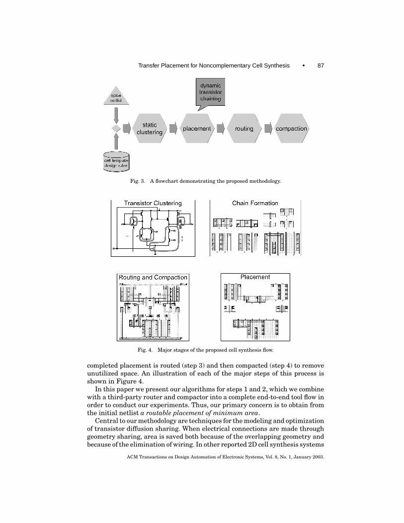
Transfer Placement for Noncomplementary Cell Synthesis • 87
Fig. 3. A flowchart demonstrating the proposed methodology.
Fig. 4. Major stages of the proposed cell synthesis flow.
completed placement is routed (step 3) and then compacted (step 4) to removeunutilized space. An illustration of each of the major steps of this process isshown in Figure 4.
In this paper we present our algorithms for steps 1 and 2, which we combinewith a third-party router and compactor into a complete end-to-end tool flow inorder to conduct our experiments. Thus, our primary concern is to obtain fromthe initial netlist a routable placement of minimum area.
Central to our methodology are techniques for the modeling and optimizationof transistor diffusion sharing. When electrical connections are made throughgeometry sharing, area is saved both because of the overlapping geometry andbecause of the elimination of wiring. In other reported 2D cell synthesis systems
ACM Transactions on Design Automation of Electronic Systems, Vol. 8, No. 1, January 2003.

88 • Riepe and Sakallah
[Xia et al. 1994; Fukui et al. 1995; Saika et al. 1997; Vahia and Ciesielski 1999;Oskar and Ciesielski 1999; Serdar Sechen 1999] this optimization is performedas a static chaining step before placement. Koan [Cohn et al. 1994], which istargeted at analog synthesis, performs no explicit chain formation, but insteadallows arbitrary merged structures to form dynamically during placement.
The unique aspect of our methodology is that it adopts the strengths ofboth the 2D digital cell styles and the analog styles—we make use of a latebinding process in which explicit digital-style transistor chains are optimizeddynamically during placement, and we also allow arbitrary analog-style sharedstructures to form through dynamic geometry merging. During placement thechain optimization process thus has access to global placement and routinginformation which is not available in a static preprocessing step.
1.4 Outline
In the remainder of this paper we elaborate the details of each step in our pro-posed methodology. In Section 2 we review the relevant aspects of transistorchaining theory. In Section 3 we introduce the details of our placement algo-rithms. In Section 4 we discuss the implementation of our experimental system,which is named TEMPO, and present some experimental results. In Section 5we summarize the discussion and provide conclusions.
2. TRANSISTOR CHAINING THEORY
It should be clear from the layout shown in Figure 2 that most geometry sharingin digital circuits, even the complex digital circuits with which we are concerned,takes place within transistor chains. However, in contrast to the functional cellstyle chains of Figure 1, note that the chains in noncomplementary circuits donot normally appear in dual pairs. In this section we review the theory behindnondual transistor chain optimization. We begin by establishing some basicterminology.
Definition 1 (Transistor Cluster). A transistor cluster is an unordered setof same-polarity transistors, all of which are reachable through a sequenceof source or drain terminal connections. These are also often referred to aschannel-connected components (CCCs).
Definition 2 (Transistor Chaining). A transistor chaining is a mappingwhich assigns a unique linear ordering to the source and drain terminals ofthe transistors in a cluster.
Definition 3 (Transistor Chain). A transistor chain is a transistor clusterwhich has been assigned a chaining. This is a well-defined physical structurefor which a design-rule correct layout can be generated.
Definition 4 (Diffusion Break). A diffusion break is a position within atransistor chain at which two neighboring transistors do not share a commonelectrical terminal. Therefore these two terminals will not be able to sharegeometry and must be separated by the proper design rule distance.
ACM Transactions on Design Automation of Electronic Systems, Vol. 8, No. 1, January 2003.

Transfer Placement for Noncomplementary Cell Synthesis • 89
Fig. 5. An example demonstrating our transistor chaining terminology.
Definition 5 (Transistor Subchain). A transistor subchain is a subset of atransistor chain which is free of diffusion breaks. We will make use of thisdefinition in our dynamic chaining approach discussed in Section 3.2.
An example which illustrates the above definitions is provided in Figure 5.Shown is the physical geometry for a single transistor chain with thetransistor gates labeled with letters and the source/drain electrical nodeslabeled with numbers. The example is one possible chaining of the tran-sistor cluster {A, B, C, D, E, F, G, H}. This particular chaining can be de-scribed with the following ordered list of node numbers and gate names:(5, F, 2, B, 1, H, 7, A, 6, 0, E, 4, G, 0, C, 3, D, 0). This chaining consists of twosubchains (5, F, 2, B, 1, H, 7, A, 6) and (0, E, 4, G, 0, C, 3, D, 0), and one diffu-sion break (which can be identified in the ordered chaining list by the presenceof two adjacent node numbers 6, 0).
The process of nondual transistor chain optimization involves two steps.First, the transistors in the design must be partitioned into clusters. Second,a chaining must be found for each cluster. The first problem, transistor clus-tering, has received little attention in the literature and is usually performedheuristically. We will discuss our approach in Section 3.1. The second problem,chain optimization, is traditionally broken up into two components: chain widthminimization and chain height minimization.
Chain width minimization is the process of finding a chaining which mini-mizes the number of diffusion breaks, and hence the width of the chain. Heightminimization is normally the process of locating, from among the set of mini-mum width solutions, a chaining which requires the fewest number of routingtracks to complete the intra-chain source-drain routing.1 However we wouldlike to point out that, while a minimum “height” solution is locally minimalwith respect to the intra-chain routing, it may not be globally minimal withrespect to the complete inter-chain cell routing cost. We will explore this obser-vation more completely in Section 3.2.
Transistor chain width optimization is traditionally posed as a graph prob-lem. An undirected graph called the diffusion graph [Uehara and Van Cleemput1981] is constructed for each cluster by associating a vertex with each electri-cal node. Edges represent transistors and span the corresponding source-drainterminal vertices. A transistor chaining is represented in this graph as a trail
1In the channel routing literature, the required number of routing tracks is often reffered to as themaximum routing density.
ACM Transactions on Design Automation of Electronic Systems, Vol. 8, No. 1, January 2003.

90 • Riepe and Sakallah
Fig. 6. Two different chainings with different maximum routing density.
which traverses every edge exactly once, with a diffusion break occurring be-tween every pair of edges at which the trail is not connected. For example,in Figure 6 we show two different chainings for the same transistor cluster.Both graphs have one diffusion break, but note that chain a requires one fewerhorizontal routing track than chain b and hence has a smaller chain “height.”
An undirected graph which can be covered by a single continuous trail, touch-ing every vertex at least once and every edge exactly once, is called an Euleriangraph, and such a trail is called an Euler trail. It is well known that a graphis Eulerian if and only if it has either zero or two odd-degree vertices. In orderto find a minimum width chaining on a diffusion graph, we use a technique in-troduced by Basaran [1997]. An artificial vertex (the super-vertex) is added andedges (called super-edges) are drawn connecting it to all odd degree vertices,creating an Eulerian graph, which we will call the augmented diffusion graph.The algorithm in Figure 7 is used to find a covering Euler trail on this graph be-ginning at the vertex vα and ending at the vertex vβ . The Euler trail must beginand end at the super-vertex, though any internal vertex may be used if the in-put graph was already Eulerian. The order in which the graph edges are visitedcorresponds to the ordering of the transistors in the chain, with the super-edgescorresponding to diffusion breaks.2 In Figure 6 we show Euler paths associated
2Note that there may be an exponential number of different solutions generated by algorithmEULER, but they will all be optimal in the sense that they all have the same minimal number ofdiffusion breaks
ACM Transactions on Design Automation of Electronic Systems, Vol. 8, No. 1, January 2003.

Transfer Placement for Noncomplementary Cell Synthesis • 91
Fig. 7. Algorithm to locate an Euler path from vα to vβ in an Eulerian graph [Papadimitriou andSteiglitz, 1982].
with each chaining—the augmented diffusion graph super-vertex is labeled “S”and the super-edges are shown with dashed lines.
3. CELL LEVEL TRANSISTOR PLACEMENT
In order to attack the general two-dimensional cell synthesis problem, ourmethodology adopts a very general placement and routing approach. However,the need to optimize diffusion sharing distinguishes this problem from tradi-tional macro-block placement in a number of ways. In the remainder of thissection we discuss our approach to transistor placement. Section 3.1 presentsour algorithm for creation of the static transistor clusters from which we willconstruct our transistor chains. Section 3.2 discusses the algorithms which weuse for the dynamic exploration of the different chainings of each transistorcluster. Section 3.3 discusses a simple method by which we permit more com-plex forms of arbitrary geometry sharing to occur in the placement. Section 3.4shows how these techniques can be combined with a simulated annealing algo-rithm to achieve the concurrent optimization of transistor chain ordering andplacement. Section 3.5 discusses the methods which we use to model the routingcost function during placement.
3.1 Static Transistor Clustering
In the first step, transistor clustering, the goal is to determine the optimalnumber of transistor clusters and which transistors belong in each cluster.However, at this stage very little information is available, only the transistorconnectivity and the sizes of each transistor, so the choices can only be heuristicin nature. On the schematic of the CGaAs mux flip-flop shown in Figure 2,we outline the clusters chosen by the designer in the corresponding manuallayout.
Authors in previous works have used a wide variety of heuristics at thisstage. In Fukui et al. [1995], the authors used simulated annealing. In Saikaet al. [1997], only simple chains made up of maximum length series chains werecreated and larger chains are formed during the 1D optimization step. It is alsofairly common, especially in one-dimensional tools, to approach clustering byperforming logic gate recognition, as in Lefebvre and Skoll [1992].
ACM Transactions on Design Automation of Electronic Systems, Vol. 8, No. 1, January 2003.

92 • Riepe and Sakallah
We begin with an initial set of clusters formed from the set of all maximalchannel-connected components (MCCCs).3 We then make use of a Fidducia-Mattheyses (FM) bipartitioning algorithm [Fiduccia and Mattheyses 1982] torecursively partition these clusters until a user-supplied upper size bound ismet. Because we are primarily interested in minimizing the net cutset, and notin obtaining balanced partitions, a loose balance criterion is used. An optionalfeature allows the user to specify an upper limit on channel width variationamong the transistors in a particular cluster.4 This feature is an alternative totransistor folding, and is enforced when the initial MCCCs are formed.
3.2 Dynamic Transistor Chaining
As we mentioned in Section 3.1, it is very difficult to determine an optimal staticclustering of the transistors into diffusion-connected chains. This is because theclustering step has no information about the relative positions of the chainsin the final placement. For the same reason, traditional chain optimizationalgorithms cannot be expected to locate globally optimal chaining solutions ifperformed as a preprocessing step prior to placement. Such an approach can finda chaining solution with minimum width and minimum internal routing cost(i.e., “height”) but, as mentioned previously, such chainings may not be globallyoptimal when external wiring costs are taken into account. It is thus not cleara priori to which chain a particular transistor should be assigned, and whichchain ordering should be chosen. The following technique, which we refer toas dynamic chain optimization, allows the placement step to dynamically alterthe chainings and thus perform optimization with regard to the global area andwiring costs.
Dynamic chain optimization is enabled by the static clustering step, whichis permitted to find relatively large transistor clusters. Using the algorithmdescribed below, the placement step dynamically explores the universe of allpossible minimum-width chaining solutions for each cluster. For each candi-date chaining solution, a geometry generator is called to obtain the design-rulecorrect chain geometry and perform local intra-chain routing.5 The transistorchains are then split at the diffusion breaks, and the resulting subchains arepassed to the placement engine as the atomic placeable objects. These subchainsare free to be placed in any two-dimensional arrangement that optimizes thearea and the external routing.
It is easy to see that there will be many Euler trail covers for a given cluster’sdiffusion graph, and that all of them will have the same number of diffusionbreaks. Thus the set of all trail covers corresponds to the set of all minimum-width chains, and the number of subchains being placed will remain constant.
3The MCCCs are trivially found in linear time as they are simply the connected components[Cormen et al. 1990] of the diffusion graph.4In the experiments reported in Section 4.3, we use an FM balance criterion tolerance of ±20%,we enforce a maximum cluster size limit of 20 transistors, and we limit the maximum variationamong channel widths to a factor of 2.5Intra-chain routing is a simple instance of one-dimensional routing without vertical constraintsand can be performed optimally in linear time with a greedy left-edge algorithm. This routing isperformed only if full contract strapping is not specified in the cell template.
ACM Transactions on Design Automation of Electronic Systems, Vol. 8, No. 1, January 2003.

Transfer Placement for Noncomplementary Cell Synthesis • 93
Fig. 8. A chain modification performed with Basaran’s [1997] Iterative method.
However, when a new chaining is found for a cluster, individual transistorsmay move from one subchain to another, and the individual subchains maygrow or shrink in size, providing a significant degree of added flexibility duringplacement.
Note again that we are not attempting to optimize the internal routing cost(chain “height”) of the transistor chains, as is traditional in the literature. Infact, the physical height of the chain is fixed by the transistor channel widthsin the input schematic. However, the chain geometry generator will report thenumber of internal chain nets which cannot be routed on top of the chains, andthese nets are added to the global inter-chain routing cost (see Section 3.5).Thus the subchains are optimized such that their internal local routing cost istaken into account as well as the resulting global routing cost.
In our dynamic approach, it is the task of the placement engine to explore theuniverse of all possible minimum-width chainings for each cluster. We make useof the following iterative technique due to Basaran [1997] for generating onevalid chaining from another. As shown in Figure 8, we select a random subtrailfrom the current trail cover and reset the edges of this subtrail in the diffusiongraph. We then call algorithm Euler() to generate a different subtrail with thesame two endpoints. Notice how the relative sizes of the two subchains in ourexample changed as a result of this transformation. By controlling the size of theselected subtrail, one can gain some indirect control over the degree of changeto the chain (a feature which proved useful in implementing the automaticrange limiting capability of our simulated annealing based placement engine).It can be shown that Basaran’s method is complete, and can thus be used toconstruct every possible minimum-width Euler trail which can be embedded inthe selected graph.
3.3 Support for Arbitrary Geometry Sharing
While most geometry sharing in complex cell layouts occurs in explicitly formedtransistor chains, we observed that this is not always the case. An example of
ACM Transactions on Design Automation of Electronic Systems, Vol. 8, No. 1, January 2003.
94 • Riepe and Sakallah
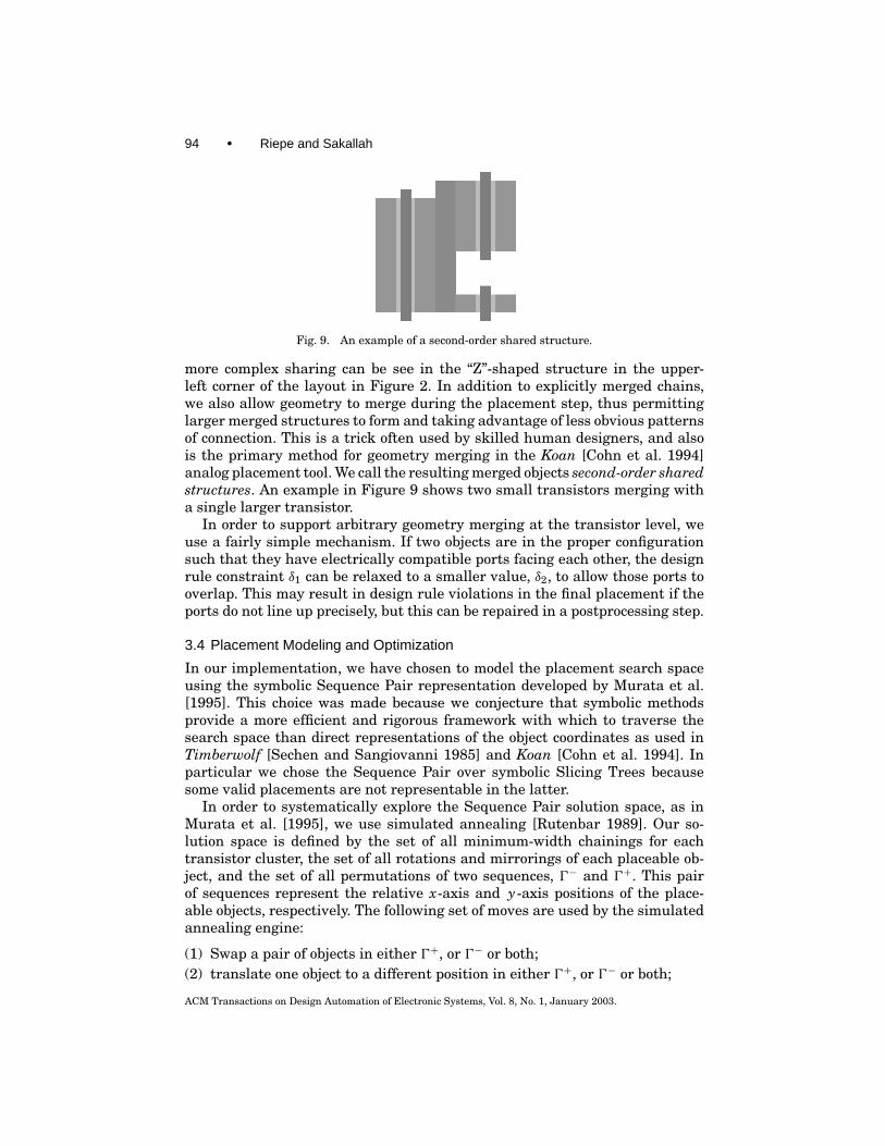
Fig. 9. An example of a second-order shared structure.
more complex sharing can be see in the “Z”-shaped structure in the upper-left corner of the layout in Figure 2. In addition to explicitly merged chains,we also allow geometry to merge during the placement step, thus permittinglarger merged structures to form and taking advantage of less obvious patternsof connection. This is a trick often used by skilled human designers, and alsois the primary method for geometry merging in the Koan [Cohn et al. 1994]analog placement tool. We call the resulting merged objects second-order sharedstructures. An example in Figure 9 shows two small transistors merging witha single larger transistor.
In order to support arbitrary geometry merging at the transistor level, weuse a fairly simple mechanism. If two objects are in the proper configurationsuch that they have electrically compatible ports facing each other, the designrule constraint δ1 can be relaxed to a smaller value, δ2, to allow those ports tooverlap. This may result in design rule violations in the final placement if theports do not line up precisely, but this can be repaired in a postprocessing step.
3.4 Placement Modeling and Optimization
In our implementation, we have chosen to model the placement search spaceusing the symbolic Sequence Pair representation developed by Murata et al.[1995]. This choice was made because we conjecture that symbolic methodsprovide a more efficient and rigorous framework with which to traverse thesearch space than direct representations of the object coordinates as used inTimberwolf [Sechen and Sangiovanni 1985] and Koan [Cohn et al. 1994]. Inparticular we chose the Sequence Pair over symbolic Slicing Trees becausesome valid placements are not representable in the latter.
In order to systematically explore the Sequence Pair solution space, as inMurata et al. [1995], we use simulated annealing [Rutenbar 1989]. Our so-lution space is defined by the set of all minimum-width chainings for eachtransistor cluster, the set of all rotations and mirrorings of each placeable ob-ject, and the set of all permutations of two sequences, 0− and 0+. This pairof sequences represent the relative x-axis and y-axis positions of the place-able objects, respectively. The following set of moves are used by the simulatedannealing engine:
(1) Swap a pair of objects in either 0+, or 0− or both;(2) translate one object to a different position in either 0+, or 0− or both;
ACM Transactions on Design Automation of Electronic Systems, Vol. 8, No. 1, January 2003.

Transfer Placement for Noncomplementary Cell Synthesis • 95
(3) rotate and/or mirror one object into a different orientation; and(4) reorder a selected chain as explained in Section 3.2.
Our simulated annealing engine makes use of a standard adaptive coolingschedule, automated initial temperature selection, range limiting, and statis-tical move selection [Cohn 1992]. The cost function is a weighted combinationof the placement cost and an estimate for the routing cost:
cost = w1 · placement+w2 · routing (1)
Several alternative placement cost metrics can be selected by the user: op-timization of the cell area or perimeter are both possible with the ability tofix the height, width, or aspect ratio. Our routing cost metric is discussed inSection 3.5.
3.5 Routing Model
Because of the serialized split between placement and routing, during the place-ment step we are forced to make use of computationally efficient estimates of theactual routing cost. The routing model which we use during placement accountsfor routing effects in two ways. The routing component of the placement costfunction in Equation (1) is included to encourage the simulated annealing al-gorithm to find a placement, among all near-minimum area placements, whichhas low routing complexity. This cost is estimated with a manhattan net lengthestimate. Multiterminal signal nets are approximated as rectilinear minimumspanning trees (RMSTs), which provide a fairly tight lower bound on the actualrouting cost and can be computed in linear time.6
In addition to the routing complexity component of the cost function, wemust also account for the extra space that this routing will require. Withoutinserting extra space between the transistors prior to routing, we will mostlikely present the router with an infeasible problem, especially when few lay-ers of interconnect are available. However, to model this cost precisely wouldrequire a complete global routing solution. As an alternative, we make use ofthe following approximate technique which is a variant of the technique usedin Murata et al. [1995].
Figure 10(a) shows an intermediate placement without the addition of rout-ing space. It is clear that some nets will be unroutable. Figure 10(b) shows thesame placement with the addition of extra routing space. Here each object istranslated from its original coordinate (xi, yi) to a new coordinate (x ′i, y ′i) basedon an estimate of the total routing resources which will be required below itand to its left. The added boxes demonstrate the movement of each object—the lower-left corner of box i marks (xi, yi) and the upper-right corner marks(x ′i, y ′i), for object i appearing to its upper-right.
6Both Prim’s and Kruskal’s algorithms are O(V + E) where V is number of vertices and E is thenumber of edges.
ACM Transactions on Design Automation of Electronic Systems, Vol. 8, No. 1, January 2003.

96 • Riepe and Sakallah
Fig. 10. A demonstration of routing space insertion.
This cell expansion is performed as follows. We first expand the cell’s bound-ing box using the equation
xmax′ = xmax + βT
∑i∈N
Hi
ymax
, ymax′ = ymax + βT
∑i∈N
Wi
xmax
(2)
where (xmax, ymax) and (xmax′, ymax
′) are the old and new coordinates of theupper-right bounding box corner, respectively, T is the routing pitch, N is theset of all nets, Hi and Wi are the height and width of net i’s bounding box, respec-tively, and β is a user-defined scaling factor.7 We then assign new coordinatesto each block i based on the following equations:
x ′i = xi + (xmax′ − xmax)
xi
xmax, yi
′ = yi + ( ymax′ − ymax)
yi
ymax(3)
This method approximates the total number of horizontal and vertical routingtracks which will be required, assuming that each net requires one horizontaland one vertical track, and distributes these evenly throughout the design. Wetherefore call this the uniform expansion method.8
As a final observation, note that our method does not break apart second-order shared structures (one is marked with an arrow) which are present in theoriginal unexpanded placement. This is explicitly supported in the expansionalgorithm by identifying instances of geometry sharing and assigning all sharedstructures the same expansion factor as the most lower-left shared object.
7In our experiments β was determined experimentally for each circuit by observing the routabilityof several trial placements over a range of different β values.8The method presented in Murata et al. [1995] moves each block based on the set of all routes whichbegin to its lower left. We have found that this places an artificial bias in the routing, concentratingthe routing resources toward the lower left and creating congestion in the upper right. In contrast,our uniform expansion method looks at the total number of required horizontal and vertical routingtracks and obtains the lower-left routing estimate by distributing the required resources evenlythroughout the cell.
ACM Transactions on Design Automation of Electronic Systems, Vol. 8, No. 1, January 2003.

Transfer Placement for Noncomplementary Cell Synthesis • 97
4. EXPERIMENTAL EVALUATION
To validate our approach, we have conducted an extensive series of experimentsusing a new set of high-performance benchmark circuits. In the following wedescribe our prototype implementation and benchmark circuits and report theresults of our experiments.
4.1 Implementation
A prototype tool called TEMPO (Transistor Enabled Micro Placement Opti-mization) has been designed as a framework to explore the ideas discussed inthis paper. TEMPO is implemented in approximately 48,000 lines of C++ codeand has been tested under the Sun Solaris and Linux operating systems. Tocomplete our flow, we make use of the Anagram-II [Cohn et al. 1994] routerfor postplacement detailed routing and the Masterport leaf cell compactor fromCascade Design Automation Inc. We have adopted a datapath-style cell tem-plate for the current set of experiments: Internal routing is assumed to betwo-layer and limited to poly and metal-1. Control inputs are assumed to ar-rive vertically in metal-2 and data/power/ground inputs and outputs arrivehorizontally in metal-3. Prior to routing, we insert these terminals as overcellrouting tracks in a position which is as close as possible to the center of the as-sociated net’s bounding box. Once the detailed routing step has placed contactsto these overcell tracks, the metal geometry is removed, leaving behind a set ofgridded pins for connection by the chip-level router.
4.2 Benchmarks
The lack of a standard set of 2D cell synthesis benchmark circuits has made com-parison with competing approaches difficult. In the case of the static CMOS logicfamily, it is a simple matter to generate artificial benchmark circuits—Maziaszand Hayes [1992], in fact, showed that there are exactly 3505 dual series-parallel circuits of “practical size” (i.e., with a maximum series chain lengthof 4). However, no standard set of circuit benchmarks exist for the broadercategory of circuits with which we are concerned. For the following set of ex-periments, we make use of a new set of 22 benchmark circuits which we haveassembled from the solid-state circuits literature. These circuits, described inTable I, are representative of the class of aggressive, high-performance, andlow-power library cells for which this system is targeted. Included are circuitsdesigned in domino and zipper CMOS, static and dynamic CVSL, as well assingle- and double-ended PTL. As can be seen, these circuits represent a broadcross section of design styles and applications; however, some general obser-vations can be made. Most of the circuits are derived from datapath appli-cations and are either arithmetic circuits, advanced latches and flip-flops, orlatches/flip-flops with embedded logic.
Data which can be used to characterize the complexity of these circuitsis graphed in Figure 11. The circuits range in size from an 18-transistorsense-amp flip-flop to an 84-transistor dynamic eight-way multiplexor takenfrom an experimental 1-GHz PowerPC condition code unit. We also show theaverage net fanout for each circuit as an indication of cell routing complexity
ACM Transactions on Design Automation of Electronic Systems, Vol. 8, No. 1, January 2003.

98 • Riepe and Sakallah
Table I. Benchmark Circuit Descriptions
# Namea Description
1 aoi-lff True Single Phase Clocked Logic (TSPCL) and-or-invert logic flip-flop2 blair-ff High-speed differential double-edge-triggered CMOS flip-flop3 dcsl3-42comp Differential Current Switch Logic 4-2 compressor (DCSL-3 style load)4 dcvsl-xor4 Dynamic Cascode Voltage Switch Logic 4-way XOR gate5 dec-csa-mux High-speed carry-save adder with muxed latching inputs6 diff-fa Differential full adder7 dpl-fa Double-Pass Transistor Logic full adder8 dptl-42comp Dynamic Pass Transistor Logic 4-2 compressor sum logic9 emodl-cla Enhanced Multiple Output Domino Logic carry-lookahead adder stage
10 ghz-ccu-merge 4-Way dynamic merge circuit for 1-GHz PowerPC condition code unit11 ghz-ccu-prop 4-Way dynamic propagate circuit for 1-GHz PowerPC condition code unit12 ghz-mux8-la 8-Input latching mux with hold and scan for 1-GHz PowerPC13 mux2-sdff Semi-Dynamic dual-rail logic flip-flop with embedded 2-input mux14 muxff Dynamic Complementary GaAs mux flip-flop15 ptl-42comp Pass Transistor Logic 4-2 compressor16 ptl-rba Pass Transistor Logic redundant binary adder17 qnp-fa Quasi NP-domino pipelined full adder18 sa-ff Differential edge-triggered sense-amplifier flip-flop19 sa-mux-ff Differential edge-triggered sense-amp flip-flop with embedded 4:1 mux20 t17-fa Seventeen-transistor low-power full-adder21 xor-ff Sense-amplifier flip-flop with dynamic differential embedded XOR gate22 zip-fa2 Dual-bit adder in CMOS zipper logic
aSources: # 1—Rogenmoser and Huang [1996]; # 2—Blair [1997]; 3—Somasekhar and Roy [1996]; # 4—Helleret al. [1984]; # 5—Kowaleski et al. [1996]; # 6—Shimazu et al. [1989]; # 7—Suzuki et al. [1993]; # 8—Hanawaet al. [1996]; # 9—Wang et al. [1997]; # 10—Burns and Nowka [1998]; # 11—Burns and Nowka [1998]; # 12—Silberman et al. [1998]; # 13—Klass [1998]; # 14—Stetson [1997]; # 15—Yano et al. [1996]; # 16—Makino et al.[1996]; # 17—Lu and Samueli [1993]; # 18—Montanero et al. [1996]; # 19—Stephany et al. [1998]; # 20—Shamsand Boyoumi [1998]; # 21—Matsui et al. [1994]; # 22—Friedman and Liu [1984].
(fanout data is shown for all nets, and with the power and ground netsexcluded).
In most cases, the benchmark circuits were specified in the literature withouttransistor sizing information. Due to this fact, and our desire to implementthe circuits in a common technology, we have tuned the transistors in eachcircuit ourselves. We made use of a simple heuristic nonlinear gradient descentalgorithm, described in Riepe [1999], using electrical models from a commercial0.5-µm CMOS process.
In addition to problems in transistor-level layout synthesis, we expectthese benchmarks to prove useful on other problems in high-performance cell-level integrated circuit design automation. Other possible applications includetransistor-level circuit synthesis, transistor tuning, cell testing and character-ization, and performance-driven technology mapping. The characteristics ofthese circuits are described more completely in Riepe [1999], and the sizednetlists can be obtained by contacting the authors.
4.3 Results
We report the results of a series of experiments which compare TEMPO tothe LAS synthesis tool [Chow et al. 1999] from Cadence Design Systems Inc.TEMPO was run on a 300-MHz Intel Pentium-II-based workstation while LASwas run on a 170-MHz Sun Ultrasparc system; both had 128 megabytes of RAM.
ACM Transactions on Design Automation of Electronic Systems, Vol. 8, No. 1, January 2003.

Transfer Placement for Noncomplementary Cell Synthesis • 99
Fig. 11. Benchmark circuit characteristics.
We assume a standard 0.5-mm CMOS process and make use of the MOSISscalable submicron design rules (rev. 7.2) with a lambda value of 0.3 µm. LASwas run in full optimization mode to explore all possible transistor foldingsand cell aspect ratios. It is a 1-1/2-dimensional row-based system which as-sumes a standard-cell style template—to minimize the overhead of the metal-1power rails, we required these to have minimum width. TEMPO cells were op-timized for minimum area under our datapath style cell template. LAS, whichuses deterministic algorithms, was run once per circuit. TEMPO, because ofits stochastic nature, produces results with a statistical spread in quality. Theresults we present for each circuit represent the best solution from a series of100 trials. We discuss runtime, and the statistical distribution of our results,later in this section.
The improvement in benchmark cell area obtained with TEMPO is displayedin Figure 12. The quality of the results is encouraging: with two notable ex-ceptions, the TEMPO layouts are consistently smaller than the LAS layouts.In 15 of the 22 circuits, this improvement exceeded 10%, and in 8 of the 22,
ACM Transactions on Design Automation of Electronic Systems, Vol. 8, No. 1, January 2003.

100 • Riepe and Sakallah
Fig. 12. The cell area improvement seen when comparing TEMPO to LAS.
the improvement exceeded 20%. Three representative layouts are shown inFigure 13. The upper cell is the dcvsl-xor4 benchmark which provides a vi-sually appealing example of a 2D transistor arrangement with fairly sparserouting. This is in contrast to the row-based transistor arrangement and chan-nel routing used by LAS. An area improvement of 39.69% was obtained for thiscircuit. Our second example, the mux2-sdff circuit, provides another demon-stration of dense placement and routing with an area reduction of 18.93%. Ourthird example, the ptl-rba circuit, is one of the two cases for which LAS pro-duced a superior layout. In this case, LAS was able to obtain an extremelyefficient linear transistor arrangement with little wasted space, while TEMPOcould not achieve a competitive placement. In this case, the LAS area is 61.45%smaller than TEMPO’s.
It is interesting to observe the effectiveness of TEMPO’s dynamic geome-try sharing optimization. In Figure 14 we show three different placements ob-tained for the muxff benchmark circuit. In Figure 14(a) we show an optimizedplacement obtained with diffusion sharing disabled—it is obviously extremelynoncompact. In Figure 14(b) we show the pattern of sharing which is obtainedwith our arbitrary geometry sharing mechanism enabled. No explicit transistorchaining is performed in this mode; nevertheless TEMPO is able to discover sev-eral small chains of merged transistors as well as several complex second-ordershared structures. However, the layout is irregular and chain lengths are short,rarely exceeding three or four transistors. This example clearly demonstratesthat digital cells benefit tremendously from an approach based on explicit tran-sistor chain optimization, as seen in the final example in Figure 14(c).
Because TEMPO makes use of a stochastic optimization algorithm, it is likelythat it will achieve a different result every time that it is run. We were interestedin observing the statistical spread in the final layout area obtained in thisway. Figure 15 shows a histogram of the area spread observed for the sa-ffbenchmark. Figure 16 shows the number of standard deviations below the meanat which the minimum area layout was located. This number was consistently
ACM Transactions on Design Automation of Electronic Systems, Vol. 8, No. 1, January 2003.

Transfer Placement for Noncomplementary Cell Synthesis • 101
Fig. 13. Three representative cell layouts. Results of TEMPO are displayed on the left while resultsof LAS are displayed on the right (pairs are shown approximately to scale).
between 1 and 2. Assuming a Gaussian distribution, 95% of the solutions willfall within 2 standard deviations of the mean, indicating that at least 20 trialswill be necessary to achieve good results.
In Figure 17, we show some data indicating the per-run execution timeof TEMPO. Clearly, TEMPO ’s simulated-annealing-based 2D placement algo-rithm, and the Anagram-II router’s aggressive rip-up and reroute strategy, come
ACM Transactions on Design Automation of Electronic Systems, Vol. 8, No. 1, January 2003.

102 • Riepe and Sakallah
Fig. 14. The muxff benchmark (a) without chaining or merging, (b) with chaining disabled, and(c) with both chaining and merging enabled.
Fig. 15. Layout area distribution observed over 100 experimental trials for one representativebenchmark circuit.
at a substantial cost. This cost must also be multiplied by the number of tri-als conducted in the effort to obtain the best layout (100 in our experiments).Improving the convergence behavior and the predictability of the placementresults to eliminate this high cost will be a significant topic of future effort.
5. CONCLUSIONS AND FUTURE WORK
In this work, we have discussed the problem of cell synthesis for high-performance, nondual, digital VLSI cells. Our proposed solution is based on anunconstrained two-dimensional transistor placement and routing framework,
ACM Transactions on Design Automation of Electronic Systems, Vol. 8, No. 1, January 2003.

Transfer Placement for Noncomplementary Cell Synthesis • 103
Fig. 16. Number of standard deviations below the mean at which the minimum area solution foreach benchmark circuit was found.
with an emphasis on methods for the modeling and optimization of geometrysharing among the transistors. Our specific contributions include the following:
(1) A static transistor clustering technique, consisting of an FM-style bipar-titioning algorithm with a loose balance criterion and an optional upperbound on transistor channel width variation.
(2) A simulated annealing placement optimization engine with a new degreeof freedom: dynamic transistor chain optimization. This late-binding tech-nique allows chain optimization to proceed with detailed knowledge of theglobal placement and routing cost function.
(3) A unique placement model in which the atomic placeable objects consist oftransistor subchains. As new chainings are found for each cluster duringplacement, transistors may move from one subchain in the cluster to an-other, and the relative sizes of the subchains may change, but the numberof subchains (and thus placeable objects) remains constant.
(4) Support for the sharing of geometry between arbitrary neighboring objectsin the placement.
(5) A routing component in the placement cost function which includes tran-sistor subchain “spill” routing, as well as global inter-chain routing costestimates, permitting global routing costs to be optimized.
(6) A new variant of an algorithm for the insertion of routing space in theplacement cost function.
(7) A new set of 22 benchmark circuits representing leafcells in a wide varietyof noncomplementary digital logic families.
We have developed a prototype implementation of a transistor-level place-ment tool based on these ideas, and assembled a complete end-to-end synthesisflow which makes use of third-party tools for detailed routing and postroutingcompaction. An initial set of experiments, conducted on a new set of bench-mark circuits, demonstrated encouraging results. However, the wide statistical
ACM Transactions on Design Automation of Electronic Systems, Vol. 8, No. 1, January 2003.

104 • Riepe and Sakallah
Fig. 17. TEMPO and LAS run time statistics for all 22 benchmark circuits. Times shown are for asingle run of each tool. To account for statistical spread, TEMPO was run 100 times on each circuitand the best result reported.
spread in the quality of results produced by our stochastic placement opti-mization approach resulted in a high computational cost which will need to beremedied in the future.
Our experience has demonstrated a number of promising areas for improve-ment and further work. Currently we make no effort to maintain symmetry be-tween transistor chains, since we are not targeting series-parallel CMOS logicfamilies. However, series-parallel subcircuits are often embedded within largercircuits, so it would be beneficial to include some form of dual-chain optimiza-tion capability as well. In addition, in order to simplify poly gate routing, it willoften be advantageous to maintain partial symmetry between chains, dual ornot, which share many common gate inputs. Some logic families, most notably
ACM Transactions on Design Automation of Electronic Systems, Vol. 8, No. 1, January 2003.

Transfer Placement for Noncomplementary Cell Synthesis • 105
CVSL, contain sensitive analog circuitry which requires symmetric placementand routing capability, and techniques for this could be borrowed from the ana-log placement and routing literature. We also see the need for parasitic-awareperformance-driven optimization techniques, transistor folding support, opti-mized well and well contact insertion, and more accurate techniques for routingcost estimation and congestion management.
ACKNOWLEDGMENTS
The authors would like to thank Professor Rob Rutenbar and Dr. PhirozeParakh for many interesting discussions, and the anonymous reviewers fortheir helpful suggestions.
REFERENCES
ASKAR, S. AND CIESIELSKI, M. 1999. Analytical approach to custom datapath design. In Proceedingsof the 1999 International Conference on Computer-Aided Design. 98–101.
BASARAN, B. 1997. Optimal diffusion sharing in digital and analog CMOS layout. Ph.D. dis-sertation, Carnegie Mellon University, Pittsburgh, PA; also, CMU Report No. CMUCAD-97-21,Carnegie Mellon University, Pittsburgh, PA.
BERNHARDT, B. ET AL. 1995. Complementary GaAs (CGaAsTM): A high performance BiCMOS al-ternative. In Proceedings of the 1995 GaAs IC Symposium. 18–21.
BLAIR, G. 1997. Comments on “New single-clock CMOS latches and flip-flops with improvedspeed and power savings.” IEEE J. Solid State Circ. 32, 10 (Oct.), 1611.
BURNS, J. AND FELDMAN, J. 1988. C5M—a control logic layout synthesis system for high-performance microprocessors. IEEE Trans. CAD 17, 1 (Jan.), 14–23.
BURNS, J. AND NOWKA, K. 1998. Parallel condition-code generation for high-frequency powerPCmicroprocessors. In Proceedings of the 1998 Symposiums on VLSI Circuits. 115.
CHOW, S., CHANG, H., LAM, J., AND LIAO, Y. 1992. The layout synthesizer: An automatic blockgeneration system. In Proceedings of the 1992 CICC. 11.1.1–11.1.4.
COHN, J. 1992. Automatic device placement for analog cells in KOAN. Ph.D. dissertation,Carnegie Mellon University, Pittsburgh, PA; also, CMU Report No. CMUCAD-92-07, CarnegieMellon University, Pittsburgh, PA.
COHN, J., GARROD, D., RUTENBAR, R., AND CARLEY, L. R. 1994. Analog Device-Level Layout Automa-tion. Kluwer Academic Publishers, Boston, MA.
CORMEN, T., LEISERSON, C., AND RIVEST, R. 1990. Introduction to Algorithms. McGraw-Hill BookCompany, New York, NY. 88.
FIDUCCIA, C. AND MATTHEYSES, R. 1982. A linear-time heuristic for improving network partitions.In Proceedings of the 19th Design Automation Conference. 241–247.
FRIEDMAN, V. AND LIU, S. 1984. Dynamic logic CMOS circuits. IEEE J. Solid State Circ. 19, 2(Apr.), 265.
FUKUI, M., SHINOMIYA, N., AND AKINO, T. 1995. A new layout synthesis for leaf cell design. InProceedings of the 1995 ASP Design Automation Conference. 259–263.
GUPTA, A. AND HAYES, J. P. 1997. CLIP: An optimizing layout generator for two-dimensional CMOScells. In Proceedings of the 34th Design Automation Conference. 452–455.
HANAWA, M., KANEKO, K., KAWASHIMO, T., AND MARUYAMA, H. 1996. A 4.3ns 0.3mm CMOS 54x54bmultiplier using precharged pass-transistor logic. In Proceedings of the 1996 International Solid-State Circuits Conference. 265.
HELLER, L., GRIFFIN, W., DAVIS J., AND THOMAS, N. 1984. Cascode voltage switch logic: A differentialCMOS logic family. In Proceedings of the 1984 International Solid-State Circuits Conference. 17.
HSIEH, Y., HUANG, C., LIN, Y., AND HSU, Y. 1991. LiB: A CMOS cell compiler. IEEE Trans. Comput.-Aided Des. 10, 8 (Aug.), 994–1005.
KLASS, F. 1998. “Semi-dynamic and dynamic flip-flops with embedded logic. In Proceedings ofthe 1998 Symposium VLSI Ciruits. 109.
ACM Transactions on Design Automation of Electronic Systems, Vol. 8, No. 1, January 2003.

106 • Riepe and Sakallah
KOWALESKI, J., WOLRICH, G., FISCHER, T., DUPCAK, R., KROESEN, P., PHAM, T., AND OLESIN, A. 1996. Adual-execution pipelined floating-point CMOS processor. In Proceedings of the 1996 InternationalSolid-State Circuits Conference. 359.
LEFEBVRE, M. AND SKOLL, D. 1992. PicassoII: A CMOS leaf cell synthesis system. In Proceedingsof the 1992 MCNC International Workshop on Layout Synthesis, vol. 2. 207–219.
LEFEBVRE, M., MARPLE, D., AND SECHEN, C. 1997. The future of custom cell generation in physicalsynthesis. In Proceedings of the 1997 Design Automation Conference. 446–451.
LU, F. AND SAMUELI, H. 1993. A 200-MHz CMOS pipelined multiplier-accumulator using a quasi-domino dynamic full-adder cell design. IEEE J. Solid State Circ. 28, 2 (Feb.), 125.
MAKINO, H., SUZUKI, H., MORINAKA, H., NAKASE, Y., MASHIKO, K., AND SUMI, T. 1996. A 286 MHz64-b floating point multiplier with enhanced CG operation. IEEE J. Solid State Circ. 31, 4 (April),510.
MATSUI, M., HARA, H., UETANI, Y., KIM, L.-S., NAGAMATSU, T., WATANABI, Y., CHIBA, A., MATSUDA, K.,AND SAKURAI, T. 1994. A 200 MHz 13 mm2 2-D DCT macrocell using sense-amplifying pipelineflip-flop scheme. IEEE J. Solid State Circ. 29, 12 (Dec.), 1484.
MAZIASZ, R. L. AND HAYES, J. P. 1992. Layout Minimization of CMOS Cells. Kluwer AcademicPublishers, Boston, MA.
MONTANERO, J., WITEK, R., ANNE, K., BLACK, A., COOPER, E., DOBBERPUHL, D., DONAHUE, P., ENO, J.,FARELL, A., HOEPPNER, G., KRUCKEMYER, D., LEE, T., LIN, P., MADDEN, L., MURRAY, D., PEARCE, M.,SANTHANAM, S., SNYDER, K., STEPHANY, R., AND THIERAUF, S. 1996. A 160 MHz 32b 0.5 W CMOSRISC microprocessor. In Proceedings of the 1996 International Solid-State Circuits Conference.215.
MURATA, H., FUJIYOSHI, K., NAKATAKE, S., AND KAJITANI, Y. 1995. Rectangle packing based moduleplacement. In Proceedings of the 1995 International Conference on Computer-Aided Design. 472–479.
PAPADIMITRIOU, C. AND STEIGLITZ, K. 1982. Combinatorial optimization algorithms and complexity.Prentice-Hall, Englewood Cliffs, NJ. 413.
POIRIER, C. 1989. Excellerator: Custom CMOS leaf cell layout generator. IEEE Trans. Comput.-Aided Des. 8 (July), 744–755.
RIEPE, M. AND SAKALLAH, K. 1999. Transistor-level micro-placement and routing for two-dimensional digital VLSI cell synthesis. In Proceedings of the 1999 International Symposiumon Physical Design. 74–81.
RIEPE, M. 1999. Transistor-level micro-placement and routing for two-dimensional digital VLSIcell synthesis. Ph.D dissertation, The University of Michigan, Ann Arbor, MI.
ROGENMOSER, R. AND HUANG, Q. 1996. An 800-MHz 1-µm CMOS pipelined 8-b adder using truesingle-phase clocked logic-flip-flops. IEEE J. Solid State Circ. 31, 3 (Mar.), 405.
RUTENBAR, R. 1989. Simulated annealing algorithms: An overview. IEEE Circ. Dev. 5, 1 (Jan.)19–26.
SAIKA, S., FUKUI, M., SHINOMIYA, N., AND AKINO, T. 1997. A two-dimensional transistor placementalgorithm for cell synthesis and its application to standard cells. IEICE Trans. Fund., E80–A, 10(Oct.), 1883–1891.
SECHEN, C. AND SANGIOVANNI-VINCENTELLI, A. 1985. The TimberWolf placement and routing pack-age. IEEE J. Solid State Circ. SC-20, 2 (Apr.), 510–522.
SERDAR, T. AND SECHEN, C. 1999. AKORD: Transistor level and mixed transistor/gate level place-ment tool for digital datapaths. In Proceedings of the 1999 International Conference on Computer-Aided Design. 91–97.
SHAMS, A. AND BAYOUMI, M. 1998. A new full adder cell for low-power applications. In Proceedingsof the 1998 Great Lakes Symposium on VLSI. 47.
SHIMAZU, Y., KENGAKU, T., FUJIYAMA, T., TERAOKA, E., OHNO, T., TOKUDA, T., TOMISAWA, O., AND TSUJIMICHI,S. 1989. A 50MHz 24b floating-point DSP. In Proceedings of the 1996 International Solid-StateCircuits Conference. 45.
SILBERMAN, J., AOKI, N., BOERSTLER, D., BURNS, J., DHONG, S., ESSBAUM, A., GHOSAL, U., HEIDEL, D.,HOFSTEE, P., LEE, K., MELTZER, D., NGO, H., NOWKA, K., POSLUSZNY, S., TAKAHASHI, O., VO, I., AND
ZORIC, B. 1998. A 1.0GHz single-issue 64b PowerPC integer processor. In Proceedings of the1998 International Solid-State Circuits Conference. p. 231.
ACM Transactions on Design Automation of Electronic Systems, Vol. 8, No. 1, January 2003.

Transfer Placement for Noncomplementary Cell Synthesis • 107
SOMASEKHAR, D. AND ROY, K. 1996. Differential current switch logic: A low power DCVS logicfamily. IEEE J. Solid State Circ. 31, 7 (July), 987.
STEPHANY, R., ANNE, K., BELL, J., CHENEY, G., ENO, J., HOEPPNER, G., JOE, G., KAYE, R., LEAR, J., LITCH,T., MEYER, J., MONTANARO, J., PATTON, K., PHAM, T., REIS, R., SILLA, M., SLATON, J., SNYDER, K., AND
WITEK, R. 1998. A 200 MHz 32b 0.5 W CMOS RISC microprocessor. In Proceedings of the 1998International Solid-State Circuits Conference. 239.
STETSON, S. 1997. University of Michigan, Ann Arbor, MI. Private communication.SUZUKI, M., OHKUBO, N., YAMANAKA, T., SHIMIZU, A., AND SASAKI, K. 1993. A 1.5ns 32b CMOS ALU
in double pass-transistor logic. In Proceedings of the 1993 International Solid-State CircuitsConference. 91.
TANI, K. ET AL. 1991. Two-dimensional layout synthesis for large-scale CMOS circuits. In Pro-ceedings of the 1991 International Conference on Computer-Aided Design. 490–493.
UEHARA, T. AND VANCLEEMPUT, W. M. 1981. Optimal layout of CMOS functional arrays. IEEETrans. Comput. C-30, 5 (May), 305–312.
VAHIA, D. AND CIESIELSKI, M. 1999. Transistor level placement for full custom datapath cell design.In Proceedings of the 1999 International Symposium on Physical Design. 158–163.
WANG, Z., JULLIEN, G., MILLER, W., WANG, J., AND BIZZAN, S. 1997. Fast Adders Using EnhancedMultiple-Out-put Domino Logic. IEEE J. Solid State Circ. 32, 2 (Feb.), 209.
XIA, H., LEFEBVRE, M., AND VINKE, D. 1994. Optimization-based placement algorithm for BiCMOSleaf cell generation. IEEE J. Solid State Circ. 29, 10 (Oct.), 1227–1237.
YANO, K., SASAKI, Y., RIKINO, K., AND SEKI, K. 1996. Top-down pass-transistor logic design. IEEEJ. Solid State Circ. 31, 6 (June), 797.
Received December 2000; accepted March 2002
ACM Transactions on Design Automation of Electronic Systems, Vol. 8, No. 1, January 2003.