Embed Size (px)
Citation preview

4. CMOS Transistor Theory
Jacob Abraham
Department of Electrical and Computer EngineeringThe University of Texas at Austin
VLSI DesignFall 2019
September 10, 2019
ECE Department, University of Texas at Austin Lecture 4. CMOS Transistor Theory Jacob Abraham, September 10, 2019 1 / 31

Electrical Properties
Necessary to understand basic electrical properties of the MOStransistor to design useful circuits
Deal with non-ideal devices
Ensure that the circuits are robust
Create working layouts
Predict delays and power consumption
As circuit dimensionsscale down, electricaleffects become moreimportant, even fordigital circuits
1.65 GHz square wavefrom an HDMI Interface
(Source: Dunnihoo, EE
Times Asia, 8/25/2005)
ECE Department, University of Texas at Austin Lecture 4. CMOS Transistor Theory Jacob Abraham, September 10, 2019 1 / 31

The nMOS Transistor
Terminal Voltages
Modes of operation depend on Vg, Vd, VsVgs = Vg − VsVgd = Vg − VdVds = Vd − Vs = Vgs − Vgd
Source and drain are symmetric diffusion terminals
By convention, source is terminal at lower voltage, so Vds ≥ 0
nMOS body is grounded for simple designs; assume source is 0
Three regions of operation: Cutoff, Linear, Saturated
ECE Department, University of Texas at Austin Lecture 4. CMOS Transistor Theory Jacob Abraham, September 10, 2019 2 / 31
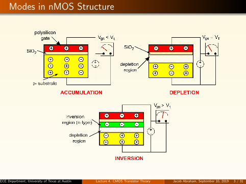
Modes in nMOS Structure
ECE Department, University of Texas at Austin Lecture 4. CMOS Transistor Theory Jacob Abraham, September 10, 2019 3 / 31

nMOS Transistor Operation
Positive voltage on Gate produces electric field across substrate –attracts electrons to the Gate and repels holes
With sufficient voltage, region under Gate changes from p- ton-Type – conducting path between the Source and Drain
Inversion layer is field-induced junction, unlike a PN junctionwhich is metallurgical
Horizontal component of electric field associated with Vds > 0is responsible for sweeping electrons from channel to drain
Threshold Voltage
The gate voltage at which conduction takes place is theThreshold Voltage, Vt
Current flow occurs when the drain to source voltage Vds > 0,and consists almost entirely of majority-carriers (electrons),that flow through the channel
A depletion region insulates the channel from the substrateECE Department, University of Texas at Austin Lecture 4. CMOS Transistor Theory Jacob Abraham, September 10, 2019 4 / 31

Conducting nMOS Transistor
Conduction when Vgs > Vt and Vds > 0No significant current through the substrate because of reversebiased PN junction with the channelAs the voltage from drain to source is increased, the resistivedrop along the channel begins to change the shape of thechannel characteristicAt source end of the channel, the full gate voltage is effectivein inverting the channelAt drain end of the channel, only the difference between thegate and the drain voltage is effective
If Vds > Vgs − Vt, then Vgd < Vt, and the channel is “pincheddown” (the inversion layer no longer reaches the drain)
In this case, conduction is brought about by the driftmechanism of electrons under the influence of positive drainvoltage; as the negative electrons leave the channel, they areaccelerated towards the drain
Voltage across the pinchdown channel tends to remain fixedat (Vgs − Vt), and the channel current remains constant withincreasing Vds
ECE Department, University of Texas at Austin Lecture 4. CMOS Transistor Theory Jacob Abraham, September 10, 2019 5 / 31

nMOS Device Behavior
Vgs > Vt, Vds = 0
Saturated Mode(Vds > Vgs − Vt)
Nonsaturated ModeVds < Vgs − Vt
ECE Department, University of Texas at Austin Lecture 4. CMOS Transistor Theory Jacob Abraham, September 10, 2019 6 / 31

The pMOS Transistor
Moderately doped n- typesubstrate (or well) in whichtwo heavily doped p+ regions,the Source and Drain, arediffused
Application of a negative gate voltage (w.r.t. source) drawsholes into the region below the gate; channel changes from nto p-type (source-drain conduction path)
Conduction due to holes; negative Vd sweeps holes fromsource (through channel) to drain
ECE Department, University of Texas at Austin Lecture 4. CMOS Transistor Theory Jacob Abraham, September 10, 2019 7 / 31
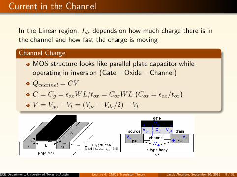
Current in the Channel
In the Linear region, Ids depends on how much charge there is inthe channel and how fast the charge is moving
Channel Charge
MOS structure looks like parallel plate capacitor whileoperating in inversion (Gate – Oxide – Channel)
Qchannel = CV
C = Cg = εoxWL/tox = CoxWL (Cox = εox/tox)
V = Vgc − Vt = (Vgs − Vds/2)− Vt
ECE Department, University of Texas at Austin Lecture 4. CMOS Transistor Theory Jacob Abraham, September 10, 2019 8 / 31

Carrier Velocity
Charge is carried by electrons
Carrier velocity ν proportional to lateral E- field betweensource and drain
ν = µE
µ is called mobility
E = Vds/L
Time for carrier to cross channel: t = L/ν
ECE Department, University of Texas at Austin Lecture 4. CMOS Transistor Theory Jacob Abraham, September 10, 2019 9 / 31

I-V Characteristics
nMOS Linear I-V
Current can be obtained from charge in channel and the time teach carrier takes to cross
Ids =Qchannel
t
= µCoxW
L(Vgs − Vt − Vds/2)Vds
= β (Vgs − Vt − Vds/2)Vds
nMOS Saturation I-V
If Vgd < Vt, channel pinches off near drain
when Vds > Vdsat = Vgs − VtNow drain voltage no longer increases with current
Ids = β (Vgs − Vt − Vdsat/2)Vdsat
=β
2(Vgs − Vt)2
ECE Department, University of Texas at Austin Lecture 4. CMOS Transistor Theory Jacob Abraham, September 10, 2019 10 / 31

nMOS I-V Summary
Shockley First Order transistor models
Ids =
0 Vgs < Vt Cutoff
β (Vgs − Vt − Vds/2)Vds Vds < Vdsat Linearβ2 (Vgs − Vt)2 Vds > Vdsat Saturation
ECE Department, University of Texas at Austin Lecture 4. CMOS Transistor Theory Jacob Abraham, September 10, 2019 11 / 31

pMOS I-V
All dopings and voltages are inverted for pMOS (compared withnMOS)
Mobility µp is determined by holes
Typically 2x-3x lower than that of electrons µn
Thus pMOS must be wider to provide the same current
Simple assumption, µn
µp= 2
ECE Department, University of Texas at Austin Lecture 4. CMOS Transistor Theory Jacob Abraham, September 10, 2019 12 / 31
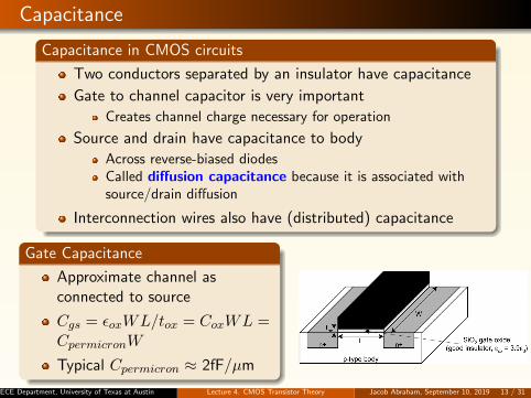
Capacitance
Capacitance in CMOS circuits
Two conductors separated by an insulator have capacitance
Gate to channel capacitor is very important
Creates channel charge necessary for operation
Source and drain have capacitance to body
Across reverse-biased diodesCalled diffusion capacitance because it is associated withsource/drain diffusion
Interconnection wires also have (distributed) capacitance
Gate Capacitance
Approximate channel asconnected to source
Cgs = εoxWL/tox = CoxWL =CpermicronW
Typical Cpermicron ≈ 2fF/µm
ECE Department, University of Texas at Austin Lecture 4. CMOS Transistor Theory Jacob Abraham, September 10, 2019 13 / 31
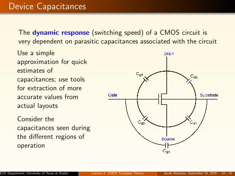
Device Capacitances
The dynamic response (switching speed) of a CMOS circuit isvery dependent on parasitic capacitances associated with the circuit
Use a simpleapproximation for quickestimates ofcapacitances; use toolsfor extraction of moreaccurate values fromactual layouts
Consider thecapacitances seen duringthe different regions ofoperation
ECE Department, University of Texas at Austin Lecture 4. CMOS Transistor Theory Jacob Abraham, September 10, 2019 14 / 31

Device Capacitances, Cont’d
Off Region
Vgs ≤ Vt; when the MOS device is off, only Cgb (due to theseries combination of gate oxide and depletion layercapacitance) is non-zero.
Cgb = Cox = εA/tox, where A is the gate area, andε = ε0εSiO2
ε0 is the permittivity of free space (8.854× 10⁴ F/m), andεSiO2
is the dielectric constant of SiO2 (about 3.9)
Linear Region
Depletion region exists, forming dielectric of depletioncapacitance, Cdep in series with Cox
As the device turns on, Cgb reduces to 0
The gate capacitance is now a function of the gate voltage
ECE Department, University of Texas at Austin Lecture 4. CMOS Transistor Theory Jacob Abraham, September 10, 2019 15 / 31
Device Capacitances, Cont’d
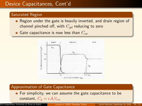
Saturated Region
Region under the gate is heavily inverted, and drain region ofchannel pinched off, with Cgd reducing to zero
Gate capacitance is now less than Cox
Approximation of Gate Capacitance
For simplicity, we can assume the gate capacitance to beconstant, Cg = εA/tox
ECE Department, University of Texas at Austin Lecture 4. CMOS Transistor Theory Jacob Abraham, September 10, 2019 16 / 31
Source: Mlynik and Leblebici
EPFL web-based course

Diffusion (Source/Drain) Capacitance
Capacitance at the drain (Cdb) orsource (Csb) of a device, or whendiffusion is used as a wire
Two components:
1 An Area component
2 A Peripheral (sidewall)component
The peripheral component comesfrom the depth of the diffusion
Assume diffusioncapacitance isapproximately Cg forcontacted diffusion
It is 1/2Cg foruncontacted diffusion
ECE Department, University of Texas at Austin Lecture 4. CMOS Transistor Theory Jacob Abraham, September 10, 2019 17 / 31
Contacted Uncontacted
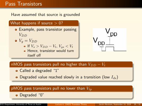
Pass Transistors
Have assumed that source is grounded
What happens if source > 0?
Example, pass transistor passingVDDVg = VDD
If Vs > VDD − Vt, Vgs < VtHence, transistor would turnitself off
nMOS pass transistors pull no higher than VDD − VtCalled a degraded “1”
Degraded value reached slowly in a transition (low Ids)
pMOS pass transistors pull no lower than Vtp
Degraded “0”
ECE Department, University of Texas at Austin Lecture 4. CMOS Transistor Theory Jacob Abraham, September 10, 2019 18 / 31

Pass Transistor Circuits
What would be the voltages on the different nodes?
ECE Department, University of Texas at Austin Lecture 4. CMOS Transistor Theory Jacob Abraham, September 10, 2019 19 / 31

Pass Transistor Circuits
What would be the voltages on the different nodes?
ECE Department, University of Texas at Austin Lecture 4. CMOS Transistor Theory Jacob Abraham, September 10, 2019 20 / 31

Pass Transistor Circuits
What would be the voltages on the different nodes?
ECE Department, University of Texas at Austin Lecture 4. CMOS Transistor Theory Jacob Abraham, September 10, 2019 21 / 31

Example 1
Assumption: initial voltage on each node is 2.5 volts
Relevant transistor parameters are, Vdd = 5V , Vtn = 1V and|Vtp| = 0.7V
ECE Department, University of Texas at Austin Lecture 4. CMOS Transistor Theory Jacob Abraham, September 10, 2019 22 / 31
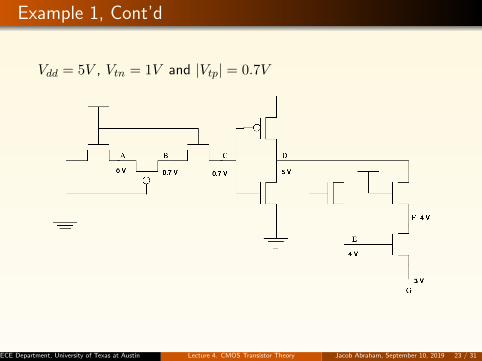
Example 1, Cont’d
Vdd = 5V , Vtn = 1V and |Vtp| = 0.7V
ECE Department, University of Texas at Austin Lecture 4. CMOS Transistor Theory Jacob Abraham, September 10, 2019 23 / 31
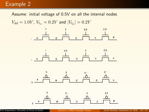
Example 2
Assume: initial voltage of 0.5V on all the internal nodes
Vdd = 1.0V , Vtn = 0.2V and |Vtp | = 0.2V
ECE Department, University of Texas at Austin Lecture 4. CMOS Transistor Theory Jacob Abraham, September 10, 2019 24 / 31

Example 2, Cont’d
Assume: initial voltage of 0.5V on all the internal nodes
Vdd = 1.0V , Vtn = 0.2V and |Vtp | = 0.2V
ECE Department, University of Texas at Austin Lecture 4. CMOS Transistor Theory Jacob Abraham, September 10, 2019 25 / 31

Effective Resistance
Resistance of a bar of uniform material
R = ρ×LA =
(ρt
) (LW
)where ρ = resistivity of the materialA = cross-section of the resistort,W = thickness, width of the material
The channel resistance of a MOS transistor in the linearregion, Rc = k
(LW
),
where k = 1µCox(Vgs−Vt)
Resistance values depend on the technology
Obtain the information from the technology files
Sheet resistance (Ω/)Lowest for metal, increases for poly, active, highest for Well
Contact (via) resistance becomes more important asprocesses scale down
Channel (turned-on transistor) on the order of 1000 Ω/
ECE Department, University of Texas at Austin Lecture 4. CMOS Transistor Theory Jacob Abraham, September 10, 2019 26 / 31

Example of Process Parameters and Simulation
Example: TSMC 0.18µ process
http://www.europractice-ic.com/technologies TSMC.php
Look at one process
Example of SPICE simulation
ECE Department, University of Texas at Austin Lecture 4. CMOS Transistor Theory Jacob Abraham, September 10, 2019 27 / 31
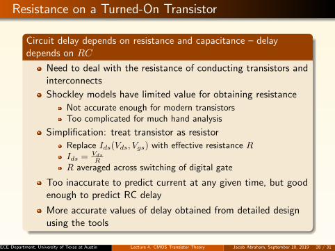
Resistance on a Turned-On Transistor
Circuit delay depends on resistance and capacitance – delaydepends on RC
Need to deal with the resistance of conducting transistors andinterconnects
Shockley models have limited value for obtaining resistance
Not accurate enough for modern transistorsToo complicated for much hand analysis
Simplification: treat transistor as resistor
Replace Ids(Vds, Vgs) with effective resistance RIds = Vds
RR averaged across switching of digital gate
Too inaccurate to predict current at any given time, but goodenough to predict RC delay
More accurate values of delay obtained from detailed designusing the tools
ECE Department, University of Texas at Austin Lecture 4. CMOS Transistor Theory Jacob Abraham, September 10, 2019 28 / 31

RC Delay Model
Use equivalent circuits for MOS transistors
Ideal switch + capacitance and ON resistance
Unit nMOS has resistance R, capacitance CUnit pMOS has resistance 2R, capacitance C
Capacitance proportional to width
Resistance inversely proportional to width
ECE Department, University of Texas at Austin Lecture 4. CMOS Transistor Theory Jacob Abraham, September 10, 2019 29 / 31

Inverter Delay Estimate
Estimate the delay of a fanout-of-1 inverter
d = 6RC
ECE Department, University of Texas at Austin Lecture 4. CMOS Transistor Theory Jacob Abraham, September 10, 2019 30 / 31

Inverter Delay Estimate
Estimate the delay of a fanout-of-1 inverter
d = 6RC
ECE Department, University of Texas at Austin Lecture 4. CMOS Transistor Theory Jacob Abraham, September 10, 2019 30 / 31

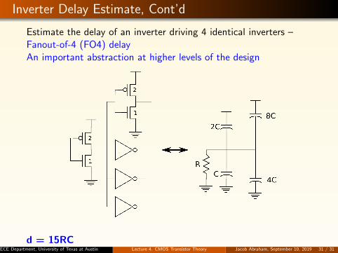
Inverter Delay Estimate, Cont’d
Estimate the delay of an inverter driving 4 identical inverters –Fanout-of-4 (FO4) delayAn important abstraction at higher levels of the design
d = 15RCECE Department, University of Texas at Austin Lecture 4. CMOS Transistor Theory Jacob Abraham, September 10, 2019 31 / 31