Embed Size (px)
Citation preview

VLSI Design
Pass Transistor LogicPass Transistor Logic
[Adapted from Rabaey’s Digital Integrated Circuits, ©2002, J. Rabaey et al.]
ECE 4121 L07 Pass Transistor Logic.1 ZALAM, 2007

NMOS Transistors in Series/Parallel
Primary inputs drive both gate and source/drain terminals
NMOS switch closes when the gate input is high
A B
X YX = Y if A and B
A
X Y
A
B X = Y if A or B
Remember - NMOS transistors pass a strong 0 but a weak 1
ECE 4121 L07 Pass Transistor Logic.2 ZALAM, 2007
weak 1

PMOS Transistors in Series/Parallel
Primary inputs drive both gate and source/drain terminals
PMOS switch closes when the gate input is low
A B
X YX = Y if A and B = A + B
A
X YB X = Y if A or B = A • B
Remember - PMOS transistors pass a strong 1 but a weak 0
ECE 4121 L07 Pass Transistor Logic.3 ZALAM, 2007
weak 0
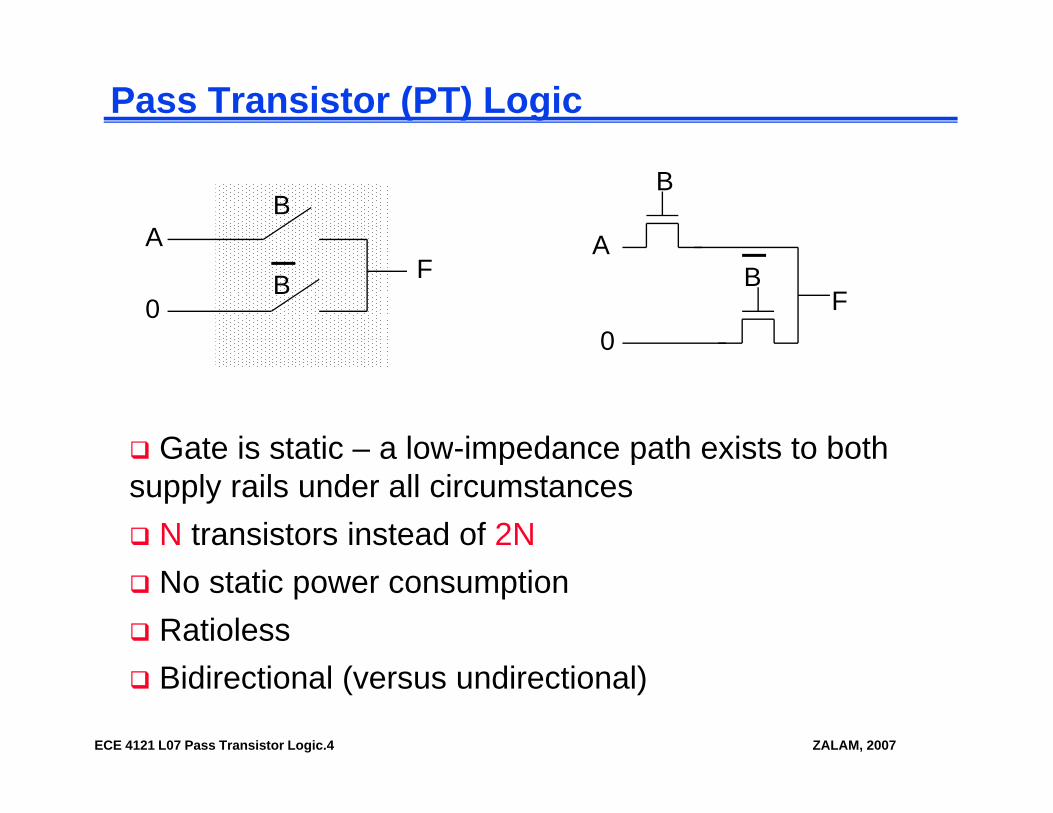
Pass Transistor (PT) Logic
AB
A
B
FB0
A
0
BF
Gate is static – a low-impedance path exists to bothGate is static a low impedance path exists to both supply rails under all circumstances
N transistors instead of 2NNo static power consumptionRatioless
ECE 4121 L07 Pass Transistor Logic.4 ZALAM, 2007
Bidirectional (versus undirectional)
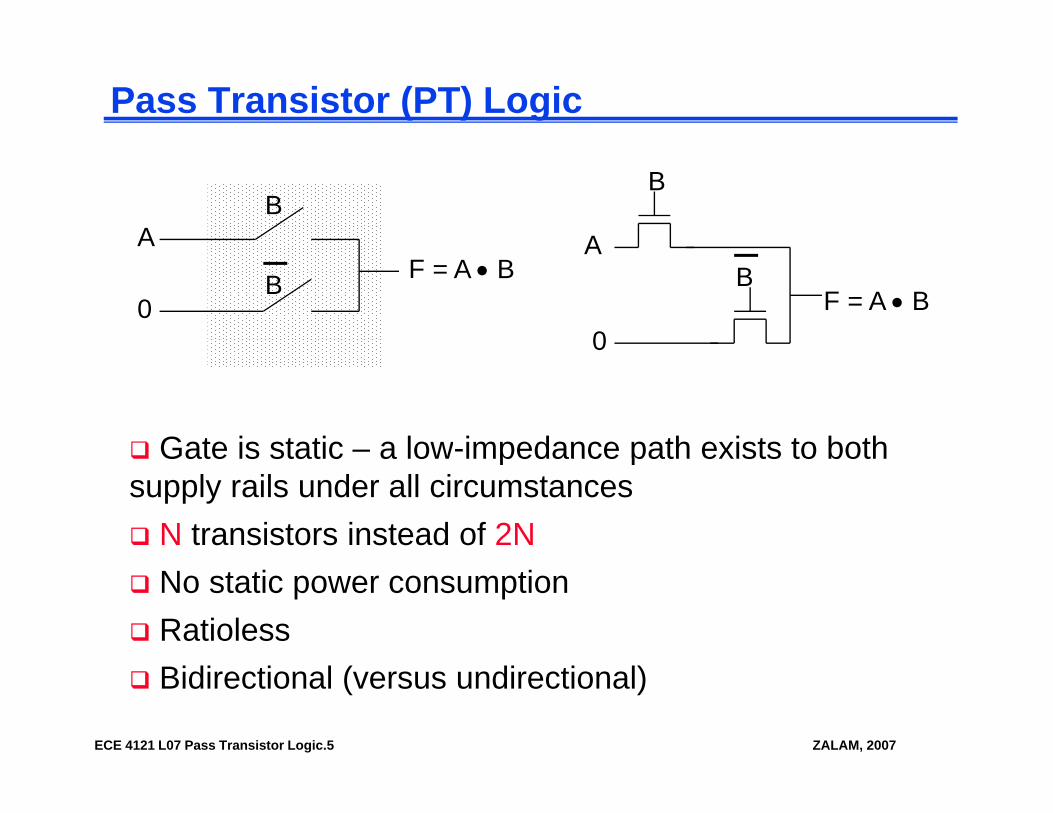
Pass Transistor (PT) Logic
AB
A
B
FB0
A
0
B= A • BF = A • B
Gate is static – a low-impedance path exists to bothGate is static a low impedance path exists to both supply rails under all circumstances
N transistors instead of 2NNo static power consumptionRatioless
ECE 4121 L07 Pass Transistor Logic.5 ZALAM, 2007
Bidirectional (versus undirectional)

VTC of PT AND Gate
B1 5/0 25
0.5/0.25
1.5/0.25 2
B=VDD, A=0→VDD
V out, V
AB F= A•B
0.5/0.251
A=VDD, B=0→VDDA=B=0→VDD
V0 0.5/0.25
00 1 2
DD
Pure PT logic is not regenerative - the signal gradually degrades after passing through a number
ECE 4121 L07 Pass Transistor Logic.6 ZALAM, 2007
of PTs (can fix with static CMOS inverter insertion)

Differential PT Logic (CPL)A
B
AB
PT Network FF
AAB
Inverse PT Network FF
BNetwork
B B BB BB
A
B F=AB
B B
A
B F=A+BA
A F=A⊕B
F=ABA
B F AB
B
A
B
BF=A+B
A
F=A⊕BA
A
ECE 4121 L07 Pass Transistor Logic.7 ZALAM, 2007
BAND/NAND OR/NOR XOR/XNOR
A

CPL Properties
Differential so complementary data inputs and outputs are always available (so don’t need extra inverters)
Still static, since the output defining nodes are always tied to VDD or GND through a low resistance path
D i i d l ll t th t l lDesign is modular; all gates use the same topology, only the inputs are permuted.
Simple XOR makes it attractive for structures like addersSimple XOR makes it attractive for structures like adders
Fast (assuming number of transistors in series is small)
Additional routing overhead for complementary signals
Still have static power dissipation problems
ECE 4121 L07 Pass Transistor Logic.8 ZALAM, 2007

CPL Full Adder
A
BB CinCin
!SumA
A
!Sum
SumSum
BB Cin Cin
!CoutA
B Cin
CoutA
B Cin
ECE 4121 L07 Pass Transistor Logic.9 ZALAM, 2007

CPL Full Adder
A
BB CinCin
!SumA
A
!Sum
SumSum
BB Cin Cin
!CoutA
B Cin
CoutA
B Cin
ECE 4121 L07 Pass Transistor Logic.10 ZALAM, 2007

NMOS Only PT Driving an Inverter
In = VDDVx = V V
M2VGSA = VDDVDD-VTn
M1
2
BSD
VGS
Vx does not pull up to VDD, but VDD – VTnVx does not pull up to VDD, but VDD VTn
Threshold voltage drop causes static power consumption (M may be weakly conducting forming aconsumption (M2 may be weakly conducting forming a path from VDD to GND)
Notice VTn increases of pass transistor due to body
ECE 4121 L07 Pass Transistor Logic.11 ZALAM, 2007
Notice VTn increases of pass transistor due to body effect (VSB)

Voltage Swing of PT Driving an Inverter
In = 0 → VDD
3In
VDDx Out
0.5/0.25
1.5/0.25
1
2
ltage
, V
x = 1.8VD
S
0.5/0.25
0
1
Vo
OutB
Body effect – large VSB at x - when pulling high (B is i d GND d S h d l V )
0 0.5 1 1.5 2Time, ns
tied to GND and S charged up close to VDD)
So the voltage drop is even worse
ECE 4121 L07 Pass Transistor Logic.12 ZALAM, 2007
Vx = VDD - (VTn0 + γ(√(|2φf| + Vx) - √|2φf|))

Cascaded NMOS Only PTs
B = VDD
xM
B = VDD
OutyM
C = VDD
A VG
Out
M1
yM2
xM1 OutyM2A = VDD
C = V
A = VDDx = VDD - VTn1G
S
OutM2
Swing on y = VDD - VTn1 - VTn2 Swing on y = VDD - VTn1
C = VDD S
g y DD Tn1 Tn2 g y DD Tn1
Pass transistor gates should never be cascaded as onPass transistor gates should never be cascaded as on the leftLogic on the right suffers from static power dissipation
ECE 4121 L07 Pass Transistor Logic.13 ZALAM, 2007
and reduced noise margins

Solution 1: Level Restorer
Level Restorer
Mon
M2
A=0 Mn
Mr
x
B
Out =1
off
= 0A=1 Out=0
1M1
A 0 n Out 11
Full swing on x (due to Level Restorer) so no static power consumption by inverter
F t ti M t b i d tl ( ti d)
No static backward current path through Level Restorer and PT since Restorer is only active when A is high
ECE 4121 L07 Pass Transistor Logic.14 ZALAM, 2007
For correct operation Mr must be sized correctly (ratioed)

Transient Level Restorer Circuit Response3 W/L2=1.50/0.253
W/Ln=0.50/0.252
W/L1=0.50/0.25
2
V
W/Lr=1.75/0.25
node x never goes below VMof inverter so output never switches
1
Volta
ge, V
W/Lr=1.50/0.25
0
W/Lr=1.25/0.25W/Lr=1.0/0.25
0 100 200 300 400 500Time, ps
Restorer has speed and power impacts: increases the
ECE 4121 L07 Pass Transistor Logic.15 ZALAM, 2007
p p pcapacitance at x, slowing down the gate; increases tr (but decreases tf)

Solution 2: Multiple VT TransistorsTechnology solution: Use (near) zero VT devices for theTechnology solution: Use (near) zero VT devices for the NMOS PTs to eliminate most of the threshold drop (body effect still in force preventing full swing to VDD)
In2 = 0V A= 2.5V
low VT transistors
Out
on
In1 = 2.5V B = 0V
off but leaking
Impacts static power consumption due to subthreshold
sneak path
ECE 4121 L07 Pass Transistor Logic.16 ZALAM, 2007
Impacts static power consumption due to subthreshold currents flowing through the PTs (even if VGS is below VT)

Solution 3: Transmission Gates (TGs)Most widely used C
A B
CMost widely used solution
A B
C
C
C
C = GND C = GND
BA = VDD BA = GND
Full swing bidirectional switch controlled by the gate
C = VDD C = VDD
ECE 4121 L07 Pass Transistor Logic.17 ZALAM, 2007
Full swing bidirectional switch controlled by the gate signal C, A = B if C = 1

Solution 3: Transmission Gates (TGs)Most widely used
C
A B
CMost widely used solution
A B
C
C
C
C = GND C = GND
BA = VDD BA = GND
Full swing bidirectional switch controlled by the gate
C = VDD C = VDD
ECE 4121 L07 Pass Transistor Logic.18 ZALAM, 2007
Full swing bidirectional switch controlled by the gate signal C, A = B if C = 1

Resistance of TG
300V
W/Lp=0.50/0.25
20
25
Ω
Rp
2.5V VoutR
Rn
10
15
sist
ance
, kΩ
Rn
2.5V
Rp
R W/L 0 50/0 25
0
5
0 1 2
Re Req W/Ln=0.50/0.25
0 1 2
ECE 4121 L07 Pass Transistor Logic.19 ZALAM, 2007

TG Multiplexer
VDD
S S
SF
In2
S
In1
F
S
1
GND
In1 In2S S
F = !(In1 • S + In2 • S)
ECE 4121 L07 Pass Transistor Logic.20 ZALAM, 2007
1 2

Transmission Gate XOR
A A ⊕ B
BB
ECE 4121 L07 Pass Transistor Logic.21 ZALAM, 2007

Transmission Gate XOR
ff
weak 0 if !A
A !BA A ⊕ B
off
off B • !A
on
on
A • !B
B0 weak 1 if A
B1
an inverter
ECE 4121 L07 Pass Transistor Logic.22 ZALAM, 2007

TG Full Adder
Cin
B
SumA Sum
Cout
ECE 4121 L07 Pass Transistor Logic.23 ZALAM, 2007

Differential TG Logic (DPL)
A
B A B A
A
B A B A
A
A
B F=A⊕BF=AB
A
B
GND
B
A
B
GND
F=A⊕B
A
BF=ABA
VDD
AND/NAND XOR/XNOR
A
B
VDD
B
ECE 4121 L07 Pass Transistor Logic.24 ZALAM, 2007

Next Time: The MOS Transistor
MOS transistor dynamic behavior (R and C))
Wire capacitance
ECE 4121 L07 Pass Transistor Logic.25 ZALAM, 2007