Embed Size (px)
Citation preview
Minimizing Spurious Switching Activities with TransistorSizing*
ARTUR WROBLEWSKIa,†, CHRISTIAN V. SCHIMPFLEb, OTTO SCHUMACHERc and JOSEF A. NOSSEKa
aMunich University of Technology, Arcisstr. 21, 80333 Munchen, Germany; bTexas Instruments Deutschland, 85350 Freising, Germany; cInfineonTechnologies AG, P.O. Box 800949, 81609 Munchen, Germany
(Received 27 April 2001; Revised 11 June 2001)
In combinatorial blocks of static CMOS circuits transistor sizing can be applied for delay balancing asto guarantee synchronously arriving signal slopes at the input of logic gates, thereby avoiding glitches.Since the delay of logic gates depends directly on transistor sizes, their variation allows equalizingdifferent path delays without influencing the total delay of the circuit. Unfortunately, not only the delay,but also power consumption circuits depend on the transistor sizes. To achieve optimal results,transistor lengths have to be increased, which results in both increased gate capacitances and area.Splitting the long transistors counteracts this negative influence.
Keywords: Glitches; Transistor sizing; VLSI; Low-power; CMOS
INTRODUCTION
Optimal sizing of MOS-transistors is a widely investigated
method for the design of CMOS-circuits with restricted
area, propagation delay or power consumption. A large
number of the previously published approaches aim at
area and power optimization under given delay constraints
[1–3]. Optimal area utilization is still important, but since
the substantial progress in development of deep submicron
techniques, power dissipation has become the main
limiting factor. The power consumption models often
include only the power consumed for charging transistor
gate- and drain/source-capacitances. The power models in
Ref. [1] include also the dissipation caused by short-
circuit currents that occur during transition when both
P- and N-transistors of a CMOS-stage are conducting.
Delay balancing for reducing the glitching activities in
combinational Wallace-trees and array multipliers has
been introduced in Ref. [4].
Unlike for most approaches that focus on maximizing
the speed of a circuit by variation of transistor widths, the
method presented here also allows the transistor lengths
to be variable. Reducing speed for delay balancing is only
allowed for parts of the circuit that are not in the critical
path. In Ref. [5] a method is presented, where all
transistor widths outside the critical path are reduced in
order to reduce the total capacitance of the circuit.
However, delay balancing may not be possible if only the
widths are variable because the limit here is the minimum
feature size. Further speed reduction can then be achieved
by increasing the transistor length. In order to keep track
of the conflicting design objectives like increasing
transistor sizes for delay balancing, and at the same
time reducing the total power consumption caused by
charging capacitances, the method is formulated as a
multiobjective optimization problem. Furthermore, by
introduction of changes to the topology of the circuit
where possible, the reduction of gate capacitances can be
achieved. This makes further decrease in power
dissipation possible.
In the following we consider circuits in which
increasing transistor lengths is necessary. Decreasing of
W to make the gate slower, which is the usual approach,
results in smaller area and less power consumption. On the
contrary increasing L provides slower gates, but influences
both, the area and power dissipation, negatively. Thus,
increasing L represents the worst case approach to
transistor sizing. Therefore, the power savings presented
here reflect only the benefits of a delay balanced circuit
due to reduced glitch activity. Of course GliMATS, a
program that has been implemented for automated circuit
optimization, is not limited by this artificial constraint.
ISSN 1065-514X print/ISSN 1563-5171 online q 2002 Taylor & Francis Ltd
DOI: 10.1080/1065514021000012156
*Portions reprinted, with permission, from “Automated Transistor Sizing Algorithm For Minimizing Spurious Switching Activities in CMOSCircuits” ISCAS’00 q2000 IEEE and “Minimizing Gate Capacitances with Transistor Sizing” ISCAS’01 q2001 IEEE.
†Corresponding author. E-mail: [email protected]
VLSI Design, 2002 Vol. 15 (2), pp. 537–545
DELAY AND POWER MODELS
The delay and power models used for the transistor sizing
method presented here are defined at gate level. Although
transistor level models may offer more degrees of freedom
and allow individual sizing of each single transistor, it
turns out to be more desirable to have a low dimensional
optimization problem in order to be able to optimize larger
circuits within acceptable computation time. When
modeling a circuit at gate level (macromodeling ), the
relatively large number of local parameters that describe
every single transistor is reduced to a set of scale factors
for each gate. In the considered case the number of
variables is reduced to one specific W and one specific L
for each gate. If W and/or L are varied, all transistor widths
and/or lengths within the gate are scaled by the same
factor simultaneously.
Delay Model
The macromodel delay has to be described for each type of
logic gate separately. In the following, the delay model is
derived exemplarily for a 2-input CMOS AND gate. The
generalization to any other logic gate type is straightfor-
ward. The delay of a gate at position m can be split up into
two parts [3,6]: The step response delay ts;m; which is
independent from the input signal form, and tin;m; which is
the contribution caused by the finite input signal rise and
fall times. The total delay tm is then approximated by
tm ¼ tin;m þ ts;m: ð1Þ
The optimization method aims at the minimization of
glitches, which necessitates equalizing all path delays.
However, the step response delay ts;m depends on the input
transition. For example, the step response delay of a
2-input AND gate in 0.25mm technology with a certain
load is 0.4 ns for the input transition 11 ! 00 and 0.75 ns
for 00 ! 11: Therefore, the different paths can exactly be
balanced for one special transition only. Experiments have
shown that the worst case delay is a good choice and is
easy to formulate in the model. Furthermore, numerous
simulations based on this model show, that although the
paths cannot be exactly balanced for all transitions,
glitching could be eliminated to a large amount. The step
response delay ts;m is described with Elmore’s delay
model. It is assumed that there is a fixed ratio r between
N- and PMOS transistor sizes
Wm
Lm
� �p
¼ rWm
Lm
� �n
!ð2Þ
to achieve Rn;m ¼ Rp;m ¼ Rm for the channel resistances of
N- and PMOS transistors. The drain/source and gate
capacitances can then be written as
Cd=sn;m ¼ Cd=s;m; Cd=sp;m ¼ rCd=s;m ð3Þ
and
Cgn;m ¼ Cg;m; Cgp;m ¼ rCg;m: ð4Þ
All components can be formulated as functions of the
channel length and width:
Rm ¼ rLm
Wm
ð5Þ
Cd=s;m ¼ cd=sWm ð6Þ
and
Cg;m ¼ cgWmLm ð7Þ
where r; cd=s and cg denote process dependent constants.
The load capacitance depends on the transistor sizes at
position m þ 1 and the number of input transistor gates
kmþ1 at position m þ 1, in such a way that
CL;m ¼ kmþ1cgWmþ1Lmþ1: ð8Þ
For the 2-input AND gate follows
ts;m ¼ rcd=sð5 þ 3rÞLm þ 2rcgð1 þ rÞL2m
þ rcgð1 þ rÞLm
Wm
Wmþ1Lmþ1
ð9Þ
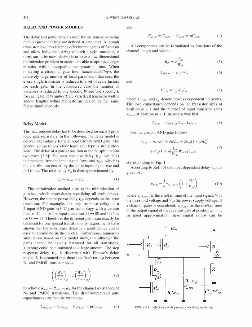
corresponding to Fig. 1.
According to Ref. [3] the input dependent delay tm;in is
given by:
tm;in ¼1
6tr=f ;m21 1 þ
2Vt
Vdd
� �ð10Þ
where tr=f ;m21 is the rise/fall time of the input signal, Vt is
the threshold voltage and Vdd the power supply voltage. If
a chain of gates is considered, tr=f ;m21 is the rise/fall time
of the output signal of the previous gate at position m 2 1.
In good approximation these signal ramps can be
FIGURE 1 AND gate with parasitics for delay modeling.
A. WROBLEWSKI et al.538
considered to be quasi-linear, such that tr=f ;m21 in Eq. (10)
can be replaced by its linear approximation teff ;m21 which
is given by:
teff ;m21 ¼8
3 ln 3ts;m21 1 2 0:27
Vt
Vdd
� �: ð11Þ
For details see Ref. [3]. The input dependent delay can
then be written as:
tm;in ¼4
9 ln 31 þ 1:73
Vt
Vdd
2 0:54Vt
Vdd
� �2 !
·ts;m21
¼ K·ts;m21
ð12Þ
where all technology dependent parameters are merged in
the constant K. With Eqs. (1), (9) and (12) the total gate
delay is given by:
tm ¼ K·ðrcd=sð5 þ 3rÞLm21 þ 2rcgð1 þ rÞL2m21
þ rcgð1 þ rÞLm21
Wm21
WmLmÞ þ rcd=sð5
þ 3rÞLm þ 2rcgð1 þ rÞL2m þ rcgð1 þ rÞ
�Lm
Wm
Wmþ1Lmþ1
¼ k1Lm21 þ k2L2m21 þ k3
Lm21
Wm21
LmWm þ k4Lm
þ k5L2m þ k6
Lm
Wm
Lmþ1Wmþ1: ð13Þ
All technology dependent parameters are merged in
constants k1...6: The total delay of a path number n is
the sum over all gate delays in this path:
tn ¼Xn
m¼1
tm; ð14Þ
where n is the number of gates in the path.
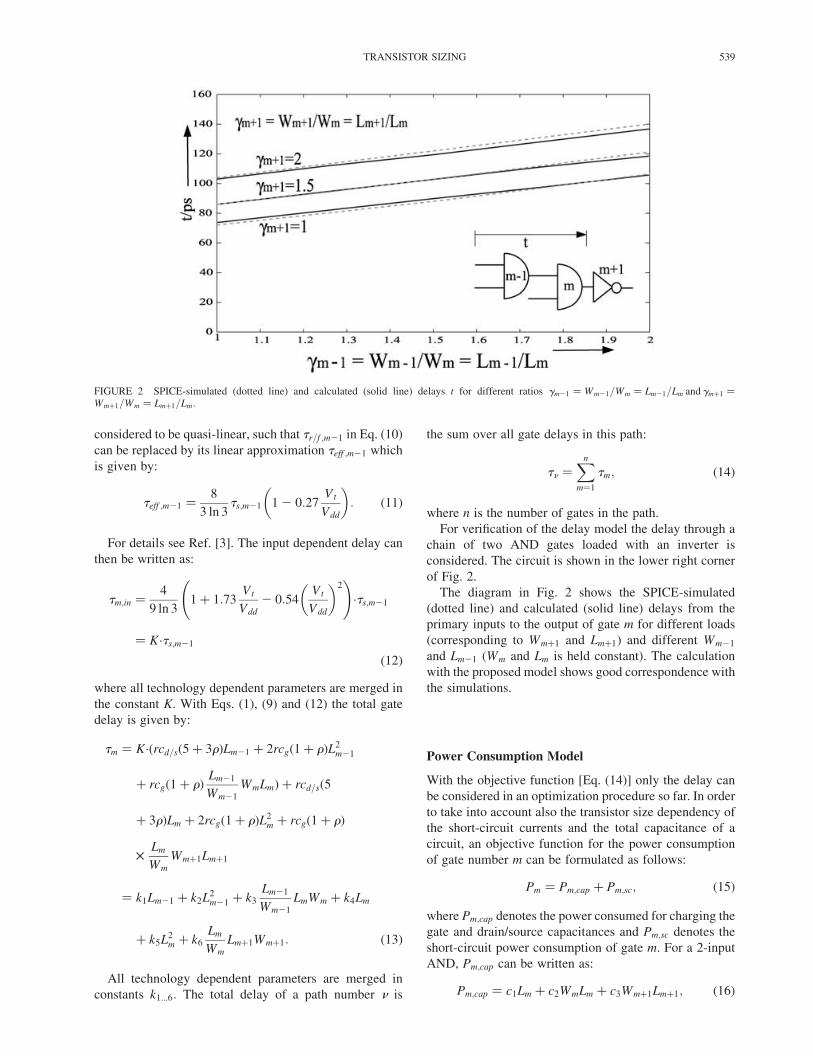
For verification of the delay model the delay through a
chain of two AND gates loaded with an inverter is
considered. The circuit is shown in the lower right corner
of Fig. 2.
The diagram in Fig. 2 shows the SPICE-simulated
(dotted line) and calculated (solid line) delays from the
primary inputs to the output of gate m for different loads
(corresponding to Wmþ1 and Lmþ1) and different Wm21
and Lm21 (Wm and Lm is held constant). The calculation
with the proposed model shows good correspondence with
the simulations.
Power Consumption Model
With the objective function [Eq. (14)] only the delay can
be considered in an optimization procedure so far. In order
to take into account also the transistor size dependency of
the short-circuit currents and the total capacitance of a
circuit, an objective function for the power consumption
of gate number m can be formulated as follows:
Pm ¼ Pm;cap þ Pm;sc; ð15Þ
where Pm;cap denotes the power consumed for charging the
gate and drain/source capacitances and Pm;sc denotes the
short-circuit power consumption of gate m. For a 2-input
AND, Pm;cap can be written as:
Pm;cap ¼ c1Lm þ c2WmLm þ c3Wmþ1Lmþ1; ð16Þ
FIGURE 2 SPICE-simulated (dotted line) and calculated (solid line) delays t for different ratios gm21 ¼ Wm21=Wm ¼ Lm21=Lm and gmþ1 ¼Wmþ1=Wm ¼ Lmþ1=Lm:
TRANSISTOR SIZING 539
where
c1 ¼ f V2ddða1cd=sð1 þ 2rÞ þ 2a2cd=sÞ; ð17Þ
c2 ¼ f V2dda1cgð1 þ rÞ ð18Þ
and
c3 ¼ a3f V2ddðcd=sð1 þ rÞ þ cgkmþ1ð1 þ rÞÞ: ð19Þ
Factors a1;a2; and a3, denote the switching activities at
nodes 1, 2, and 3, respectively (see the numbers in circles
in Fig. 1), which are considered as constants over W and L.
The short-circuit power dissipation of a CMOS inverter
according to Ref. [7] is given by:
Pm;sc ¼ teff ;m21
bm
12f ðVdd 2 2VtÞ
3: ð20Þ
bm is the transistor gain factor ðbm , Wm=LmÞ and teff ;m21
is given in Eq. (11). For a 0.25mm technology and Vdd ¼
2:5 V
Pm;sc < 0:00045fWm
Lm
ts;m21: ð21Þ
It can be shown experimentally, that neglecting the
contribution of Pm;sc has no negative influence on the
results of the path balancing method even for complex
gates. Therefore, it is reasonable to set Pm ¼ Pm;cap: The
total transistor size dependent power consumption in path
number n can be formulated as:
Pn ¼Xn
m¼1
Pm; ð22Þ
for a path with n gates.
MULTIOBJECTIVE OPTIMIZATION
In order to find a power optimal solution for W and L the
designer is confronted with two conflicting design criteria:
path balancing by transistor sizing, achieved by enlarging
transistors, and low power consumption for charging
capacitances which requires small transistors at the same
time. This problem usually can be solved with a non-linear
programming method. A common approach to find a
solution is to keep one of the design criteria within upper
and lower bounds and find an optimal solution for the
other one under these restrictions. The problem is to
determine the upper and lower bounds if they are not
previously known. Awkwardly chosen bounds may result
in an unsolvable optimization problem. Therefore, not
every single criterion is optimized while restricting all the
others, but the weighted sum of all the design criteria [3].
In order to equalize all the path delays with respect to the
critical path, every path requires individual optimization.
Let tcrit denote the critical path delay of the circuit.
For every path n a solution of
W ;Lminjtn 2 tcritj ð23Þ
must be calculated to achieve path balancing. The path
delay tn is defined in Eq. (14). The power consumption
according to Eq. (22) is minimized by
W ;Lmin ðPn ¼
Xn
m¼1
PmÞ: ð24Þ
Equations (23) and (24) describe convex optimization
problems in W and L. The multiobjective optimization
problem is given by:
W;Lmin ðSn ¼ w · ðtn 2 tcritÞ
2 þ ð1 2 wÞ · PnÞ: ð25Þ
The weight factor w varies between 0 and 1, w [ ½0; 1�:Results of the optimization are highly independent of the
choice of w. Only values extremely close to 0 or 1
influence the result. In order to obtain a cost function,
which is differentiable everywhere, jtn 2 tcritj is replaced
by its square. The upper and lower bounds of the transistor
sizes are determined by the minimum feature size of the
used technology and the user defined limits for the
maximum available area for a single transistor.
Assigning a value to w allows a solution to be chosen
depending on which of the design objectives is more
desired: low power consumption caused by the total
capacitive load or balanced path delays. However,
experiments have shown that for many circuits the best
low power solution is obtained if jt2 tcritj ¼ 0; i.e. for
optimally balanced paths. This is usually given when w ¼
0:5. . .1:
MINIMIZING GATE CAPACITANCES
As mentioned before, the case considered in this paper is
the one, when transistors are being made longer. This
leads to larger channel resistance of the transistor and
increases its gate capacitance. In the following we present
two alternative ways of reducing this negative influence.
“Twin-transistors”
So far the channel resistance as well as the gate
capacitance
Rch , rch
L
W; CG , cGLW ð26Þ
are proportional to the channel length. On the other hand
the delay is proportional to both, the channel resistance
and gate capacitance. To increase the channel resistance
without increasing the gate capacitance one has to be able
to change them independently from each other. This is
possible if the capacitance and the resistance are no longer
A. WROBLEWSKI et al.540
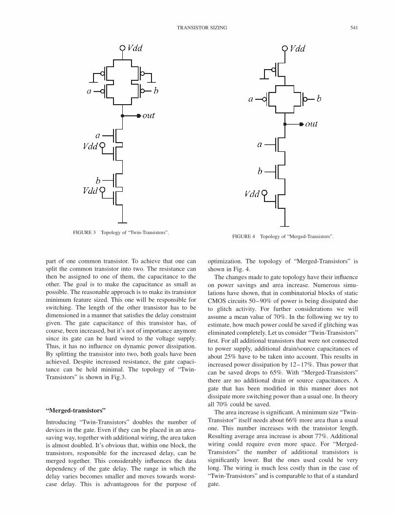
part of one common transistor. To achieve that one can
split the common transistor into two. The resistance can
then be assigned to one of them, the capacitance to the
other. The goal is to make the capacitance as small as
possible. The reasonable approach is to make its transistor
minimum feature sized. This one will be responsible for
switching. The length of the other transistor has to be
dimensioned in a manner that satisfies the delay constraint
given. The gate capacitance of this transistor has, of
course, been increased, but it’s not of importance anymore
since its gate can be hard wired to the voltage supply.
Thus, it has no influence on dynamic power dissipation.
By splitting the transistor into two, both goals have been
achieved. Despite increased resistance, the gate capaci-
tance can be held minimal. The topology of “Twin-
Transistors” is shown in Fig.3.
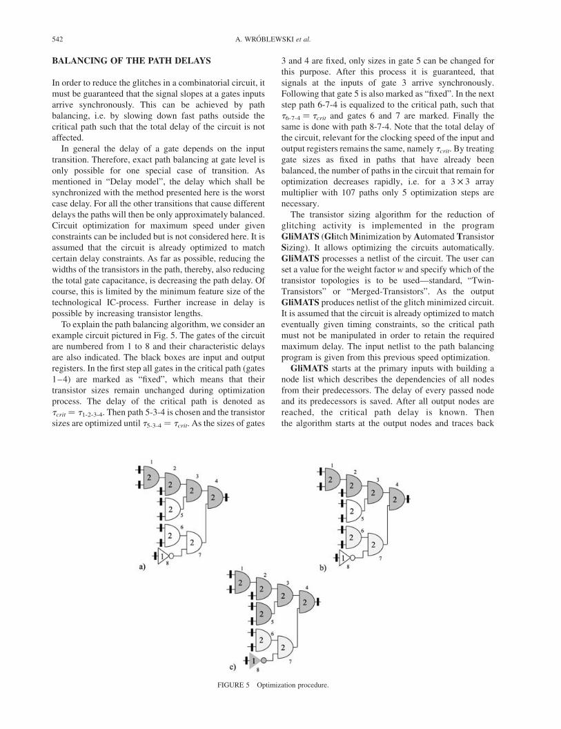
“Merged-transistors”
Introducing “Twin-Transistors” doubles the number of
devices in the gate. Even if they can be placed in an area-
saving way, together with additional wiring, the area taken
is almost doubled. It’s obvious that, within one block, the
transistors, responsible for the increased delay, can be
merged together. This considerably influences the data
dependency of the gate delay. The range in which the
delay varies becomes smaller and moves towards worst-
case delay. This is advantageous for the purpose of
optimization. The topology of “Merged-Transistors” is
shown in Fig. 4.
The changes made to gate topology have their influence
on power savings and area increase. Numerous simu-
lations have shown, that in combinatorial blocks of static
CMOS circuits 50–90% of power is being dissipated due
to glitch activity. For further considerations we will
assume a mean value of 70%. In the following we try to
estimate, how much power could be saved if glitching was
eliminated completely. Let us consider “Twin-Transistors”
first. For all additional transistors that were not connected
to power supply, additional drain/source capacitances of
about 25% have to be taken into account. This results in
increased power dissipation by 12–17%. Thus power that
can be saved drops to 65%. With “Merged-Transistors”
there are no additional drain or source capacitances. A
gate that has been modified in this manner does not
dissipate more switching power than a usual one. In theory
all 70% could be saved.
The area increase is significant. A minimum size “Twin-
Transistor” itself needs about 66% more area than a usual
one. This number increases with the transistor length.
Resulting average area increase is about 77%. Additional
wiring could require even more space. For “Merged-
Transistors” the number of additional transistors is
significantly lower. But the ones used could be very
long. The wiring is much less costly than in the case of
“Twin-Transistors” and is comparable to that of a standard
gate.
FIGURE 3 Topology of “Twin-Transistors”.FIGURE 4 Topology of “Merged-Transistors”.
TRANSISTOR SIZING 541
BALANCING OF THE PATH DELAYS
In order to reduce the glitches in a combinatorial circuit, it
must be guaranteed that the signal slopes at a gates inputs
arrive synchronously. This can be achieved by path
balancing, i.e. by slowing down fast paths outside the
critical path such that the total delay of the circuit is not
affected.
In general the delay of a gate depends on the input
transition. Therefore, exact path balancing at gate level is
only possible for one special case of transition. As
mentioned in “Delay model”, the delay which shall be
synchronized with the method presented here is the worst
case delay. For all the other transitions that cause different
delays the paths will then be only approximately balanced.
Circuit optimization for maximum speed under given
constraints can be included but is not considered here. It is
assumed that the circuit is already optimized to match
certain delay constraints. As far as possible, reducing the
widths of the transistors in the path, thereby, also reducing
the total gate capacitance, is decreasing the path delay. Of
course, this is limited by the minimum feature size of the
technological IC-process. Further increase in delay is
possible by increasing transistor lengths.
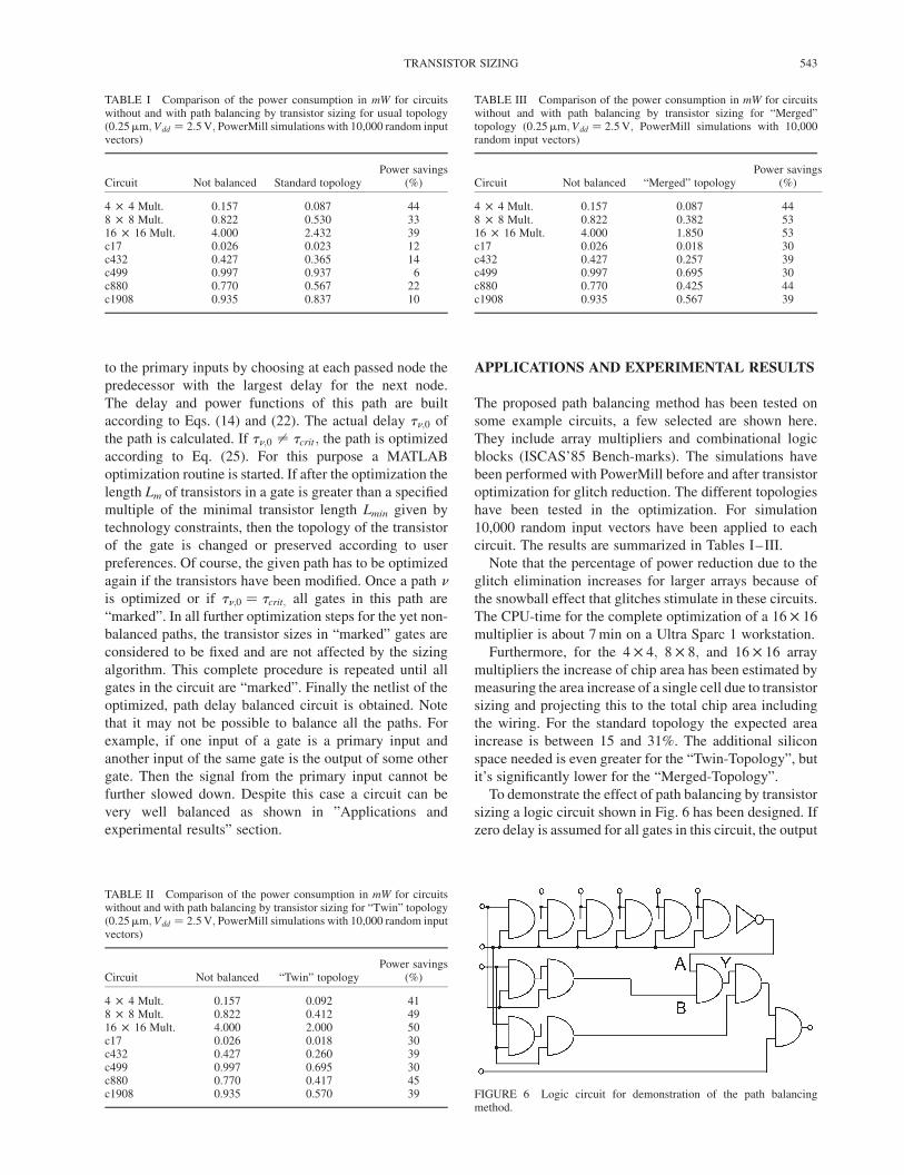
To explain the path balancing algorithm, we consider an
example circuit pictured in Fig. 5. The gates of the circuit
are numbered from 1 to 8 and their characteristic delays
are also indicated. The black boxes are input and output
registers. In the first step all gates in the critical path (gates
1–4) are marked as “fixed”, which means that their
transistor sizes remain unchanged during optimization
process. The delay of the critical path is denoted as
tcrit ¼ t1-2-3-4. Then path 5-3-4 is chosen and the transistor
sizes are optimized until t5-3-4 ¼ tcrit. As the sizes of gates
3 and 4 are fixed, only sizes in gate 5 can be changed for
this purpose. After this process it is guaranteed, that
signals at the inputs of gate 3 arrive synchronously.
Following that gate 5 is also marked as “fixed”. In the next
step path 6-7-4 is equalized to the critical path, such that
t6-7-4 ¼ tcrit and gates 6 and 7 are marked. Finally the
same is done with path 8-7-4. Note that the total delay of
the circuit, relevant for the clocking speed of the input and
output registers remains the same, namely tcrit. By treating
gate sizes as fixed in paths that have already been
balanced, the number of paths in the circuit that remain for
optimization decreases rapidly, i.e. for a 3 £ 3 array
multiplier with 107 paths only 5 optimization steps are
necessary.
The transistor sizing algorithm for the reduction of
glitching activity is implemented in the program
GliMATS (Glitch Minimization by Automated Transistor
Sizing). It allows optimizing the circuits automatically.
GliMATS processes a netlist of the circuit. The user can
set a value for the weight factor w and specify which of the
transistor topologies is to be used—standard, “Twin-
Transistors” or “Merged-Transistors”. As the output
GliMATS produces netlist of the glitch minimized circuit.
It is assumed that the circuit is already optimized to match
eventually given timing constraints, so the critical path
must not be manipulated in order to retain the required
maximum delay. The input netlist to the path balancing
program is given from this previous speed optimization.
GliMATS starts at the primary inputs with building a
node list which describes the dependencies of all nodes
from their predecessors. The delay of every passed node
and its predecessors is saved. After all output nodes are
reached, the critical path delay is known. Then
the algorithm starts at the output nodes and traces back
FIGURE 5 Optimization procedure.
A. WROBLEWSKI et al.542
to the primary inputs by choosing at each passed node the
predecessor with the largest delay for the next node.
The delay and power functions of this path are built
according to Eqs. (14) and (22). The actual delay tn;0 of
the path is calculated. If tn;0 – tcrit; the path is optimized
according to Eq. (25). For this purpose a MATLAB
optimization routine is started. If after the optimization the
length Lm of transistors in a gate is greater than a specified
multiple of the minimal transistor length Lmin given by
technology constraints, then the topology of the transistor
of the gate is changed or preserved according to user
preferences. Of course, the given path has to be optimized
again if the transistors have been modified. Once a path n
is optimized or if tn;0 ¼ tcrit; all gates in this path are
“marked”. In all further optimization steps for the yet non-
balanced paths, the transistor sizes in “marked” gates are
considered to be fixed and are not affected by the sizing
algorithm. This complete procedure is repeated until all
gates in the circuit are “marked”. Finally the netlist of the
optimized, path delay balanced circuit is obtained. Note
that it may not be possible to balance all the paths. For
example, if one input of a gate is a primary input and
another input of the same gate is the output of some other
gate. Then the signal from the primary input cannot be
further slowed down. Despite this case a circuit can be
very well balanced as shown in ”Applications and
experimental results” section.
APPLICATIONS AND EXPERIMENTAL RESULTS
The proposed path balancing method has been tested on
some example circuits, a few selected are shown here.
They include array multipliers and combinational logic
blocks (ISCAS’85 Bench-marks). The simulations have
been performed with PowerMill before and after transistor
optimization for glitch reduction. The different topologies
have been tested in the optimization. For simulation
10,000 random input vectors have been applied to each
circuit. The results are summarized in Tables I–III.
Note that the percentage of power reduction due to the
glitch elimination increases for larger arrays because of
the snowball effect that glitches stimulate in these circuits.
The CPU-time for the complete optimization of a 16 £ 16
multiplier is about 7 min on a Ultra Sparc 1 workstation.
Furthermore, for the 4 £ 4; 8 £ 8; and 16 £ 16 array
multipliers the increase of chip area has been estimated by
measuring the area increase of a single cell due to transistor
sizing and projecting this to the total chip area including
the wiring. For the standard topology the expected area
increase is between 15 and 31%. The additional silicon
space needed is even greater for the “Twin-Topology”, but
it’s significantly lower for the “Merged-Topology”.
To demonstrate the effect of path balancing by transistor
sizing a logic circuit shown in Fig. 6 has been designed. If
zero delay is assumed for all gates in this circuit, the output
TABLE I Comparison of the power consumption in mW for circuitswithout and with path balancing by transistor sizing for usual topology(0:25mm;Vdd ¼ 2:5 V; PowerMill simulations with 10,000 random inputvectors)
Circuit Not balanced Standard topologyPower savings
(%)
4 £ 4 Mult. 0.157 0.087 448 £ 8 Mult. 0.822 0.530 3316 £ 16 Mult. 4.000 2.432 39c17 0.026 0.023 12c432 0.427 0.365 14c499 0.997 0.937 6c880 0.770 0.567 22c1908 0.935 0.837 10
TABLE III Comparison of the power consumption in mW for circuitswithout and with path balancing by transistor sizing for “Merged”topology (0:25mm;Vdd ¼ 2:5 V; PowerMill simulations with 10,000random input vectors)
Circuit Not balanced “Merged” topologyPower savings
(%)
4 £ 4 Mult. 0.157 0.087 448 £ 8 Mult. 0.822 0.382 5316 £ 16 Mult. 4.000 1.850 53c17 0.026 0.018 30c432 0.427 0.257 39c499 0.997 0.695 30c880 0.770 0.425 44c1908 0.935 0.567 39
FIGURE 6 Logic circuit for demonstration of the path balancingmethod.
TABLE II Comparison of the power consumption in mW for circuitswithout and with path balancing by transistor sizing for “Twin” topology(0:25mm;Vdd ¼ 2:5 V; PowerMill simulations with 10,000 random inputvectors)
Circuit Not balanced “Twin” topologyPower savings
(%)
4 £ 4 Mult. 0.157 0.092 418 £ 8 Mult. 0.822 0.412 4916 £ 16 Mult. 4.000 2.000 50c17 0.026 0.018 30c432 0.427 0.260 39c499 0.997 0.695 30c880 0.770 0.417 45c1908 0.935 0.570 39
TRANSISTOR SIZING 543
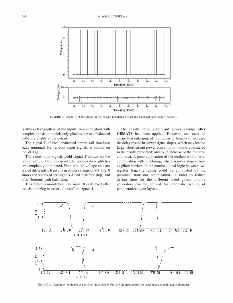
is always 0 regardless of the inputs. In a simulation with
complex transistor models only glitches due to unbalanced
paths are visible at the output.
The signal Y of the unbalanced circuit (all transistor
sizes minimal) for random input signals is shown on
top of Fig. 7.
The same input signals yield signal Y shown on the
bottom of Fig. 7 for the circuit after optimization: glitches
are completely eliminated. Note that the voltage axis are
scaled differently. It results in power savings of 8%. Fig. 8
shows the slopes of the signals A and B before (top) and
after (bottom) path balancing.
This figure demonstrates how signal B is delayed after
transistor sizing in order to “wait” on signal A.
The results show significant power savings after
GliMATS has been applied. However, one must be
aware that enlarging of the transistor lengths to increase
the delay results in slower signal slopes, which may lead to
larger short circuit power consumption (this is considered
in the results presented) and to an increase of the required
chip area. A good application of the method would be in
combination with pipelining, where register stages work
as glitch barriers. In the combinational logic between two
register stages glitching could be eliminated by the
presented transistor optimization. In order to reduce
design time for the different sized gates, module
generators can be applied for automatic scaling of
parameterized gate layouts.
FIGURE 7 Signal Y of the circuit in Fig. 6 with unbalanced (top) and balanced path delays (bottom).
FIGURE 8 Example for signals A and B of the circuit in Fig. 6 with unbalanced (top) and balanced path delays (bottom).
A. WROBLEWSKI et al.544
CONCLUSION
In this work a method for transistor size optimization to
achieve equal path delays in CMOS circuits has been
presented. Delay and power consumption of a path can be
modeled as functions of the transistor sizes W and L at gate
level. With multiobjective optimization the path delay
differences and the power consumed for charging
capacitances can be minimized simultaneously. The
solutions for W and L are restricted by upper and lower
bounds, given by the minimum feature size and area
limitations. By splitting long transistors into two a
decrease in gate capacitances has been achieved. In case
of “Twin”-topology a significant area increase has to be
taken into account. The topology with “Merged”-
transistors reduces the area increase and shows even
better results in terms of power consumption. A tool—
GliMATS—has been implemented that automatically
reads a netlist of a circuit, builds the delay and power
functions, starts multiobjective optimization and returns
the netlist of the optimized, delay balanced circuit with the
new values of W and L for each gate. GliMATS is capable
of handling all three topologies. Depending on the chosen
mode GliMATS can automatically introduce different
topologies, where applicable, to achieve best power
savings. By applying this method glitching in a circuit can
be reduced drastically. Experimental results show
significant power savings after optimization.
References
[1] Borah, M., Owens, R.M. and Irwin, M.J. (1996) “Transistor sizing forlow power CMOS circuits”, IEEE Transactions on Computer-AidedDesign 15(6), 665–671.
[2] Fishburn, J.P. and Dunlop, A.E. (1985) “TILOS: A polynomialprogramming approach to transistor sizing”, Proceedings of ICCAD,326–328.
[3] Hoppe, B., Neuendorf, G., Schmitt-Landsiedel, D. and Specks, W.(1990) “Optimization of high-speed CMOS logic circuits withanalytical models for signal delay, chip area, and dynamic powerdissipation”, IEEE Transactions on Computer-Aided Design 9(3),236–247.
[4] Sakuta, T., Lee, W. and Balsara, P.T. (1995) “Delay balancedmultipliers for low power/low voltage DSP core”, IEEE Symposiumon Low Power Electronics October, 36–37.
[5] Trimberger, S. (1983) “Automated performance optimization ofcustom integrated circuits”, Proceedings of International Symposiumon Circuits and Systems, 194–197.
[6] Hedenstierna, N. and Jeppson, K.O. (1987) “CMOS circuit speed andbuffer optimization”, IEEE Transactions on Computer Aided DesignCAD-6(2), 270–281.
[7] Veendrick, H.J.M. (1984) “Short-circuit dissipation of static CMOScircuitry and its impact on the design of buffer circuits”, IEEEJournal of Solid State Circuits SC-19(4), 194–197.
Artur Wroblewski was born in Czestochowa, Poland in
1974. He studied electrical engineering at the Munich
University of Technology where he received the Dipl.-Ing.
degree in 1999. Currently he is working towards his Ph.D.
at this university. His research interests include low power
CMOS circuits and design of digital filters for mobile
communication terminals.
Christian V. Schimpfle was born in Freising, Germany in
1968. He studied electrical engineering at the Munich
University of Technology where he received the Dipl.-Ing.
degree in 1995. From 1995 to 2000 he worked as a
research assistant at the Institute for Circuit Theory and
Signal Processing of the Munich University of Techno-
logy. In 2000 he received the Dr.-Ing. degree from the
Munich University of Technology. He is currently
working as a design engineer for analog integrated
circuits at Texas Instruments, Freising, Germany. His
research interests include methodologies for low power
CMOS design and analog design.
Otto Schumacher has studied electrical engineering and
information technology at Munich University of Techno-
logy where he received the Dipl.-Ing. degree in 2000.
Currently, he is a design engineer for analogue and mixed
signal circuits at Infineon Technologies AG, Munich. His
fields of interest are low power integrated circuits.
Josef A. Nossek was born in 1947 in Vienna, Austria. He
received the Dipl.-Ing. and Dr. degrees, both in electrical
engineering, from the Technical University of Vienna,
Austria, in 1974 and 1980, respectively. In 1974 he joined
SIEMENS AG, Munich, Germany, where he was engaged
in the design of passive and active filters for communi-
cation systems. Since 1989 he is Professor for Circuit
Theory and Signal Processing at the Munich University of
Technology, where he is conducting research in the areas
of real-time signal processing and dedicated VLSI-
architectures.
TRANSISTOR SIZING 545

International Journal of
AerospaceEngineeringHindawi Publishing Corporationhttp://www.hindawi.com Volume 2010
RoboticsJournal of
Hindawi Publishing Corporationhttp://www.hindawi.com Volume 2014
Hindawi Publishing Corporationhttp://www.hindawi.com Volume 2014
Active and Passive Electronic Components
Control Scienceand Engineering
Journal of
Hindawi Publishing Corporationhttp://www.hindawi.com Volume 2014
International Journal of
RotatingMachinery
Hindawi Publishing Corporationhttp://www.hindawi.com Volume 2014
Hindawi Publishing Corporation http://www.hindawi.com
Journal ofEngineeringVolume 2014
Submit your manuscripts athttp://www.hindawi.com
VLSI Design
Hindawi Publishing Corporationhttp://www.hindawi.com Volume 2014
Hindawi Publishing Corporationhttp://www.hindawi.com Volume 2014
Shock and Vibration
Hindawi Publishing Corporationhttp://www.hindawi.com Volume 2014
Civil EngineeringAdvances in
Acoustics and VibrationAdvances in
Hindawi Publishing Corporationhttp://www.hindawi.com Volume 2014
Hindawi Publishing Corporationhttp://www.hindawi.com Volume 2014
Electrical and Computer Engineering
Journal of
Advances inOptoElectronics
Hindawi Publishing Corporation http://www.hindawi.com
Volume 2014
The Scientific World JournalHindawi Publishing Corporation http://www.hindawi.com Volume 2014
SensorsJournal of
Hindawi Publishing Corporationhttp://www.hindawi.com Volume 2014
Modelling & Simulation in EngineeringHindawi Publishing Corporation http://www.hindawi.com Volume 2014
Hindawi Publishing Corporationhttp://www.hindawi.com Volume 2014
Chemical EngineeringInternational Journal of Antennas and
Propagation
International Journal of
Hindawi Publishing Corporationhttp://www.hindawi.com Volume 2014
Hindawi Publishing Corporationhttp://www.hindawi.com Volume 2014
Navigation and Observation
International Journal of
Hindawi Publishing Corporationhttp://www.hindawi.com Volume 2014
DistributedSensor Networks
International Journal of