Embed Size (px)
Citation preview
Using the UCD3138CC64EVM-030
User's Guide
Literature Number: SLUU886
February 2012
User's GuideSLUU886–February 2012
Control Card in a Digitally Controlled Off-Line IsolatedPower Converter
1 Introduction
This UCD3138CC64EVM-030 evaluation module is to help evaluate the UCD3138 device from TexasInstruments and aid in the design of digitally controlled isolated power converters. The EVM can be usedeither as a stand-alone control card to study the UCD3138 controller device or as a DPWM controllerboard working with a power-stage board to implement a fully regulated power converter. To help thetargeted off-line isolated power applications, this EVM has been designed to work seamlessly with theUCD3138PFCEVM-026 power converter EVM offered by TI. Alternately the EVM can also be loaded withuser’s custom developed firmware. In order to communicate with the UCD3138 digital controller in thisEVM, a separate USB Interface Adapter EVM from Texas Instruments known as the USB-TO-GPIOAdapter is required. The USB-TO-GPIO adapter is NOT supplied with UCD3138CC64EVM-030 evaluationmodule and must be purchased separately. Texas Instruments also offers a Graphical User Interface inorder to program the UCD3138 controller and configure parameters when used with the power converterEVM mentioned above.
2 Description
UCD3138CC64EVM-030 is an EVM board, functioning as a control card for UCD3138RGC digital powersupply applications. This EVM is used to control a power converter topology such as PFC pre-regulator,LLC Resonant Half-Bridge DC converter, and Phase-Shifted Full-Bridge DC converter by downloading theassociated firmware and interfacing with an appropriate power stage board. The EVM works seamlesslywith the following EVM board, together with corresponding firmware, all developed by Texas Instruments.
• UCD3138PFCEVM-026, a digital controlled PFC pre-regulator evaluation board, Texas InstrumentsLiterature Number, SLUU885
2.1 Typical Applications• Off-line Isolated Power Supply Applications (such as single-phase, dual-phase or bridgeless PFC, LLC
resonant half-bridge DC-to-DC power converter, and phase-shifted full-bridge DC-to-DC powerconverter)
• Server Systems
• Telecommunication Systems
2.2 Features• 40-pin Digital Signal Connector to Connect Digital Signals to Power Converters
• 40-pin Analog Signal Connector to Connect Analog Signals to Power Converters
• JTAG Connector
• LED Indicator
• PMBus Connector to PC Computer Connection Through USB-to-GPIO Adapter
• Rich Test Points to Facilitate the Device Evaluation, System Design and Circuit and FirmwareDebugging
2 Control Card in a Digitally Controlled Off-Line Isolated Power Converter SLUU886–February 2012Submit Documentation Feedback
Copyright © 2012, Texas Instruments Incorporated
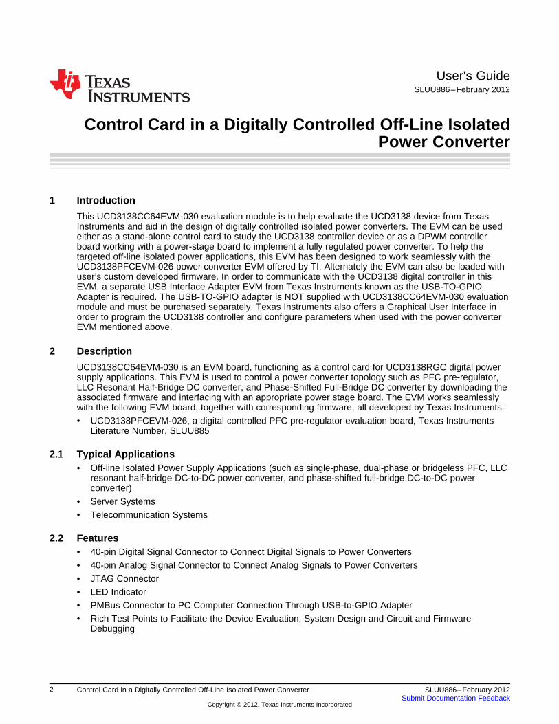
www.ti.com Specifications
3 Specifications
Table 1. UCD3138CC64EVM-030 Specifications
PARAMETER TEST CONDITIONS MIN TYP MAX UNITS
Connector J1
PMBus connector Port of connection to USB-to-GPIO, pin definition refer Standardto TI standard USB-to-GPIO document SLLU093
Connector J2
3.3-V connection to PMBus Port to use on board 3.3 VD to bias PMBus 3.25 3.30 3.35 VDC
Connector J3
Analog signal connection Pin definition in compliance with UCD3138 40-pin
Connector J4
Digital signal connection Pin definition in compliance with UCD3138 40-pin
Pin 39 External voltage source input 11.5 12.0 12.5 VDC
Connector J5
JTAG Standard JTAG communication connection Standard
Connector J6
3.3-V on board to external use Port to use 3.3 V on board to bias external circuit 3.27 3.30 3.32 VDC
Operation Environment
Operating temperature range Natural Convection 25 °C
GUI Accessible Control Variables
Level-1 Not required, standalone operational with preloaded firmware with UCD3138PFCEVM-026
Level-2 GUI accessible, firmware preloaded and used with UCD3138PFCEVM-026
Level-3 Full accessible through user's definition and associated firmware development
PMBus Variables Accessible
Level-1 Not required, stand alone operational with preloaded firmware with UCD3138PFCEVM-026
Level-2 GUI accessible, firmware pre-loaded and used with UCD3138PFCEVM-026
Level-3 Full accessible through user's definition and associated firmware development
MECHANICAL CHARACTERSTICS
Width 1.8
Dimensions Length 3.4 inches
Component height 0.5
3SLUU886–February 2012 Control Card in a Digitally Controlled Off-Line Isolated Power ConverterSubmit Documentation Feedback
Copyright © 2012, Texas Instruments Incorporated
RE
SE
T
Part
snot
used
1
11
11 1
11
11
1
1
11
1
1
1
1
1
1
11
11
1
1
R14
1.5
K
TP2
TP3
TP1
TP6
TP22
TP11
TP23
TP8
TP9
TP10
TP4
TP7
TP16
TP12
TP13
TP14
TP15
TP17
TP18
TP19
TP20
TP21
TP24
TP25
TP26
TP27
TP28
TP29
TP32
TP33
TP34
TP35
TP36
TP30
TP31
1 2 3 4 5 6 7 8 9 10
J1
J2
S1
D1 BAT54A
D2 BAT54A
C31
1000pF
C30
1000pF
C28
1000pF
C29
1000pF
C26
1000pF
C27
1000pF
C24
1000pF
C25
1000pF
C22
1000pF
C23
1000pF
C20
1000pF
C21
1000pF
C18
1000pF
C19
1000pF
C14
1000pF
C7
100pF
C8
1000pF
C17
33pF
C15
33pF
C16
33pF
C9
33pF
C10
33pF
C2
0.1
uF
C3
0.1
uF
C4
0.1
uF
C5
0.1
uF
C6
1uF
C11
0.1
uF
C12
2.2
uF
C1
1uF
C13
0.1
uF
R13
1.5
K
R12
1.6
5K
R9
100
R8
100
R7
100
R5
100
R6 0
R3
R1
R2
R4
R11
16K
R10
10K
R15
100K
R16
100
R17
100
R18
100
R20
100
R19
100
R25
100
R23
100
R26
100
R24
2K
R21
2K
R22
2K
R27
2K
R28
2K
R29
2K
NS1
1AGND
2AD
13
3AD
12
4AD
10
5AD
07
6AD
06
7AD
04
8AD
03
9V33DIO
10DGND
11
RESET
12
AD
C_EXT
13
SCI_
RX0
14
SCI_
TX0
15
PM
BU
S_CLK
16
PM
BU
S_D
ATA
17
DPW
M0A
18
DPW
M0B
19
DPW
M1A
20
DPW
M1B
21
DPW
M2A
22
DPW
M2B
23
DPW
M3A
24
DPW
M3B
25DGND
26
SYN
C
27
PM
BU
S_ALERT
28
PM
BU
S_CTRL
29
SCI_
TX1
30
SCI_
RX1
31
PW
M0
32
PW
M1
33DGND
34
INT_EXT
35
FAU
LT0
36
FAU
LT1
37
TCK
38
TD
O
39
TD
I
40
TM
S
41
TCAP
42
FAU
LT2
43
FAU
LT3
44DGND
45V33DIO
46BP18
47V33D
48AGND
49AGND
50
EAP0
51
EAN
0
52
EAP1
53
EAN
1
54
EAP2
55
EAN
2
56AGND
57V33A
58
AD
00
59
AD
01
60
AD
02
61
AD
05
62
AD
08
63
AD
09
64
AD
11
65
PW
PD
U1
UCD
3138RG
C
TP5
R39
10
AD
-00
SCI-
RX1
SCI-
TX1
SCI-
TX0
SCI-
RX0
EXT-T
RIG
DPW
M-2
B
DPW
M-2
A
DPW
M-1
B
DPW
M-1
A
DPW
M-0
B
DPW
M-0
A
/RESET
TM
S
TD
I
TD
O
TCK
PW
M-1
PW
M-0
AD
-06
AD
-05
AD
-04
AD
-03
AD
-00
EAD
C-N
1
EAD
C-P
1
EAD
C-N
0
DG
ND
AD
-02 AD
-07
DPW
M-3
A
DPW
M-3
B
EAD
C-P
2
EAD
C-N
2
SYN
C
FAU
LT-0
TCAP
AD
-09
AD
-10
AD
-12
AD
-13
EAD
C-P
0
AD
-08
AD
-01
AD
-11
FAU
LT-3
FAU
LT-2
FAU
LT-1
DG
ND
/RESET
DG
ND
INT-E
XT
DG
ND
DG
ND
PM
BU
S-C
TRL
PM
BU
S-C
LK
PM
BU
S-A
LERT
PM
BU
S-D
ATA
3.3
VD
3.3
VD
3.3
VD
3.3
VD
DG
ND
DG
ND
DG
ND
3.3
VA
AG
ND
AG
ND
AG
ND
DG
ND
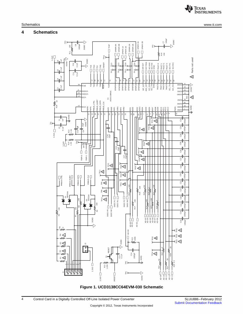
Schematics www.ti.com
4 Schematics
Figure 1. UCD3138CC64EVM-030 Schematic
4 Control Card in a Digitally Controlled Off-Line Isolated Power Converter SLUU886–February 2012Submit Documentation Feedback
Copyright © 2012, Texas Instruments Incorporated
Ifneeded,
use
this
jum
per
topro
vid
e3.3
VD
toapplication
board
1 2 3 4 5 6 7 8 9 10
11
12
13
14
15
16
17
18
19
20
21
22
23
24
25
26
27
28
29
30
31
32
33
34
35
36
37
38
39
40
J3
PPPN
202FJF
N
1 2 3 4 5 6 7 8 9 10
11
12
13
14
15
16
17
18
19
20
21
22
23
24
25
26
27
28
29
30
31
32
33
34
35
36
37
38
39
40
J4
PPPN
202FJF
N
1IN
2N
C
3N
C
4G
ND
5FB/N
C
6N
C
7N
C
8O
UT
9PWPD
U2
TPS715A33D
RBR
TP37
C33
10uF
C32
1uF
R31
301
R30
0.5
R35
10K
R32
10K
R33
10K
R37
10K
R38
10K
R34 0
R36 0
D3
J6
1 2 3 4 5 6 7 8 910
11
12
13
14
J5
C34
0.1
uF
EAD
C-N
2
EAD
C-N
1
EAD
C-N
0
EAD
C-P
0
EAD
C-P
1
EAD
C-P
2
AD
-00
AD
-01
AD
-02
AD
-03
AD
-04
AD
-05
AD
-06
AD
-07
AD
-08
AD
-09
AD
-10
AD
-11
AD
-12
AD
-13
DPW
M-0
A
DPW
M-1
A
DPW
M-2
A
DPW
M-3
A
FAU
LT-0
SYN
C
FAU
LT-2
SCI-
TX1
PW
M-0
TCAP
SCI-
TX0
INT-E
XT
+12V_EXT
DPW
M-0
B
DPW
M-1
B
DPW
M-2
B
DPW
M-3
B
FAU
LT-3
SCI-
RX1
PW
M-1
SCI-
RX0
EXT-T
RIG
/RESET
3.3
VD
TM
S
TD
I
TD
O
TCK
DG
ND
+12V_EXT
FAU
LT-1
3.3
VD
3.3
VD
3.3
VD
DG
ND
DG
ND
AG
ND
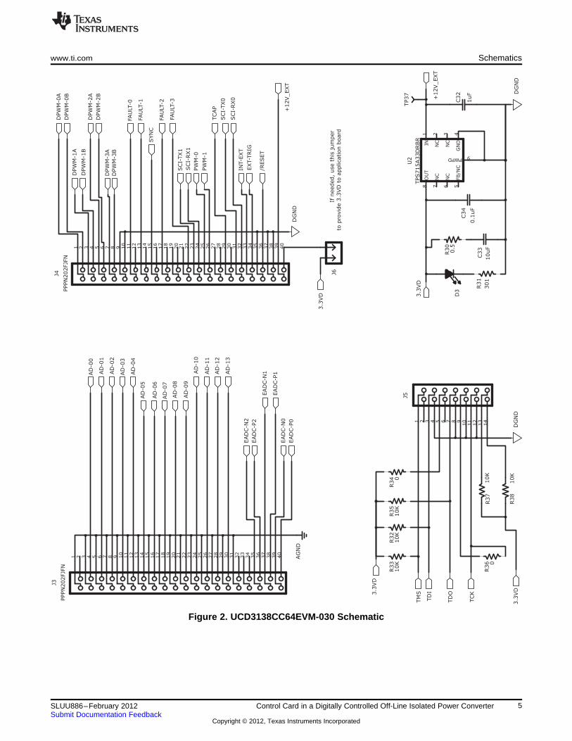
www.ti.com Schematics
Figure 2. UCD3138CC64EVM-030 Schematic
5SLUU886–February 2012 Control Card in a Digitally Controlled Off-Line Isolated Power ConverterSubmit Documentation Feedback
Copyright © 2012, Texas Instruments Incorporated
Test Equipment www.ti.com
5 Test Equipment
5.1 PC Computer
5.1.1 Operating System
Microsoft Windows XP (32 bit), or Vista (32 bit), or Windows 7 (32 bit).
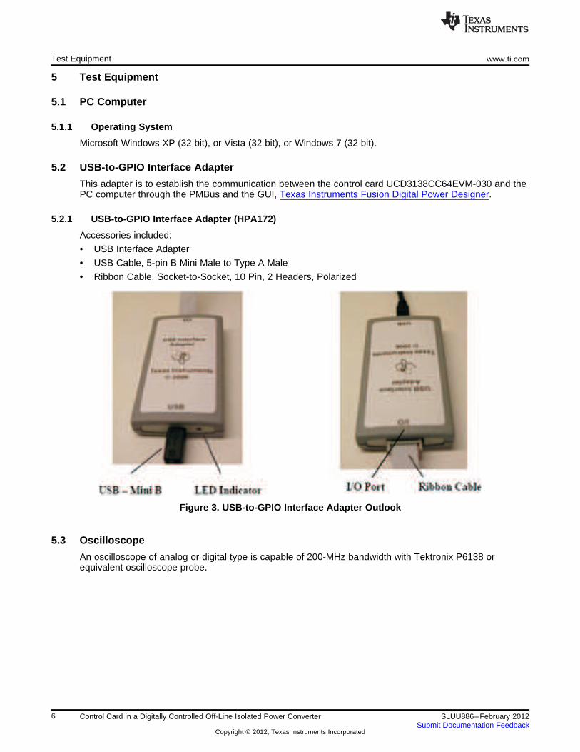
5.2 USB-to-GPIO Interface Adapter
This adapter is to establish the communication between the control card UCD3138CC64EVM-030 and thePC computer through the PMBus and the GUI, Texas Instruments Fusion Digital Power Designer.
5.2.1 USB-to-GPIO Interface Adapter (HPA172)
Accessories included:
• USB Interface Adapter
• USB Cable, 5-pin B Mini Male to Type A Male
• Ribbon Cable, Socket-to-Socket, 10 Pin, 2 Headers, Polarized
Figure 3. USB-to-GPIO Interface Adapter Outlook
5.3 Oscilloscope
An oscilloscope of analog or digital type is capable of 200-MHz bandwidth with Tektronix P6138 orequivalent oscilloscope probe.
6 Control Card in a Digitally Controlled Off-Line Isolated Power Converter SLUU886–February 2012Submit Documentation Feedback
Copyright © 2012, Texas Instruments Incorporated
www.ti.com Equipment Setup
6 Equipment Setup
6.1 GUI (Graphical User Interface)
6.1.1 File for Installation
The GUI installation file is TI-Fusion-Digital-Power-Designer-Version-1.8.92.exe or newer version. To get alatest version of GUI, go on TI web site, www.ti.com, Texas Instruments Fusion Digital Power Designerdownload and install to one’s computer.
6.1.2 Installation
Double click and launch the .exe file to start the installation. Click Next all the way through. When present,click I accept the agreement after read it. Then click install. After the installation, click Finish to exit setup.Then click Exit Program.
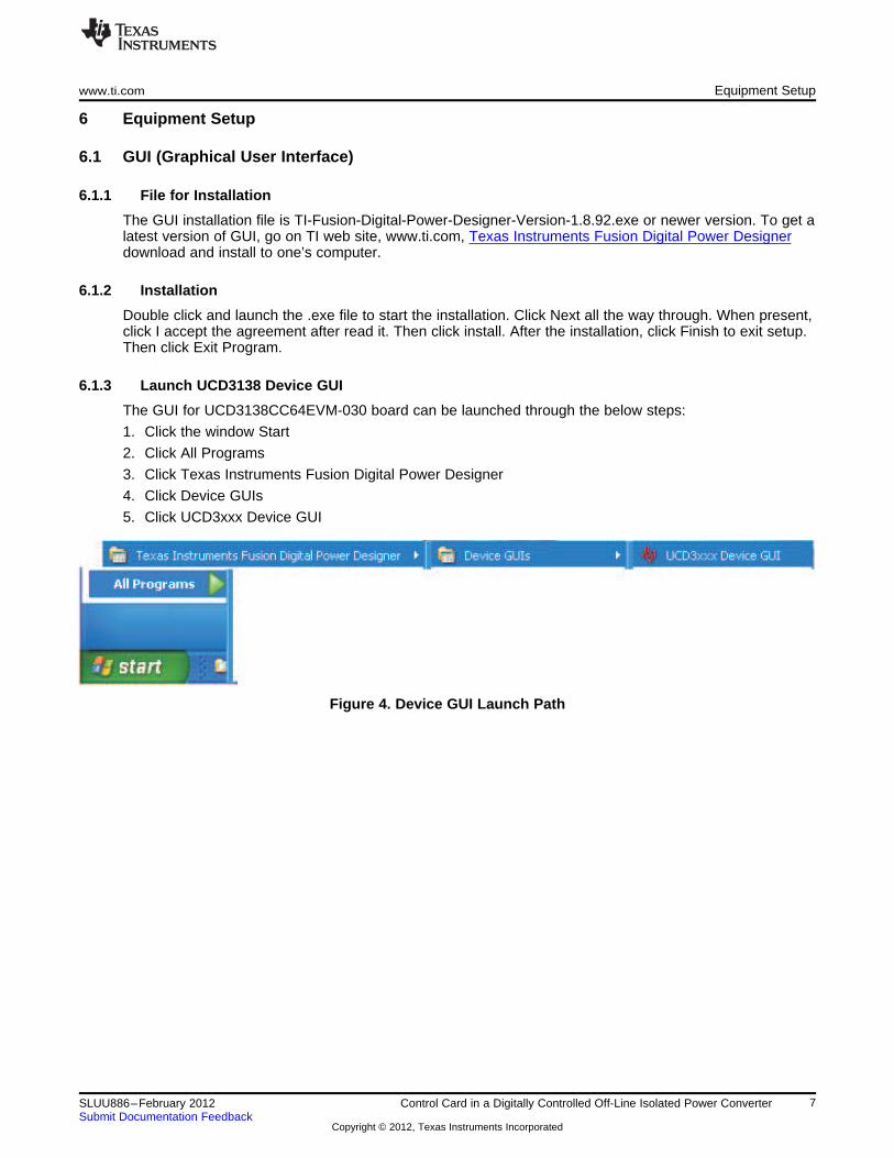
6.1.3 Launch UCD3138 Device GUI
The GUI for UCD3138CC64EVM-030 board can be launched through the below steps:
1. Click the window Start
2. Click All Programs
3. Click Texas Instruments Fusion Digital Power Designer
4. Click Device GUIs
5. Click UCD3xxx Device GUI
Figure 4. Device GUI Launch Path
7SLUU886–February 2012 Control Card in a Digitally Controlled Off-Line Isolated Power ConverterSubmit Documentation Feedback
Copyright © 2012, Texas Instruments Incorporated
Equipment Setup www.ti.com
6.2 Hardware Setup
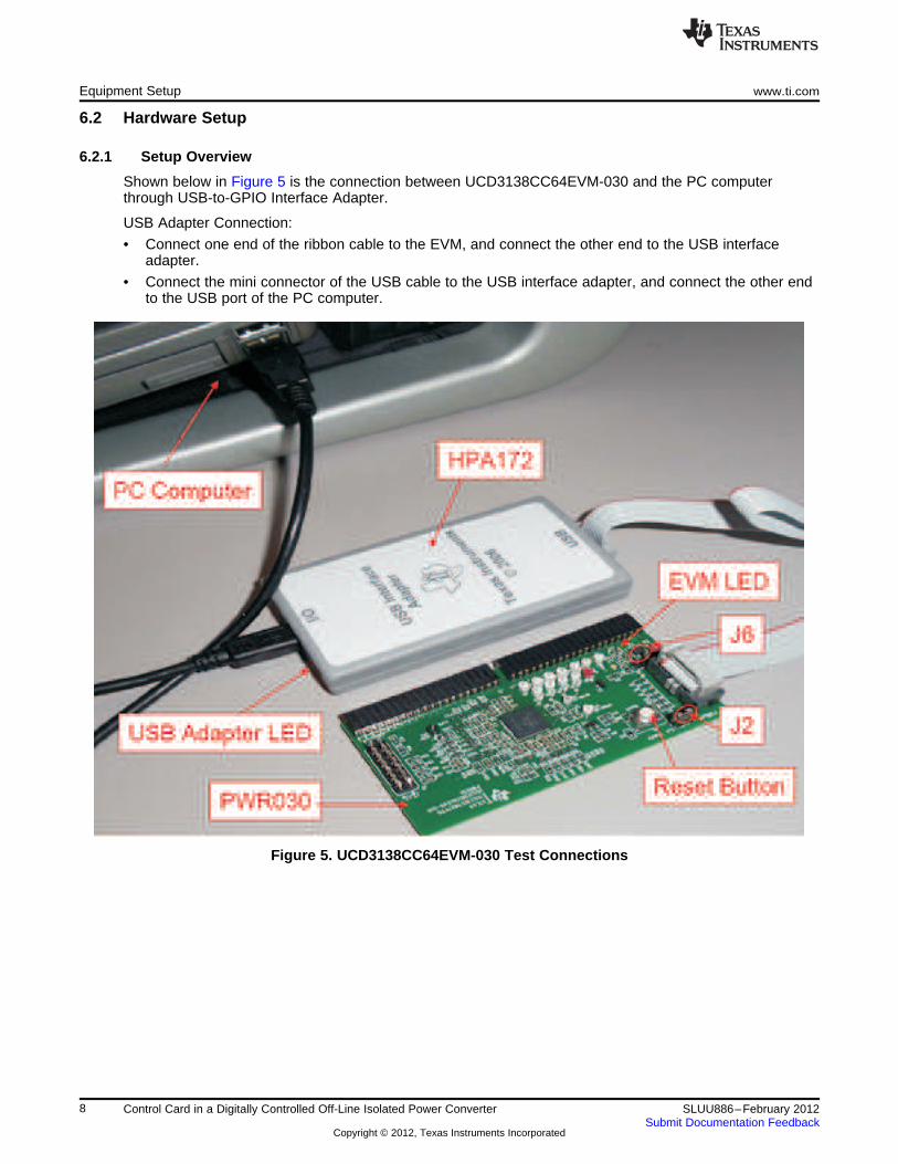
6.2.1 Setup Overview
Shown below in Figure 5 is the connection between UCD3138CC64EVM-030 and the PC computerthrough USB-to-GPIO Interface Adapter.
USB Adapter Connection:
• Connect one end of the ribbon cable to the EVM, and connect the other end to the USB interfaceadapter.
• Connect the mini connector of the USB cable to the USB interface adapter, and connect the other endto the USB port of the PC computer.
Figure 5. UCD3138CC64EVM-030 Test Connections
8 Control Card in a Digitally Controlled Off-Line Isolated Power Converter SLUU886–February 2012Submit Documentation Feedback
Copyright © 2012, Texas Instruments Incorporated
www.ti.com Equipment Setup
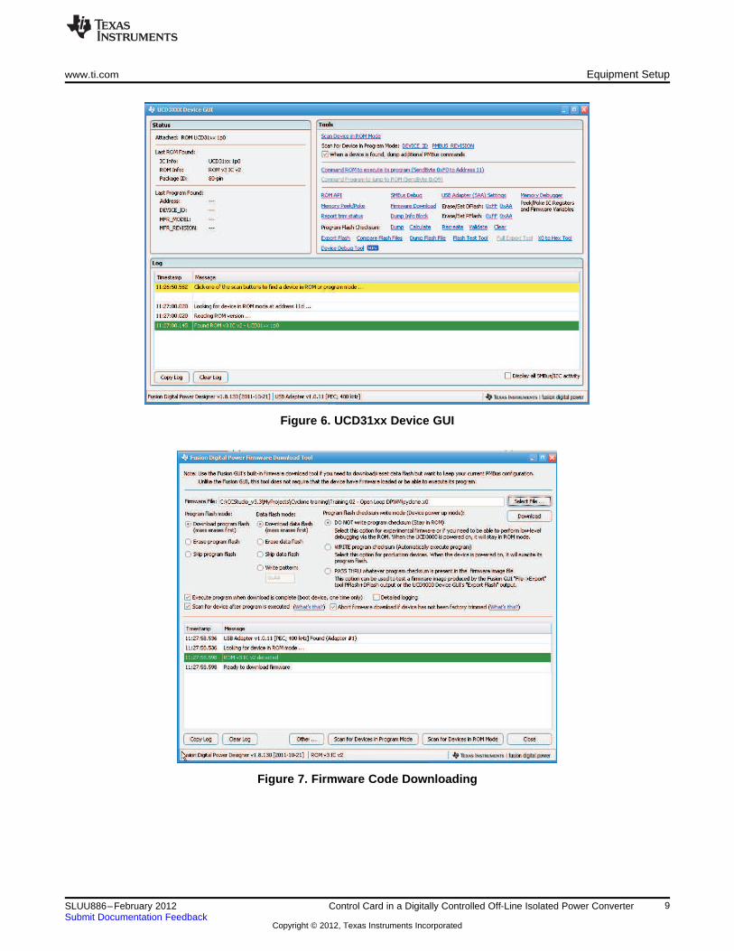
Figure 6. UCD31xx Device GUI
Figure 7. Firmware Code Downloading
9SLUU886–February 2012 Control Card in a Digitally Controlled Off-Line Isolated Power ConverterSubmit Documentation Feedback
Copyright © 2012, Texas Instruments Incorporated
Equipment Setup www.ti.com
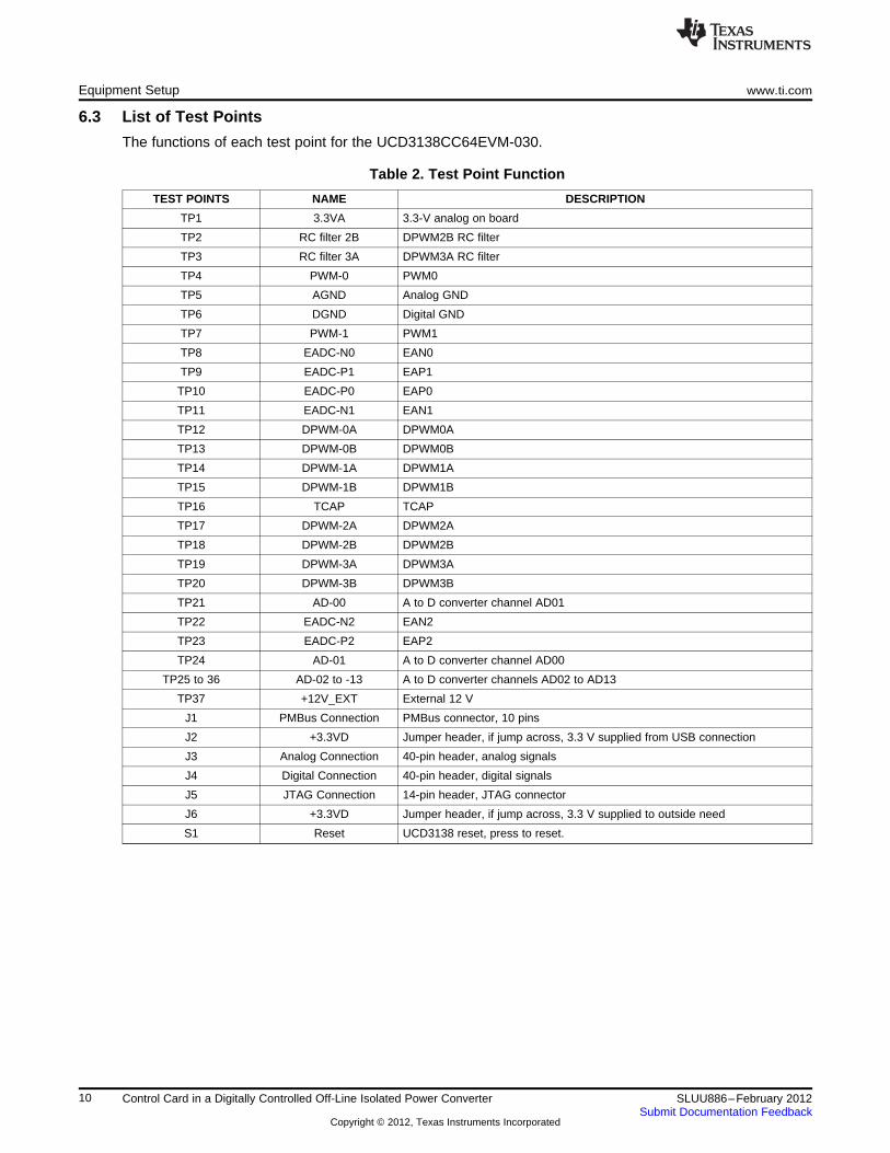
6.3 List of Test Points
The functions of each test point for the UCD3138CC64EVM-030.
Table 2. Test Point Function
TEST POINTS NAME DESCRIPTION
TP1 3.3VA 3.3-V analog on board
TP2 RC filter 2B DPWM2B RC filter
TP3 RC filter 3A DPWM3A RC filter
TP4 PWM-0 PWM0
TP5 AGND Analog GND
TP6 DGND Digital GND
TP7 PWM-1 PWM1
TP8 EADC-N0 EAN0
TP9 EADC-P1 EAP1
TP10 EADC-P0 EAP0
TP11 EADC-N1 EAN1
TP12 DPWM-0A DPWM0A
TP13 DPWM-0B DPWM0B
TP14 DPWM-1A DPWM1A
TP15 DPWM-1B DPWM1B
TP16 TCAP TCAP
TP17 DPWM-2A DPWM2A
TP18 DPWM-2B DPWM2B
TP19 DPWM-3A DPWM3A
TP20 DPWM-3B DPWM3B
TP21 AD-00 A to D converter channel AD01
TP22 EADC-N2 EAN2
TP23 EADC-P2 EAP2
TP24 AD-01 A to D converter channel AD00
TP25 to 36 AD-02 to -13 A to D converter channels AD02 to AD13
TP37 +12V_EXT External 12 V
J1 PMBus Connection PMBus connector, 10 pins
J2 +3.3VD Jumper header, if jump across, 3.3 V supplied from USB connection
J3 Analog Connection 40-pin header, analog signals
J4 Digital Connection 40-pin header, digital signals
J5 JTAG Connection 14-pin header, JTAG connector
J6 +3.3VD Jumper header, if jump across, 3.3 V supplied to outside need
S1 Reset UCD3138 reset, press to reset.
10 Control Card in a Digitally Controlled Off-Line Isolated Power Converter SLUU886–February 2012Submit Documentation Feedback
Copyright © 2012, Texas Instruments Incorporated
www.ti.com Test Procedure
7 Test Procedure
7.1 Download Firmware Codes to UCD3138CC64EVM-030
Set up the EVM connection based on Figure 5.
1. Set up the EVM connection based on Figure 5. The LED of USB adapter is lighted up.
2. Use provided jumper jump across J2. The LED of the EVM is lighted up.
3. Launch the UCD31xx device GUI following the steps described in 6.1.3. A window shown in Figure 6appears.
4. Click Firmware Download; then a new window appears as shown in Figure 7. Click Select File andbrowse an intended firmware code file with file extension .x0, for example, cyclone.x0; then clickDownload. The firmware of cyclone.x0 is being downloaded to the device UCD3138 on the board ofUCD3138CC64EVM-030. When asking, click yes to complete the download. Click Close to exit thedownload window.
5. After the firmware codes downloaded to the UCD3138 device, the intended test can be performed. Forexample, with the provided firmware cyclone.x0, one can observe voltage toggled between 0 V and 3.3V on test point TP7.
7.2 Erase Firmware Codes from UCD3138CC64EVM-030
Erasing the downloaded firmware codes from UCD3138 flash memory can be made with the steps belowbased on Figure 6.
1. Click Device ID
2. Click Command Program to jump to ROM (SendByte.0xD9)
3. Click Erase/Set PFlash: 0xFF
7.3 Equipment Shutdown1. Exit the GUI
2. Disconnect the USB cable and the ribbon cable
11SLUU886–February 2012 Control Card in a Digitally Controlled Off-Line Isolated Power ConverterSubmit Documentation Feedback
Copyright © 2012, Texas Instruments Incorporated
EVM Assembly Drawing and PCB layout www.ti.com
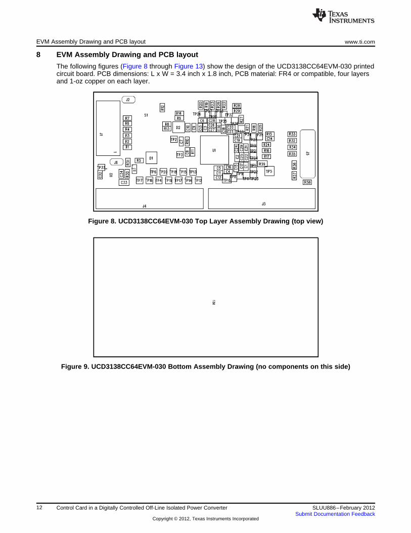
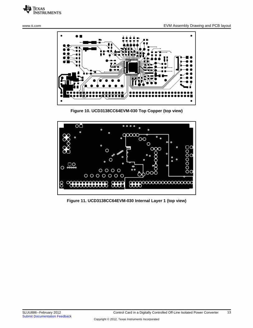
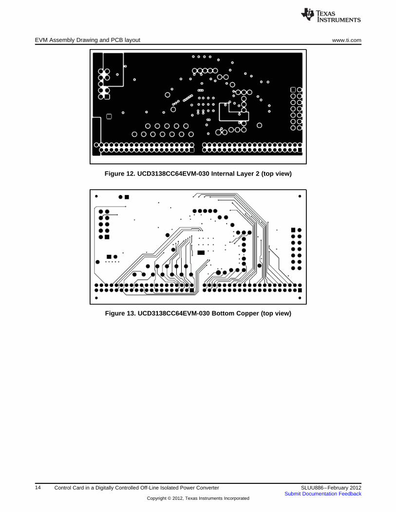
8 EVM Assembly Drawing and PCB layout
The following figures (Figure 8 through Figure 13) show the design of the UCD3138CC64EVM-030 printedcircuit board. PCB dimensions: L x W = 3.4 inch x 1.8 inch, PCB material: FR4 or compatible, four layersand 1-oz copper on each layer.
Figure 8. UCD3138CC64EVM-030 Top Layer Assembly Drawing (top view)
Figure 9. UCD3138CC64EVM-030 Bottom Assembly Drawing (no components on this side)
12 Control Card in a Digitally Controlled Off-Line Isolated Power Converter SLUU886–February 2012Submit Documentation Feedback
Copyright © 2012, Texas Instruments Incorporated
www.ti.com EVM Assembly Drawing and PCB layout
Figure 10. UCD3138CC64EVM-030 Top Copper (top view)
Figure 11. UCD3138CC64EVM-030 Internal Layer 1 (top view)
13SLUU886–February 2012 Control Card in a Digitally Controlled Off-Line Isolated Power ConverterSubmit Documentation Feedback
Copyright © 2012, Texas Instruments Incorporated
EVM Assembly Drawing and PCB layout www.ti.com
Figure 12. UCD3138CC64EVM-030 Internal Layer 2 (top view)
Figure 13. UCD3138CC64EVM-030 Bottom Copper (top view)
14 Control Card in a Digitally Controlled Off-Line Isolated Power Converter SLUU886–February 2012Submit Documentation Feedback
Copyright © 2012, Texas Instruments Incorporated
www.ti.com List of Materials
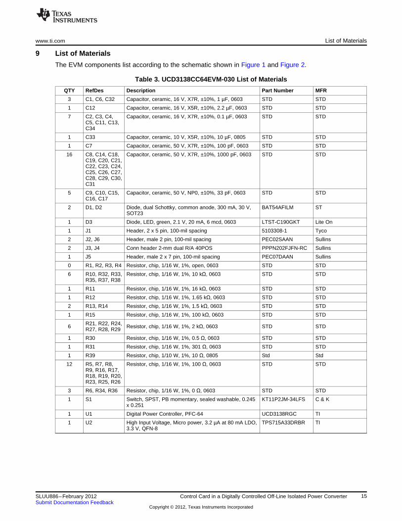
9 List of Materials
The EVM components list according to the schematic shown in Figure 1 and Figure 2.
Table 3. UCD3138CC64EVM-030 List of Materials
QTY RefDes Description Part Number MFR
3 C1, C6, C32 Capacitor, ceramic, 16 V, X7R, ±10%, 1 µF, 0603 STD STD
1 C12 Capacitor, ceramic, 16 V, X5R, ±10%, 2.2 µF, 0603 STD STD
7 C2, C3, C4, Capacitor, ceramic, 16 V, X7R, ±10%, 0.1 µF, 0603 STD STDC5, C11, C13,C34
1 C33 Capacitor, ceramic, 10 V, X5R, ±10%, 10 µF, 0805 STD STD
1 C7 Capacitor, ceramic, 50 V, X7R, ±10%, 100 pF, 0603 STD STD
16 C8, C14, C18, Capacitor, ceramic, 50 V, X7R, ±10%, 1000 pF, 0603 STD STDC19, C20, C21,C22, C23, C24,C25, C26, C27,C28, C29, C30,C31
5 C9, C10, C15, Capacitor, ceramic, 50 V, NP0, ±10%, 33 pF, 0603 STD STDC16, C17
2 D1, D2 Diode, dual Schottky, common anode, 300 mA, 30 V, BAT54AFILM STSOT23
1 D3 Diode, LED, green, 2.1 V, 20 mA, 6 mcd, 0603 LTST-C190GKT Lite On
1 J1 Header, 2 x 5 pin, 100-mil spacing 5103308-1 Tyco
2 J2, J6 Header, male 2 pin, 100-mil spacing PEC02SAAN Sullins
2 J3, J4 Conn header 2-mm dual R/A 40POS PPPN202FJFN-RC Sullins
1 J5 Header, male 2 x 7 pin, 100-mil spacing PEC07DAAN Sullins
0 R1, R2, R3, R4 Resistor, chip, 1/16 W, 1%, open, 0603 STD STD
6 R10, R32, R33, Resistor, chip, 1/16 W, 1%, 10 kΩ, 0603 STD STDR35, R37, R38
1 R11 Resistor, chip, 1/16 W, 1%, 16 kΩ, 0603 STD STD
1 R12 Resistor, chip, 1/16 W, 1%, 1.65 kΩ, 0603 STD STD
2 R13, R14 Resistor, chip, 1/16 W, 1%, 1.5 kΩ, 0603 STD STD
1 R15 Resistor, chip, 1/16 W, 1%, 100 kΩ, 0603 STD STD
R21, R22, R24,6 Resistor, chip, 1/16 W, 1%, 2 kΩ, 0603 STD STDR27, R28, R29
1 R30 Resistor, chip, 1/16 W, 1%, 0.5 Ω, 0603 STD STD
1 R31 Resistor, chip, 1/16 W, 1%, 301 Ω, 0603 STD STD
1 R39 Resistor, chip, 1/10 W, 1%, 10 Ω, 0805 Std Std
12 R5, R7, R8, Resistor, chip, 1/16 W, 1%, 100 Ω, 0603 STD STDR9, R16, R17,R18, R19, R20,R23, R25, R26
3 R6, R34, R36 Resistor, chip, 1/16 W, 1%, 0 Ω, 0603 STD STD
1 S1 Switch, SPST, PB momentary, sealed washable, 0.245 KT11P2JM-34LFS C & Kx 0.251
1 U1 Digital Power Controller, PFC-64 UCD3138RGC TI
1 U2 High Input Voltage, Micro power, 3.2 µA at 80 mA LDO, TPS715A33DRBR TI3.3 V, QFN-8
15SLUU886–February 2012 Control Card in a Digitally Controlled Off-Line Isolated Power ConverterSubmit Documentation Feedback
Copyright © 2012, Texas Instruments Incorporated
www.ti.com
Appendix A Summary of Using Code Composer Studio v3.3
Described in this appendix are basic steps on how to use Code Composer Studio v3.3, or CCS, tocompile firmware for UCD3138. A design flow is described while detailed steps for firmware code creation,and firmware debugging.
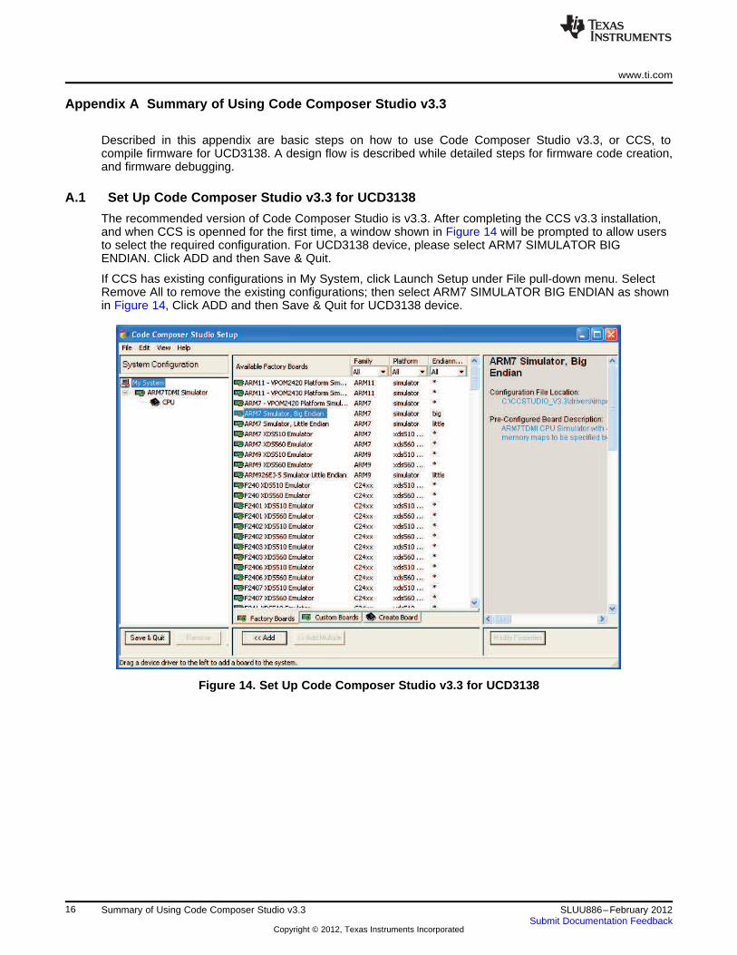
A.1 Set Up Code Composer Studio v3.3 for UCD3138
The recommended version of Code Composer Studio is v3.3. After completing the CCS v3.3 installation,and when CCS is openned for the first time, a window shown in Figure 14 will be prompted to allow usersto select the required configuration. For UCD3138 device, please select ARM7 SIMULATOR BIGENDIAN. Click ADD and then Save & Quit.
If CCS has existing configurations in My System, click Launch Setup under File pull-down menu. SelectRemove All to remove the existing configurations; then select ARM7 SIMULATOR BIG ENDIAN as shownin Figure 14, Click ADD and then Save & Quit for UCD3138 device.
Figure 14. Set Up Code Composer Studio v3.3 for UCD3138
16 Summary of Using Code Composer Studio v3.3 SLUU886–February 2012Submit Documentation Feedback
Copyright © 2012, Texas Instruments Incorporated
www.ti.com Build/Compile a Project Using Code Composer Studio
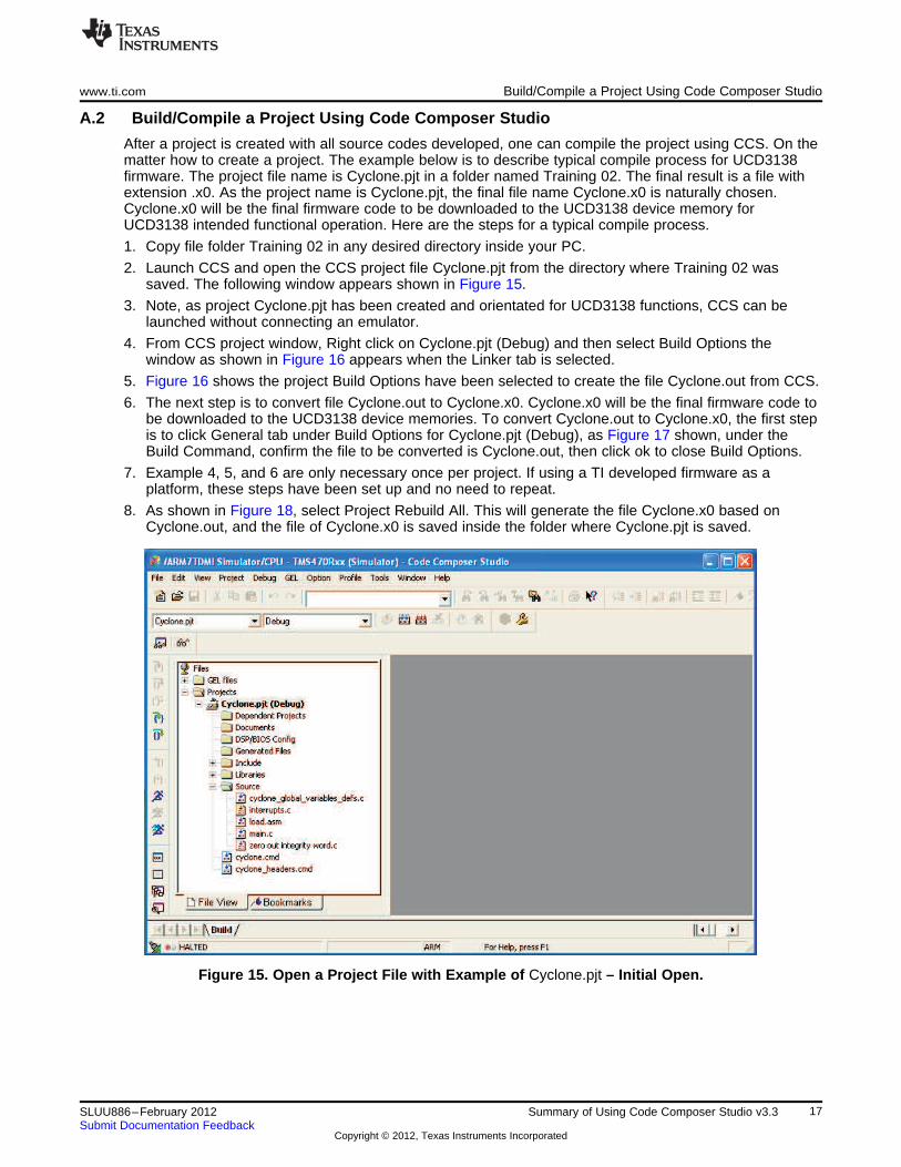
A.2 Build/Compile a Project Using Code Composer Studio
After a project is created with all source codes developed, one can compile the project using CCS. On thematter how to create a project. The example below is to describe typical compile process for UCD3138firmware. The project file name is Cyclone.pjt in a folder named Training 02. The final result is a file withextension .x0. As the project name is Cyclone.pjt, the final file name Cyclone.x0 is naturally chosen.Cyclone.x0 will be the final firmware code to be downloaded to the UCD3138 device memory forUCD3138 intended functional operation. Here are the steps for a typical compile process.
1. Copy file folder Training 02 in any desired directory inside your PC.
2. Launch CCS and open the CCS project file Cyclone.pjt from the directory where Training 02 wassaved. The following window appears shown in Figure 15.
3. Note, as project Cyclone.pjt has been created and orientated for UCD3138 functions, CCS can belaunched without connecting an emulator.
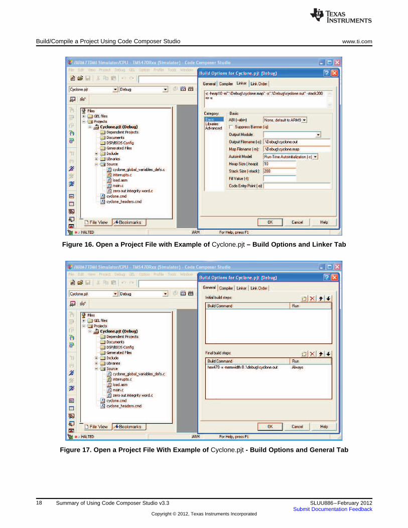
4. From CCS project window, Right click on Cyclone.pjt (Debug) and then select Build Options thewindow as shown in Figure 16 appears when the Linker tab is selected.
5. Figure 16 shows the project Build Options have been selected to create the file Cyclone.out from CCS.
6. The next step is to convert file Cyclone.out to Cyclone.x0. Cyclone.x0 will be the final firmware code tobe downloaded to the UCD3138 device memories. To convert Cyclone.out to Cyclone.x0, the first stepis to click General tab under Build Options for Cyclone.pjt (Debug), as Figure 17 shown, under theBuild Command, confirm the file to be converted is Cyclone.out, then click ok to close Build Options.
7. Example 4, 5, and 6 are only necessary once per project. If using a TI developed firmware as aplatform, these steps have been set up and no need to repeat.
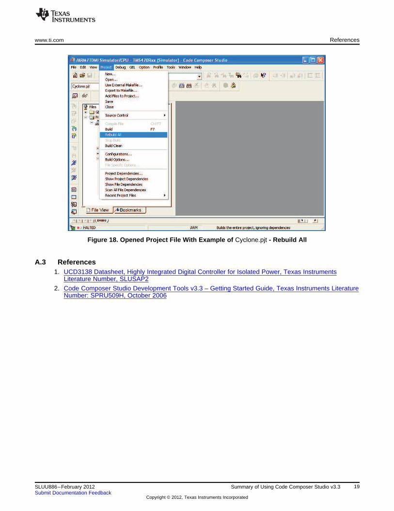
8. As shown in Figure 18, select Project Rebuild All. This will generate the file Cyclone.x0 based onCyclone.out, and the file of Cyclone.x0 is saved inside the folder where Cyclone.pjt is saved.
Figure 15. Open a Project File with Example of Cyclone.pjt – Initial Open.
17SLUU886–February 2012 Summary of Using Code Composer Studio v3.3Submit Documentation Feedback
Copyright © 2012, Texas Instruments Incorporated
Build/Compile a Project Using Code Composer Studio www.ti.com
Figure 16. Open a Project File with Example of Cyclone.pjt – Build Options and Linker Tab
Figure 17. Open a Project File With Example of Cyclone.pjt - Build Options and General Tab
18 Summary of Using Code Composer Studio v3.3 SLUU886–February 2012Submit Documentation Feedback
Copyright © 2012, Texas Instruments Incorporated
www.ti.com References
Figure 18. Opened Project File With Example of Cyclone.pjt - Rebuild All
A.3 References1. UCD3138 Datasheet, Highly Integrated Digital Controller for Isolated Power, Texas Instruments
Literature Number, SLUSAP2
2. Code Composer Studio Development Tools v3.3 – Getting Started Guide, Texas Instruments LiteratureNumber: SPRU509H, October 2006
19SLUU886–February 2012 Summary of Using Code Composer Studio v3.3Submit Documentation Feedback
Copyright © 2012, Texas Instruments Incorporated
Evaluation Board/Kit Important Notice
Texas Instruments (TI) provides the enclosed product(s) under the following conditions:
This evaluation board/kit is intended for use for ENGINEERING DEVELOPMENT, DEMONSTRATION, OR EVALUATIONPURPOSES ONLY and is not considered by TI to be a finished end-product fit for general consumer use. Persons handling theproduct(s) must have electronics training and observe good engineering practice standards. As such, the goods being provided arenot intended to be complete in terms of required design-, marketing-, and/or manufacturing-related protective considerations,including product safety and environmental measures typically found in end products that incorporate such semiconductorcomponents or circuit boards. This evaluation board/kit does not fall within the scope of the European Union directives regardingelectromagnetic compatibility, restricted substances (RoHS), recycling (WEEE), FCC, CE or UL, and therefore may not meet thetechnical requirements of these directives or other related directives.
Should this evaluation board/kit not meet the specifications indicated in the User’s Guide, the board/kit may be returned within 30days from the date of delivery for a full refund. THE FOREGOING WARRANTY IS THE EXCLUSIVE WARRANTY MADE BYSELLER TO BUYER AND IS IN LIEU OF ALL OTHER WARRANTIES, EXPRESSED, IMPLIED, OR STATUTORY, INCLUDINGANY WARRANTY OF MERCHANTABILITY OR FITNESS FOR ANY PARTICULAR PURPOSE.
The user assumes all responsibility and liability for proper and safe handling of the goods. Further, the user indemnifies TI from allclaims arising from the handling or use of the goods. Due to the open construction of the product, it is the user’s responsibility totake any and all appropriate precautions with regard to electrostatic discharge.
EXCEPT TO THE EXTENT OF THE INDEMNITY SET FORTH ABOVE, NEITHER PARTY SHALL BE LIABLE TO THE OTHERFOR ANY INDIRECT, SPECIAL, INCIDENTAL, OR CONSEQUENTIAL DAMAGES.
TI currently deals with a variety of customers for products, and therefore our arrangement with the user is not exclusive.
TI assumes no liability for applications assistance, customer product design, software performance, or infringement ofpatents or services described herein.
Please read the User’s Guide and, specifically, the Warnings and Restrictions notice in the User’s Guide prior to handling theproduct. This notice contains important safety information about temperatures and voltages. For additional information on TI’senvironmental and/or safety programs, please contact the TI application engineer or visit www.ti.com/esh.
No license is granted under any patent right or other intellectual property right of TI covering or relating to any machine, process, orcombination in which such TI products or services might be or are used.
FCC Warning
This evaluation board/kit is intended for use for ENGINEERING DEVELOPMENT, DEMONSTRATION, OR EVALUATIONPURPOSES ONLY and is not considered by TI to be a finished end-product fit for general consumer use. It generates, uses, andcan radiate radio frequency energy and has not been tested for compliance with the limits of computing devices pursuant to part 15of FCC rules, which are designed to provide reasonable protection against radio frequency interference. Operation of thisequipment in other environments may cause interference with radio communications, in which case the user at his own expensewill be required to take whatever measures may be required to correct this interference.
EVM Warnings and Restrictions
It is important to operate this EVM within the input voltage range of 0 V to 3 V and the output voltage range of 0 V to 3 V.
Exceeding the specified input range may cause unexpected operation and/or irreversible damage to the EVM. If there arequestions concerning the input range, please contact a TI field representative prior to connecting the input power.
Applying loads outside of the specified output range may result in unintended operation and/or possible permanent damage to theEVM. Please consult the EVM User's Guide prior to connecting any load to the EVM output. If there is uncertainty as to the loadspecification, please contact a TI field representative.
During normal operation, some circuit components may have case temperatures greater than 25°C. The EVM is designed tooperate properly with certain components above 25°C as long as the input and output ranges are maintained. These componentsinclude but are not limited to linear regulators, switching transistors, pass transistors, and current sense resistors. These types ofdevices can be identified using the EVM schematic located in the EVM User's Guide. When placing measurement probes nearthese devices during operation, please be aware that these devices may be very warm to the touch.
Mailing Address: Texas Instruments, Post Office Box 655303, Dallas, Texas 75265Copyright © 2012, Texas Instruments Incorporated
EVALUATION BOARD/KIT/MODULE (EVM) ADDITIONAL TERMSTexas Instruments (TI) provides the enclosed Evaluation Board/Kit/Module (EVM) under the following conditions:
The user assumes all responsibility and liability for proper and safe handling of the goods. Further, the user indemnifies TI from all claimsarising from the handling or use of the goods.
Should this evaluation board/kit not meet the specifications indicated in the User’s Guide, the board/kit may be returned within 30 days fromthe date of delivery for a full refund. THE FOREGOING LIMITED WARRANTY IS THE EXCLUSIVE WARRANTY MADE BY SELLER TOBUYER AND IS IN LIEU OF ALL OTHER WARRANTIES, EXPRESSED, IMPLIED, OR STATUTORY, INCLUDING ANY WARRANTY OFMERCHANTABILITY OR FITNESS FOR ANY PARTICULAR PURPOSE. EXCEPT TO THE EXTENT OF THE INDEMNITY SET FORTHABOVE, NEITHER PARTY SHALL BE LIABLE TO THE OTHER FOR ANY INDIRECT, SPECIAL, INCIDENTAL, OR CONSEQUENTIALDAMAGES.
Please read the User's Guide and, specifically, the Warnings and Restrictions notice in the User's Guide prior to handling the product. Thisnotice contains important safety information about temperatures and voltages. For additional information on TI's environmental and/or safetyprograms, please visit www.ti.com/esh or contact TI.
No license is granted under any patent right or other intellectual property right of TI covering or relating to any machine, process, orcombination in which such TI products or services might be or are used. TI currently deals with a variety of customers for products, andtherefore our arrangement with the user is not exclusive. TI assumes no liability for applications assistance, customer product design,software performance, or infringement of patents or services described herein.
REGULATORY COMPLIANCE INFORMATIONAs noted in the EVM User’s Guide and/or EVM itself, this EVM and/or accompanying hardware may or may not be subject to the FederalCommunications Commission (FCC) and Industry Canada (IC) rules.
For EVMs not subject to the above rules, this evaluation board/kit/module is intended for use for ENGINEERING DEVELOPMENT,DEMONSTRATION OR EVALUATION PURPOSES ONLY and is not considered by TI to be a finished end product fit for general consumeruse. It generates, uses, and can radiate radio frequency energy and has not been tested for compliance with the limits of computingdevices pursuant to part 15 of FCC or ICES-003 rules, which are designed to provide reasonable protection against radio frequencyinterference. Operation of the equipment may cause interference with radio communications, in which case the user at his own expense willbe required to take whatever measures may be required to correct this interference.
General Statement for EVMs including a radioUser Power/Frequency Use Obligations: This radio is intended for development/professional use only in legally allocated frequency andpower limits. Any use of radio frequencies and/or power availability of this EVM and its development application(s) must comply with locallaws governing radio spectrum allocation and power limits for this evaluation module. It is the user’s sole responsibility to only operate thisradio in legally acceptable frequency space and within legally mandated power limitations. Any exceptions to this are strictly prohibited andunauthorized by Texas Instruments unless user has obtained appropriate experimental/development licenses from local regulatoryauthorities, which is responsibility of user including its acceptable authorization.
For EVMs annotated as FCC – FEDERAL COMMUNICATIONS COMMISSION Part 15 Compliant
CautionThis device complies with part 15 of the FCC Rules. Operation is subject to the following two conditions: (1) This device may not causeharmful interference, and (2) this device must accept any interference received, including interference that may cause undesired operation.
Changes or modifications not expressly approved by the party responsible for compliance could void the user's authority to operate theequipment.
FCC Interference Statement for Class A EVM devicesThis equipment has been tested and found to comply with the limits for a Class A digital device, pursuant to part 15 of the FCC Rules.These limits are designed to provide reasonable protection against harmful interference when the equipment is operated in a commercialenvironment. This equipment generates, uses, and can radiate radio frequency energy and, if not installed and used in accordance with theinstruction manual, may cause harmful interference to radio communications. Operation of this equipment in a residential area is likely tocause harmful interference in which case the user will be required to correct the interference at his own expense.
FCC Interference Statement for Class B EVM devicesThis equipment has been tested and found to comply with the limits for a Class B digital device, pursuant to part 15 of the FCC Rules.These limits are designed to provide reasonable protection against harmful interference in a residential installation. This equipmentgenerates, uses and can radiate radio frequency energy and, if not installed and used in accordance with the instructions, may causeharmful interference to radio communications. However, there is no guarantee that interference will not occur in a particular installation. Ifthis equipment does cause harmful interference to radio or television reception, which can be determined by turning the equipment off andon, the user is encouraged to try to correct the interference by one or more of the following measures:
• Reorient or relocate the receiving antenna.• Increase the separation between the equipment and receiver.• Connect the equipment into an outlet on a circuit different from that to which the receiver is connected.• Consult the dealer or an experienced radio/TV technician for help.
For EVMs annotated as IC – INDUSTRY CANADA Compliant
This Class A or B digital apparatus complies with Canadian ICES-003.
Changes or modifications not expressly approved by the party responsible for compliance could void the user’s authority to operate theequipment.
Concerning EVMs including radio transmitters
This device complies with Industry Canada licence-exempt RSS standard(s). Operation is subject to the following two conditions: (1) thisdevice may not cause interference, and (2) this device must accept any interference, including interference that may cause undesiredoperation of the device.
Concerning EVMs including detachable antennasUnder Industry Canada regulations, this radio transmitter may only operate using an antenna of a type and maximum (or lesser) gainapproved for the transmitter by Industry Canada. To reduce potential radio interference to other users, the antenna type and its gain shouldbe so chosen that the equivalent isotropically radiated power (e.i.r.p.) is not more than that necessary for successful communication.
This radio transmitter has been approved by Industry Canada to operate with the antenna types listed in the user guide with the maximumpermissible gain and required antenna impedance for each antenna type indicated. Antenna types not included in this list, having a gaingreater than the maximum gain indicated for that type, are strictly prohibited for use with this device.
Cet appareil numérique de la classe A ou B est conforme à la norme NMB-003 du Canada.
Les changements ou les modifications pas expressément approuvés par la partie responsable de la conformité ont pu vider l’autorité del'utilisateur pour actionner l'équipement.
Concernant les EVMs avec appareils radio
Le présent appareil est conforme aux CNR d'Industrie Canada applicables aux appareils radio exempts de licence. L'exploitation estautorisée aux deux conditions suivantes : (1) l'appareil ne doit pas produire de brouillage, et (2) l'utilisateur de l'appareil doit accepter toutbrouillage radioélectrique subi, même si le brouillage est susceptible d'en compromettre le fonctionnement.
Concernant les EVMs avec antennes détachables
Conformément à la réglementation d'Industrie Canada, le présent émetteur radio peut fonctionner avec une antenne d'un type et d'un gainmaximal (ou inférieur) approuvé pour l'émetteur par Industrie Canada. Dans le but de réduire les risques de brouillage radioélectrique àl'intention des autres utilisateurs, il faut choisir le type d'antenne et son gain de sorte que la puissance isotrope rayonnée équivalente(p.i.r.e.) ne dépasse pas l'intensité nécessaire à l'établissement d'une communication satisfaisante.
Le présent émetteur radio a été approuvé par Industrie Canada pour fonctionner avec les types d'antenne énumérés dans le manueld’usage et ayant un gain admissible maximal et l'impédance requise pour chaque type d'antenne. Les types d'antenne non inclus danscette liste, ou dont le gain est supérieur au gain maximal indiqué, sont strictement interdits pour l'exploitation de l'émetteur.
SPACER
SPACER
SPACER
SPACER
SPACER
SPACER
SPACER
SPACER
【【Important Notice for Users of this Product in Japan】】This development kit is NOT certified as Confirming to Technical Regulations of Radio Law of Japan
If you use this product in Japan, you are required by Radio Law of Japan to follow the instructions below with respect to this product:
1. Use this product in a shielded room or any other test facility as defined in the notification #173 issued by Ministry of Internal Affairs andCommunications on March 28, 2006, based on Sub-section 1.1 of Article 6 of the Ministry’s Rule for Enforcement of Radio Law ofJapan,
2. Use this product only after you obtained the license of Test Radio Station as provided in Radio Law of Japan with respect to thisproduct, or
3. Use of this product only after you obtained the Technical Regulations Conformity Certification as provided in Radio Law of Japan withrespect to this product. Also, please do not transfer this product, unless you give the same notice above to the transferee. Please notethat if you could not follow the instructions above, you will be subject to penalties of Radio Law of Japan.
Texas Instruments Japan Limited(address) 24-1, Nishi-Shinjuku 6 chome, Shinjuku-ku, Tokyo, Japan
http://www.tij.co.jp
【ご使用にあたっての注】
本開発キットは技術基準適合証明を受けておりません。
本製品のご使用に際しては、電波法遵守のため、以下のいずれかの措置を取っていただく必要がありますのでご注意ください。1. 電波法施行規則第6条第1項第1号に基づく平成18年3月28日総務省告示第173号で定められた電波暗室等の試験設備でご使用いただく。2. 実験局の免許を取得後ご使用いただく。3. 技術基準適合証明を取得後ご使用いただく。
なお、本製品は、上記の「ご使用にあたっての注意」を譲渡先、移転先に通知しない限り、譲渡、移転できないものとします。
上記を遵守頂けない場合は、電波法の罰則が適用される可能性があることをご留意ください。
日本テキサス・インスツルメンツ株式会社東京都新宿区西新宿6丁目24番1号西新宿三井ビルhttp://www.tij.co.jp
SPACER
SPACER
SPACER
SPACER
SPACER
SPACER
SPACER
SPACER
SPACER
SPACER
SPACER
SPACER
SPACER
SPACER
SPACER
SPACER
EVALUATION BOARD/KIT/MODULE (EVM)WARNINGS, RESTRICTIONS AND DISCLAIMERS
For Feasibility Evaluation Only, in Laboratory/Development Environments. Unless otherwise indicated, this EVM is not a finishedelectrical equipment and not intended for consumer use. It is intended solely for use for preliminary feasibility evaluation inlaboratory/development environments by technically qualified electronics experts who are familiar with the dangers and application risksassociated with handling electrical mechanical components, systems and subsystems. It should not be used as all or part of a finished endproduct.
Your Sole Responsibility and Risk. You acknowledge, represent and agree that:
1. You have unique knowledge concerning Federal, State and local regulatory requirements (including but not limited to Food and DrugAdministration regulations, if applicable) which relate to your products and which relate to your use (and/or that of your employees,affiliates, contractors or designees) of the EVM for evaluation, testing and other purposes.
2. You have full and exclusive responsibility to assure the safety and compliance of your products with all such laws and other applicableregulatory requirements, and also to assure the safety of any activities to be conducted by you and/or your employees, affiliates,contractors or designees, using the EVM. Further, you are responsible to assure that any interfaces (electronic and/or mechanical)between the EVM and any human body are designed with suitable isolation and means to safely limit accessible leakage currents tominimize the risk of electrical shock hazard.
3. You will employ reasonable safeguards to ensure that your use of the EVM will not result in any property damage, injury or death, evenif the EVM should fail to perform as described or expected.
4. You will take care of proper disposal and recycling of the EVM’s electronic components and packing materials.
Certain Instructions. It is important to operate this EVM within TI’s recommended specifications and environmental considerations per theuser guidelines. Exceeding the specified EVM ratings (including but not limited to input and output voltage, current, power, andenvironmental ranges) may cause property damage, personal injury or death. If there are questions concerning these ratings please contacta TI field representative prior to connecting interface electronics including input power and intended loads. Any loads applied outside of thespecified output range may result in unintended and/or inaccurate operation and/or possible permanent damage to the EVM and/orinterface electronics. Please consult the EVM User's Guide prior to connecting any load to the EVM output. If there is uncertainty as to theload specification, please contact a TI field representative. During normal operation, some circuit components may have case temperaturesgreater than 60°C as long as the input and output are maintained at a normal ambient operating temperature. These components includebut are not limited to linear regulators, switching transistors, pass transistors, and current sense resistors which can be identified using theEVM schematic located in the EVM User's Guide. When placing measurement probes near these devices during normal operation, pleasebe aware that these devices may be very warm to the touch. As with all electronic evaluation tools, only qualified personnel knowledgeablein electronic measurement and diagnostics normally found in development environments should use these EVMs.
Agreement to Defend, Indemnify and Hold Harmless. You agree to defend, indemnify and hold TI, its licensors and their representativesharmless from and against any and all claims, damages, losses, expenses, costs and liabilities (collectively, "Claims") arising out of or inconnection with any use of the EVM that is not in accordance with the terms of the agreement. This obligation shall apply whether Claimsarise under law of tort or contract or any other legal theory, and even if the EVM fails to perform as described or expected.
Safety-Critical or Life-Critical Applications. If you intend to evaluate the components for possible use in safety critical applications (suchas life support) where a failure of the TI product would reasonably be expected to cause severe personal injury or death, such as deviceswhich are classified as FDA Class III or similar classification, then you must specifically notify TI of such intent and enter into a separateAssurance and Indemnity Agreement.
Mailing Address: Texas Instruments, Post Office Box 655303, Dallas, Texas 75265Copyright © 2012, Texas Instruments Incorporated
IMPORTANT NOTICE
Texas Instruments Incorporated and its subsidiaries (TI) reserve the right to make corrections, enhancements, improvements and otherchanges to its semiconductor products and services per JESD46, latest issue, and to discontinue any product or service per JESD48, latestissue. Buyers should obtain the latest relevant information before placing orders and should verify that such information is current andcomplete. All semiconductor products (also referred to herein as “components”) are sold subject to TI’s terms and conditions of salesupplied at the time of order acknowledgment.
TI warrants performance of its components to the specifications applicable at the time of sale, in accordance with the warranty in TI’s termsand conditions of sale of semiconductor products. Testing and other quality control techniques are used to the extent TI deems necessaryto support this warranty. Except where mandated by applicable law, testing of all parameters of each component is not necessarilyperformed.
TI assumes no liability for applications assistance or the design of Buyers’ products. Buyers are responsible for their products andapplications using TI components. To minimize the risks associated with Buyers’ products and applications, Buyers should provideadequate design and operating safeguards.
TI does not warrant or represent that any license, either express or implied, is granted under any patent right, copyright, mask work right, orother intellectual property right relating to any combination, machine, or process in which TI components or services are used. Informationpublished by TI regarding third-party products or services does not constitute a license to use such products or services or a warranty orendorsement thereof. Use of such information may require a license from a third party under the patents or other intellectual property of thethird party, or a license from TI under the patents or other intellectual property of TI.
Reproduction of significant portions of TI information in TI data books or data sheets is permissible only if reproduction is without alterationand is accompanied by all associated warranties, conditions, limitations, and notices. TI is not responsible or liable for such altereddocumentation. Information of third parties may be subject to additional restrictions.
Resale of TI components or services with statements different from or beyond the parameters stated by TI for that component or servicevoids all express and any implied warranties for the associated TI component or service and is an unfair and deceptive business practice.TI is not responsible or liable for any such statements.
Buyer acknowledges and agrees that it is solely responsible for compliance with all legal, regulatory and safety-related requirementsconcerning its products, and any use of TI components in its applications, notwithstanding any applications-related information or supportthat may be provided by TI. Buyer represents and agrees that it has all the necessary expertise to create and implement safeguards whichanticipate dangerous consequences of failures, monitor failures and their consequences, lessen the likelihood of failures that might causeharm and take appropriate remedial actions. Buyer will fully indemnify TI and its representatives against any damages arising out of the useof any TI components in safety-critical applications.
In some cases, TI components may be promoted specifically to facilitate safety-related applications. With such components, TI’s goal is tohelp enable customers to design and create their own end-product solutions that meet applicable functional safety standards andrequirements. Nonetheless, such components are subject to these terms.
No TI components are authorized for use in FDA Class III (or similar life-critical medical equipment) unless authorized officers of the partieshave executed a special agreement specifically governing such use.
Only those TI components which TI has specifically designated as military grade or “enhanced plastic” are designed and intended for use inmilitary/aerospace applications or environments. Buyer acknowledges and agrees that any military or aerospace use of TI componentswhich have not been so designated is solely at the Buyer's risk, and that Buyer is solely responsible for compliance with all legal andregulatory requirements in connection with such use.
TI has specifically designated certain components which meet ISO/TS16949 requirements, mainly for automotive use. Components whichhave not been so designated are neither designed nor intended for automotive use; and TI will not be responsible for any failure of suchcomponents to meet such requirements.
Products Applications
Audio www.ti.com/audio Automotive and Transportation www.ti.com/automotive
Amplifiers amplifier.ti.com Communications and Telecom www.ti.com/communications
Data Converters dataconverter.ti.com Computers and Peripherals www.ti.com/computers
DLP® Products www.dlp.com Consumer Electronics www.ti.com/consumer-apps
DSP dsp.ti.com Energy and Lighting www.ti.com/energy
Clocks and Timers www.ti.com/clocks Industrial www.ti.com/industrial
Interface interface.ti.com Medical www.ti.com/medical
Logic logic.ti.com Security www.ti.com/security
Power Mgmt power.ti.com Space, Avionics and Defense www.ti.com/space-avionics-defense
Microcontrollers microcontroller.ti.com Video and Imaging www.ti.com/video
RFID www.ti-rfid.com
OMAP Applications Processors www.ti.com/omap TI E2E Community e2e.ti.com
Wireless Connectivity www.ti.com/wirelessconnectivity
Mailing Address: Texas Instruments, Post Office Box 655303, Dallas, Texas 75265Copyright © 2012, Texas Instruments Incorporated
Mouser Electronics
Authorized Distributor
Click to View Pricing, Inventory, Delivery & Lifecycle Information: Texas Instruments:
UCD3138CC64EVM-030