Embed Size (px)
Citation preview
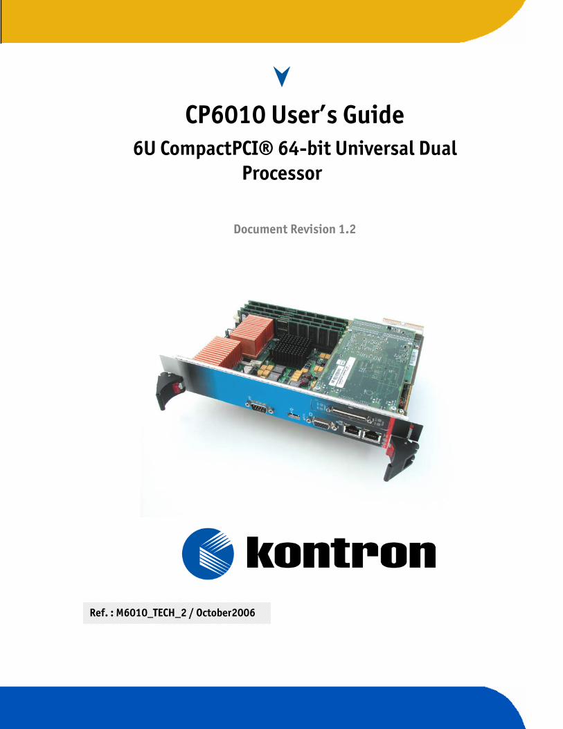
CP6010 User’s Guide 6U CompactPCI® 64-bit Universal Dual
Processor
Document Revision 1.2
Ref. : M6010_TECH_2 / October2006

i CP6010 User’s Guide
Customer Service Contact Information: Kontron Canada, Inc. 616 Curé-Boivin Boisbriand, Québec, Canada J7G 2A7 Tel: (450) 437-5682 (800) 354-4223 Fax: (450) 437-8053 E-mail: [email protected] Visit our site at: www.kontron.com © 2006 Kontron, an International Corporation. All rights reserved. The information in this user’s guide is provided for reference only. Kontron does not assume any liability arising out of the application or use of the information or products described herein. This user’s guide may contain or reference information and products protected by copyrights or patents and does not convey any license under the patent rights of Kontron, nor the rights of others. Kontron is a registered trademark of Kontron. All trademarks, registered trademarks, and trade names used in this user’s guide are the property of their respective owners. All rights reserved. Printed in Canada. This user’s guide contains information proprietary to Kontron. Customers may reprint and use this user’s guide in other publications. Customers may alter this user’s guide and publish it only after they remove the Kontron name, cover, and logo. Kontron reserves the right to make changes without notice in product or component design as warranted by evolution in user needs or progress in engineering or manufacturing technology. Changes that affect the operation of the unit will be documented in the next revision of this user’s guide.

i CP6010 User’s Guide
Contents
Customer Service Safety instructions
Before You Begin ............................................................................................ vi When Working Inside a Computer ...................................................................... vii Preventing Electrostatic Discharge ................................................................... viii Working with Batteries..................................................................................... ix
Preface How to Use This Guide..................................................................................... xii Customer Comments...................................................................................... xiii Advisory Conventions .................................................................................... xiii Unpacking................................................................................................... xiv Powering Up the System................................................................................. xiv Adapter Cables ............................................................................................. xiv Storing Boards .............................................................................................. xv Regulatory Compliance Statements ................................................................... xv Limitted Warranty ......................................................................................... xvi
1. Product Description
1.1 Product Overview ..................................................................................1-1 1.2 What’s Included....................................................................................1-1 1.3 Board Specifications..............................................................................1-2 1.4 Compact PCI Compliance.........................................................................1-5 1.5 Hot-Swap Capability ..............................................................................1-6 1.6 Interfacing with the Environment.............................................................1-9 1.7 Compatibility with Kontron Products....................................................... 1-12
2. On-board Features
2.1 Block Diagram ......................................................................................2-1 2.2 System Core .........................................................................................2-2 2.3 CSB5 South Bridge ................................................................................2-5 2.4 Super I/O PC87471 ................................................................................2-9 2.5 Ethernet Interfaces ............................................................................. 2-12 2.6 System Management Features................................................................ 2-14 2.7 Video Interface................................................................................... 2-16 2.8 CPCI Features ..................................................................................... 2-17 2.9 IPMI ................................................................................................. 2-19 2.10 Debugging Features............................................................................. 2-23 2.11 Miscellaneous Features ........................................................................ 2-25

ii CP6010 User’s Guide
3. Installing the Board 3.1 Setting Jumpers ...................................................................................3-1 3.2 Processor ............................................................................................3-3 3.3 Memory...............................................................................................3-3 3.4 On-board Interconnectivity.....................................................................3-5 3.5 Backup Battery .....................................................................................3-7 3.5 Backup Battery .....................................................................................3-7 3.6 Board Hot Swap and Installation ..............................................................3-8
4. Building a CPCI System
4.1 Building a CPCI System...........................................................................4-1 4.2 CPCI I/O Signals....................................................................................4-6
5. Software Setup
5.1 PHOENIX BIOS Setup Program..................................................................5-1 5.2 Installing Drivers ................................................................................ 5-25 5.3 Console Redirection (VT100 Mode) ......................................................... 5-26

iii CP6010 User’s Guide
A. MEMORY & I/O MAPS ........................................ A-1
A.1 Memory Mapping...................................................................................................... A-1 A.2 I/O Mapping............................................................................................................ A-2
B. Interrupt Lines ............................................... B-1
B.1 IRQ Lines ................................................................................................................ B-1 B.2 PCI Serial Interrupts ................................................................................................. B-1
C. Kontron Extension Registers.............................. C-1
C.1 FPGA/CPLD Registers Definition .................................................................................. C-1 C.2 Overview................................................................................................................. C-2 C.3 0190h: COM2 RS232/422/485 Buffer Control (FPGA)....................................................... C-3 C.4 0191h: Reset history (FPGA) ....................................................................................... C-3 C.5 0192h: Bracket Switch, Blue LED, Lock and History (FPGA & CPLD) ..................................... C-4 C.6 0193h: ID Chip and I2C Link (FPGA) ............................................................................. C-4 C.7 0196h: Watchdog Control (FPGA) ................................................................................ C-5 C.8 0197h: NMI Enables and Sources (FPGA) ....................................................................... C-5 C.9 019Bh: Backplane Information (CPLD) ......................................................................... C-5 C.10 019Ch: BMC Control (CPLD) ........................................................................................ C-6 C.11 019Dh: PCI Status Register (CPLD) ............................................................................... C-6 C.12 01A0h: Interrupt number (FPGA)................................................................................. C-7 C.13 01A1h: Interrupt enable (FPGA) .................................................................................. C-7 C.14 01A2h: PCI Interrupt status (FPGA).............................................................................. C-7 C.15 01A3h: JTAG Port (FPGA) ........................................................................................... C-8 C.16 01A8h: I2C Address (FPGA)......................................................................................... C-8 C.17 01A9h: I2C transmit (FPGA)........................................................................................ C-8 C.18 01AAh: I2C receive (FPGA) ......................................................................................... C-8 C.19 01ABh: I2C flags (FPGA) ............................................................................................ C-9
D. Connector Pinouts ........................................... D-1
D.1 Connectors and Headers Summary ............................................................................... D-1 D.2 CPCI Bus (J1)........................................................................................................... D-2 D.3 CPCI Bus (J2)........................................................................................................... D-3 D.4 CPCI Bus (J3)........................................................................................................... D-4 D.5 CPCI Bus ( PIM ) (J4) ................................................................................................. D-5 D.6 CPCI Bus ( SCSI) (J4)................................................................................................. D-6 D.7 CPCI Bus (J5)........................................................................................................... D-7 D.8 Serial Port 0 - RS-232 (J6) ......................................................................................... D-8 D.9 USB2 (located on faceplate) (J7) ................................................................................ D-8 D.10 CRT VGA Interface (J8) .............................................................................................. D-8 D.11 Ethernet LAN 2 and LAN 1 (J9, J10) ............................................................................. D-8 D.12 Hot Swap Switch (J20) .............................................................................................. D-8 D.13 Power (J22) ............................................................................................................ D-9 D.14 IDE MEZZANINE (J23)................................................................................................ D-9 D.15 Reset Switch (SW1)................................................................................................. D-10 D.16 CMOS Battery Backup Connector (BT1)........................................................................ D-10 D.17 CompactFlash™ (J3 on mezzanine) ............................................................................ D-10 D.18 JN1 – PMC ( JN1).................................................................................................... D-11

iv CP6010 User’s Guide
D.19 JN2 – PMC (JN2) .................................................................................................... D-12 D.20 JN3 – PMC (JN3) .................................................................................................... D-13 D.21 JN4 – PIM (JN4) ..................................................................................................... D-14
E. BIOS Setup Error Codes..................................... E-1
E.1 POST Beep............................................................................................................... E-1 E.2 POST Messages......................................................................................................... E-6 E.3 Error Messages......................................................................................................... E-7
F. BIOS Update & Emergency Procedure ...................F-1
F.1 BIOS UPDATE PROCEDURES ..........................................................................................F-1 F.2 EMERGENCY PROCEDURES ............................................................................................F-1
G. Getting Help .................................................. G-1

v CP6010 User’s Guide
Safety Instructions Contents
Before You Begin ................................................... vi When Working Inside a Computer ............................. vii Preventing Electrostatic Discharge .......................... viii
Working with Batteries.......................................... ix
vi CP6010 User’s Guide
Before You Begin Before handling the board, read the instructions and safety guidelines on the following pages to prevent damage to the product and to ensure your own personal safety. Refer to the “Advisories” section in the Preface for advisory conventions used in this user’s guide, including the distinction between Warnings, Cautions, Important Notes, and Notes.
♦ Always use caution when handling/operating the computer. Only qualified, experienced, authorized electronics service personnel should access the interior of the computer. The power supplies produce high voltages and energy hazards, which can cause bodily harm.
♦ Use extreme caution when installing or removing components. Refer to the installation instructions in this user’s guide for precautions and procedures. If you have any questions, please contact Kontron Post-Sales Technical Support.
WARNING
High voltages are present inside the chassis when the unit’s power cord is plugged into an electrical outlet. Turn off system power, turn off the power supply, and then disconnect the power cord from its source before removing the chassis cover. Turning off the system power switch does not remove power to components.
WARNING
This product may contain CLASS 1 LASER PRODUCT

vii CP6010 User’s Guide
When Working Inside a Computer Before taking covers off a computer, perform the following steps:
♦ Turn off the computer and any peripherals.
♦ Disconnect the computer and peripherals from power sources or subsystems to prevent electric shock or system board damage. This does not apply to when hot-swapping parts.
♦ Follow the guidelines provided in “Preventing Electrostatic Discharge“ on the following page.
♦ Disconnect telephone or telecommunications lines from the computer.
In addition, take note of these safety guidelines when appropriate:
♦ To help avoid possible damage to system boards, wait five seconds after turning off the computer before removing a component, removing a system board, or disconnecting a peripheral device from the computer.
♦ When you disconnect a cable, pull on its connector or on its strain-relief loop, not on the cable itself. Some cables have a connector with locking tabs. If you are disconnecting this type of cable, press in on the locking tabs before disconnecting the cable. As you pull connectors apart, keep them evenly aligned to avoid bending any connector pins. Also, before connecting a cable, make sue both connectors are correctly oriented and aligned.
CAUTION
Do not attempt to service the system yourself, except as explained in this user’s guide. Follow installation and troubleshooting instructions closely.

viii CP6010 User’s Guide
Preventing Electrostatic Discharge Static electricity can harm system boards. Perform service at an ESD workstation and follow proper ESD procedure to reduce the risk of damage to components. Kontron strongly encourages you to follow proper ESD procedure, which can include wrist straps and smocks, when servicing equipment. Take the following steps to prevent damage from electrostatic discharge (ESD):
♦ When unpacking a static-sensitive component from its shipping carton, do not remove the component’s antistatic packing material until you are ready to install the component in a computer. Just before unwrapping the antistatic packaging, be sure you are at an ESD workstation or grounded. This will discharge any static electricity that may have built up in your body.
♦ When transporting a sensitive component, first place it in an antistatic container or packaging.
♦ Handle all sensitive components at an ESD workstation. If possible, use antistatic floor pads and workbench pads.
♦ Handle components and boards with care. Don’t touch the components or contacts on a board. Hold a board by its edges or by its metal mounting bracket.
♦ Do not handle or store system boards near strong electrostatic, electromagnetic, magnetic, or radioactive fields.

ix CP6010 User’s Guide
Working with Batteries
Care and Handling Precautions for Lithium Batteries Your computer board has a standard, non-rechargeable lithium battery. To preserve the battery’s lifetime, the battery enable jumper has been removed for shipping.
♦ Do not short circuit
♦ Do not heat or incinerate
♦ Do not charge
♦ Do not deform or disassemble
♦ Do not apply solder directly
♦ Do not mix different types or partially used batteries together
♦ Always observe proper polarities

x CP6010 User’s Guide
Replacing Lithium Batteries Exercise caution while replacing lithium batteries!
WARNING
Danger of explosion if battery is incorrectly replaced. Replace only with the same or equivalent type recommended by the manufacturer. Dispose of used batteries, following manufacturer’s instructions.
ATTENTION
Il y a danger d’explosion s’il y a remplacement incorrect de la batterie. Remplacer uniquement avec une batterie du même type ou d’un type équivalent recommandé par le constructeur. Mettre au rebut les batteries usagées conformément aux instructions du fabriquant.
ACHTUNG
Explosionsgefahr bei falschem Batteriewechsel. Verwenden Sie nur die empfohlenen Batterietypen des Herstellers. Entsorgen Sie die verbrauchten Batterien laut Gebrauchsanweisung des Herstellers.
ATENCION
Puede explotar si la pila no este bien reemplazada. Solo reemplazca la pila con tipas equivalentes segun las instrucciones del manifacturo. Vote las pilas usads segun las instrucciones del manifacturo.

xi CP6010 User’s Guide
Preface Contents
How to Use This Guide............................................ xii Customer Comments............................................. xiii Advisory Conventions ........................................... xiii Unpacking.......................................................... xiv Powering Up the System........................................ xiv Adapter Cables .................................................... xiv Storing Boards ..................................................... xv Regulatory Compliance Statements .......................... xv Limitted Warranty ................................................ xvi

xii CP6010 User’s Guide
How to Use This Guide This user’s guide provides step-by-step instructions for installation and serves as a reference for operation, troubleshooting, and upgrades. You can find the latest release of this User’s Guide at: ftp://ftp.kontron.ca/support/ For the circuits, descriptions and tables indicated, Kontron assumes no responsibility as far as patents or other rights of third parties are concerned. The following is a summary of chapter contents:
♦ Chapter 1, Product Description
♦ Chapter 2, On-board Features
♦ Chapter 3, Installing the board
♦ Chapter 4, Building a CPCI System
♦ Chapter 5, Software Setup
♦ Appendix A, Memory & I/O Maps
♦ Appendix B, Interrupt Lines
♦ Appendix C, Kontron Extension Registers
♦ Appendix D, Board Diagrams
♦ Appendix E, Connector Pinouts
♦ Appendix F, BIOS Setup Error Codes
♦ Appendix G, BIOS Update & Emergency Procedure
♦ Appendix H, Getting Help
xiii CP6010 User’s Guide
Customer Comments If you have any difficulties using this user’s guide, discover an error, or just want to provide some feedback, please send us a message at [email protected]. Detail any errors you find. We will correct the errors or problems as soon as possible and post the revised user’s guide in our online Support Library. Thank you.
Advisory Conventions Seven types of advisories are used throughout the user guides to provide helpful information or to alert you to the potential for hardware damage or personal injury. They are Note, Signal Paths, Related Jumpers, BIOS Settings, Software Usage, Cautions, and Warnings. The following is an example of each type of advisory. Use caution when servicing electrical components.
Note: Indicates information that is important for you to know.
Signal Paths: Indicates the places where you can find the signal on the board.
Related Jumpers: Indicates the jumpers that are related to this sections.
BIOS Settings: Indicates where you can set this option in the BIOS.
Software Usage: Indicates how you can access this feature through software.
CAUTION
Indicates potential damage to hardware and tells you how to avoid the problem.
WARNING
Indicates the potential for bodily harm and tells you how to avoid the problem.
Disclaimer: We have tried to identify all situations that may pose a warning or a caution condition in this user’s guide. However, Kontron does not claim to have covered all situations that might require the use of a Caution or a Warning.

xiv CP6010 User’s Guide
Unpacking
Follow these recommendations while unpacking:
♦ Remove all items from the box. If any items listed on the purchase order are missing, notify Kontron customer service immediately.
♦ Inspect the product for damage. If there is damage, notify Kontron customer service immediately.
♦ Save the box and packing material for possible future shipment.
Powering Up the System Before any installation or setup, ensure that the board is unplugged from power sources or subsystems. If you encounter a problem, verify the following items:
♦ Make sure that all connectors are properly connected.
♦ Verify your boot devices.
♦ If the system does not start properly, try booting with only the video monitor connected to the board and without any other I/O peripherals attached, including Compact PCI or PMC adapters.
If you still cannot start your system, please refer to the Emergency Procedure in the Appendix Section of this User’s Guide. If you are still not able to get your board running, contact our Technical Support for assistance. Make sure your system provides the minimum DC voltages required at the board’s slot, especially if cables carry DC power.

xv CP6010 User’s Guide
Adapter Cables Because adapter cables come from various manufacturers, pinouts can differ. The direct crimp design offered by Kontron allows the simplest cable assembly. All cables are available from Kontron.
Storing Boards Electronic boards are sensitive devices. Do not handle or store device near strong electrostatic, electromagnetic, magnetic, or radioactive fields.
Regulatory Compliance Statements This section provides the FCC compliance statement for Class B devices and describes how to keep the system CE compliant.
FCC Compliance Statement for Class B Devices This equipment has been tested and found to comply with the limits for a Class B digital device, pursuant to Part 15 of the FCC Rules. These limits are designed to provide reasonable protection against harmful interference in a residential installation. This equipment generated, uses and can radiate radio frequency energy and, if not installed and used in accordance with the instructions may cause harmful interference to radio communications. However, there is no guarantee that interference will not occur in a particular installation If this equipment does cause harmful interference to radio or television reception, which can be determined by turning the equipment off and on, the user is encourage to try to correct the interference by one or more of the following measures:
• Reorient or relocate the receiving antenna. • Increase the separation between the equipment and receiver.
• Connect the equipment into an outlet on a circuit different from that to which the
receiver is connected.
• Consult the dealer or an experience radio/TV technician for help.
WARNING
This is a Class B product. If not installed in a properly shielded enclosure and used in accordance with this User’s Guide, this product may cause radio interference in which case users may need to take additional measures at their own expense. Changes or modifications not expressly approved by the party responsible for compliance could void the user’s authority to operate this product.

xvi CP6010 User’s Guide
UL Certification This product bears the combined UL Recognized Component Mark for Canada and U.S. It indicates investigations to the UL Standard for Safety of Information Technology Equipment, Including Electrical Business
Equipment. It is designated to be used in end-product equipment where the acceptability of the combination is determined by Underwriters Laboratories Inc.
CE Certification The product(s) described in this user’s guide complies with all applicable European Union (CE) directives if it has a CE marking. For computer systems to remain CE
compliant, only CE-compliant parts may be used. Maintaining CE compliance also requires proper cable and cabling techniques. Although Kontron offers accessories, the customer must ensure that these products are installed with proper shielding to maintain CE compliance. Kontron does not offer engineering services for designing cabling systems. In addition, Kontron will not retest or recertify systems or components that have been reconfigured by customers.
LIMITED WARRANTY Kontron Canada, Inc, (“The seller”) warrants its boards to be free from defects in material and workmanship for a period of two (2) years commencing on the date of shipment. The liability of the seller shall be limited to replacing or repairing, at the seller’s option, any defective units. Equipment or parts, which have been subject to abuse, misuse, accident, alteration, neglect, or unauthorized repair are not covered by this warranty. This warranty is in lieu of all other warranties expressed or implied.

1-0 CP6010 User’s Guide
1. Product Description Contents
1.1 Product Overview .........................................1-1 1.2 What’s Included...........................................1-1 1.3 Board Specifications.....................................1-2 1.4 Compact PCI Compliance................................1-5 1.5 Hot-Swap Capability .....................................1-6 1.6 Interfacing with the Environment.................. 1-69 1.7 Compatibility with Kontron Products................1-9

1-1 CP6010 User’s Guide
1.1 Product Overview Kontron’s CP6010 can accommodate the endless demands for increased bandwidth among mission-critical voice messaging, Computer Telephony Integration (CTI) and Internet/Intranet server applications. This board is a state-of-the-art Dual CPU High Performance Serverworks-based CompactPCI 6U/8HP) system or peripheral processor. It complements Kontron’s current family of 6U CompactPCI™ processor boards offering by addressing the very high performance needs of the data / telecommunication and CTI server. The CP6010 packs new power onto a single board computer (SBC) by incorporating two Intel PIV Xeon processors at speeds of 1.6GHz, 2.0GHz, 2.4GHz and 2.8GHz, a front side bus of 400/533MHz and up to 8GB of DDR system memory. Its performance is further enhanced by using one 64-bit/133MHz PCI-X bus, which effectively increase by four the PCI bandwidths over previous products. The CP6010 is fully hot swappable and meets all the requirement needed to build high availability CPCI systems. In addition, the CP6010 can communicate at 4Gb/s over two full duplex gigabit Ethernet links with other processor boards using a CompactPCI 2.16 backplane (XL-PSB/VHDS Platform) for high density and high reliability clustering applications. The CP6010 offers a natural growth path to high performance, high availability as well as hot swappable and scalable multiprocessing technology.
1.2 What’s Included This board is shipped with the following items:
• One CP6010 board
• One quick reference sheet
• Cables that have been ordered
If any item is missing or damaged, contact the supplier.

1-2 CP6010 User’s Guide
1.3 Board Specifications FEATURES DESCRIPTION
Supported Microprocessors
• Dual Intel Low Voltage XEON® Processor at 400/533MHz front side bus (FSB)
• Supports Hyper-Threading
• NetBurst™ Architecture
Cache Memory • 512K L2 on-die cache
• 12KB/8KB Instruction/Data Level 1
Chipset
• ServerWorks GC-LE server chipset with CSB5 South Bridge
• ServerWorks CIOB-X2 for dual PCI-X 133MHz interface
• National PC87417 super I/O
Bus Interface
• Front side bus at 400/533 MHz, 64-bit data, 36-bit address
• Memory bus at 200/266 MHz, 144-bit data (2 channel)
• One on-board 64-bit/133MHz PCI-X bus
• One on-board 64-bit/66MHz PCI bus
• CPCI PCI 64-bit/66MHz with universal bridge
• One on-board 32-bit/33MHz bus for video interface
System Memory
• Up to 8GB on 4 x 184-pin latching DIMM sockets, 64/72-bit
• Two DDR channels 72-bit/133MHz for Interleave operation
• PC-1600/PC-2100 DDR, registered SDRAM non-ECC/ECC mode (ECC error correction up to a nibble, error detection for more than a nibble); all eight GB cacheable
Flash Memory • 512KB for BIOS field upgrade on X-BUS
• 32KB user serial EEPROM
1-3 CP6010 User’s Guide
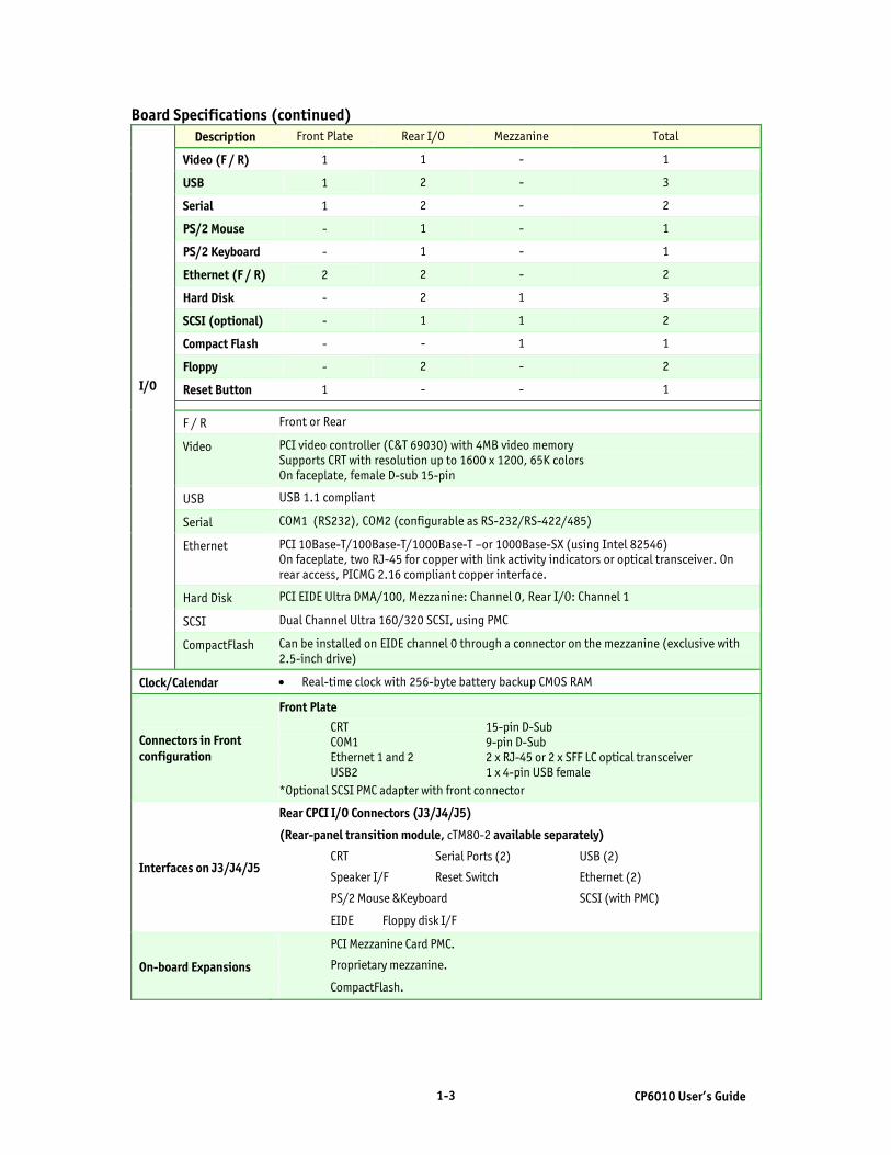
Board Specifications (continued) Description Front Plate Rear I/O Mezzanine Total
Video (F / R) 1 1 - 1
USB 1 2 - 3
Serial 1 2 - 2
PS/2 Mouse - 1 - 1
PS/2 Keyboard - 1 - 1
Ethernet (F / R) 2 2 - 2
Hard Disk - 2 1 3
SCSI (optional) - 1 1 2
Compact Flash - - 1 1
Floppy - 2 - 2
Reset Button 1 - - 1
F / R Front or Rear
Video PCI video controller (C&T 69030) with 4MB video memory Supports CRT with resolution up to 1600 x 1200, 65K colors On faceplate, female D-sub 15-pin
USB USB 1.1 compliant
Serial COM1 (RS232), COM2 (configurable as RS-232/RS-422/485)
Ethernet PCI 10Base-T/100Base-T/1000Base-T –or 1000Base-SX (using Intel 82546) On faceplate, two RJ-45 for copper with link activity indicators or optical transceiver. On rear access, PICMG 2.16 compliant copper interface.
Hard Disk PCI EIDE Ultra DMA/100, Mezzanine: Channel 0, Rear I/O: Channel 1
SCSI Dual Channel Ultra 160/320 SCSI, using PMC
I/O
CompactFlash Can be installed on EIDE channel 0 through a connector on the mezzanine (exclusive with 2.5-inch drive)
Clock/Calendar • Real-time clock with 256-byte battery backup CMOS RAM
Connectors in Front configuration
Front Plate CRT 15-pin D-Sub COM1 9-pin D-Sub Ethernet 1 and 2 2 x RJ-45 or 2 x SFF LC optical transceiver USB2 1 x 4-pin USB female *Optional SCSI PMC adapter with front connector
Interfaces on J3/J4/J5
Rear CPCI I/O Connectors (J3/J4/J5)
(Rear-panel transition module, cTM80-2 available separately)
CRT Serial Ports (2) USB (2)
Speaker I/F Reset Switch Ethernet (2)
PS/2 Mouse &Keyboard SCSI (with PMC)
EIDE Floppy disk I/F
On-board Expansions
PCI Mezzanine Card PMC.
Proprietary mezzanine.
CompactFlash.
1-4 CP6010 User’s Guide
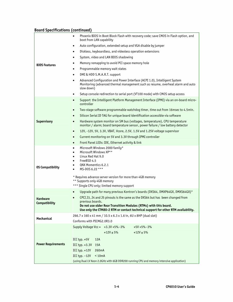
Board Specifications (continued)
BIOS Features
• Phoenix BIOS in Boot Block Flash with recovery code; save CMOS in Flash option, and boot from LAN capability
• Auto configuration, extended setup and VGA disable by jumper
• Diskless, keyboardless, and videoless operation extensions
• System, video and LAN BIOS shadowing
• Memory remapping to avoid PCI space memory hole
• Programmable memory wait states
• DMI & HDD S.M.A.R.T. support
• Advanced Configuration and Power Interface (ACPI 1.0), Intelligent System Monitoring (advanced thermal management such as resume, overheat alarm and auto slow down)
• Setup console redirection to serial port (VT100 mode) with CMOS setup access
Supervisory
• Support the Intelligent Platform Management Interface (IPMI) via an on-board micro-controller
• Two-stage software programmable watchdog timer, time out from 16msec to 4.5min.
• Silicon Serial ID TAG for unique board identification accessible via software
• Hardware system monitor on SM bus (voltages, temperature), CPU temperature monitor / alarm; board temperature sensor, power failure / low battery detector
• 12V, -12V, 5V, 3.3V, VBAT, Vcore, 2.5V, 1.5V and 1.25V voltage supervisor
• Current monitoring on 5V and 3.3V through IPMI controller
• Front Panel LEDs: IDE, Ethernet activity & link
OS Compatibility
• Microsoft Windows 2000 family* • Microsoft Windows XP** • Linux Red Hat 9.0 • FreeBSD 4.5 • QNX Momentics 6.2.1 • MS-DOS 6.22 *** * Requires advance server version for more than 4GB memory ** Supports only 4GB memory *** Single CPU only; limited memory support
Hardware Compatibility
• Upgrade path for many previous Kontron’s boards (DXS64, DMXP64GX, DMXS64GX)*
• CPCI J3, J4 and J5 pinouts is the same as the DXS64 but has been changed from previous boards. Do not use older Rear Transition Modules (RTMs) with this board. Use only the CTM80-2 RTM or contact technical support for other RTM availability.
Mechanical 266.7 x 160 x 41 mm / 10.5 x 6.3 x 1.6 in, 6U x 8HP (dual slot)
Conforms with PICMG2.0R3.0
Power Requirements
Supply Voltage Vcc = +3.3V +5% -3% +5V +5% -3%
+12V ± 5% +12V ± 5%
ICC typ. +5V 12A
ICC typ. +3.3V 15A
ICC typ. +12V 260mA
ICC typ. –12V < 10mA
(using Dual LV Xeon 2.0GHz with 6GB DDR200 running CPU and memory intensive application)
1-5 CP6010 User’s Guide
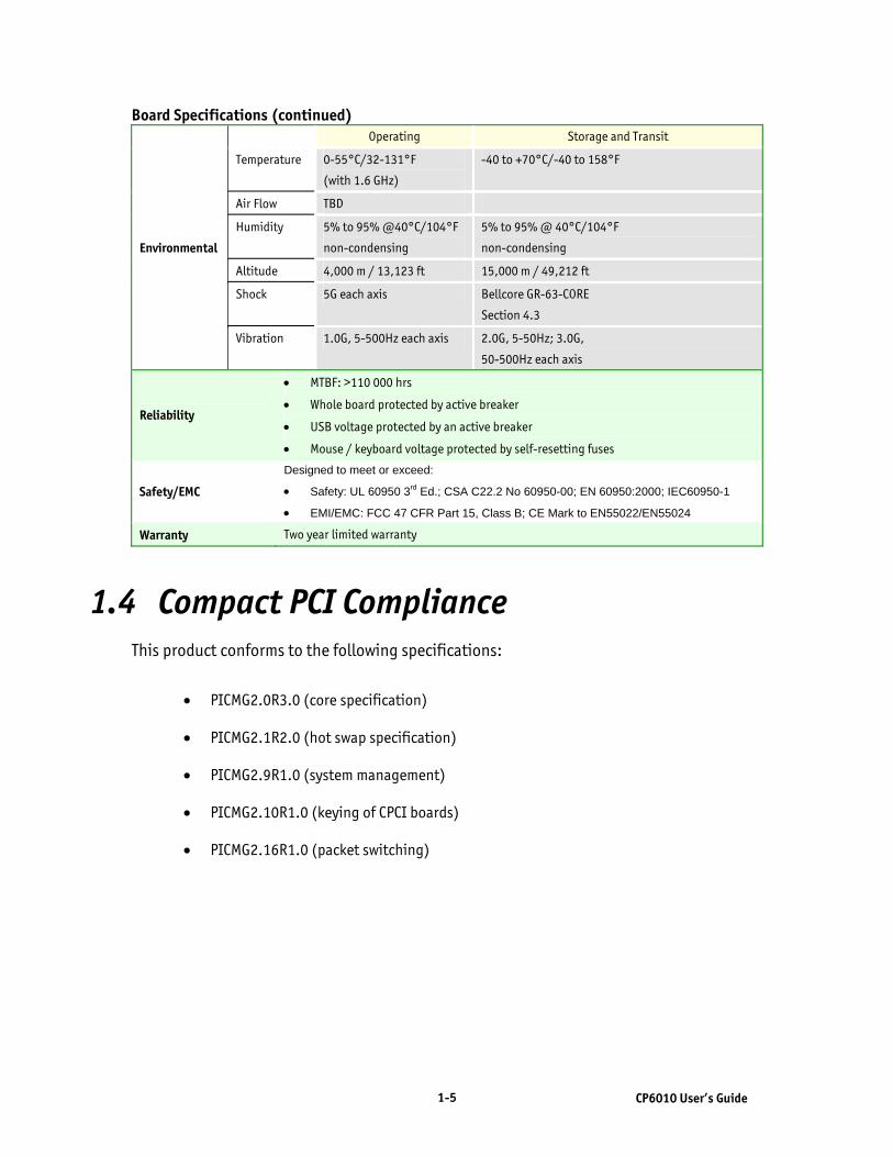
Board Specifications (continued) Operating Storage and Transit
Temperature 0-55°C/32-131°F
(with 1.6 GHz)
-40 to +70°C/-40 to 158°F
Air Flow TBD
Humidity 5% to 95% @40°C/104°F
non-condensing
5% to 95% @ 40°C/104°F
non-condensing
Altitude 4,000 m / 13,123 ft 15,000 m / 49,212 ft
Shock 5G each axis Bellcore GR-63-CORE
Section 4.3
Environmental
Vibration 1.0G, 5-500Hz each axis 2.0G, 5-50Hz; 3.0G,
50-500Hz each axis
Reliability
• MTBF: >110 000 hrs
• Whole board protected by active breaker
• USB voltage protected by an active breaker
• Mouse / keyboard voltage protected by self-resetting fuses
Safety/EMC
Designed to meet or exceed:
• Safety: UL 60950 3rd Ed.; CSA C22.2 No 60950-00; EN 60950:2000; IEC60950-1
• EMI/EMC: FCC 47 CFR Part 15, Class B; CE Mark to EN55022/EN55024
Warranty Two year limited warranty
1.4 Compact PCI Compliance This product conforms to the following specifications:
• PICMG2.0R3.0 (core specification)
• PICMG2.1R2.0 (hot swap specification)
• PICMG2.9R1.0 (system management)
• PICMG2.10R1.0 (keying of CPCI boards)
• PICMG2.16R1.0 (packet switching)
1-6 CP6010 User’s Guide
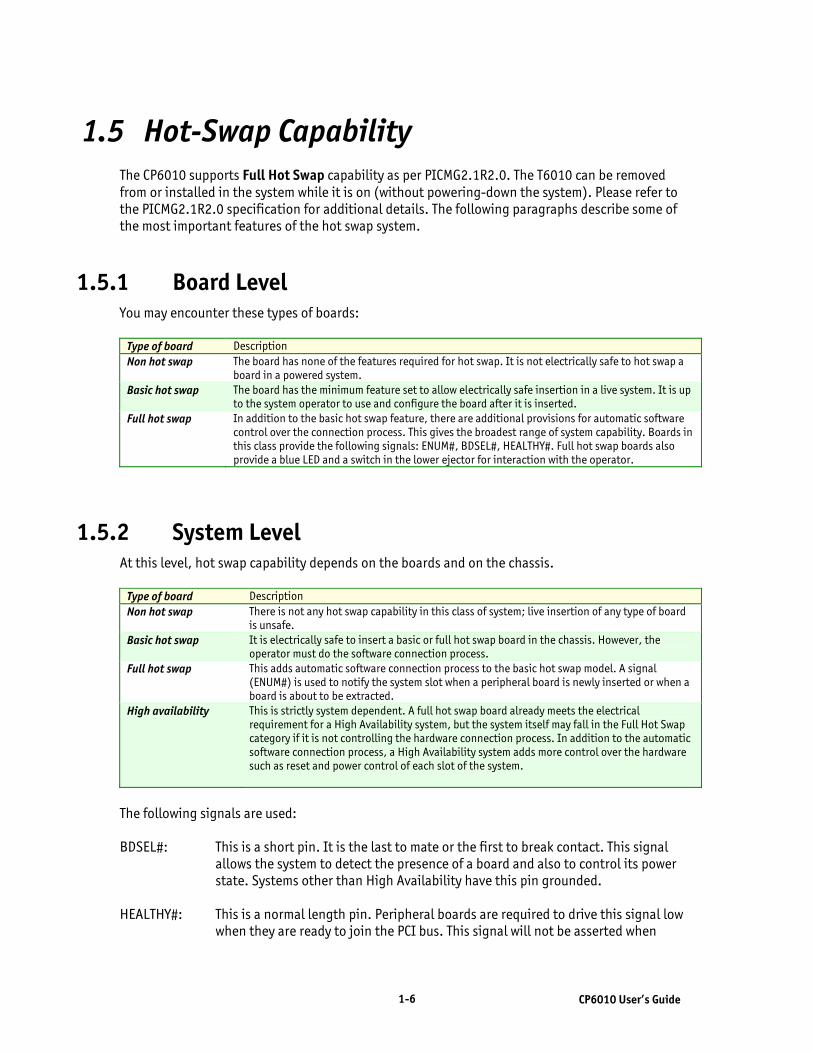
1.5 Hot-Swap Capability The CP6010 supports Full Hot Swap capability as per PICMG2.1R2.0. The T6010 can be removed from or installed in the system while it is on (without powering-down the system). Please refer to the PICMG2.1R2.0 specification for additional details. The following paragraphs describe some of the most important features of the hot swap system.
1.5.1 Board Level You may encounter these types of boards:
Type of board Description Non hot swap The board has none of the features required for hot swap. It is not electrically safe to hot swap a
board in a powered system. Basic hot swap The board has the minimum feature set to allow electrically safe insertion in a live system. It is up
to the system operator to use and configure the board after it is inserted. Full hot swap In addition to the basic hot swap feature, there are additional provisions for automatic software
control over the connection process. This gives the broadest range of system capability. Boards in this class provide the following signals: ENUM#, BDSEL#, HEALTHY#. Full hot swap boards also provide a blue LED and a switch in the lower ejector for interaction with the operator.
1.5.2 System Level At this level, hot swap capability depends on the boards and on the chassis.
Type of board Description Non hot swap There is not any hot swap capability in this class of system; live insertion of any type of board
is unsafe. Basic hot swap It is electrically safe to insert a basic or full hot swap board in the chassis. However, the
operator must do the software connection process. Full hot swap This adds automatic software connection process to the basic hot swap model. A signal
(ENUM#) is used to notify the system slot when a peripheral board is newly inserted or when a board is about to be extracted.
High availability This is strictly system dependent. A full hot swap board already meets the electrical requirement for a High Availability system, but the system itself may fall in the Full Hot Swap category if it is not controlling the hardware connection process. In addition to the automatic software connection process, a High Availability system adds more control over the hardware such as reset and power control of each slot of the system.
The following signals are used: BDSEL#: This is a short pin. It is the last to mate or the first to break contact. This signal allows the system to detect the presence of a board and also to control its power state. Systems other than High Availability have this pin grounded. HEALTHY#: This is a normal length pin. Peripheral boards are required to drive this signal low when they are ready to join the PCI bus. This signal will not be asserted when
1-7 CP6010 User’s Guide
the current operating mode of the bus is not compatible or when the back end power is not good or for any other reason.
PCIRST#: This signal resets the PCI bus when driven low. High availability can implement this signal as a radial signal from the Hot Swap Controller (HSC) to further control the electrical connection. Platforms that do this must OR the system host’s reset signal with the slot-specific signal to maintain the bused signal’s function. M66EN: On a High Availability platform compatible with R. 2.0 of PICMG2.1, the signal may be radial from the HSC. This allows the platform to accept 33MHz only peripheral boards that comply with R. 1 of the specification.
Note: Hot Swap of the system slot is not defined in the PICMG2.1R2.0 specification. It is electrically possible to hot swap the CP6010 in a system slot, but system functionality is lost and the PCI bus will float.
WARNING
It can be harmful for some PCI peripheral devices to remove system slots because the PCI bus floats. At least PCIRST# should be asserted but not all platforms detect this condition and hold the system in reset when a system board is not present. Please consult your chassis manual.
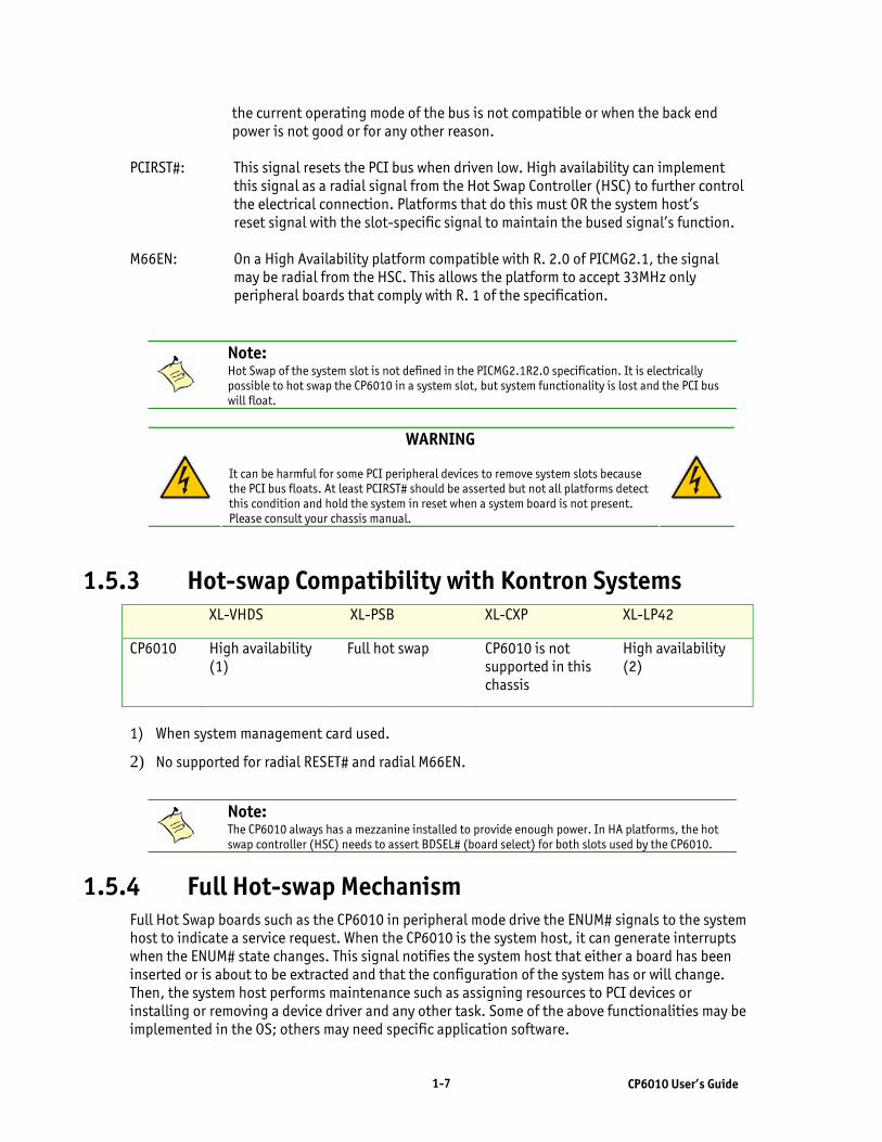
1.5.3 Hot-swap Compatibility with Kontron Systems XL-VHDS XL-PSB XL-CXP XL-LP42
CP6010 High availability (1)
Full hot swap CP6010 is not supported in this chassis
High availability (2)
1) When system management card used.
2) No supported for radial RESET# and radial M66EN.
Note: The CP6010 always has a mezzanine installed to provide enough power. In HA platforms, the hot swap controller (HSC) needs to assert BDSEL# (board select) for both slots used by the CP6010.
1.5.4 Full Hot-swap Mechanism Full Hot Swap boards such as the CP6010 in peripheral mode drive the ENUM# signals to the system host to indicate a service request. When the CP6010 is the system host, it can generate interrupts when the ENUM# state changes. This signal notifies the system host that either a board has been inserted or is about to be extracted and that the configuration of the system has or will change. Then, the system host performs maintenance such as assigning resources to PCI devices or installing or removing a device driver and any other task. Some of the above functionalities may be implemented in the OS; others may need specific application software.

1-8 CP6010 User’s Guide
The Hot Swap Switch is in the lower ejector. It allows the operator to inform the system about the intention to extract the board. A blue LED, located on the board’s faceplate, illuminates when it is safe to extract the board. This LED indicates that the system software has been placed in a state for orderly extraction of a board. The hardware connection layer provides protection only for the hardware during insertions and extractions. This method allows the operator to insert or to extract boards without reconfiguring the system with the console.
Note: To detect handle switch activity and to signal board status with the blue LED, the host must have a proper hot swap driver.
The end user must know that adding a PCI device to a live system requires allocating PCI resources. The OS does not do this; the hot swap driver does. However, many configurations can be done only from the BIOS. Consult Kontron’s technical support if you need additional information.
WARNING
All actions are initiated by the operator and must be performed in the correct sequence for proper system operation.
Full Hot Swap boards present the following resources to software executing on the system host (nominally implementing the Hot-Plug Service and Hot-Plug System Driver).
An ENUM# signal, which is an open collector (open drain) bused signal; it signals a change in the board status.
A switch actuated with the lower ejector handle indicates the beginning of the extraction process or the end of the insertion process.
A LED indicates the status of the software connection process.
A set of four control and status bits (hot swap register in PCI configuration space) on each board allows the system host’s software to determine the source of the ENUM# signal and control the LED.
1.5.5 High Availability Mechanism When using a High Availability system such as XL-VHDS and XL-LP42, the system has more control over the hardware connection process compared to the full, hot-swap model. When a board is inserted in the system, the Hot Swap Controller (HSC) detects the insertion before powering up the newly inserted board. When the HSC is ready to power up a card, it asserts BDSEL# and monitors the HEALTHY# signal for that card. This flexibility gives the possibility to the operator, for example, to cycle the power state of a problematic I/O board or to reset only a particular slot. Please refer to your system manual for more details on how to use the High Availability feature of the system.
In addition to the resources a board present on a Full Hot Swap system, the following ones are usable on HA systems:
• A BDSEL# signal controls the power state of the board
• A HEALTHY# signal indicates the healthiness of the board

1-9 CP6010 User’s Guide
1.5.5.1 Bus-less Operation When the on-board bridge is disabled, the CP6010 is considered bus less. In such cases, the SBC can be hot swapped in a CPCI bus but will not try to participate on the bus. Then, BDSEL# and HEALTHY# preserve their functionality but PCIRST# is ignored. The blue LED mechanism is disabled because the on-board bridge and system host cannot handle it. However, it is possible to read the handle switch and control the blue LED through register 0x192.
Note: When the bridge is disabled (stand-alone operation), the user can read the hot-swap switch and drive blue LED by using register 0x192.
1.6 Interfacing with the Environment
1.6.1 CPCI The CP6010 system/peripheral processor board is provided for rack-mounted systems to offer the highest modularity. Through the J1/J2 segment, the board can drive up to seven external CompactPCI slots, supporting individual REQ/GNT arbitration pair signals and the clock. The CP6010 supports all PCI modes for operation up to 66MHz, giving a theoretical throughput of 512MB/s.
Possible PCI modes of the CP6010 with Kontron systems:
XL-VHDS (1) XL-PSB XL-CXP XL-LP42
CP6010 PCI-33
PCI-66
PCI-33
PCI-33 PCI-33
PCI-66
1) Using a five-slot backplane.
1.6.2 RTM All I/Os can be accessed through a rear transition module (RTM). RTMs use proprietary pinouts in J3/J4/J5 to bring out all I/Os of the SBC. Only use Kontron’s RTM with the CP6010. The cTM-80 is compatible with the RTM . RTMs are not designed to be hot swapped when a front board is present. Make sure that either the system is shut off or that the front board of the RTM is unpowered before removing or installing a RTM.
Note : A. In front I/O configurations, the following I/O signals are available on the faceplate: SVGA,
Serial Port COM1, USB Port 2, Ethernet 1 and 2. All other I/Os connect to J3, J4, and J5.
B. In Rear I/O configurations, all I/O signals connect to J3, J4, and J5
1-10 CP6010 User’s Guide
1.6.3 Mezzanine The mezzanine is a hardware interface used to increase I/O connectivity of the CP6010 while respecting the dual slot 6U form-factor restrictions. It is built around three sets of connectors: • Mezzanine connector handling IDE signals, additional PCI slots and arbitration signals, 5V
power.
• Mezzanine connector (the four baseboard PMC connector) that handles a complete PCI signal set, including the REQ/GNT arbitration signal pair.
• A two-pin power connector to bring additional 3.3V on the baseboard.
These connectors represent an open door for future development of expansion and I/O mezzanine cards. The following I/O’s are available on the T6507 mezzanine:
• PMC connector supporting PCIX up to 133MHz, 64 bits PMC with PIM interface.
Note: If you encounter problem with the GB Ethernet LAN adapter, set the PMC bus to PCI-66. There is no performance degradation.
• CompactFlash connector supporting Type 1 and 2 modules.
• IDE connector for 2.5-inch hard disk (exclusive with PMC, and CompactFlash).
See Kontron’s mezzanine offering for additional I/O capabilities.
1.6.3.1 CompactFlash/Hard-disk Feature Using a mezzanine, the CP6010 board also supports standard CompactFlash disk through a CompactFlash module or a 2.5-inch hard drive.
1.6.3.2 Provides Additional Power The CP6010 is a high-performance CPU board that needs more current than what one CPCI slot can provide. To overcome this, part of the required current comes from the mezzanine’s J1 connector.
1.6.3.3 PMC Expansion The mezzanine increases the I/O capability of the CP6010 by providing a PMC slot. Up to 133MHZ/64-bits are supported for up to 1GB of I/O bandwidth.
Note: The CP6010 requires a mezzanine for proper operation. Without a mezzanine, the board remains without power, and the blue LED will stay on. The CP6010 requires a slot (either system), peripheral or bus-less for the mezzanine. Many systems that have a system slot at the right of a backplane fail to meet this requirement, preventing the use of the CP6010 as a system host controller.

1-11 CP6010 User’s Guide
The capability of the CP6010 to connect with other devices is enforced by PCI Mezzanine Cards (PMC). A fully equipped CP6010 board may appear as follows:
CP6010 with SCSI Mezzanine
CP6010 with HDD Mezzanine
1-12 CP6010 User’s Guide
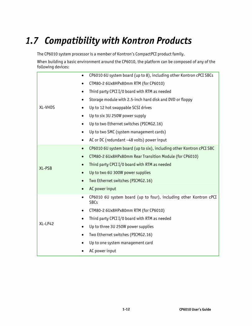
1.7 Compatibility with Kontron Products The CP6010 system processor is a member of Kontron’s CompactPCI product family.
When building a basic environment around the CP6010, the platform can be composed of any of the following devices:
XL-VHDS
• CP6010 6U system board (up to 8), including other Kontron cPCI SBCs
• CTM80-2 6Ux8HPx80mm RTM (for CP6010)
• Third party CPCI I/0 board with RTM as needed
• Storage module with 2.5-inch hard disk and DVD or floppy
• Up to 12 hot swappable SCSI drives
• Up to six 3U 250W power supply
• Up to two Ethernet switches (PICMG2.16)
• Up to two SMC (system management cards)
• AC or DC (redundant –48 volts) power input
XL-PSB
• CP6010 6U system board (up to six), including other Kontron cPCI SBC
• CTM80-2 6Ux8HPx80mm Rear Transition Module (for CP6010)
• Third party CPCI I/0 board with RTM as needed
• Up to two 6U 300W power supplies
• Two Ethernet switches (PICMG2.16)
• AC power input
XL-LP42
• CP6010 6U system board (up to four), including other Kontron cPCI SBCs
• CTM80-2 6Ux8HPx80mm RTM (for CP6010)
• Third party CPCI I/0 board with RTM as needed
• Up to three 3U 250W power supplies
• Two Ethernet switches (PICMG2.16)
• Up to one system management card
• AC power input

2-0 CP6010 User’s Guide
2. On-board Features Contents
2.1 Block Diagram ................................................. 2-1 2.2 System Core .................................................... 2-2 2.3 CSB5 South Bridge ........................................... 2-5 2.4 Super I/O PC87471 ........................................... 2-9 2.5 Ethernet Interfaces .......................................... 2-12 2.6 System Management Features............................. 2-14 2.7 Video Interface................................................ 2-16 2.8 CPCI Features .................................................. 2-17 2.9 IPMI .............................................................. 2-19 2.10 Debugging Features.......................................... 2-23 2.11 Miscellaneous Features ..................................... 2-25

2-1 CP6010 User’s Guide
2.1 Block Diagram
2-2 CP6010 User’s Guide
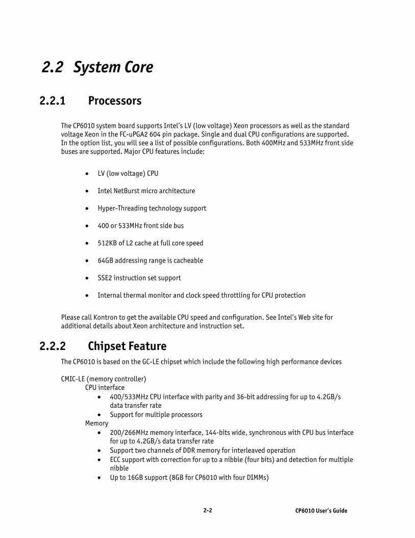
2.2 System Core
2.2.1 Processors The CP6010 system board supports Intel’s LV (low voltage) Xeon processors as well as the standard voltage Xeon in the FC-uPGA2 604 pin package. Single and dual CPU configurations are supported. In the option list, you will see a list of possible configurations. Both 400MHz and 533MHz front side buses are supported. Major CPU features include:
• LV (low voltage) CPU
• Intel NetBurst micro architecture
• Hyper-Threading technology support
• 400 or 533MHz front side bus
• 512KB of L2 cache at full core speed
• 64GB addressing range is cacheable
• SSE2 instruction set support
• Internal thermal monitor and clock speed throttling for CPU protection
Please call Kontron to get the available CPU speed and configuration. See Intel’s Web site for additional details about Xeon architecture and instruction set.
2.2.2 Chipset Feature The CP6010 is based on the GC-LE chipset which include the following high performance devices CMIC-LE (memory controller) CPU interface
• 400/533MHz CPU interface with parity and 36-bit addressing for up to 4.2GB/s data transfer rate
• Support for multiple processors Memory
• 200/266MHz memory interface, 144-bits wide, synchronous with CPU bus interface for up to 4.2GB/s data transfer rate
• Support two channels of DDR memory for interleaved operation • ECC support with correction for up to a nibble (four bits) and detection for multiple
nibble • Up to 16GB support (8GB for CP6010 with four DIMMs)

2-3 CP6010 User’s Guide
• Memory scrubbing support (chipset automatically scans memory and corrects ECC errors)
• Support 12 deep for in-order queue • Eight cache line read buffers, eight cache line write buffers • Support for read around write
IMB (Inter-Module Bus) • 800MHz IMB for 3.2GB/s transfer rate between CMIC-LE and CIOB-X2 • CRC protected IMB • Multiple IOAPIC support • Allow concurrency between IMB and CPU interface transaction
CIOB-X2 (PCI-X bus interface)
• Support 800MHz IMB • Parity protection on PCI/PCI-X • Allow concurrency between PCI/PCI-X bus and IMB • Eight deep outbound request queue for IMB to PCI/PCI-X transaction • Eight deep IMB to PCI/PCI-X memory write posting transaction • Caching of PCI to main memory transaction for each PCI bus • Peer to peer transaction support • PCIX bus error reporting
CSB5 (South bridge)
• Supports thin IMB interface for 100MB/s transfer in both directions • 32-bits/33MHz PCI bus • Provide legacy functions (8237 DMA, 8259 PIC, 8254 timer) • PCI to LPC bridge • USB 1.1 interfaces • Two ATA/100 EIDE interface
Note: Many errors can be monitored by setting the DMI event BIOS menu such as ECC errors, parity errors on all PCI/PCI-X buses, and more. See the BIOS section for details.

2-4 CP6010 User’s Guide
2.2.3 Memory Interface This product supports up to eight Gigabytes (all 8GB is cacheable) on 4 x 184-pin latching DIMM sockets. Supported memory includes PC-1600/PC-2100 DDR, 2.5V registered SDRAM, non-ECC/ECC mode. The CMIC-LE memory controller is capable of up to a nibble error correction and multiple nibble error detection via. There are two DDR channels 72-bit/133MHz for interleave operation to match the bandwidth of the CPU front side bus. The memory controller is optimized for applications that use huge amounts of memory and have the following high end feature: Memory remapping: Memory remapping allows mapping memory that is usually below 4GB at a higher address. This has the advantage of freeing a physical memory area for PCI devices below the 4GB boundary without losing physical memory to overlapping. If your OS does not support memory capacity above 4GB, disable this feature in the BIOS. Memory will be remapped above 4GB. Memory scrubbing: This feature allows the CMIC-LE to automatically correct ECC errors and write back the good data into memory without the CPU intervening. This is done in hardware. ChipKill: CMIC-LE supports ChipKill memory technology, which allows the system to function normally even with one bad DDR SDRAM device. This bad DDR SDRAM device must be an X4 device. ChipKill memory technology works by reordering the data from the DDR SDRAMs so that if a DDR SDRAM device should fail, correctable ECC errors are generated, instead of uncorrectable ECC errors. With correctable ECC errors, the system functions normally without corrupting data.

2-5 CP6010 User’s Guide
2.3 CSB5 South Bridge
2.3.1 Enhanced IDE Interface The EIDE interface is part of the CSB5 south bridge. The interface conforms to the ATA specification and supports ATA100 for 100MB/s burst transfers. The board features two channel bus master PCI EIDEs that are dedicated to primary and secondary IDE logical interfaces. The secondary channel is available only from the RTM. Each channel supports up to two IDE devices, including CD-ROMs, hard disks, CompactFlash on the primary IDE interface and offers independent timings in master/slave combination. The IDE interfaces support PIO Mode 4 transfers up to 16.6MB/sec and bus master IDE transfers up to 100MB/sec (ultra DMA/100).
Signal Paths:
The primary IDE interface is only available through the Mezzanine connector. The secondary IDE interface is only available through the CPCI I/O connector.
Related Jumpers: W1 must be removed when CompactFlash is used. W1 must be installed when 2.5-inch drive used.
BIOS Settings: Section 5.1.2.5 , Advanced Menu Selection
CAUTION
Two master devices (or two slave devices) must not be installed on the same interface at the same time.
2.3.1.1 CompactFlash Interface The board supports an IDE compatible flash disk by using a CompactFlash module. CompactFlash (C-Flash) disks are the industry-standard ATA/IDE subsystem for application, data, image, and audio storage. They have the same functionality and capabilities as intelligent disk drives but with the advantages of being very compact, rugged (typical MTBF is 1,000,000 hours) and use low power. The CompactFlash disk connects on the CP6010 via the IDE Mezzanine.
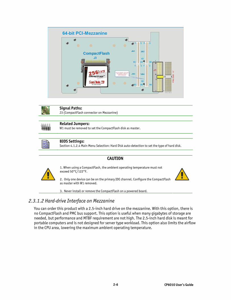
2-6 CP6010 User’s Guide
Signal Paths: J3 (CompactFlash connector on Mezzanine)
Related Jumpers: W1 must be removed to set the CompactFlash disk as master.
BIOS Settings: Section 4.1.2.4 Main Menu Selection: Hard Disk auto-detection to set the type of hard disk.
CAUTION
1. When using a CompactFlash, the ambient operating temperature must not exceed 50°C/122°F. 2. Only one device can be on the primary IDE channel. Configure the CompactFlash as master with W1 removed. 3. Never install or remove the CompactFlash on a powered board.
2.3.1.2 Hard-drive Interface on Mezzanine You can order this product with a 2.5-inch hard drive on the mezzanine. With this option, there is no CompactFlash and PMC bus support. This option is useful when many gigabytes of storage are needed, but performance and MTBF requirement are not high. The 2.5-inch hard disk is meant for portable computers and is not designed for server type workload. This option also limits the airflow in the CPU area, lowering the maximum ambient operating temperature.

2-7 CP6010 User’s Guide
64-bit PCI-Mezzanine
J1
Related Jumpers: Install W1 when using the hard drive.
Note: When using the hard disk, the maximum ambient operating temperature depends on the system’s airflow.
Signal Paths: The IDE port is available through IDE0, channel 0.

2-8 CP6010 User’s Guide
2.3.2 USB Interfaces USB strengths include:
• Capability to daisy chain as many as 127 devices per interface
• Fast bi-directional
• Isochronous/asynchronous interface
• 12MBPS transfer rate
• Standardization of peripheral interfaces into a single format
USB supports Plug and Play and hot-swapping operations (OS level). These features allow USB devices to be automatically attached, configured and detached, without reboot or running setup.
Signal Paths: USB0 signals are available on the faceplate from the J7 connector. Both USB 0 and USB 1 signals are available through the CPCI I/O connector (J3).
BIOS Settings: Advanced: Legacy USB Support (keyboard and mouse)
The CP6010 board supports the standard open host controller interface (OHCI) and uses standard software drivers that are OHCI compatible.
Pin Signal 1 VCC 2 DATA- 3 DATA+ 4 GND
PMC
12
Rea
dyto
Swap

2-9 CP6010 User’s Guide
2.4 Super I/O PC87471
2.4.1 Floppy Disk Interface The on-board floppy disk controller is IBM PC XT/AT compatible. It handles 3.5”, low and high density disks. It can support up to two drives in any combination.
Signal Paths: The floppy disk controller interface is available through the J5 connector.
BIOS Settings: Section 5.1.2.4, Main Menu Selection, Legacy Diskette A. Section 5.1.2.5.3, Advanced Menu Selection, On-board Device Configuration, Floppy Disk Controller.
2.4.2 PS/2 Keyboard / PS/2 Mouse Interface The on-board keyboard controller is compatible with 8042 software.
Signal Paths:
PS/2 keyboard and PS/2 mouse signals are available through the J3 CPCI I/O connector. Keyboard: J3, Row E, pin 2, 3. (See appendix for complete pinout description of J3.) Mouse: J3, Row E, pin 4, 5
BIOS Settings: Section 5.1.2.5.1, Advanced, Boot Settings Configuration Menu Selection, PS/2 Mouse.
2.4.3 Serial Ports Two fully functional serial ports are provided on the board for asynchronous serial communications. They are 16C550 high-speed UART compatible and support 16-byte FIFO buffers for transfer rates from 50bps to 115Kbps. Each serial port is specified as follows:
Designation Communication Mode Output Path Serial Port A (COM1) RS-232 Front Plate DB-9 (J6), CPCI J3
Serial Port B (COM2) RS-232/RS422/RS485 CPCI J3
UART registers are individually addressable and fully programmable.
2-10 CP6010 User’s Guide
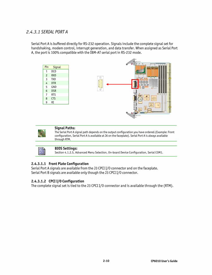
2.4.3.1 SERIAL PORT A
Serial Port A is buffered directly for RS-232 operation. Signals include the complete signal set for handshaking, modem control, interrupt generation, and data transfer. When assigned as Serial Port A, the port is 100% compatible with the IBM-AT serial port in RS-232 mode.
Signal Paths: The Serial Port A signal path depends on the output configuration you have ordered.(Example: Front configuration, Serial Port A is available at J6 on the faceplate). Serial Port A is always available through RTM.
BIOS Settings: Section 4.1.2.5, Advanced Menu Selection, On-board Device Configuration, Serial COM1.
2.4.3.1.1 Front Plate Configuration Serial Port A signals are available from the J3 CPCI I/O connector and on the faceplate. Serial Port B signals are available only though the J3 CPCI I/O connector. 2.4.3.1.2 CPCI I/O Configuration The complete signal set is tied to the J3 CPCI I/O connector and is available through the (RTM).
Pin Signal 1 DCD 2 RXD 3 TXD 4 DTR 5 GND 6 DSR 7 RTS 8 CTS 9 RI

2-11 CP6010 User’s Guide
2.4.4 Serial Port B Serial Port B is buffered directly for RS-232 operations and is 16C550 PC-compatible. The interface includes the complete signal set for handshaking, modem control, interrupt generation, and data transfer. This port is 100% compatible with the IBM-AT serial port.
Signal Paths: Serial Port B signals are only available through the J3 CPCI I/O connector.
Related Jumpers: W6 and W7: insert both jumper if Serial Port B is used in RS-422 or RS-485 mode and need termination resistors. Termination resistors are 120-ohm.
Bios Settings: Section 5.1.2.5.2.1, Advanced Menu Selection, On-board Device Configuration, Ethernet.
Upon a power-up or reset, the Serial Port B interface circuits is automatically configured for the operation mode setup in the BIOS. This Serial Port signal assignation on the J3 CPCI I/O connector depends on the operation mode (RS-232, RS-422, or RS-485) it has been set:
J3 Connector
Pin# Name RS-232 RS-422 RS-485
D3 DCD DCD RSV RSV
B3 RX RXD RX(-) RX/TX(-)
C3 DSR DSR RSV RSV
D4 TX TXD TX(-) RSV
A3 RTS RTS RX(+) RX/TX(+)
C4 CTS CTS TX(+) RSV
A4 RI RI RSV RSV
B4 DTR DTR RSV RSV
2.4.4.1 RS-232 Protocol When configured for RS-232 operation mode, the serial port is 100% compatible with the IBM-AT serial port signals.

2-12 CP6010 User’s Guide
2.4.4.2 RS-422 Protocol The RS-422 protocol (Full Duplex) uses both RX and TX lines during a communication session.
CAUTION
In RS-422 mode, install W6 and W7 jumper caps to connect the 120-Ohm termination resistors. (See the Jumper Settings section.)
2.4.4.3 RS-485 Protocol The RS-485 protocol (Half Duplex) also uses differential signals during a communication session. It differs from the RS-422 mode because it offers the ability to transmit and receive over the same pair of wires and allows a shared communication line by multiple stations. This configuration (also known as Party Line) allows only one system to take control of the communication line at a time. In RS-485 mode, the RX lines are used as the transceiver lines, and the RTS signal controls the direction of the RS-485 buffer. When set for RS-485 mode in the BIOS, upon power-up or reset, the transceiver is by default in receiver mode to prevent unwanted perturbation on the line. Party line operation mode requires termination resistors to be installed at both ends of the network.
CAUTION
When installing the board at one end of the network, connect the W6 and W7 jumper caps at the 120 ohms termination resistors (See Setting Jumpers).
2.5 Ethernet Interfaces The Ethernet (Intel 82546) controller resides on the Primary PCI bus and runs at 66MHz at 64-bit wide. The board can be ordered with the Copper or with the Optical Option. Each interface supports 10Base-T/100Base-TX/1000Base-T with auto-negotiation and automatic crossover cable detection, either in rear or front access depending on the ordered option. With the optical option, 1000Base-SX is available for front access configuration. The 82546 features high performance with TCP/IP and UDP/IP checksum offloading for IPv4 and IPv6, packet filtering, and jumbo frame up to 16K. The CP6010 has boot from LAN capability (PXE) on both ports, either in the copper or fiber mode. Enable the option from the BIOS Setup Program. Please refer to Section 4.1, PHOENIX BIOS Setup Program.
WARNING
This product may contain CLASS 1 LASER PRODUCT
See Kontron’s Web site: http://www.kontron.com for the latest drivers. See Intel’s Web site: http://www.intel.com for the latest drivers for the 82546EB and for additional information on the Ethernet controller.
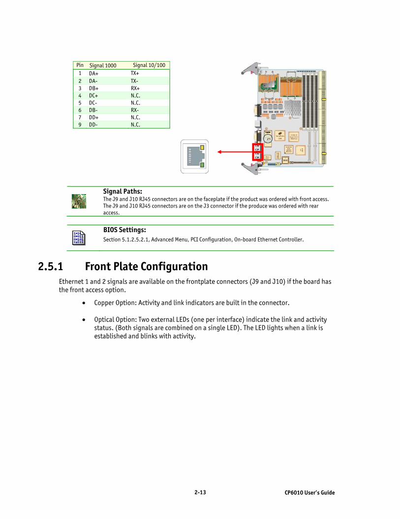
2-13 CP6010 User’s Guide
Signal Paths: The J9 and J10 RJ45 connectors are on the faceplate if the product was ordered with front access. The J9 and J10 RJ45 connectors are on the J3 connector if the produce was ordered with rear access.
BIOS Settings: Section 5.1.2.5.2.1, Advanced Menu, PCI Configuration, On-board Ethernet Controller.
2.5.1 Front Plate Configuration Ethernet 1 and 2 signals are available on the frontplate connectors (J9 and J10) if the board has the front access option.
• Copper Option: Activity and link indicators are built in the connector.
• Optical Option: Two external LEDs (one per interface) indicate the link and activity status. (Both signals are combined on a single LED). The LED lights when a link is established and blinks with activity.
Pin Signal 1000 Signal 10/100 1 DA+ TX+ 2 DA- TX- 3 DB+ RX+ 4 DC+ N.C. 5 DC- N.C. 6 DB- RX- 7 DD+ N.C. 9 DD- N.C.
2-14 CP6010 User’s Guide
2.5.2 CPCI I/O Configuration In rear access or 2.16 configuration, the two Ethernet ports are available from a RTM or in a PICMG2.16 system.
CAUTION
1. Front and rear panel configurations are not supported.
2. When using a PICMG2.16 system, LAN cannot be used on the RTM.
3. You cannot use a standard RTM with most PICMG2.16 systems. See your system’s manual.
Signal Paths: The Ethernet Ports signal paths depends on the output configuration you have ordered for the board. (Example: Front configuration, Ethernet ports are available at J9 and J10 on the faceplate). Ethernet Ports are always available through the RTM.
BIOS Settings: Section 4.1.2.5, Advanced Menu Selection, On-board Device Configuration, Ethernet.
2.6 System Management Features
2.6.1 Thermal Management The SBC includes a user-defined temperature sensor / alarm function, which provides thermal monitoring of the processor, using the ADM1026. In addition, the Pentium 4 includes an active thermal control circuit (TCC) that can automatically throttle the CPU clock when exceeding the maximum operating temperature. The current CPU temperature can be read by software or by a user application. Use the IPMI for increased system management. If you would like more information, please consult the IPMI section.
BIOS Settings: Section 5.1.2.6.1.3, Monitoring Menu Selection, Intelligent System Monitoring, Control Temperature Events.
CPU overheating may happen if the system fans fail. In the advent of catastrophic overheating, the SBC will power down itself.
Note: If the CPU overheats, the CPU asserts the THERMTRIP# signal, which stops power. You need to cycle BDSEL# (or remove and insert the board) to restart the board.

2-15 CP6010 User’s Guide
2.6.2 Power Supply Monitoring All on-board supplies are monitored; any low power rail holds the board in reset. Most power rails also can be monitored though the SM bus by using the ADM1026 or by using the embedded IPMI controller.
BIOS Settings: Section 5.1.2.6.1.2, Monitoring Menu Selection, Intelligent System Monitoring, Hardware Monitor Voltage Inputs.
2.6.3 Programmable Dual Stage Watchdog A two-stage digital watchdog timer with software programmable time-out period is available. Following a reset of any source, the watchdog is disabled. Software enables the watchdog.
Bios Settings: • Section 5.1.2.6, Monitoring Menu Selection.
• Enable watchdog automatically before OS launch.
Bios Settings: • Section 5.1.2.6, Monitoring Menu Selection
• Watchdog After POST
• Watchdog Duration
• FPGA IRQ
Software Usage: • See registers 0x190 and 0x196 description in Appendix C for details.
• See Application Note AN030001A for watchdog timer usage.

2-16 CP6010 User’s Guide
2.7 Video Interface The video controller, CT69030, with its integrated 4Meg of high performance SDRAM is capable of CRT resolutions up to 1600 x 1200 x 65K colors (4MB RAM). The video interface features 64-bit 2D graphics engine, 64-bit GUI accelerator engine with multiple window video acceleration.
Signal Paths: In front I/O configuration: J8 on the faceplate. In rear I/O configuration: J3 CPCI connector.
Related Jumpers: W8 enables or disables the on-board VGA feature. See Section 3.1 – Jumper Settings.
BIOS Settings: Section 5.1.2.5.2, Advanced Menu selection, PCI Configuration, Default Primary Video Adapter.
Front Plate Configuration
VGA interface signals are available on the J8 connector, the standard VGA connector, located on the faceplate if the board has front access operations. This configuration allows direct connection of CRT display to the board.
CPCI I/O Configuration VGA interface signals are available on the J3 CPCI I/O connector if the board has rear panel output operations.
2.7.1 Supported Resolutions The maximum video resolution and performance depend directly on the drivers running with your software application. Resolution and number of colors specification are listed below:
Resolution Number of Colors
640x480, 800x600, 1024x768, 1280x1024, 1600x1200 256 (8 bits)
640x480, 800x600, 1024x768, 1280x1024, 1600x1200 65,536 (16 bits)
640x480, 800x600, 1024x768, 1280x1024 16.8 million (24 bits)
640x480, 800x600, 1024x768 16.8 million (32 bits)

2-17 CP6010 User’s Guide
2.7.2 Major Features Description
VGA Compatibility
The video controller includes all registers and data paths required for the VGA controller and supports extensions to VGA, including resolutions up to 1600 x 1200 x 65K colors non-interlaced. The 24-bit images are displayed at up to 1280x1024 resolution.
2D Graphics Engine
The 2D graphics engine is an advanced 32-bit, three-operand engine that accelerates BitBLTs as line draws, polygon draw, and polygon fill. The 2D graphics engine also performs video and bitmap scaling, and data overlay.
2.8 CPCI Features
2.8.1 Universal Bridge (PLX6540) This cPCI product’s access to the backplane bus runs through the PLX PCI to PCI universal bridge. The feature set of this bridge is similar to the HB6 and HB8, which is used on Kontron cPCI products. The PLX can operate in either 32 or 64 bits bus width and with any PCI frequency up to 66MHz.
2.8.1.1 Transparent Mode When the CP6010 is inserted in the system slot of a backplane, the bridge is configured in transparent mode and performs like any other bridge. You can configure important registers from the BIOS setup.
2.8.1.2 Nontransparent Mode If the SBC is inserted in a peripheral slot, the PLX will be configured in nontransparent mode and will be seen as an I/O device. By default, it will appear with vendor ID 10B5h and device ID 6540h. The PLX will always claim a 16MB window unless the default is changed in the EEPROM settings.
2.8.1.3 Busless Operation When used in a busless slot, as in some PICMG2.16 systems, the bridge will be disabled and will disappear from the PCI device list.
2.8.1.4 Using the EEPROM If you use this product as an I/O board, you can assign different vendor ID and device ID to the PLX and can configure the PCI resources that will be claimed at boot up. This allows the CP6010 to act as an I/O board, like any other peripheral device (SCSI, Ethernet) and to load proper drivers. Please contact Kontron’s technical support if you need to configure the EEPROM.

2-18 CP6010 User’s Guide
Related Jumpers: W15-W16-W18 allow you to set maximum bus speed or disable the bridge.
Bios Settings: Section 5.1.2.5.2.3, Advanced Menu Selection, PCI Configuration, PCI Performance settings, HB8 related options.
2.8.2 Hot Swap
2.8.2.1 Power Ramping and Overcurrent Protection This product has electrical components that control current ramp-up on the board when the board is hot swapped in the chassis. Current transient upon insertion follows the PICMG2.1R2.0 specification. The hot swap circuit also protects from overcurrent. If for any reason current requirements increase to an abnormal level, the board will shut down. Power cycling or board select (BDSEL# signal) cycling restarts the board.
2.8.2.2 Hardware Connection Process If you would like more information, please see Section 1.5.4 for technical background. This section explains how to use the ENUM# signal. When the board is used in a system slot, it is possible to detect insertion and pending extraction of a compliant peripheral cPCI card.
WARNING
1. Some mechanical parts of the guide-rail are fragile (shield contacts and clips). Do not use force to insert and connect a CompactPCI module.
2. If there is any mechanical resistance while you insert a module, ensure there is no mechanical obstacle and verify that all parts are well aligned.
2.8.3 Bus Mode The PICMG2.0R3.0 specification and PICMG2.1R2.0 specification do not dictate how to support a PCI-X card. This product implements a solution that is the best candidate for the next revision of this specification. Bus-speed negotiation is always done on a PCI reset. Inserting a board in a live system will never make the bus not function with compliant hardware. A peripheral card will have a problem if the bus is faster than the card’s capability. In other cases, the card should initialize itself with the current bus mode.

2-19 CP6010 User’s Guide
2.9 IPMI This product fully supports Intelligent Platform Management Interface 1.1 (IPMI 1.1) and PICMG2.9R1.0 specifications. It uses a 16-bits micro-controller (Hitachi H8/2148) to run an IPMI firmware.
2.9.1 Technical Background IPMI is an extensible and open standard that defines autonomous system monitoring. It is autonomous because all satellite devices send warnings and critical events to a baseboard management controller (BMC) that logs it to a system event log (SEL). This standardized management interface also allows the user’s system management software (SMS) to discover a system’s components and to build a database of all present sensors to monitor them and detect critical condition. You can find more information about the IPMI at the following Web sites: http://www.intel.com/design/servers/ipmi/spec.htm http://www.intel.com/design/servers/ipmi/ http://www.intel.com/platforms/applied/eiacomm/papers/25133701.pdf
2.9.1.1 IPMI Glossary
IPMI Intelligent Platform Management Interface
BMC
Baseboard Management Controller In a compact PCI chassis, there can be only one BMC present. The BMC includes de SEL and the SDRR for the complete system. The BMC is connected to the other blades in the system via the dual port IPMB interface. The board firmware can be set in BMC by selecting the option in the BIOS setup menu.
Satellite In a compact PCI chassis, threre can be many satellites. Each satellite is connected to the other blades via the dual port IPMB interface. The board firmware can be set in satellite mode by selecting the option in the BIOS menu.
SEL System Event Log The SEL repository is present only in the BMC. If an event occurs in any blade, the sensor event is sent throught the IPMB bus (if SEL is not local) and stored in the BMC SEL repository.
SDR Sensor Data Record
SDRR
Sensor Data Record Repository ( The SDRR is only present in the BMC. Normally, the SDRR contains all sensor records of the chassis. A utility named ‘fillsf.exe’ is provided in the IPMI DOS tool package to make a full chassis discovery and fill the SDRR with the found sensor records. A new board contains all the local sensors in the SDRR.
IPMB Intelligent Platform Management Bus
KCS Keyboard Controller Style
FRU
Field Replaceable Units A FRU is available in BMC or satellite mode. The FRU contains information about the product such as the part number and the serial number. See PICMG Specification 2.9 for complete details on the FRU byte structure. Use Fillsf.exe to update the FRU.
SMS System Management Software

2-20 CP6010 User’s Guide
2.9.1.2 IPMI in a Compact PCI Chassis IPMI implementation in cPCI environment is defined by the PCMIG2.9R1.0 specification. The specification gives the pinout of J1 and J2 as well as the addressing scheme. There should be only one BMC in the chassis, or at least on the IPMIB segment). The BMC may reside either on an SBC blade or on an external system management card (SMC), the specification gives full latitude over this.
( 1 ) IPMB address for satellite is determined via the location of the slot in the chassis.
2.9.1.3 IPMI Setup To use the IPMI resources in a system, some steps are needed. The system operator must take Step 1. The SMS application performs Steps 2 and 3.
1. Elect a BMC by setting the mode to BMC in the BIOS Setup Menu. By default, all Kontron’s CPCI blades are configured in satellite mode.
2. Fill the SDRR with all the present sensors in the chassis. This step may be done using the fillsf.exe utility in DOS. The SDRR must be rebuild each time there is a configuration change in the chassis.
3. Probe the BMC SEL for event or any other available information using the SMS of your choice or by sending the command directly using the available tools.
2.9.2 IPMI Implementation of CP6010
2.9.2.1 Features
• Compliant with IPMI specification 1.0, revision 1.1
• Compliant with PICMG 2.9 specification
• Can be configured as BMC or Satellite by software from the BIOS Setup Menu
BMC IPMB Address
Fix: 20h
Satellite IPMB Address:
B6h(1)
Satellite IPMB Address:
B8h(1)
Satellite IPMB Address:
B2h(1)
Satellite IPMB Address:
B0h(1)
Satellite IPMB Address:
BAh(1)
Satellite IPMB Address:
B4h(1)
Satellite IPMB Address:
BCh(1)
IPMB 0
IPMB 1

2-21 CP6010 User’s Guide
• Firmware designed and specially made for compact PCI implementation
• KCS SMS interface with interrupt support
• Dual Port IPMB configurable as two independent channels or in redundant mode BIOS Setup Menu
• Out of band management and monitoring using IPMB interface permits access to sensors regardless of SBC state
• Sensor threshold fully configurable
• Complete IPMI watchdog functionality
• Complete SEL, SDR repository and FRU functionality
• Master Read/Write I2C supports for external I2C devices communications (FRU, EEPROM, FAN)
• Firmware can be updated in the field
• Firmware fully customizable per customer needs
• Interoperable with other IPMI solution
2.9.2.2 Sensors Implemented on CP6010 The IPMI firmware includes many sensors. This product implements 37 sensors, some for voltage and current monitoring and others for pass/fail type signal monitoring. Each sensor’s description is built in the IPMI firmware and is accessible to the SMS. The following signals are implemented on the CP6010: Sensors Precision Description Voltage 5V ±1% Board 5V supply Voltage 3.3V ±1% Board 3.3V volts supply
Voltage 2.5V ±1% On board DC-DC converter from 3.3V. Mainly used for memory.
Voltage 1.5V ±1% On-board DC-DC converter from 3.3V. Mainly used by chipset and Ethernet controller.
Voltage 12V ±1% Board 12V supply. (1) Voltage –12V ±1% Board –12V supply. (1) Voltage battery ±1% Board RTC battery. (1)
Current Icc 5V ±7% Total current from baseboard and mezzanine on 5V supply.
Current Icc 3.3V ±7% Total current from baseboard and mezzanine on 3.3V supply.
Balance Icc 5V ±7% Difference between baseboard and mezzanine current on 5V supply.
Balance Icc 3.3V ±7% Difference between baseboard and mezzanine current on 3.3V supply.
Temperature board ±1% Current board temperature under CPU1. (1)
Temperature CPU1 ±1% Current CPU temperature, on-die thermal diode. (1)

2-22 CP6010 User’s Guide
Temperature CPU2 ±1% Current CPU temperature on-die thermal diode (1)
LAN heartbeat LAN0 link NA LAN0 link status (PCI bus 1, device 5 function 0)
LAN heartbeat LAN1 link NA LAN1 link status (PCI bus 1, device 5 function 1)
Oem reset NA Indicates current source holding board in reset
Watchdog 2 NA IPMI watchdog Processor CPU1 status NA Presence indication of CPU1 Processor CPU2 status NA Presence indication of CPU2 Processor CPU1 hot NA Thermal over heat indication Processor CPU2 hot NA Thermal over heat indication
Power supply PSU status NA ???
Power supply board select NA Reflect board select input signal status.
Power supply power good NA Reflect goodness of various on board supply
Power supply switcher en. NA
Processor CPU VID good NA Can be false if two CPU with difference VID are installed
Entity presence: system slot NA Indicated is board is in a system slot
Critical interrupt: NMI NA
Critical interrupt: SMI timeout NA
Module/board: board ejector NA
Cable interconnect: IPMB1 alert NA PICMG 2.9 required sensor
Cable interconnect: IPMB0 stuck NA PICMG 2.9 required sensor
Cable interconnect: IPMB1 stuck NA PICMG 2.9 required sensor
OEM firmware: IPMI info-1 NA
OEM firmware: IPMI info-2 NA
OEM RunInitAgent:Agent err NA
2.9.3 Software Support
2.9.3.1 IPMI KCS Support in Different OS IPMI is still an emerging standard for system management. There are few easy to used tools as of today. Linux
An open source KCS driver is available for Linux at http://openipmi.sourceforge.net. This driver includes all the necessary functionality (and more) to communicate with the firmware. Intel provides some Linux KCS reference drivers; they are available at the following address: http://www.intel.com/design/servers/ipmi/ipmi_driver.htm. Contact Kontron’s technical support for additional tools or help with Linux IPMI tools.
Windows
Intel provides some Windows KCS reference drivers; they are available at the following address: http://www.intel.com/design/servers/ipmi/ipmi_driver.htm

2-23 CP6010 User’s Guide
2.9.3.2 Firmware Update
A DOS IPMI tool package is available from Kontron and includes the utility ipmifwu (IPMI firmware update). This utility allows you to upload a new binary file to the Management Controller. Consult the ipmifwu usage display for complete utility options (by running ipmifwu–h). Visit the Kontron Web site for package and firmware availability or call Kontron Technical Support. Firmware update procedure:
1. Boot DOS. 2. Place both firmware binary and utility ‘ipmifwu.exe’ on a floppy. 3. Insert the floppy and run the following: ipmifwu –f firmware.bin –p –r
WARNING
Some firmware might not be compatible with some BIOS versions. Always upgrade the BIOS and firmware as recommended.
2.10 Debugging Features
2.10.1 Bi-color Debug LED The board has a bi-color LED that is very useful to debug. (Consult the quick reference sheet.) The significance of the LED is context dependent and is shown below.
Time LED usage
During reset and prior to FPGA programming. RED is ON. No blinking.
After reset, during the boot process. Postcode blinker (blinking)
After the boot process, while the operating system loads. GREEN reflects hard-disk activity; RED is not used.
Application software does not use the LED.
GREEN reflects hard-disk activity; and RED is not used. While the application software runs.
Application software uses the LED to display status information.
Software Usage: See register 0x19A description in Appendix C for details.
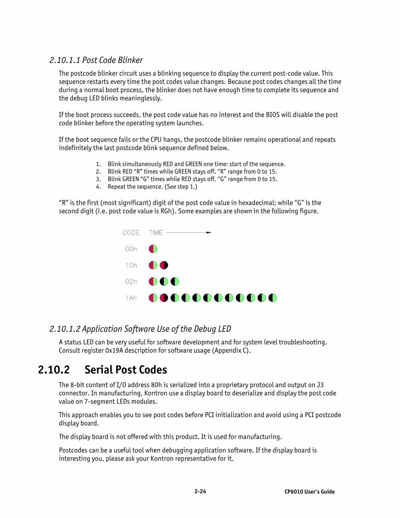
2-24 CP6010 User’s Guide
2.10.1.1 Post Code Blinker The postcode blinker circuit uses a blinking sequence to display the current post-code value. This sequence restarts every time the post codes value changes. Because post codes changes all the time during a normal boot process, the blinker does not have enough time to complete its sequence and the debug LED blinks meaninglessly. If the boot process succeeds, the post code value has no interest and the BIOS will disable the post code blinker before the operating system launches. If the boot sequence fails or the CPU hangs, the postcode blinker remains operational and repeats indefinitely the last postcode blink sequence defined below.
1. Blink simultaneously RED and GREEN one time: start of the sequence. 2. Blink RED “R” times while GREEN stays off. “R” range from 0 to 15. 3. Blink GREEN “G” times while RED stays off. “G” range from 0 to 15. 4. Repeat the sequence. (See step 1.)
“R” is the first (most significant) digit of the post code value in hexadecimal; while “G” is the second digit (i.e. post code value is RGh). Some examples are shown in the following figure.
2.10.1.2 Application Software Use of the Debug LED A status LED can be very useful for software development and for system level troubleshooting. Consult register 0x19A description for software usage (Appendix C).
2.10.2 Serial Post Codes The 8-bit content of I/O address 80h is serialized into a proprietary protocol and output on J3 connector. In manufacturing, Kontron use a display board to deserialize and display the post code value on 7-segment LEDs modules.
This approach enables you to see post codes before PCI initialization and avoid using a PCI postcode display board.
The display board is not offered with this product. It is used for manufacturing.
Postcodes can be a useful tool when debugging application software. If the display board is interesting you, please ask your Kontron representative for it.
2-25 CP6010 User’s Guide
2.10.3 Reset History When an unwanted reset of the board occurs, it is interesting to know the reset source. The reset history circuit logs reset sources. There are two ways to obtain the reset history:
• Let the BIOS read and clear the reset history and display the reset source in the summary screen.
• End-user software reads and clears the reset history.
In addition, the IPMI controller sends events to the system’s baseboard management controller (BMC). By reading the SEL, you can determine which event resets the board. Please consult the IPMI section for further details.
BIOS Settings: • Monitoring Setup Selection.
• Display and Clear Reset History
Software Usage: See registers 0x191 and 0x192 description in appendix C for details.
2.11 Miscellaneous Features
2.11.1 Simple I2C Controller The CP6010 offers a simple, master-only I2C controller. It can be used to access an on-board EEPROM. A bit-banging interface also is provided.
Software Usage: • See registers 0x1A8 through 0x1AC in Appendix C for details.
• See Application Note AN03002A for I2C controller usage and a software example.
2.11.2 Serial Number A DS2401 silicon serial number comes standard on the CP6010. It can be read from register 0x193. (See appendix C).
3-0 CP6010 User’s Guide
3. Installing the Board Contents
3.1 Setting Jumpers ..........................................3-1 3.2 Processor ...................................................3-3 3.3 Memory......................................................3-3 3.4 On-board Interconnectivity............................3-5 3.5 Backup Battery ............................................3-7 3.5 Backup Battery ............................................3-7 3.6 Board Hot Swap and Installation .....................3-8

3-1 CP6010 User’s Guide
3.1 Setting Jumpers
3.1.1 Jumper Description
Description
CompactFlash Setting Configure Compact Flash or 2.5” hard disk in master mode. W1
Clear CMOS On position 1-2, all CMOS information is cleared. This jumper is not set by default. This jumper must be installed to force a BIOS Flash update with the hot key sequence (Ctrl-E).
W2
Test Mode COM2 is used to output post code. Also prevents BMC from generating interrupts. Used for Kontron’s test environment only.
W3
VT-100 Access When enabled, allows VT100 or ANSI terminal connection (data serial download from a remote computer). W4
BMC Reset Enables or disables the BMC. W5
Serial COM2 Termination Use these jumpers to connect or disconnect the termination resistors on/from Serial COM2 when set for RS-422/RS-485 operation mode 0.
W6
W7
On-board Video Use this jumper to disable the on-board video feature. W8
Reserved When installed, board will turn on without power from mezzanine. This option is used in Kontron’s production tests
W9
PMC PCI Maximum speed Sets the maximum speed (66/100/133MHz) of PCI bus located on the Mezzanine. W13 W14 W15
Backplane PCI Sets the maximum speed (33/66MHz) of the PCI bus located on the backplane W16 W17 W18
On-board Battery Connects or disconnects the battery to/from board circuitry.
W19

3-2 CP6010 User’s Guide
3.1.2 Setting Jumper & Locations

3-3 CP6010 User’s Guide
3.2 Processor This product ships with the CPU installed and a thermal solution. Because the thermal solution is a custom one and the thermal interface is critical for passive cooling, Kontron does not guarantee thermal performance if the heat sink is removed and then reinstalled by the end user. If you need to upgrade the CPU, contact Kontron’s technical support.
3.3 Memory Only use validated memory with this product. Currently recommended part numbers are: Manufacturer Part Number Description Company M312L6420CT0-CA200 DIMM ECC RSDRAM 512MB 64M*72 DDR266 1.2" SAMSUNG M312L6420DT0-CA200 DIMM ECC RSDRAM 512MB 64M*72 DDR266 1.2" SAMSUNG UG764D7584KM-EZKA DIMM ECC RSDRAM 512MB 64M*72 DDR266 1.2" UNIGEN VM383L6420E-A2S DIMM ECC RSDRAM 512MB 64M*72 DDR266 1.2" VIRTIUM UG7128D7584KV-EZKA DIMM ECC RSDRAM 1GB 128M*72 DDR266 1.2" UNIGEN M312L2828DT0-CA200 DIMM ECC RSDRAM 1GB 128M*72 DDR266 1.2" SAMSUNG M312L2828CT0-CA200 DIMM ECC RSDRAM 1GB 128M*72 DDR266 1.2" SAMSUNG VM383L2826E-A2S DIMM ECC RSDRAM 1GB 128M*72 DDR266 1.2" VIRTIUM M312L3223DT0-CA200 DIMM ECC RSDRAM 256MB 32M*72 DDR266 1.2" SAMSUNG UG732D7588KZ-DZKA DIMM ECC RSDRAM 256MB 32M*72 DDR266 1.2" UNIGEN M312L3223DT0-CB0 DIMM ECC RSDRAM 256MB 32M*72 DDR266 1.2" SAMSUNG VM383L3223E-B0S DIMM ECC RSDRAM 256MB 32M*72 DDR266 1.2" VIRTIUM M312L3223CT0-CA200 DIMM ECC RSDRAM 256MB 32M*72 DDR266 1.2" SAMSUNG UG7256D75Q4MQ-EZKA DIMM ECC RSDRAM 2GB 256M*72 DDR266 1.2" UNIGEN VM383L5626E-A2S DIMM ECC RSDRAM 2GB 256M*72 DDR266 1.2" VIRTIUM M312L5628MT0-CA200 DIMM ECC RSDRAM 2GB 256M*72 DDR266 1.2" SAMSUNG Memory should have the following characteristics:
• DDR200 or DDR266
• 2.5V only
• Single-sided or double-sided
• X4 or X8 configuration supported
• Serial Presence Detect (SPD) EEPROM
• 64-bit and 72-bit DIMMs supported
• 1.2 inch maximum height

3-4 CP6010 User’s Guide
WARNING
Because static electricity can cause damage to electronic devices, take the following precautions: • Keep the board in its anti-static package, until you are ready to install
memory. • Wear a grounding wrist strap before removing the board from its package;
this will discharge any static electricity that may have built up in your body. • Handle the board by the faceplate or its edges.
3.3.1 Installing Memory
On an anti-static plane, place the board so that you face the DIMM sockets and the faceplate is facing you.
Insert the DIMM into J17 and J18 then in J15 and J16. The memory must be installed in pairs. To install a DIMM, align the notche on the module with the socket’s key inserts.
Push the DIMM in angle (right side first) into the socket until the left retaining clip snap on.
Repeat these steps to add other memory sockets.
To remove a DIMM from a socket, push downw the left retaining clip of the socket. Pull the module up from the left to remove.
Note: The right ejector won’t move during the operation because of mechanical restrictions due to the mezzanine

3-5 CP6010 User’s Guide
3.4 On-board Interconnectivity
3.4.1 On-board Connectors and Headers Description Connector Comments
CompactPCI Bus J1/J2 J1- CPCI bus signals and power. J2- 64 bit extension, arbitration, clocks, reset and power.
CompactPCI I/O J3 Serial Ports A and B, LAN 0 and 1, PS/2 Keyboard and Mouse, VGA, and USB.
CompactPCI I/O J4 (SCSI) SCSI (SCSI board version).
CompactPCI I/O J4 (PIM) Mezzanine signals (PIM board version).
CompactPCI I/O J5 Legacy connections (IDE and Floppy).
Serial Port A J6 Supports standard 9-pin DSUB male connector (faceplate).
USB2 J7 4-pin USB connector (faceplate).
VGA J8 Supports standard 15-pin DSUB female connector (faceplate).
Ethernet LAN1 J9 RJ-45 connector with built-in activity and link indicators (faceplate)
Ethernet LAN2 J10 RJ-45 connector with built-in activity and link indicators (faceplate)
Reset SW1 Reset Switch (faceplate)
Thes
e co
nnec
tors
are
lo
cate
d on
face
plat
e
CPU Sockets J13, J14 mPGA604 sockets
Memory Sockets J15-J18 DIMM 184-pin (Registered DDR-200/266 SDRAM)
Hot Swap J20 Hot Swap Switch
POST Code J21 4-pin locking (not populated)
Power J22 2-pin non locking (VCC3)
Storage Mezzanine J23 Supports Kontron’s module dedicated to CompactFlash disks
PCI Mezzanine JN1-JN4 64-Bit PCIX Mezzanine
Battery BT1 CMOS backup battery connector

3-6 CP6010 User’s Guide
3.4.2 Front Plate Connectors and Indicators
Name Description Comments
J6 Serial Port A Standard 9-pin DSUB male connector.
J7 USB2 4-pin standard USB connector.
SW1 Reset Button Use a small tool to press the button and proceed to a hardware reset of the board.
J8 Video Connector Standard 15-pin DSUB female connector.
J9, J10 LAN1 and LAN2 Ethernet RJ-45 connectors with built-in activity and link indicators or SFF LC optical transceiver.
Blue LED Ready to Swap Lights when the board is ready to be swapped.
Green LED HDD Activity Indicates an activity on IDE.
PMC Mezzanine The front plate supports a PMC cutout and a cap that also acts as an EMI shield when there are no PMC devices installed.
Copper Option Optical
Option
Activity and link indicator for LAN 2
Activity and link indicator for LAN1

3-7 CP6010 User’s Guide
3.5 Backup Battery An on-board 3.6V lithium battery is provided to back up BIOS setup values and the real time clock (RTC). When replacing, the battery must be connected as follows:
1. Place your index and thumb at each side of the battery and gently pull out the battery. 2. Insert a new one firmly in place with respect to the positive and negative location of the
pins.
WARNING
There is a danger of explosion if you replace the battery incorrectly. Replace the battery with the same or equivalent type recommended by the manufacturer. Dispose of used batteries according to the manufacturer's instructions. When you receive a board, remove the on-board battery jumper to enable the battery. (See Section 3: Jumper settings.)

3-8 CP6010 User’s Guide
3.5.1 Operation and Preventative Maintenance The operational battery voltage must be between 2.9 and 3.6 volts. When the board is stored and is kept in it's original package, the battery must be replaced when the battery voltage is below 2.9 volts. For preventive operational maintenance, we recommend to verify the battery voltage after 4 years. After that period, we recommend that the safety voltage is checked more often. The normal battery life expectancy depends on the utilisation of the board.
• Kontron ordering MRP: 100-001
• Tadiran ordering MRP: 15-51-86-420-007 (TL-5186)
3.6 Board Hot Swap and Installation Because of the high-density pinout of the hard-metric connector, some precautions must be taken when connecting or disconnecting a board to/from a backplane:
1. Rail guides must be installed on the enclosure to slide the board to the backplane. 2. Do not force the board if there is mechanical resistance while inserting the board. 3. Screw the frontplate to the enclosure to firmly attach the board to its enclosure. 4. Use extractor handles to disconnect and extract the board from its enclosure.
Note: Hot swap of the CP6010 in a system slot is not defined. This results in a cold start of the system.
WARNING
Always use a grounding wrist wrap before installing or removing the board from a chassis.
WARNING
Removing the system host in a running system can harm some PCI I/O devices because the bus remains floating. At least, PCI reset should stay asserted, but not all systems detect this condition and hold reset active when no system slot is present.

3-9 CP6010 User’s Guide
3.6.1 Installing the Card in the Chassis To install a card in a chassis:
1. Remove the filler panel of the slot or see “Removing the Card” below. 2. Ensure the board is configured properly. 3. Carefully align the PCB edges in the bottom and top card guide. 4. Insert the board in the system until it makes contact with the backplane
connectors. 5. Using both ejector handles, engage the board in the backplane connectors until
both ejectors are locked. 6. Fasten screws at the top and bottom of the faceplate.
3.6.2 Removing the Board If you would like to remove a card from your chassis please follow carefully these steps:
1. Unscrew the top and the bottom screw of the front panel. 2. Push the red handle latch until the ejector fall free. 3. Using both ejectors, disengage the board from the backplane. 4. Pull the board out of the chassis.
3.6.3 Installing a PMC Card To install a PMC card:
1. Remove the mezzanine from the baseboard. 2. Unscrew the four screws that retain the mezzanine to the board. 3. Carefully pull out the mezzanine to disengage all connectors.
To install the PMC on the mezzanine:
1. Carefully push the PMC to mate the four connectors. 2. Screw the four screws at the bottom of the PMC to fix it to the mezzanine.
To reinstall the mezzanine:
1. Carefully engage the front plate part of the PMC into the baseboard’s face plate opening.
2. Push the mezzanine to engage the IDE extension connector, which is the more fragile of the connector set.
3. Put back the four screws to hold the mezzanine in place.

3-10 CP6010 User’s Guide
3.6.4 Installing a CompactFlash or Hard Drive This product supports all type I and type II CompactFlash modules.
WARNING
Never install or remove the compact flash while the board is on.
To install the CompactFlash:
1. Remove the plastic retainer. 2. Insert the CompactFlash in place. 3. Reinstall the plastic retainer.
To remove the CompactFlash:
1. Remove the plastic retainer. 2. Pull the CompactFlash module out. If it is needed, remove the PMC mezzanine
before removing the CompactFlash. If you have to remove the PMC, consult the previous section.
3. Install a new CompactFlash module. 4. Reinstall the plastic retainer

4-0 CP6010 User’s Guide
4. Building a CPCI System Contents
4.1 Building a CPCI System..................................4-1 4.2 CPCI I/O Signals...........................................4-6

4-1 CP6010 User’s Guide
4.1 Building a CPCI System The basic components needed to build a CompactPCI system include:
• Chassis
• Backplanes
• Power supplies
• Ventilation unit
• System, peripheral or busless boards following application requirements
• Other accessories such as storage modules, Ethernet switches, system management cards, and RTM
See your system’s manual for more details.

4-2 CP6010 User’s Guide
4.1.1 Backplane The CP6010 board draws a lot of power from the backplane. For that purpose, the mezzanine should always fall in a slot where J1 is populated. In other cases, the board will not power up. This imposes some restrictions on the backplane, which you can use with the CP6010. For example, the CP6010 cannot be used in the system slot of an eight-slot, right-adjusted backplane unless there is a ninth slot for the mezzanine. The CP6010 is fully compatible with the XL-PSB, XL-LP42 and XL-VHDS. When building a XL-VHDS configuration, allow a slot for the mezzanine. If using a third party system, consult you system’s manual determine the system’s compatibility with the CP6010. J1 and J2 connectors must be compatible with PICMG2.0R3.0
Note: J1 and J2 are de-facto industry standard as defined by PICMG2.0R3.0. The J3 connectors is user defined. Pinouts vary from vendor to vendor. Backplanes should be feed-through with the exception of PICMG2.16R1.0 compliant system, which routes Ethernet signals into the backplane. J4 and J5 are defined by users and vary from vendor to vendor and should be feed-through. Systems that do not meet this requirement may permanently damage the CP6010. Contact Kontron Technical Support to verify pinout compatibility with other chassis backplanes.
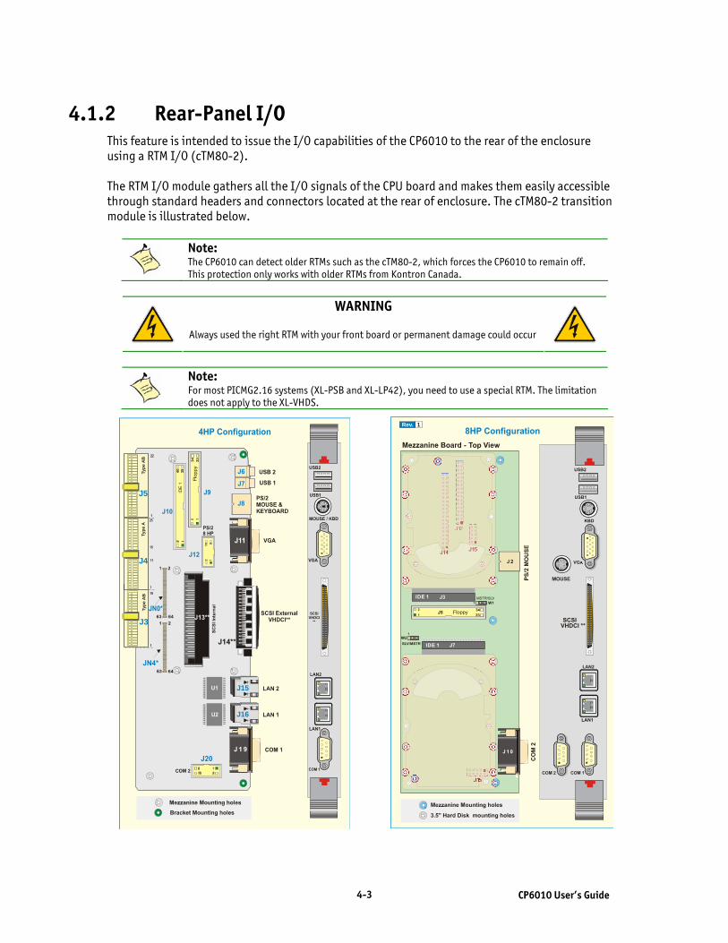
4-3 CP6010 User’s Guide
4.1.2 Rear-Panel I/O This feature is intended to issue the I/O capabilities of the CP6010 to the rear of the enclosure using a RTM I/O (cTM80-2). The RTM I/O module gathers all the I/O signals of the CPU board and makes them easily accessible through standard headers and connectors located at the rear of enclosure. The cTM80-2 transition module is illustrated below.
Note: The CP6010 can detect older RTMs such as the cTM80-2, which forces the CP6010 to remain off. This protection only works with older RTMs from Kontron Canada.
WARNING
Always used the right RTM with your front board or permanent damage could occur
Note: For most PICMG2.16 systems (XL-PSB and XL-LP42), you need to use a special RTM. The limitation does not apply to the XL-VHDS.
Type
AB
Type
AB
Type
A
J3
J4
J5
J15
J16
1Rev.

4-4 CP6010 User’s Guide
4.1.3 Storage Devices A mezzanine card that supports CompactFlash or 2.5-inch hard drives is attached to the system processor. If more storage devices or DVD/floppy drives are needed, 6U form factor storage modules are supported with the XL-VHDS system. 3U SCSI trays also are supported in VHDS for very high storage capacity and very high MTBF. This requires a SCSI PMC. Consult you system’s manual for available storage device.
4.1.4 Power Supply Use of 3U or 6U Compact PCI power supplies is strongly recommended with the CP6010. Although you can use other power supply types, make sure they can handle the power requirement, current transient, and voltage tolerance. Use of an ATX power supply is not recommended. 3U and 6U CompactPCI power supply modules feature load sharing redundant mode and hot-swap capabilities, which allow on-site replacements of defective modules while the system remains on.
4.1.5 Connector Keying CompactPCI connectors support guide lugs to ensure a correct polarized mating. A proper mating is enhanced by the use of color-coded keys for 3.3V and 5V operation. Color-coded keys prevent inadvertent installation of a 5V peripheral/system board in a 3.3V slot. The CP6010 is universal in this respect, so there is no color key in J1. However, always key backplanes in accordance to their VIO settings. Note that 5V signaling forces a 33MHz PCI bus mode. When operating at 3.3V, all PCI frequencies are valid.
Signaling Voltage Key Color
3.3V Cadmium Yellow
5V Brilliant Blue
Universal board (5V and 3.3V)
None
Keying also is defined in the J4 connector to determine its usage. CP6010 supports user I/O on J4 so it is keyed with the nut-brown key. Backplanes that feed through J4 also have a brown key. Other J4 usages have their key defined in PICMG2.10R1.0.
J4 Usage Key Color
User I/O Nut Brown
H.110 Strawberry Red
Standard switch Blue Lilac
Extended switch
Ocher Yellow
Cavity keying within the card guide and handle is used to protect J2, J3 and J5 usage. The CP6010 is keyed accordingly to PICMG2.10R1.0 and PICMG2.16R1.0. Few systems support this keying so you must take care to verify the type of slot before installing the board. XL-VHDS features complete keying and offers the greatest protection against pinout mismatch.

4-5 CP6010 User’s Guide
4.1.6 Bus Mastering The CP6010 provides seven pairs of REQ/GNT (0-6) arbitration signals through the secondary PCI bus. This means that the board can drive up to seven CPCI slots with PCI bus master capabilities. CPCI I/O Signals This section describes integrated feature signals available on rear panel CPCI I/O connectors (J3, J4, and J5).
4.1.7 CompactPCI Connectors
CPCI J5 Connector
Legacy connections (IDE, Floppy)
CPCI J4 Connector
SCSI Ultra-160/320 connections (SCSI board version) or PIM connections ( PIM board version)
CPCI J3 Connector
LAN0 and LAN1, Serial Ports A and B, PS/2 Keyboard and Mouse, VGA, POST, ID, Speaker, and USB.
CPCI J2 Connector
64-bit extension, arbitration, clocks, reset, and power. CPCI J1 Connector
Supports CPCI bus signals and power.
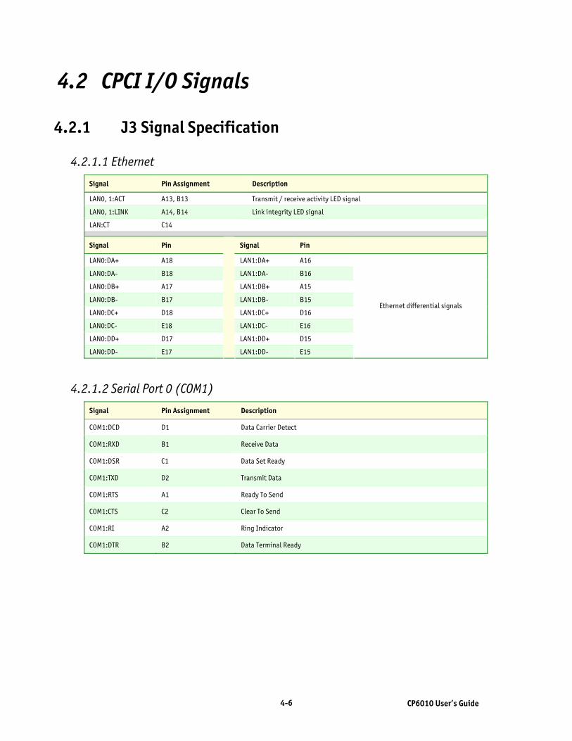
4-6 CP6010 User’s Guide
4.2 CPCI I/O Signals
4.2.1 J3 Signal Specification
4.2.1.1 Ethernet
Signal Pin Assignment Description
LAN0, 1:ACT A13, B13 Transmit / receive activity LED signal
LAN0, 1:LINK A14, B14 Link integrity LED signal
LAN:CT C14
Signal Pin Signal Pin
LAN0:DA+ A18 LAN1:DA+ A16
LAN0:DA- B18 LAN1:DA- B16
LAN0:DB+ A17 LAN1:DB+ A15
LAN0:DB- B17 LAN1:DB- B15
LAN0:DC+ D18 LAN1:DC+ D16
LAN0:DC- E18 LAN1:DC- E16
LAN0:DD+ D17 LAN1:DD+ D15
LAN0:DD- E17
LAN1:DD- E15
Ethernet differential signals
4.2.1.2 Serial Port 0 (COM1)
Signal Pin Assignment Description
COM1:DCD D1 Data Carrier Detect
COM1:RXD B1 Receive Data
COM1:DSR C1 Data Set Ready
COM1:TXD D2 Transmit Data
COM1:RTS A1 Ready To Send
COM1:CTS C2 Clear To Send
COM1:RI A2 Ring Indicator
COM1:DTR B2 Data Terminal Ready

4-7 CP6010 User’s Guide
4.2.1.3 Serial Port 1 (COM2)
Signal Pin Assignment Description
COM2:DCD D3 Data Carrier Detect
COM2:RXD B3 Receive Data
COM2:DSR C3 Data Set Ready
COM2:TXD D4 Transmit Data
COM2:RTS A3 Ready To Send
COM2:CTS C4 Clear To Send
COM2:RI A4 Ring Indicator
COM2:DTR B4 Data Terminal Ready
4.2.1.4 USB0, USB1
Signal Pin Assignment Description
USB0:DATA+-, DATA- B8, A8 USB Data Differential data path for USB 0 port
USB1:DATA+, DATA- B9, A9 USB Data Differential data path for USB 1 port
USB0,1:VCC B10, A10 USB Voltage Differential power level for USB 0 and 1 port
4.2.1.5 Keyboard
Signal Pin Assignment Description
KB:DATA E4 Keyboard Data
KB:CLK E5 Keyboard Clock
4.2.1.6 Mouse
Signal Pin Assignment Description
MOUSE:DATA E3 Mouse Data
MOUSE:CLK E2 Mouse Clock
4.2.1.7 Speaker
Signal Pin Assignment Description
SPEAKER E7 Speaker signal
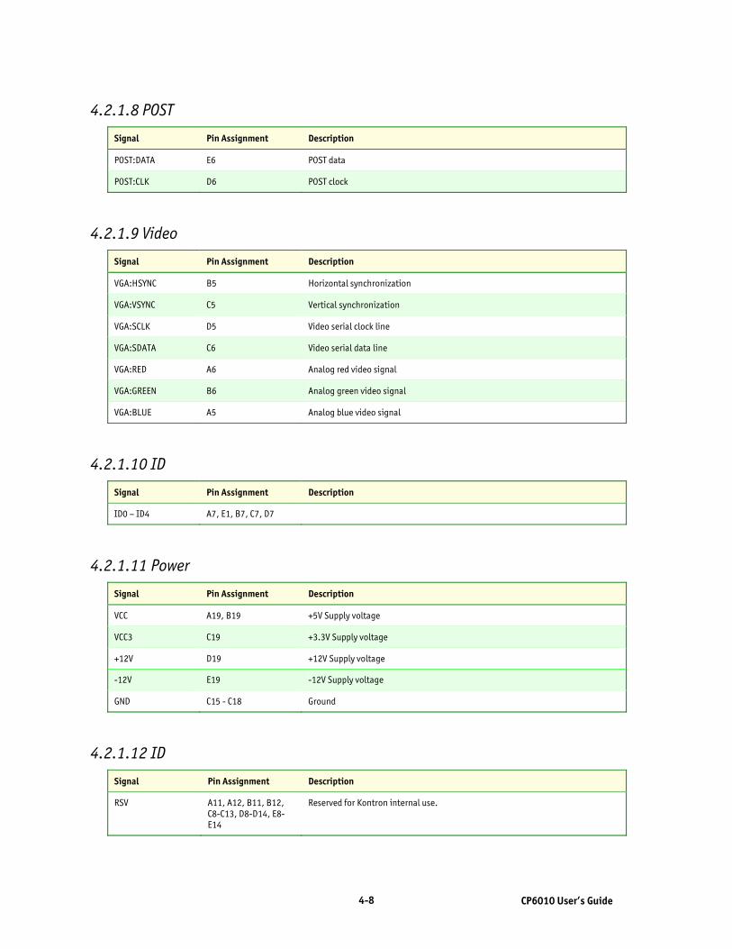
4-8 CP6010 User’s Guide
4.2.1.8 POST
Signal Pin Assignment Description
POST:DATA E6 POST data
POST:CLK D6 POST clock
4.2.1.9 Video
Signal Pin Assignment Description
VGA:HSYNC B5 Horizontal synchronization
VGA:VSYNC C5 Vertical synchronization
VGA:SCLK D5 Video serial clock line
VGA:SDATA C6 Video serial data line
VGA:RED A6 Analog red video signal
VGA:GREEN B6 Analog green video signal
VGA:BLUE A5 Analog blue video signal
4.2.1.10 ID
Signal Pin Assignment Description
ID0 – ID4 A7, E1, B7, C7, D7
4.2.1.11 Power
Signal Pin Assignment Description
VCC A19, B19 +5V Supply voltage
VCC3 C19 +3.3V Supply voltage
+12V D19 +12V Supply voltage
-12V E19 -12V Supply voltage
GND C15 - C18 Ground
4.2.1.12 ID
Signal Pin Assignment Description
RSV A11, A12, B11, B12, C8-C13, D8-D14, E8-E14
Reserved for Kontron internal use.

4-9 CP6010 User’s Guide
4.2.2 J4 Signal Specification
4.2.2.1 SCSI Interface
Signal Pin Assignment Description
D0+ to D15+ D4, A5, D5, A7, D7, A8, D8, A10, A24, D24, D22, D25, A1, D1, A2, D2
D0- to D15- E4, B5, E5, B7, E7, B8, E8, B10, B24, E24, B25, E25, B1, E1, B2, E2
SCSI data.
The SCSI data lines drive the ID during arbitration and selection, and command and data information as well as status and messages.
TERMPWR1 to TERMPWR9
A16,B16, A15, B15, D15, E15, B11, D11, E11
Termination power.
IO +/- D22, E22 In/Out – Indicates the in direction when asserted and the out direction when not asserted.
REQ + / - A22, B22 Request – A target will assert REQ to indicate a byte is ready or is needed by the target.
CD + / - D21, E21 Command/Data – Indicates Command or message phase when asserted, and data phase when not asserted.
SEL + / - A21, B21 SCSI Select – The line is driven after a successful arbitration to select as an initiator or reselect as a target and otherwise it is received.
MSG + / - D19, E19 SCSI Message - Indicates a message phase when asserted, and command or data phase when not asserted.
RST + / - A19, B19 Reset – Signal is interpreted as a hard reset and will clear all commands pending on the SCSI bus.
ACK +/- D18, E18 Acknowledge – Indicates a byte is ready for or was received from the target.
BSY + / - A18, B18 Busy – Handshake signal used during arbitration.
ATN + / - D16, E16 Attention – This line is activated when a special condition occurs.
DPL + / - D10, E10 SCSI High Parity – Provide odd parity for data lines
DPH + / - A4, B4 SCSI Low Parity – Provide odd parity for data lines.
DIFFSENS A11
Differential Sense
Detects the voltage level of a SCSI signal to determine whether it is a single-ended or LVD.
VCC B23 +5V
VCC3 E23 +3.3V
GND A3, A6, A9, A17, A20, B3, B6, B9, B17, B20, C1 to C25, D3,D6,D9, D17, D20, E3, E6,E9, E17, E20
Ground
RSV A23, D23 Reserved for Kontron internal use.

4-10 CP6010 User’s Guide
4.2.2.2 PIM Interface
Signal Pin Assignment Description
PIM1 to PIM 10 A25, D25, B25, E25, A24,D24, B24, E24, A22, D22
PIM11 to PIM20 B22, E22, A21, D21, B21, E21, A19, D19, B19, E19
PIM21 to PIM30 A18, D18, B18, E18, A16, D16, B16, E16, A15, D15
PIM31 to PIM40 B15, E15, A11, D11, B11, E11, A10,D10, B10, E10
PIM41 to PIM50 A8, D8, B8, E8, A7,D7, B7, E7, A5, D5
PIM51 to PIM60 B5, E5, A4, D4, B4, E4, A2, D2, B2, E2
PIM61 to PIM64 A1, D1, B1, E1
PIM Interface
VCC B23 +5V
VCC3 E23 +3.3V
GND A3, A6, A9, A17, A20, B3, B6, B9, B17, B20, C1 to C25, D3,D6,D9, D17, D20, E3, E6,E9, E17, E20
Ground
4.2.2.3 Mezzanine Connector (JN4)
Signal Pin Assignment Description
P1+ to P32+ 1, 2, 5, 6, 9, 10, 13, 14, 17, 18, 21, 22, 25, 26, 29, 30, 33, 34, 37, 38, 41, 42, 45, 46, 49, 50, 53, 54, 57, 58, 61, 62
P1- to P32- 3, 4, 7, 8, 11, 12, 15, 16, 19, 20, 23, 24, 27, 28, 31, 32, 35, 36, 39, 40, 43, 44, 47, 48, 51, 52, 55, 56, 59, 60, 63, 64

4-11 CP6010 User’s Guide
4.2.3 J5 Signal Specification
4.2.3.1 IDE Interface
Signal Pin Assignment Description
IDE:RESET# E15 Reset signal
IDE1:D0-D15 A18, D18, A17, D17, A16, D16, A15, D15, B15, E16, B16, E17, B17, E18, B18, E19,
Disk Data – These signals are used to transfer data to or from the IDE device.
IDE1:DMARQ D19 Disk DMA Request - This signal is directly driven from the IDE device DMARQ signal. It is asserted by the IDE device to request a data transfer.
IDE1:IOW# B19 Disk I/O Write – In normal IDE mode, this is the command to the IDE device that it may latch data from data lines.
IDE1:IOR# A19 Disk I/O Read – In normal IDE mode, this is the command to the IDE device that it may drive data on SDD lines.
IDE1:IORDY E20
I/O Channel Ready –This input signal is negated to extend the host transfer cycle of any host register read/write access when the drive is not ready to respond to a data transfer request. When not negated, it is in a high impedance state.
IDE1:DMACK# D20
DMA Acknowledge – This signal directly drives the IDE device /DMACK signal. It is asserted to indicate to IDE DMA slave devices that a given data transfer cycle is a DMA data transfer cycle.
IDE1:ACT# A22 Activity indicator
IDE1:IRQ B20 IRQ line
IDE1:IOCS16# A20 I/O Chip Select - Indicates to the host that the 16-bit data port has been addressed and the drive is prepared to send/receive a 16-bit data word.
IDE1:A0 – A2 B21, D21, A21 Disk Address – These signals indicates which byte in either the ATA command block or control block is being addressed.
IDE1:CS0#, CS1# D22, B22 Chip Select - For ATA control register
IDE1:PDIAG# E21
Diagnostic - Will be asserted by Drive 1 to indicate to Drive 0 that it has passed diagnostics. Following a power-on reset or software reset, Drive 1 will negate -PDIAG within 1 msec to indicate to Drive 0 that it is busy.
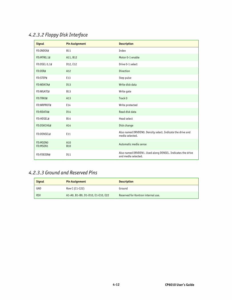
4-12 CP6010 User’s Guide
4.2.3.2 Floppy Disk Interface
Signal Pin Assignment Description
FD:INDEX# B11 Index
FD:MTR0,1# A11, B12 Motor 0-1 enable
FD:DSEL 0,1# D12, E12 Drive 0-1 select
FD:DIR# A12 Direction
FD:STEP# E13 Step pulse
FD:WDATA# D13 Write disk data
FD:WGATE# B13 Write gate
FD:TRK0# A13 Track 0
FD:WRPROT# E14 Write protected
FD:RDATA# D14 Read disk data
FD:HDSEL# B14 Head select
FD:DSKCHG# A14 Disk change
FD:DENSEL# E11 Also named DRVDEN0. Density select. Indicate the drive and media selected.
FD:MSEN0 FD:MSEN1
A10 B10
Automatic media sense
FD:FDEDIN# D11 Also named DRVDEN1. Used along DENSEL. Indicates the drive and media selected.
4.2.3.3 Ground and Reserved Pins
Signal Pin Assignment Description
GND Row C (C1-C22) Ground
RSV A1-A9, B1-B9, D1-D10, E1-E10, E22 Reserved for Kontron internal use.
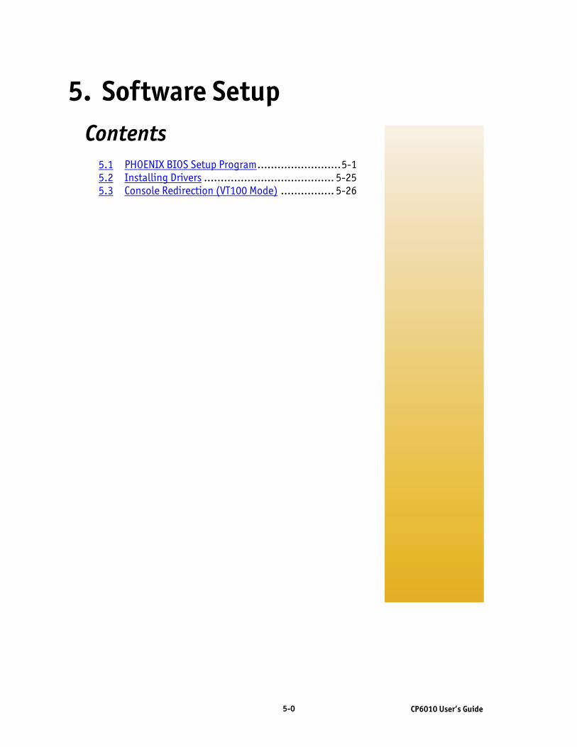
5-0 CP6010 User’s Guide
5. Software Setup Contents
5.1 PHOENIX BIOS Setup Program.........................5-1 5.2 Installing Drivers ....................................... 5-25 5.3 Console Redirection (VT100 Mode) ................ 5-26

5-1 CP6010 User’s Guide
5.1 PHOENIX BIOS Setup Program All relevant information for operating the board and connecting peripherals is stored in the CMOS memory. A battery-backed up memory holds this information when the board is powered off; the BIOS setup program is required to make changes to the setup.
5.1.1 Accessing the BIOS Setup Program The system Basic Input Output System (BIOS) provides an interface between the operating system and the hardware of the CP6010 processor board. The CP6010 uses the Phoenix Setup program, a setup utility in flash memory that is accessed by pressing the <DELETE> key at the appropriate time during system boot. This utility is used to set configuration data in CMOS RAM.
CAUTION
Before modifying CMOS setup parameters, ensure that the W19 battery selection jumper is installed to enable the CMOS battery back up. (See Section 3.)
To run the Phoenix Setup program incorporated in the ROM BIOS:
1. Turn on or reboot the system. 2. When you get the following message, hit <DELETE> key to enter SETUP.
Phoenix ServerBIOS 3 Release 6.0
Copyright 1985-2001 Phoenix Technologies Ltd.
All Rights Reserved
KONTRON CP6010 BIOS Version 3.1

5-2 CP6010 User’s Guide
The main menu of the Phoenix BIOS CMOS Setup Utility appears on the screen.
KONTRON CP6010 BIOS Version 3.1
Main Advanced Monitoring Boot Exit
Item Specific Help
System Time [13:30:00] System Date [01/01/2002]
Legacy Diskette A [1.44/1.25 MB
Additional IDE Reset Delay [75]
► Primary Master [None] ► Primary Slave [None]
► Secondary Master [None]
► Secondary Slave [None]
POST Errors [Enabled]
System Memory 640 KB
Extended Memory 262080 KB
<Tab>, <Shift-Tab>, or
<Enter> selects field.
F1 Help Select Item +/- Change Values F9 Setup Defaults
Esc Exit Select Menu Enter Select ► submenu F10 Save and Exit
Whenever you are not sure about a setting, refer to the list of default values. The list is provided in the event that a value has been changed and you wish to set this option to its original value. Loading the SETUP defaults affects all parameters and will reset options previously altered. The Setup Defaults values provide optimum performance settings for all devices and system features.
Note: The CMOS setup option is based on BIOS Version 3.1. The options and default settings can change in a new BIOS release.
CAUTION
These parameters have been provided to give control over the system. However, the values for these options should be changed only if the user has a full understanding of the timing relationships involved.
Main

5-3 CP6010 User’s Guide
5.1.2 Menu Bar The Menu Bar at the top of the window lists these selections:
Menu Selection Description
Main Use this menu for basic system configuration. Advanced Use this menu to set the Advanced Features available on your system. Monitoring Use this menu to configure Monitoring features. Boot Use this menu to determine the booting device order. Exit Use this menu to exit the BIOS.
Use the left and right and arrows keys to make a selection.
5.1.2.1 Legend Bar
Use the keys listed in the legend bar on the bottom to make your selections or exit the current menu. The chart on the following page describes the legend keys and their alternates.
Key Function
<F1> or <Alt-H> General Help windows (See 4.1.2.2).
<Esc> Exit this menu.
arrow keys Select a different menu.
<Home> or <End> Move cursor to top or bottom of window.
<PgUp> or <PgDn> Move cursor to top or bottom of window.
<F5> or <-> Select the Previous Value for the field.
<F6> or <+> or <Space> Select the Next Value for the field.
<F9> Load the Default Configuration values for all menus
<F10> Save and exit.
<Enter> Execute Command; display possible value for this field or select the submenu.
To select an item, use the arrow keys to move the cursor to the field your want. Then use the plus-and-minus value keys to select a value for that field. To save values commands in the Exit Menu save the values currently displayed in all the menus. To display a submenu, use the arrow keys to move the cursor to the submenu your want. Then press <Enter>. A pointer (�) marks all submenus.
5.1.2.2 Field Help Window
The help window on the right side of each menu displays the help text for the currently selected field. It updates as you move the cursor to each field.
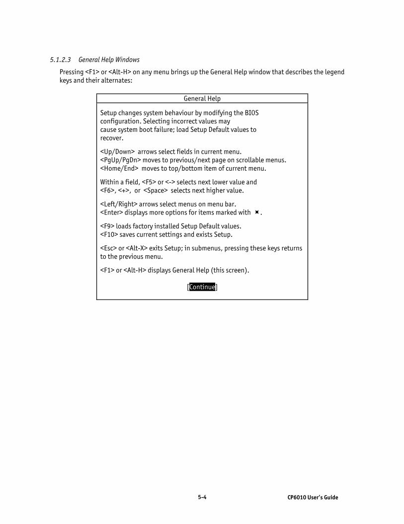
5-4 CP6010 User’s Guide
5.1.2.3 General Help Windows
Pressing <F1> or <Alt-H> on any menu brings up the General Help window that describes the legend keys and their alternates:
General Help
Setup changes system behaviour by modifying the BIOS configuration. Selecting incorrect values may cause system boot failure; load Setup Default values to recover.
<Up/Down> arrows select fields in current menu. <PgUp/PgDn> moves to previous/next page on scrollable menus. <Home/End> moves to top/bottom item of current menu.
Within a field, <F5> or <-> selects next lower value and <F6>, <+>, or <Space> selects next higher value.
<Left/Right> arrows select menus on menu bar. <Enter> displays more options for items marked with .
<F9> loads factory installed Setup Default values. <F10> saves current settings and exists Setup.
<Esc> or <Alt-X> exits Setup; in submenus, pressing these keys returns to the previous menu.
<F1> or <Alt-H> displays General Help (this screen).
[Continue]

5-5 CP6010 User’s Guide
5.1.2.4 Main Menu Selection
The scroll bar on the right of any windows indicates that there is more than one page of information in the windows. Use <PgUp> and <PgDn> to display all the pages. Pressing <Home> and <End> displays the first and last page. You can make the following selections on the Main Menu itself. Use the submenus for other selections.
Feature Options Description
System Time HH:MM:SS Set the system time.
System Date MM/DD/YYYY Set the system date.
Legacy Diskette A:
Disabled 720 Kb 3 1/2” 1.44/1. 25 MB 3 1/2” 2.88 MB 3 ½
Select the type of floppy disk drive installed in your system.
Note : 1.25MB 3 1/2” references a 1024 byte/sector Japanese media format.
The 1.25MB, 3 1/2 diskette requires a 3-Mode floppy-disk drive.
Additional IDE Reset Delay
0 to 255 ms Additional Delay after IDE soft reset for auto-detect the drives.
None None : No booting device installed.
CD-ROM
Multi-Sector Transfers LBA Mode Control 32 BIT I/O Transfer Mode Ultra DMA Mode
Multi-Sector Transfers Choices : Disabled, 2,4,8, and 16 sectors Any selection except Disabled determines the number of sectors transferred per block. Standard is 16 sectors per block. LBA Mode Control Choices : Disabled, Enabled Enabling LBA causes Logical Block Addressing to be used in place of Cylinders, heads, and Sectors. 32 Bit I/O Choices : Disabled, Enabled Enables 32-bit communication between CPU and IDE card. Requires PCI or local bus. Transfer Mode
Choices : Standard, Fast PIO 1, Fast PIO 2, Fast PIO 3, Fast PIO 4, FPI0 3 / DMA 1, FPIO 4 / DMA2.
Selects the method for transferring the data between the hard disk and system memory. The Setup menu only lists those options supported by the drive and platform. Ultra DMA Mode Choices : Disabled, Mode 0, 1, 2, 3, 4, 5. Select the Ultra DMA mode used for moving data to/from the drive. Autotype the drive to select the optimum transfer mode. IDE SMART Monitoring Choices: Enable/Disable
Primary Master Type
ATAPI Removable Same choices as CD-ROM

5-6 CP6010 User’s Guide
Main Menu Selection (continued)
Feature Options Description
IDE Removable Same choices as CD-ROM Other ATAPI Same choices as CD-ROM
Primary Master
(Continued)
Type (continu
ed (USER)
Cylinders Heads Sectors Maximum Capacity Multi-Sector Transfers LBA mode Control 32 Bit I/O Transfer Mode Ultra DMA Mode
Cylinders Set the number of cylinders Heads Set the number of heads. Choices are 1 to 16 Sectors Set the number of sectors per track Maximum Capacity Maximum capacity is displayed according to the cylinders, heads and sectors selected. Multi-Sector Transfers Choices are : Disabled, 2, 4, 8 and 16 sectors. Specify the number of sectors per block for multiple sector transfers. “MAX” refers to the size the disk returns when queried. LBA Mode Control Choices are : Enabled, Disabled Enabling LBA cause Logical Block Addressing to be used in place of Cylinders Heads and Sectors 32 Bit I/O Choices are : Enabled, Disabled. This setting enables or disables 32 bit IDE data transfers. Transfer Mode Choices are : Standard, Fast PIO 1, Fast PIO 2, Fast PIO 3, Fast PIO 4, FPI0 3 / DMA 1, FPIO 4 / DMA2. Select the method for moving data to/from the drive. Autotype the drive to select the optimum transfer mode. Ultra DMA Mode Choices are: Disabled, Mode 0 to 5. Select the Ultra DMA mode used for moving data to/from the drive Autotype the drive to select the optimum transfer mode.
Auto BIOS autodetects the hard disk installed
Primary Slave
Same as Primary Master
Secondary Master Same as Primary Master
Secondary Slave Same as Primary Master
POST Errors Enabled Disabled
Pauses and displays SETUP entry or resumes boot prompt if error occurs on boot. If disabled, system always attempts to boot.
System Memory N/A
Displays amount of conventional memory detected during boot up.
Extended Memory N/A
Displays the amount of RAM memory detected during boot up minus the base memory (1 MB).

5-7 CP6010 User’s Guide
5.1.2.5 Advanced Menu Selection
You can make the following selections on the Advanced Menu. Use the submenus for other selections.
Feature Options Description
Boot Settings Configuration
This is a submenu; see section 5.1.2.5.1 Additional setup menus to configure boot settings
PCI Configuration
This is a submenu; see section 5.1.2.5.2 Additional setup menus to configure PCI devices
On-Board Device Configuration
This is a submenu; see section 5.1.2.5.3
Peripheral Configuration
Advanced Chipset Control
This is a submenu; see section5.1.2.5.4
Console Redirection
This is a submenu; see section 5.1.2.5.5
Additional setup menus to configure console.
Advanced Processor Options
This is a submenu; see section 5.1.2.5.6

5-8 CP6010 User’s Guide
5.1.2.5.1 Boot Settings Configuration You can make the following selections on the Boot Settings Configuration submenu. Use the submenus for other selections.
Feature Options Description
Installed O/S
Other Win95 Win98 WinMe Win2000
Other : General Settings
Win95/Win98/WinMe/Win2000: Specific Settings
Note : An incorrect setting can cause some operating systems to display unexpected behaviour.
Enable ACPI Yes No
Enable/Disable ACPI BIOS (Advance Configuration and Power Interface)
Remap Memory above 4GB
DIMM Remapping Chipset Remapping Disabled
The default option in the BIOS is set to DIMM remapping. DIMM remapping under nearly all cases will give less memory in a 4GB system than Chipset Remapping. Chipset Remapping is also faster, having scored a memory bandwidth of 3078 MB/s vs 2830 MB/s for DIMM remapping (benchmark was done with Sisoftware Sandra 2005 under Windows 2003 Server in PAE mode). The DIMM Remapping feature was done to allow CPU MTRRs to be set for PCI bursting. When doing Chipset Remapping or no remapping, and there >= 4GB, the MTRR are set so that an Uncacheable region is set over all PCI memory up to 4GB. When a range is declared uncacheable, it can't be changed to improve performance (PCI bursting).
Reset Configuration Data
No Yes
Select “Yes” if you want to clear the Extended System Configuration Data (ESCD) area.
Boot-time Diagnostic Screen
Enabled Disabled
Displays the Diagnostic Screen during boot.
Always enabled when console redirection is activated.
Extended RAM Test Step
Every Location First KB First 64 KB
Select how to perform extended memory tests. First KB : Test First KB of each MB. First 64 KB : Test First 64 KB of each MB.
Summary Screen Delay
None 5 seconds
Delay to display the system configuration at boot time.
Save CMOS in FLASH
Disabled Enabled
Saving CMOS memory content into Flash Memory will prevent losing CMOS options when battery fails.
Retry Boot Sequence
Disabled
Enabled
Enable this option to Retry the Boot sequence until a successful boot (infinite retry).
PS/2 Mouse Disable Enabled
‘Disabled’ prevents installed PS/2 mouse from functioning but frees up IRQ 12. ‘Enabled’ forces PS/2 mouse port to be enabled regardless if a mouse is present.
Multiprocessor Specification
1.1 1.4
Configures the multiprocessor specification (MPS) revision level. Some operating systems will require revision 1.1 for compatibility.
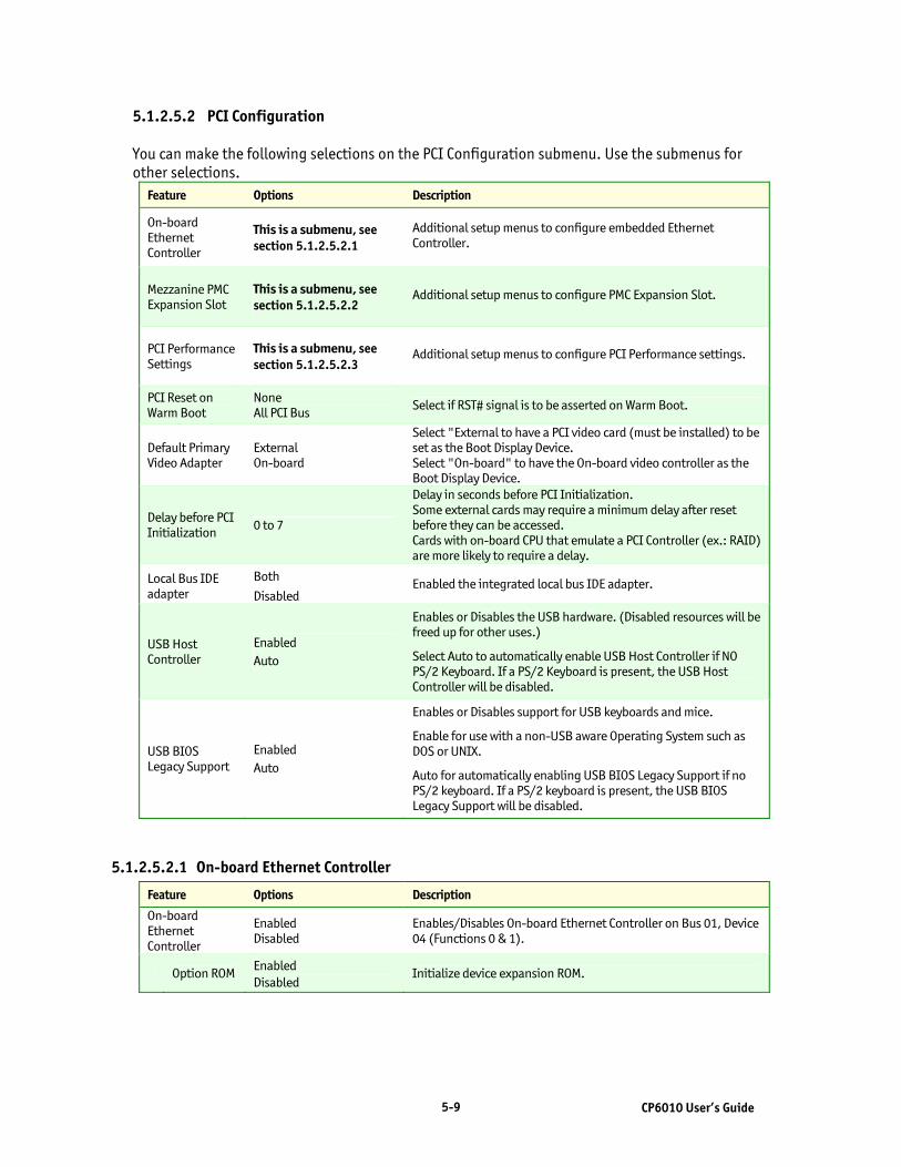
5-9 CP6010 User’s Guide
5.1.2.5.2 PCI Configuration You can make the following selections on the PCI Configuration submenu. Use the submenus for other selections.
Feature Options Description
On-board Ethernet Controller
This is a submenu, see section 5.1.2.5.2.1
Additional setup menus to configure embedded Ethernet Controller.
Mezzanine PMC Expansion Slot
This is a submenu, see section 5.1.2.5.2.2
Additional setup menus to configure PMC Expansion Slot.
PCI Performance Settings
This is a submenu, see section 5.1.2.5.2.3
Additional setup menus to configure PCI Performance settings.
PCI Reset on Warm Boot
None All PCI Bus
Select if RST# signal is to be asserted on Warm Boot.
Default Primary Video Adapter
External On-board
Select "External to have a PCI video card (must be installed) to be set as the Boot Display Device. Select "On-board" to have the On-board video controller as the Boot Display Device.
Delay before PCI Initialization 0 to 7
Delay in seconds before PCI Initialization. Some external cards may require a minimum delay after reset before they can be accessed. Cards with on-board CPU that emulate a PCI Controller (ex.: RAID) are more likely to require a delay.
Local Bus IDE adapter
Both
Disabled Enabled the integrated local bus IDE adapter.
USB Host Controller
Enabled Auto
Enables or Disables the USB hardware. (Disabled resources will be freed up for other uses.)
Select Auto to automatically enable USB Host Controller if NO PS/2 Keyboard. If a PS/2 Keyboard is present, the USB Host Controller will be disabled.
USB BIOS Legacy Support
Enabled Auto
Enables or Disables support for USB keyboards and mice.
Enable for use with a non-USB aware Operating System such as DOS or UNIX.
Auto for automatically enabling USB BIOS Legacy Support if no PS/2 keyboard. If a PS/2 keyboard is present, the USB BIOS Legacy Support will be disabled.
5.1.2.5.2.1 On-board Ethernet Controller
Feature Options Description
On-board Ethernet Controller
Enabled Disabled
Enables/Disables On-board Ethernet Controller on Bus 01, Device 04 (Functions 0 & 1).
Option ROM Enabled Disabled
Initialize device expansion ROM.

5-10 CP6010 User’s Guide
5.1.2.5.2.2 Mezzanine PMC Expansion Slot
Feature Options Description
Option ROM Enabled Disabled
Initialize device expansion ROM.
Enable Master
Enabled Disabled
Enable selected device as a PCI bus master.
Latency Timer
Default, 0020h, 0040h, 0060h, 0080h, 00A0h, 00C0h or 00E0h
Minimum guaranteed time slice allotted for bus master in units of PCI bus clocks.
5.1.2.5.2.3 PCI Performance Settings
Feature Options Description
PCI Cache Line Size
0, 1, 2, 4, 8 or 16 DWORDS
Set the Cache Line Size in DWORDS.
Sets the Cache Line Size Register in the Configuration Space of PCI devices.
On-board PCI-PCI Bridge settings:
Following options control the behaviour of the On-board PCI-X bridge. The Bridge has an EEPROM to initialize the registers. If it’s content is valid, the options will be shown in grey and are not available for change.
Force 64-bit Control
Disabled Both Secondary Primary
32-bit Prefetchable reads or 32-bit Posted Memory Write cycles on one side will be converted to 64-bit cycles on completion to target side if target supports 64-bit transfers.
Smart Prefetch Mechanism
Enabled Disabled
After a prefetch command, the remaining prefetched data will NOT be discarded, but will be available for the next Read Command with consecutive address.
Smart Prefetch Timeout
32, 64, 128 or 256 PCICLK When Smart Prefetch is Enabled, the prefetched data is only discarded upon a Timeout.
Prefetching scheme
‘By EEPROM’ Aggressive Normal Manual
Controls Secondary PCI bus Prefetch behaviour (no effect when in PCI-X mode).
If set to ‘By EEPROM’, the values shown are taken from the Bridge and are not available for change. This happens if a valid EEPROM content is detected and were loaded by the Bridge.
The default aggressive Prefetching may affect the overall performance with some PCI Masters that cannot prefetch a lot of data due to limited buffers size or other reasons.
If set to ‘Manual’, the options can be changed for optimum performance, which depends on the PCI device(s) present.
PCI Primary Initial Prefetch count
‘= PCI CLS’, 2, 4, 8 or 16 Dwords
Controls initial Prefetch Cache Lines count on the Primary bus during reads to prefetchable memory space.
Uses size defined in "PCI Cache Line Size" when setting is set to
'= PCI CLS'.
PCI Sec. Initial Prefetch count
8, 16 or 32 Dwords Controls initial Prefetch Dwords count on the Secondary bus during reads initiated from the primary port (no effect when in PCI-X mode).

5-11 CP6010 User’s Guide
PCI Sec. Incremental Prefetch count
None, 4, 8, 12, 16, 20, 24, 28 or 32 Dwords
Controls Incremental Read Prefetch Dwords count. When an entry's remaining Prefetch Dword count falls below this value, the bridge will prefetch an additional "PCI Sec. Incremental Prefetch count" Dwords (no effect when in PCI-X mode).
The count must not exceed half the value in the "PCI Sec. Maximum Prefetch count". Otherwise, no Incremental Prefetch will be performed.
PCI Sec. Maximum Prefetch count
2 to 64 Dwords
Controls the maximum count of prefetcheable Dwords that are allocated to one entry on the Secondary when flow through for that entry was not achieved (no effect when in PCI-X mode).
Exception: 0 = 256 bytes (64 Dwords) = maximum programmable count.
On-board Bridge Enable P_SERR# event
Enabled Disabled
When enabled if read to secondary bus fail, P_SERR will be asserted. NOTE: Available only with board revision 2.
5.1.2.5.3 On-board Device Configuration You can make the following selections on the On-board Device Configuration submenu.
Feature Options Description
Serial port A Enabled Disabled Auto
Configure Serial Port A using options: Disabled : No configuration Enabled : User configuration Auto : BIOS or OS chooses configuration
Base I/O address
3F8/IRQ4, 2F8/IRQ3, 3E8/IRQ4 or 2E8/IRQ3
Sets the base I/O address for Serial Port A.
Serial port B
Enabled Disabled Auto
Configure Serial Port B using options: Disabled : No configuration Enabled : User configuration Auto : BIOS or OS chooses configuration
Mode RS-422 RS-485 RS-232
Set the mode for Serial Port B.
Base I/O address
3F8/IRQ4, 2F8/IRQ3, 3E8/IRQ4 or 2E8/IRQ3
Sets the base I/O address for Serial Port B.
Floppy Disk Controller
Enabled Disabled
Configure the floppy disk controller.
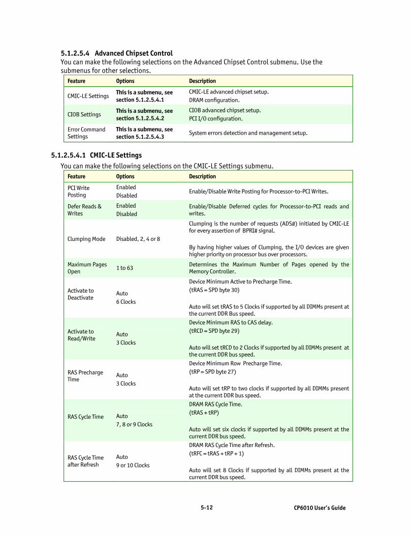
5-12 CP6010 User’s Guide
5.1.2.5.4 Advanced Chipset Control You can make the following selections on the Advanced Chipset Control submenu. Use the submenus for other selections.
Feature Options Description
CMIC-LE Settings This is a submenu, see section 5.1.2.5.4.1
CMIC-LE advanced chipset setup. DRAM configuration.
CIOB Settings This is a submenu, see section 5.1.2.5.4.2
CIOB advanced chipset setup. PCI I/O configuration.
Error Command Settings
This is a submenu, see section 5.1.2.5.4.3
System errors detection and management setup.
5.1.2.5.4.1 CMIC-LE Settings You can make the following selections on the CMIC-LE Settings submenu.
Feature Options Description
PCI Write Posting
Enabled Disabled
Enable/Disable Write Posting for Processor-to-PCI Writes.
Defer Reads & Writes
Enabled Disabled
Enable/Disable Deferred cycles for Processor-to-PCI reads and writes.
Clumping Mode Disabled, 2, 4 or 8
Clumping is the number of requests (ADS#) initiated by CMIC-LE for every assertion of BPRI# signal. By having higher values of Clumping, the I/O devices are given higher priority on processor bus over processors.
Maximum Pages Open
1 to 63 Determines the Maximum Number of Pages opened by the Memory Controller.
Activate to Deactivate
Auto 6 Clocks
Device Minimum Active to Precharge Time. (tRAS = SPD byte 30) Auto will set tRAS to 5 Clocks if supported by all DIMMs present at the current DDR Bus speed.
Activate to Read/Write
Auto 3 Clocks
Device Minimum RAS to CAS delay. (tRCD = SPD byte 29) Auto will set tRCD to 2 Clocks if supported by all DIMMs present at the current DDR bus speed.
RAS Precharge Time
Auto 3 Clocks
Device Minimum Row Precharge Time. (tRP = SPD byte 27) Auto will set tRP to two clocks if supported by all DIMMs present at the current DDR bus speed.
RAS Cycle Time
Auto 7, 8 or 9 Clocks
DRAM RAS Cycle Time. (tRAS + tRP) Auto will set six clocks if supported by all DIMMs present at the current DDR bus speed.
RAS Cycle Time after Refresh
Auto 9 or 10 Clocks
DRAM RAS Cycle Time after Refresh. (tRFC = tRAS + tRP + 1) Auto will set 8 Clocks if supported by all DIMMs present at the current DDR bus speed.

5-13 CP6010 User’s Guide
5.1.2.5.4.2 CIOB Settings You can make the following selections on the CIOB Settings submenu.
Feature Options Description
Memory Read Byte Count
512, 1K, 2K or 4K Bytes
Sets the maximum byte count the device uses when initiating a sequence with one of the Burst Memory Read Commands. CIOB Function 0: On-board LAN and PCIX-to-PCIX Bridge.
Memory Read Byte Count
512, 1K, 2K or 4K Bytes
Sets the maximum Byte Count the Device uses when initiating a sequence with one of the Burst Memory Read Commands. CIOB Function 2: Bridge/PMC Mezzanine.
Stray Read to Stream
Enabled Disabled
When Enabled, conventional PCI Mode Memory Read Commands (Stray commands) are treated as Stream Commands (Memory Read Multiple, Memory Read Line Commands). The I/O Cache uses the stream prefetching algorithms for these commands.
IMB Transmit Arbiter Slots
1 or 2 Select how many slots the IMB Transmit Arbiter will allocate for Primary PCI Bus Commands in, per arbitration window.
Buffer Manager Dual Request
Enabled Disabled
If Enabled, the Buffer Manager generates two, 128-byte requests per arbitration window. If disabled, the buffer manager generates one 128-byte request per arbitration window.
5.1.2.5.4.3 Error Command Settings You can make the following selections on the Error Command Settings submenu.
Feature Options Description
ECC Config Enabled Disabled
If all memory in the system supports ECC, then use this option to enable or disable ECC support.
ECC Threshold Disabled, 4, 8, 16, 32, 64, 128 or 254
The limit number of ECCs allowed by CMIC for each row before it asserts ALERT#. When the threshold is reached, the ALERT# is used to log into the DMI log the number of ECC errors detected for each rows of DRAM.
Scrubbing Enabled Disabled
When Enabled, CMIC-LE writes back the ECC corrected Memory Data back to the DRAM.
Action after Uncorrectable ECC
Continue, Halt or Reboot
Select what the system will do when an uncorrectable ECC error has been detected. Continue – Log the error (if not fatal to the system) into the DMI log and try to resume process. Halt – Log the error (if not fatal to the system) into the DMI log and halt. The system will appear stuck and must be reset. Reboot – Log the error (if not fatal to the system) into the DMI log and do a PCI reset to restart the system.
IMBus Error Enabled Disabled
Select "Enabled' to allow logging of IMBus Error events. The CMIC-LE and CIOB are interfaced with a high speed Inter Module Bus (IMB).
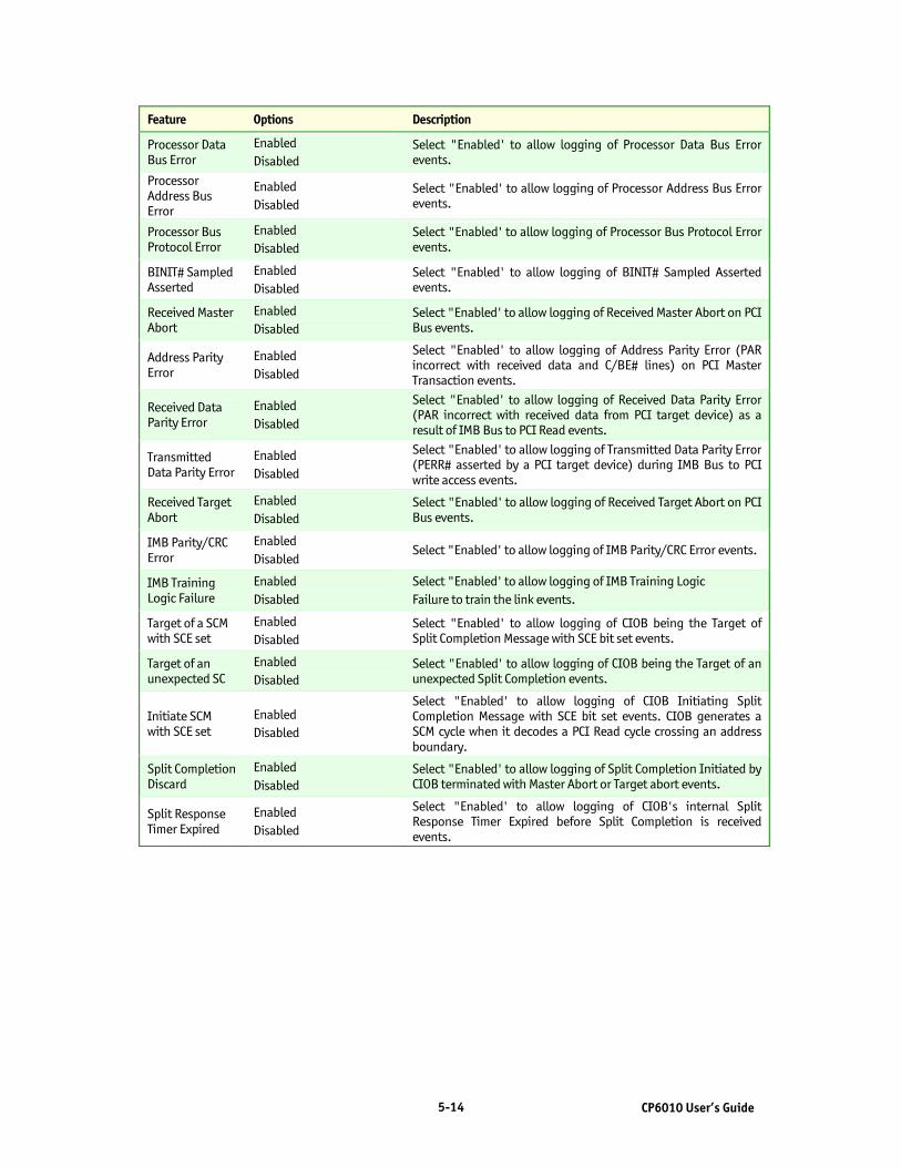
5-14 CP6010 User’s Guide
Feature Options Description
Processor Data Bus Error
Enabled Disabled
Select "Enabled' to allow logging of Processor Data Bus Error events.
Processor Address Bus Error
Enabled Disabled
Select "Enabled' to allow logging of Processor Address Bus Error events.
Processor Bus Protocol Error
Enabled Disabled
Select "Enabled' to allow logging of Processor Bus Protocol Error events.
BINIT# Sampled Asserted
Enabled Disabled
Select "Enabled' to allow logging of BINIT# Sampled Asserted events.
Received Master Abort
Enabled Disabled
Select "Enabled' to allow logging of Received Master Abort on PCI Bus events.
Address Parity Error
Enabled Disabled
Select "Enabled' to allow logging of Address Parity Error (PAR incorrect with received data and C/BE# lines) on PCI Master Transaction events.
Received Data Parity Error
Enabled Disabled
Select "Enabled' to allow logging of Received Data Parity Error (PAR incorrect with received data from PCI target device) as a result of IMB Bus to PCI Read events.
Transmitted Data Parity Error
Enabled Disabled
Select "Enabled' to allow logging of Transmitted Data Parity Error (PERR# asserted by a PCI target device) during IMB Bus to PCI write access events.
Received Target Abort
Enabled Disabled
Select "Enabled' to allow logging of Received Target Abort on PCI Bus events.
IMB Parity/CRC Error
Enabled Disabled
Select "Enabled' to allow logging of IMB Parity/CRC Error events.
IMB Training Logic Failure
Enabled Disabled
Select "Enabled' to allow logging of IMB Training Logic Failure to train the link events.
Target of a SCM with SCE set
Enabled Disabled
Select "Enabled' to allow logging of CIOB being the Target of Split Completion Message with SCE bit set events.
Target of an unexpected SC
Enabled Disabled
Select "Enabled' to allow logging of CIOB being the Target of an unexpected Split Completion events.
Initiate SCM with SCE set
Enabled Disabled
Select "Enabled' to allow logging of CIOB Initiating Split Completion Message with SCE bit set events. CIOB generates a SCM cycle when it decodes a PCI Read cycle crossing an address boundary.
Split Completion Discard
Enabled Disabled
Select "Enabled' to allow logging of Split Completion Initiated by CIOB terminated with Master Abort or Target abort events.
Split Response Timer Expired
Enabled Disabled
Select "Enabled' to allow logging of CIOB's internal Split Response Timer Expired before Split Completion is received events.

5-15 CP6010 User’s Guide
5.1.2.5.5 Console Redirection You can make the following selections on the Console Redirection submenu.
Feature Options Description
Console Redirection
Disabled Enabled
If enabled, console redirection works without the VT100 jumper to use the console redirection. This option is only used when jumper is not present.
Com Port Address
On-board COMA On-board COMB
If enabled, it will use a port on the motherboard.
Install the VT100 jumper to use the console redirection.
Baud Rate 300, 1200, 2400, 9600, 19.2K, 38.4K, 57.6K, 115.2K
Enables specified baud rate.
Parity None Fix setting: No Parity
Data Bits 8 Fix setting: 8 Data Bits
Stop Bit(s) 1 Fix setting: 1 Stop Bit
Console Type
VT100
VT100, 8bit
PC ANSI, 7bit
PC ANSI
Enables specified console type.
Flow Control None
XON/XOFF CTS/RTS
Enables flow control.
Console connection
Direct Via modem
Indicates whether the console is connected directly to the system or a modem is used to connect.
Continue C.R. after POST
Off, On Enables console redirection after OS has loaded.
5.1.2.5.6 Advanced Processor Options You can make the following selections on the Advanced Processor Options Menu. Use the submenus for other selections.
Feature Options Description
Cache Memory This is a submenu, see section 5.1.2.5.6.1
Determines how to configure specified block of memory.
Frequency Ratio Variable, based on the Ratios available of the installed Processor(s)
Selects the internal frequency multiplier of the CPU.
By default, the maximum ratio will be selected.
This option is hidden if the CPU ratio is fixed.
Hyper-Threading Technology
Enabled Disabled
Enabled for Windows XP and Linux 2.4.x (OS optimized for
Hyper-Threading Technology).
Disabled for other OS (OS not optimized for Hyper-Threading
Technology).
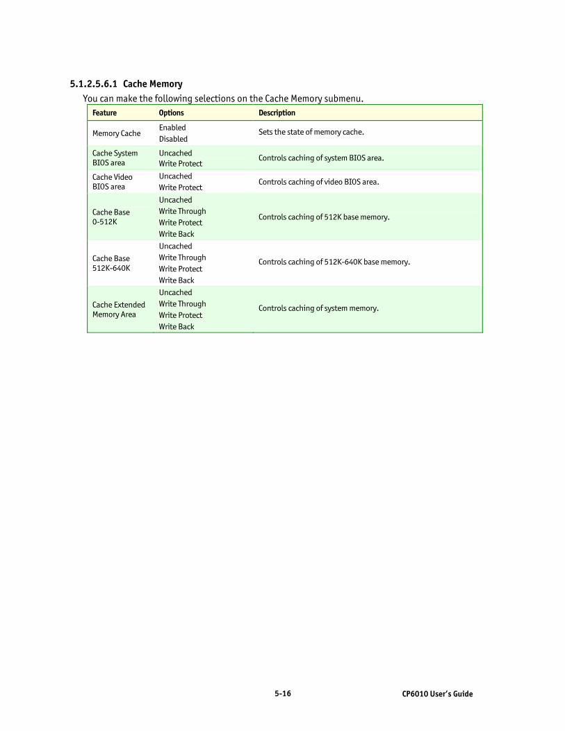
5-16 CP6010 User’s Guide
5.1.2.5.6.1 Cache Memory You can make the following selections on the Cache Memory submenu.
Feature Options Description
Memory Cache Enabled Disabled
Sets the state of memory cache.
Cache System BIOS area
Uncached Write Protect
Controls caching of system BIOS area.
Cache Video BIOS area
Uncached Write Protect
Controls caching of video BIOS area.
Cache Base 0-512K
Uncached Write Through Write Protect Write Back
Controls caching of 512K base memory.
Cache Base 512K-640K
Uncached Write Through Write Protect Write Back
Controls caching of 512K-640K base memory.
Cache Extended Memory Area
Uncached Write Through Write Protect Write Back
Controls caching of system memory.

5-17 CP6010 User’s Guide
5.1.2.6 Monitoring Menu Selection
You can make the following selections on the Monitoring Menu. Use the submenus for other selections.
Feature Options Description
Intelligent System Monitoring
This is a submenu, see section 5.1.2.6.1
DMI Event Logging
This is a submenu, see section 5.1.2.6.2
View and modify DMI event logs.
IPMI System Management OR BMC Device is not available
This is a submenu, see section 5.1.2.6.3.1
NOTE: the submenu is not available if the BMC reset jumper is installed (W5). The BIOS setup will in that case show: Check the BMC reset jumper and the IPMI Firmware version update.
Watchdog After POST
Disabled Enabled
Enables the watchdog circuit after the POST sequence. Application software must refresh the watchdog to prevent system reset.
Watchdog Duration
16 seconds 1 minute 4 minutes
Select the duration time of the watchdog timing circuitry.
Display and Clear Reset History
Enabled Disabled
Enable/disable Display FPGA Reset History in Summary Screen and Clear FPGA History.
FPGA IRQ Disabled IRQ 5 IRQ 7
Select FPGA IRQ for SWITCH, WATCHDOG and ENUM# events. If '*' is shown, this IRQ# is already used by KCS-SMS IRQ.

5-18 CP6010 User’s Guide
5.1.2.6.1 Intelligent System Monitoring You can make the following selections on the Intelligent System Monitoring submenu. Use the submenus for other selections.
Feature Options Description
Intelligent System Monitoring
Disabled Enabled
Enables/Disables the Intelligent System Monitor device. When enabled, the system will monitor some system states such as temperature and power supplies.
Interrupt Generation
Disabled
Enabled
Enables/Disables the generation of interrupts when an event occurs. This must be set to DISABLED when programs such as LANDesk® are loaded onto the system.
Beep codes for non-thermal events
Disabled
Enabled
Produces beep codes when ISM events occur for Voltages events.
One long beep plus
4 short beeps.
This alarm may not be supported by the Operating System.
Thermal Audio Alarm
Disabled
Enabled
When the Thermal Management option and this option are enabled, a continuous audible alarm is sounded when the temperature specified in the Overheat Alarm options is reached. This alarm may not be supported by the operating system.
Hardware Monitor Temperature
This is a submenu, see section 5.1.2.6.1.1
Hardware Monitor Voltage Inputs
This is a submenu, see section 5.1.2.6.1.2
Control Temperature Events
This is a submenu, see section 5.1.2.6.1.3
Control Voltage Events
This is a submenu, see section 5.1.2.6.1.4
5.1.2.6.1.1 Hardware Monitor Temperature
Feature Options Description
System board Temperature
CPU 1 Die Temperature Current Temperature
CPU 2 Die Temperature Current Temperature Hidden if only one processor is present.

5-19 CP6010 User’s Guide
5.1.2.6.1.2 Hardware Monitor Voltage Inputs
Feature Options Description
Vcore Sense CPU 1 Displays a Status and limits.
Vcore at CPU 1.
Vcore Sense CPU 2 Display a Status and limits. Hidden if only one processor present.
Vcore at CPU 1.
Vcore
Vcc3 3.3V
Vcc 5V
Vin 2.5V
Vtt
Vin 1.5V
Vbat
Vin 12V
Vin –12
Display a status and limits.
5.1.2.6.1.3 Control Temperature Events
Feature Options Description
Automatic Thermal Control Circuit
Enabled Disabled
The Thermal Control Circuit (TCC) will be activated when the processor's internal thermal sensor determines the processor is about to exceed its maximum operating temperature. When the TCC is activated, the processors clocks will be modulated (typically 30-50%).
Each processor on dual processor set-up, has it’s own TCC that can modulate the clocks separately.
CPU 1 Temperature Interrupt
Enabled Disabled
This option enables temperature events handling.
It is NOT recommended to use this feature while the Automatic Thermal Control Circuit is used.
CPU 2 Temperature Interrupt
Enabled Disabled
This option enables temperature events handling.
It is NOT recommended to use this feature while the Automatic Thermal Control Circuit is used.
Hidden if only one processor is present.
Resume Alarm (ºC) 10ºC to 70ºC with step of 4ºC
Full speed (Normal mode) will be resumed when the temperature comes down to the selected temperature.
Overheat Alarm (ºC) 30ºC to 90ºC with step of 4ºC
The CPU slows (Doze mode) when it reaches a selected temperature.
Shutdown Alarm (ºC) 60ºC to 95ºC with step of 5ºC
The CPU halts when it reaches the selected temperature. The system will have to be restarted.

5-20 CP6010 User’s Guide
5.1.2.6.1.4 Control Voltage Events Note: Any alteration done in this menu will take effect after the board is re-started.
Feature Options Description
Vcore Sense CPU 1 Voltage Int.
Enabled Disabled
This option enables voltage events handling.
Vcore Sense CPU 2 Voltage Int.
Enabled Disabled
This option enables voltage events handling.
Hidden if only one processor is present.
Vcore Voltage Interrupt Enabled Disabled
This option enables voltage events handling.
Vcc3 3.3V Voltage Interrupt
Enabled Disabled
This option enables voltage events handling.
Vcc 5V Voltage Interrupt Enabled Disabled
This option enables voltage events handling.
Vin 2.5V Voltage Interrupt Enabled Disabled
This option enables voltage events handling.
Vtt Voltage Interrupt Enabled Disabled
This option enables voltage events handling.
Vin 1.5V Voltage Interrupt Enabled Disabled
This option enables voltage events handling.
Vbat Voltage Interrupt Enabled Disabled
This option enables voltage events handling.
Vin 12V Voltage Interrupt Enabled Disabled
This option enables voltage events handling.
Vin -12 Voltage Interrupt Enabled Disabled
This option enables voltage events handling.
5.1.2.6.2 DMI Event Logging You can make the following selections on the DMI Event Logging submenu.
Feature Options Description
Event log validity
valid or Invalid Report the validity of the DMI Event log buffer (in ESCD Flash area).
Event log capacity
Space Available or Full Report the space available in the DMI event log. If set to 'Full', the event log has no more available space to store DMI events.
View DMI event log
Enter View the contents of the DMI event log.
Clear all DMI event logs
Yes/NO Setting this to yes will clear the DMI event log after rebooting.
Event Logging Enabled Disabled
Select ‘Enabled’ to allow logging of DMI events.
ECC Event Logging
Enabled Disabled
Select ‘Enabled’ to allow logging of ECC events.
Mark DMI events as read
Enter Press Enter to mark all DMI events in the event log as read.
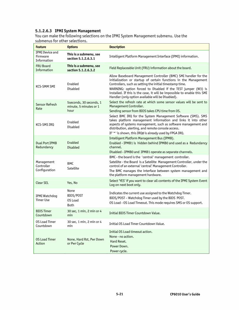
5-21 CP6010 User’s Guide
5.1.2.6.3 IPMI System Management You can make the following selections on the IPMI System Management submenu. Use the submenus for other selections. Feature Options Description
IPMI Device and Firmware Information
This is a submenu, see section 5.1.2.6.3.1
Intelligent Platform Management Interface (IPMI) information.
FRU Board Information
This is a submenu, see section 5.1.2.6.3.2
Field Replaceable Unit (FRU) information about the board.
KCS-SMM SMI Enabled Disabled
Allow Baseboard Management Controller (BMC) SMI handler for the initialization or startup of certain functions in the Management Controllers, such as setting the initial timestamp time. WARNING: option forced to Disabled if the TEST jumper (W3) is installed. If this is the case, it will be impossible to enable this SMI Handler (only option available will be Disabled).
Sensor Refresh Rate
5seconds, 30 seconds, 1 minute, 5 minutes or 1 hour
Select the refresh rate at which some sensor values will be sent to Management Controller. Sending sensor from BIOS takes CPU time from OS.
KCS-SMS IRQ Enabled Disabled
Select BMC IRQ for the System Management Software (SMS). SMS takes platform management information and links it into other aspects of systems management, such as software management and distribution, alerting, and remote console access. If '*' is shown, this IRQ# is already used by FPGA IRQ.
Dual Port IPMB Redundancy
Enabled Disabled
Intelligent Platform Management Bus (IPMB). Enabled - IPMB1 is hidden behind IPMB0 and used as a Redundancy channel. Disabled - IPMB0 and IPMB1 operate as separate channels.
Management Controller Configuration
BMC Satellite
BMC - the board is the 'central' management controller. Satellite - the Board is a Satellite Management Controller, under the control of an external ‘central’ Management Controller. The BMC manages the interface between system management and the platform management hardware.
Clear SEL Yes, No Select ‘YES’ if you want to clear all contents of the IPMI System Event Log on next boot only.
IPMI Watchdog Timer Use
None BIOS/POST OS Load Both
Indicates the current use assigned to the Watchdog Timer. BIOS/POST – Watchdog Timer used by the BIOS POST. OS Load - OS Load Timeout. This mode requires SMS or OS support.
BIOS Timer Countdown
30 sec, 1 min, 2 min or 4 min
Initial BIOS Timer Countdown Value.
OS Load Timer Countdown
30 sec, 1 min, 2 min or 4 min
Initial OS Load Timer Countdown Value.
OS Load Timer Action
None, Hard Rst, Pwr Down or Pwr Cycle
Initial OS Load timeout action. None - no action. Hard Reset. Power Down. Power cycle.
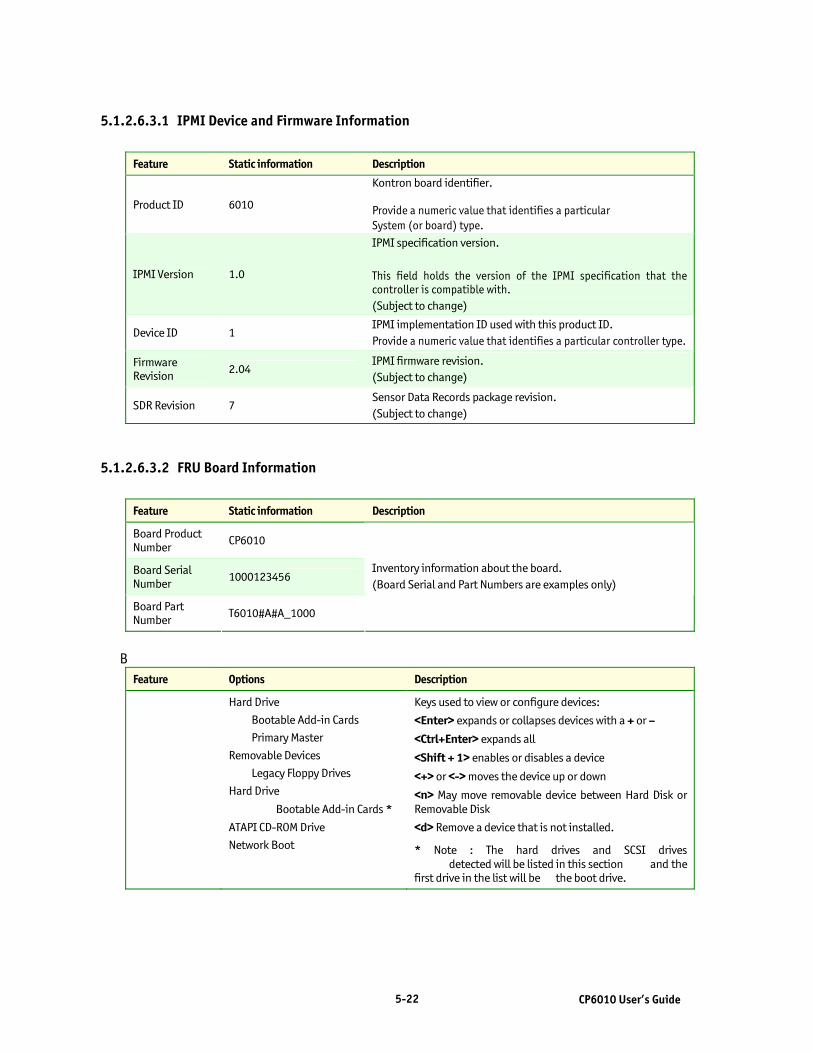
5-22 CP6010 User’s Guide
5.1.2.6.3.1 IPMI Device and Firmware Information
Feature Static information Description
Product ID 6010
Kontron board identifier. Provide a numeric value that identifies a particular System (or board) type.
IPMI Version 1.0
IPMI specification version. This field holds the version of the IPMI specification that the controller is compatible with. (Subject to change)
Device ID 1 IPMI implementation ID used with this product ID. Provide a numeric value that identifies a particular controller type.
Firmware Revision
2.04 IPMI firmware revision. (Subject to change)
SDR Revision 7 Sensor Data Records package revision. (Subject to change)
5.1.2.6.3.2 FRU Board Information
Feature Static information Description
Board Product Number
CP6010
Board Serial Number
1000123456
Board Part Number
T6010#A#A_1000
Inventory information about the board. (Board Serial and Part Numbers are examples only)
B
Feature Options Description
Hard Drive
Bootable Add-in Cards
Primary Master
Removable Devices
Legacy Floppy Drives
Hard Drive
Bootable Add-in Cards *
ATAPI CD-ROM Drive
Network Boot
Keys used to view or configure devices:
<Enter> expands or collapses devices with a + or –
<Ctrl+Enter> expands all
<Shift + 1> enables or disables a device
<+> or <-> moves the device up or down
<n> May move removable device between Hard Disk or Removable Disk
<d> Remove a device that is not installed.
* Note : The hard drives and SCSI drives detected will be listed in this section and the first drive in the list will be the boot drive.

5-23 CP6010 User’s Guide
5.1.2.7 Exit Menu Selection
Feature Options Description
Exit Saving Changes
Exit Discarding Changes
Load Setup Defaults
Discard Changes
Saves Changes
Yes / No
Yes / No
Yes / No
Yes / No
Yes / No
Exit Saving Changes Setup and save your changes to CMOS. Exit Discarding Changes Exit utility without saving Setup data to CMOS. Load Setup Defaults Exit utility without saving Setup data to CMOS. Load Setup Defaults Load default values for all SETUP items. Discard Changes Load previous values from CMOS for all SETUP items. Save Changes Save Setup Data to CMOS.
5.1.2.8 Boot Utilities Phoenix Boot Utilities are:
• Phoenix QuietBoot™
• Phoenix MultiBoot™
Phoenix QuietBoot displays a graphic illustration rather than the traditional POST messages while keeping you informed of diagnostic problems. Phoenix MultiBoot is a boot screen that displays a selection of boot devices from which you can boot your operating system.

5-24 CP6010 User’s Guide
5.1.2.9 Phoenix Quiet Boot Right after you turn on or reset the computer, Phoenix QuietBoot displays the QuietBoot Screen, a graphic illustration created by the computer manufacturer instead of the text-based POST screen, which displays a number of PC diagnostic messages. To exit the QuietBoot screen and run Setup, display the Multiboot menu, or simply display the PC diagnostic messages, you can simply press one of the hot keys described below. The QuietBoot Screen stays up until just before the operating system loads unless:
• You press <ESC> to display the POST screen.
• You press <Del> to enter Setup.
• POST issues an error message.
• The BIOS or an option ROM requests keyboard input.
The following explains each of these situations.
5.1.2.10 Press <ESC>
Pressing <ESC> switches the POST screen. The boot process continues with the text-based POST screen until the end of POST and then displays the BootFirst Menu with these options:
• Load the operating system from a boot device of your choice.
• Enter Setup.
• Exit the Boot First Menu (with <ESC>) and load the operating system from the boot devices in the order specified in Setup.
5.1.2.11 Press <Del>
Pressing < Del > at any time during POST enter Setup.
5.1.2.12 Keyboard Input Request
If the BIOS or an Option ROM (add-on card) requests keyboard input, QuietBoot switches over to the POST screen and the Option ROM displays prompts for entering the information. POST continues from there with the regular POST screen.

5-25 CP6010 User’s Guide
5.1.2.13 Phoenix Multiboot
Phoenix Multiboot expands your boot options by letting you choose your boot device, which could be a hard disk, floppy disk, CDROM, Flash Disk, SCSI or LAN. You can select your boot device in Setup, or you can choose a different device each time you boot during POST by selecting your boot device in The Boot First Menu (ESC key). Multiboot consist of :
• Setup Boot Menu
• Boot First Menu
5.2 Installing Drivers
5.2.1 Video Drivers Various drivers are provided for different operating systems and software. To install a driver, refer to the setup program located on the CD-ROM, which is provided with your board.
5.2.2 Ethernet Drivers Various drivers are provided for different operating systems and software. To install a driver, use the setup program and the ReadMe.bat file located on the CD-ROM, which is provided with your board.
5.2.3 Other Drivers For other operating system drivers and installation instructions or for more information, visit our Web site at www.kontron.com or our FTP site at ftp.kontron.ca/support/ or you may also contact Kontron Technical Support.
5-26 CP6010 User’s Guide
5.3 Console Redirection (VT100 Mode) The VT100 operating mode allows remote setup of the board. This configuration requires a remote terminal that must be connected to the board through a serial communication link.
5.3.1 Requirements The terminal should emulate a VT100 or ANSI terminal. Terminal emulation programs such as Telix© or Procom© can also be used.
5.3.2 Setup & Configuration To set up the VT100 mode:
1. Connect a monitor and a keyboard to your board and turn on the power. 2. Enter the CMOS Setup program in the “Advanced” page, “Console Redirection” menu. 3. Select the VT100 mode and the appropriate COM port and save your setup. 4. Connect the communications cable. 5. Configure your terminal to communicate using the same parameters as in the CMOS Setup. 6. Install the VT100 jumper (or use BIOS Setup; See section 5.1.2.5.5). Reboot the board. 7. Use the remote keyboard and display to setup the BIOS.
Related Jumpers: Install W4 to enable VT-100 access.
Note: If you do not require a full cable for your terminal, you can set up a partial cable by using only the TXD and RXD lines. To ignore control lines, loop them back as shown in VT100 Partial Setup cable diagram.
Save the setup, exit, and disconnect the remote computer from the board to operate in stand-alone configuration. Console Redirection is done by refreshing the video address @ B8000h at the selected baud rate. This means that a low baud rate refreshes the screen slowly, but the CPU time is maximized for applications. A high baud rate refreshes the screen rapidly but the CPU is frequently interrupted by the serial port.

5-27 CP6010 User’s Guide
Console Redirection provided by Phoenix based BIOS offers escape sequences to emulate keyboard function keys. The following table lists the escape sequences.
Escape sequence Function Escape sequence Function
Esc Del Warm Reset Esc [ 6 4 ~ (Ctrl-F1)
Esc O P F1 Esc [ 6 5 ~ (Ctrl-F2)
Esc O Q F2 Esc [ 6 6 ~ (Ctrl-F3)
Esc O R F3 Esc [ 6 7 ~ (Ctrl-F4)
Esc O S F4 Esc [ 6 8 ~ (Ctrl-F5)
Esc O w F3 Esc [ 6 9 ~ (Ctrl-F6)
Esc O x F4 Esc [ 7 0 ~ (Ctrl-F7)
Esc O t F5 Esc [ 7 1 ~ (Ctrl-F8)
Esc O u F6 Esc [ 7 2 ~ (Ctrl-F9)
Esc O q F7 Esc [ 7 3 ~ (Ctrl-F10)
Esc O r F8 Esc [ 7 4 ~ (Ctrl-F11)
Esc O p F10
Esc [ 7 5 ~ (Ctrl-F12)
Running without a Terminal
The board can boot up without a screen or terminal attached. If the speed is set to Auto and no terminal is connected, the speed is set to 115,200 bauds. You can run the board without a console by not enabling VT100 mode and by disabling the on-board video.
RXDTXDDSRDTRCTSRTS
GND
TXDRXDDTRDSRRTSCTSDCDGND
TXDRXDDTRDSRRTSCTSDCDGND
SB
C B
oard
VT1
00 T
erm
inal
COMConnector
Full Setup Partial Setup
SB
C B
oard
COMConnector
RXDTXD
GND
VT1
00 T
erm
inal
A-1 CP6010 User’s Guide
Appendix Contents
A - Memory & I/O Maps ......................................................... A-1 B - Interrupt Lines ............................................................... B-1 C - Kontron Extension Registers ............................................. C-1 D –Connector Pinouts ........................................................... D-1 E - BIOS Setup Error Codes..................................................... E-1 F - BIOS Update & Emergency Procedure................................... F-1 G - Getting Help................................................................... G-1

A-1 CP6010 User’s Guide
A. MEMORY & I/O MAPS
A.1 MEMORY MAPPING
Address Function
00000-9FFFF 0-640 KB DRAM
A0000-BFFFF Video DRAM
C0000-C7FFF Video BIOS
Optional ROM (Free)
LAN BIOS around 30KB if activated, address may vary
External SCSI BIOS 18KB-64KB , address may vary
DMI (SMBIOS) Structures, 16K at D8000h if USB Legacy Support is not disabled else 16K at DC000h.
C8000-DBFFF
USB BIOS Legacy Support, 16K at DC000h if not disabled
E0000-FFFFF System BIOS
100000-PCI Memory DRAM available
PCI memory-4GB Hole for PCI memory, APIC and BIOS flash device
4GB and up DRAM available
1MB to top of DRAM
System BIOS
See detailed mapto the right
0 - 640KB DRAM
Optional ROM (Free)
SCSI BIOS (18KB at runtime)
Video BIOS
Video DRAM
LAN BIOS if activated (~30KB)
Optional ROM (Free)
100000h
A0000h
FFFFFh
E0000h
See Note 1
See Note 2
C 000hC
C0000h
A0000h
Note 1 : LAN BIOS address may vary
Note 2 : SCSI BIOS address may vary. Size is only 2KB if no device.
C8000h
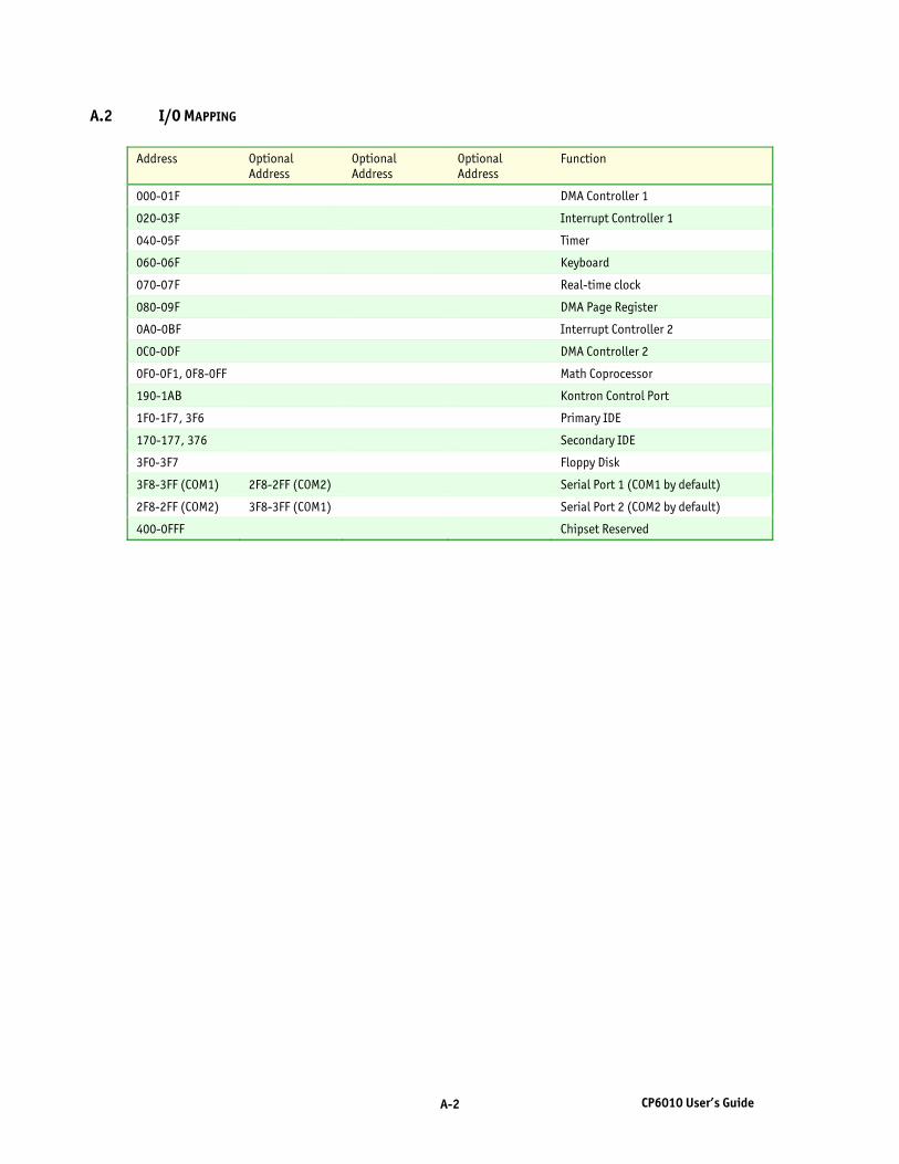
A-2 CP6010 User’s Guide
A.2 I/O MAPPING Address Optional
Address Optional Address
Optional Address
Function
000-01F DMA Controller 1
020-03F Interrupt Controller 1
040-05F Timer
060-06F Keyboard
070-07F Real-time clock
080-09F DMA Page Register
0A0-0BF Interrupt Controller 2
0C0-0DF DMA Controller 2
0F0-0F1, 0F8-0FF Math Coprocessor
190-1AB Kontron Control Port
1F0-1F7, 3F6 Primary IDE
170-177, 376 Secondary IDE
3F0-3F7 Floppy Disk
3F8-3FF (COM1) 2F8-2FF (COM2) Serial Port 1 (COM1 by default)
2F8-2FF (COM2) 3F8-3FF (COM1) Serial Port 2 (COM2 by default)
400-0FFF Chipset Reserved
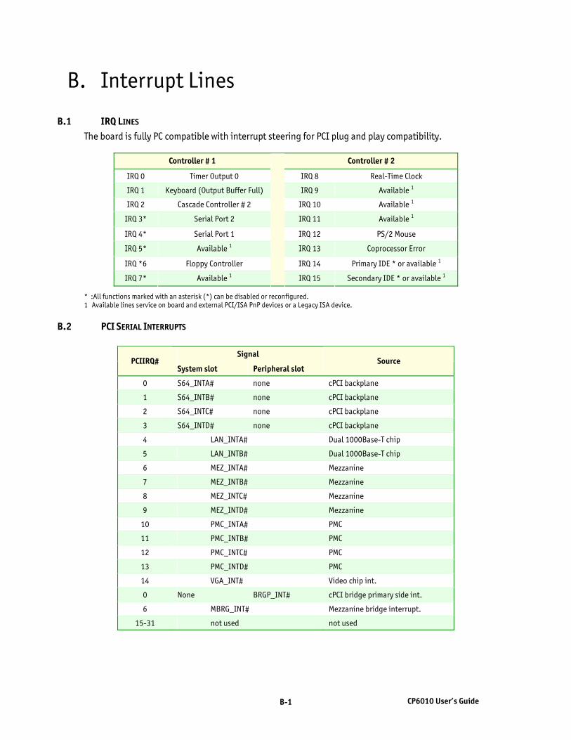
B-1 CP6010 User’s Guide
B. Interrupt Lines
B.1 IRQ LINES The board is fully PC compatible with interrupt steering for PCI plug and play compatibility.
Controller # 1 Controller # 2
IRQ 0 Timer Output 0 IRQ 8 Real-Time Clock
IRQ 1 Keyboard (Output Buffer Full) IRQ 9 Available 1
IRQ 2 Cascade Controller # 2 IRQ 10 Available 1
IRQ 3* Serial Port 2 IRQ 11 Available 1
IRQ 4* Serial Port 1 IRQ 12 PS/2 Mouse
IRQ 5* Available 1 IRQ 13 Coprocessor Error
IRQ *6 Floppy Controller IRQ 14 Primary IDE * or available 1
IRQ 7* Available 1
IRQ 15 Secondary IDE * or available 1
* :All functions marked with an asterisk (*) can be disabled or reconfigured. 1 Available lines service on board and external PCI/ISA PnP devices or a Legacy ISA device.
B.2 PCI SERIAL INTERRUPTS
Signal PCIIRQ#
System slot Peripheral slot Source
0 S64_INTA# none cPCI backplane
1 S64_INTB# none cPCI backplane
2 S64_INTC# none cPCI backplane
3 S64_INTD# none cPCI backplane
4 LAN_INTA# Dual 1000Base-T chip
5 LAN_INTB# Dual 1000Base-T chip
6 MEZ_INTA# Mezzanine
7 MEZ_INTB# Mezzanine
8 MEZ_INTC# Mezzanine
9 MEZ_INTD# Mezzanine
10 PMC_INTA# PMC
11 PMC_INTB# PMC
12 PMC_INTC# PMC
13 PMC_INTD# PMC
14 VGA_INT# Video chip int.
0 None BRGP_INT# cPCI bridge primary side int.
6 MBRG_INT# Mezzanine bridge interrupt.
15-31 not used not used

C-1 CP6010 User’s Guide
C. Kontron Extension Registers
C.1 FPGA/CPLD REGISTERS DEFINITION Unused (shaded) bits are reserved. It is strongly recommended not to modify unused bit to insure compatibility with other product. The base address is fixed. Bits marked NU are not used on this board. Writing to such bit does nothing and reading is undefined; either 0 or 1 may be returned. Bits with name in green and italics are for reference only; they are used on other Kontron CPCI SBC but not on this board.
Legend:
Symbol Signification U = Unchanged (stay unchanged after reset) X = Not Defined (bit not used on this board) NU = Not Used

C-2 CP6010 User’s Guide
C.2 OVERVIEW FPGA/CPLD registers
Address D7 D6 D5 D4 D3 D2 D1 D0
READ 0x190 NU NU NU RS485 RS232 ST1 NU NU
WRITE 0x190 NU NU NU RS485 RS232 ST1 NU NU
READ 0x191 PBRST WDO1 WDO ENPOST HD_ACT RED GREEN PFO
WRITE 0x191 NU NU NU ENPOST HD_ACT RED GREEN NU
READ 0x192 BL_ST BL_EN SW_O NU NU LOCK NU CLRHIS
WRITE 0x192 BL_ST BL_EN NU NU NU LOCK NU CLRHIS
READ 0x193 NU NU NU NU IDCHIP NU I2C_CLK I2C_DATA
WRITE 0x193 NU NU NU NU IDCHIP NU I2C_CLK I2C_DATA
READ 0x194 CND3 CIS3_1 CIS3_0 CBAS3_1 CBAS3_0 NU NU NU
WRITE 0x194 CND3 CIS3_1 CIS3_0 CBAS3_1 CBAS3_0 NU NU NU
READ 0x195 CND4 CIS4_1 CIS4_0 CBAS4_1 CBAS4_0 NU NU NU
WRITE 0x195 CND4 CIS4_1 CIS4_0 CBAS4_1 CBAS4_0 NU NU NU
READ 0x196 WDEN WDD2 WDD1 WDD0 NU NU NU NU
WRITE 0x196 WDEN WDD2 WDD1 WDD0 NU NU NU NU
READ 0x197 BATFEN BATFLT FANFEN FANFLT SWNIMEN SWNMI WDNMIEN WDNMI
WRITE 0x197 BATFEN NU FENFEN NU SWNMIEN NU WDNMIEN NU
READ 0x198 NU NU NU NU NU NU NU NU
WRITE 0x198 NU NU NU NU NU NU NU NU
READ 0x199 NU NU NU NU NU NU NU NU
WRITE 0x199 NU NU NU NU NU NU NU NU
READ 0x19A NU NU NU NU NU NU NU NU
WRITE 0x19A NU NU NU NU NU NU NU NU
READ 0x19B ST2 ST1 ST0 GA4 GA3 GA2 GA1 GA0
WRITE 0x19B NU NU NU NU NU NU NU NU
READ 0x19C TEST NU NU POST_COM BMC_TAKE_COM BMC_COM BMC_RST BMC_PRG
WRITE 0x19C NU NU NU POST_COM NU BMC_COM BMC_RST BMC_PRG
READ 0x19D NU HEALTHY SPEED2 SPEED1 SPEED0 JMP2 JMP1 JMP0
WRITE 0x19D NU NU RSV RSV RSV RSV RSV RSV
READ 0x19E NU NU NU NU NU NU NU NU
WRITE 0x19E NU NU NU NU NU NU NU NU
READ 0x19F NU NU NU NU NU NU NU NU
WRITE 0x19F NU NU NU NU NU NU NU NU
READ 0x1A0 0 0 0 0 Interrupt number
WRITE 0x1A0 NU NU NU NU Interrupt number
READ 0x1A1 NU NU I2C_EN NU NU SW_EN WD_EN ENUM_EN
WRITE 0x1A1 NU NU I2C_EN NU NU SW_EN WD_EN ENUM_EN
READ 0x1A2 NU NU I2C NU NU SWITCH WDOG ENUM
WRITE 0x1A2 NU NU I2C NU NU SWITCH WDOG NU
READ 0x1A3 NU NU JEN TRST TMS TCK TDO TDI
WRITE 0x1A3 NU NU JEN TRST TMS TCK NU TDI
READ 0x1A8 NU NU
WRITE 0x1A8 I2C address R/W#

C-3 CP6010 User’s Guide
FPGA/CPLD registers (continued) Address D7 D6 D5 D4 D3 D2 D1 D0
READ 0x1A9 Write Data
WRITE 0x1A9 NU
READ 0x1AA Read data
WRITE 0x1AA Write trigger read cycle
READ 0x1AB V1 V0 BUSY OPEN TXACK RXACK SCL pin SDA pin
WRITE 0x1AB NU NU NU OPEN TXACK NU SCL SDA
C.3 0190H: COM2 RS232/422/485 BUFFER CONTROL (FPGA)
Address Action D7 D6 D5 D4 D3 D2 D1 D0
READ NU NU NU RS485 RS232 ST1 NU NU
WRITE NU NU NU RS485 RS232 ST1 NU NU 0x190
Reset X X X 0 1 0 X X
RS485 RS232 ST1 Description
0 1 X RS232 mode (default)
1 0 0 RS485/422 point-to-point mode: - RX is always enable. - TX enabled when COM2 RTS is asserted.
1 0 1 RS485 party line mode: - RX enabled when COM2 RTS is deasserted. - TX enabled when COM2 RTS is asserted.
1 1 X Illegal. This puts the buffers in RS232 mode.
0 0 X Illegal. This puts the buffers in RS232 mode.
C.4 0191H: RESET HISTORY (FPGA)
About debug LED: The idea is that the LED will light red when in reset. (This is hardware.) As soon as the FPGA is programmed, the LED lights yellow if in reset, and the FPGA is enabled for post-code display (see below). If the BIOS fails, it is possible to read the last post code. If the BIOS succeeds, it will disable the post code and enable HD activity on the green LED. When neither post code or the hard disk LED is enabled, software can control LED state with Bit 1 and 2. If both the post code and hard drive activity are enabled, the LED control is given to BMC (on rev 1 only).
How to read the 8 bit post-code:
• Yellow: start of post sequence. • Red blink: This is the high nibble. 0 to 15 blinks represent hexadecimal 0 to F. • Green blink: This is the low nibble. 0 to 15 blinks represent hexadecimal 0 to F.
Address Action D7 D6 D5 D4 D3 D2 D1 D0
READ PBRST WDO1 WDO ENPOST HD_ACT RED GREEN PFO
WRITE NU NU NU ENPOST HD_ACT RED GREEN NU
Reset U X U 1 0 1 1 X 0x191
Power-up 0 X 0 1 0 1 1 X

C-4 CP6010 User’s Guide
PBRST Pushbutton reset. WDO Watchdog reset ENPOST Enable usage of the debug LED to display the last post code of the boot. HD_ACT Setting this bit will tie IDE_ACT to the red LED RED Set this bit to turn on the red LED. GREEN Set this bit to turn on the green LED.
History can be cleared by toggling the CLRHIS# bit in register 192h.
C.5 0192H: BRACKET SWITCH, BLUE LED, LOCK AND HISTORY (FPGA & CPLD)
Address Action D7 D6 D5 D4 D3 D2 D1 D0
READ BL_ST BL_EN SW_O NU NU LOCK NU CLRHIS#WRITE BL_ST BL_EN NU NU NU LOCK NU CLRHIS#0x192 Reset 0 0 U X X 1 X 1
BL_ST Blue LED state. BL_EN Blue LED control enable. Bios should enable this bit if the onboard bridge is disabled or in system
slot. SW_O When “1”, the bracket switch is open. LOCK When “1”, the enable bit of the watchdog (WDEN) can’t be modified. CLRHIS# Clear and bring back to 1 to clear the reset history.
C.6 0193H: ID CHIP AND I2C LINK (FPGA)
ID chip is a single wire interface. This chip can also be read by the onboard BMC microcontroller. It is recommended that if you use the IPMI function on the T6010, use the standard IPMI interface to retrieve board ID. I2C is a bit-banging interface. Use of register 1A8h to 1ABh is recommended as the new interface to onboard I2C memory.
Address Action D7 D6 D5 D4 D3 D2 D1 D0
READ NU NU NU NU IDCHIP NU SCL pin SDA pin
WRITE NU NU B NU
NU IDCHIP NU SCL SDA 0x193
Reset X X X X 1 X 1 1
IDCHIP ID Chip (serial number) control. Open-drain output with pin readback. I2C_SCL I2C clock. Totem pole output. I2C_SDA I2C data. Open-drain output with pin readback.

C-5 CP6010 User’s Guide
C.7 0196H: WATCHDOG CONTROL (FPGA) This is a “Kontron SBC” standard dual stage watchdog. However, the second stage time increases from 1ms to 16ms to ease the interrupt handling when using ISA interrupt. So, either a NMI or a legacy interrupt will generate after the specified timeout. Then, the watchdog must be triggered either by writing the WDD[2:0] bits or by clearing the interrupt bit in the 1A2h register. Failure to trigger the watchdog within 16ms will reset the system. If interrupts are disabled, the watchdog reverts to a single stage one.
Address Action D7 D6 D5 D4 D3 D2 D1 D0
READ WDEN WDD2 WDD1 WDD0 NU NU NU NU
WRITE WDEN WDD2 WDD1 WDD0 NU NU NU NU 0x196
Reset 0 1 1 1 X X X X
WDEN Enable. Lockable with bit LOCK. WDD[2..0] Timeout selection. A write to this register triggers the watchdog. Timeout as follow:
000: 0.016s 001: 0.065s 010: 0.262s 011: 1.048s 100: 4.194s 101: 16.78s 110: 67.11s 111: 268.4s
C.8 0197H: NMI ENABLES AND SOURCES (FPGA)
Address Action D7 D6 D5 D4 D3 D2 D1 D0
READ BATFEN BATFLT FANFEN FANFLT SWNMIEN SWNMI WDNMIEN WDNMI
WRITE BATFEN NU FANFEN NU SWNMIEN NU WDNMIEN NU 0x197
Reset X X X X 0 0 0 0
WDNMIEN Enable NMI generation for watchdog. WDNMI Watchdog NMI request. Will clear itself on a watchdog trigger. SWNMIEN Enable NMI generation for CPCI handle switch SWNMI Handle switch NMI request. Cleared by disabling SWNMIEN.
C.9 019BH: BACKPLANE INFORMATION (CPLD)
Address Action D7 D6 D5 D4 D3 D2 D1 D0
READ ST2 ST1 ST0 GA4 GA3 GA2 GA1 GA0
WRITE NU NU NU NU NU NU NU NU 019Bh
Reset State of hardware pins
GA[4..0] Geographical address. ST[2..0] Segment type (As defined in PICMG2.0R3.0 ECR#2).
000: Nominal left 001: Nominal right 111: Backplane do not provide segment type other: reserved

C-6 CP6010 User’s Guide
C.10 019CH: BMC CONTROL (CPLD)
Address Action D7 D6 D5 D4 D3 D2 D1 D0
READ TEST NU NU POST BMC_TAKE_COM BMC_COM BMC_RST BMC_PRG
WRITE NU NU NU POST NU BMC_COM BMC_RST BMC_PRG0x19C
Reset U X X 0 U 0 0 0
TEST If set, the SBC is inserted in a CPCI test backplane. This is used for Kontron test platform. POST_COM When ‘1’, COM2 is used to output post code BMC_TAKE_COM When ‘1’, BMC request COM2 usage. BMC_COM When '1', the SIO is connected to BMC.
When ‘0’, the SIO is connected to output buffer. This bit is ignored if BMC_TAKE_COM = ‘1’.
BMC_RST When '1', BMC is in reset. Write 1 to this register to put BMC in reset. Reading this bit read the actual signal state which can be held in reset by a jumper.
BMC_PRG When '1', set BMC in program mode. COM2 is redirected to BMC to allow bootstrapping the microcontroller.
Signal routing follow this table:
POST_COM BMC_PRG BMC_TAKE_COM2 BMC_COM Routing 0 0 0 0 SIO to buffers 0 0 0 1 SIO to BMC 0 0 1 X BMC to buffer 0 1 X X SIO to BMC 1 0 X 0 Post code to buffer (115200 baud)
C.11 019DH: PCI STATUS REGISTER (CPLD)
Address Action D7 D6 D5 D4 D3 D2 D1 D0
READ NU HEALTH SPEED2 SPEED1 SPEED0 JMP2 JMP1 JMP0
WRITE NU NU NU NU NU JMP2 JMP1 JMP0
Reset X U U U U U U U 0x19D
Power-up X NU NU NU NU Latch from jumper
JMP[2..0] Jumper settings to define the maximum allowable speed. SPEED[2..0] Detected bus speed according to PCIXCAP and M66EN PCI signals. HEALTH Healthy condition on bridge. If 0, the bridge is disabled.
Value Description for JMP[2:0] Description for SPEED[2:0] 000 Maximum speed is PCI 33MHz Current speed is PCI 33MHz 001 Maximum speed is PCI 66MHz Current speed is PCI 66MHz 010 Reserved Reserved 011 Reserved Reserved 100 Disable bridge in I/O slot Reserved 101 Reserved Reserved 110 Disable bridge Reserved 111 Reserved Reserved

C-7 CP6010 User’s Guide
C.12 01A0H: INTERRUPT NUMBER (FPGA)
Address Action D7 D6 D5 D4 D3 D2 D1 D0
READ NU NU NU NU INT
WRITE NU NU NU NU INT 0x1A0
Reset X X X X 0h
This register holds the interrupt number on which the FPGA/CPLD is mapped. It is written by the BIOS on boot and read by the software application. This is a legacy ISA interrupt so the range is from 0 to 15. Valid values in this register are 5 and 7.
7:4 Undefined 3:0 Interrupt number 0h to Fh. Other than 5h and 7h are invalid and disable interrupt.
C.13 01A1H: INTERRUPT ENABLE (FPGA)
Address Action D7 D6 D5 D4 D3 D2 D1 D0
READ NU NU I2C_EN NU NU SW_EN WD_EN ENUM_EN
WRITE NU NU I2C_EN NU NU SW_EN WD_EN ENUM_EN0x1A1
Reset X X 0 X X 0 0 0
I2C_EN Enable I2C interrupt on falling edge of BUSY bit (1ABh) SW_EN Enable interrupt on switch event. WD_EN Enable watchdog interrupt ENUM_EN Enable ENUM interrupt. The interrupt is generated for both onboard CPCI interface and the
mezzanine CPCI interface. *** If more than one software driver access this register, take care to race condition.
Atomic modify/write may be needed.
C.14 01A2H: PCI INTERRUPT STATUS (FPGA)
Address Action D7 D6 D5 D4 D3 D2 D1 D0
READ NU NU I2C NU NU SWITCH WDOG ENUM
WRITE NU NU I2C NU NU SWITCH WDOG NU 0x1A2
Reset X X 0 X X 0 0 0
I2C A one indicates the BUSY bit has transition from 1 to 0, thus the I2C engine is ready for new data.
Write a one to clear this interrupt. SWITCH A one indicates a switch event has occurred. Switch state can be read on 0191h bit 5. Write a one
to this bit clear the interrupt. WDOG A one indicates a watchdog interrupt has occurred. Writing a one to this bit clears the watchdog
and clears the interrupt. Reset will occur 16ms after the interrupt. ENUM A one indicates an ENUM has occurred on either the onboard CPCI interface or the mezzanine
interface. Writing a one to this register does nothing. The interrupt condition must be cleared in the source PCI device.
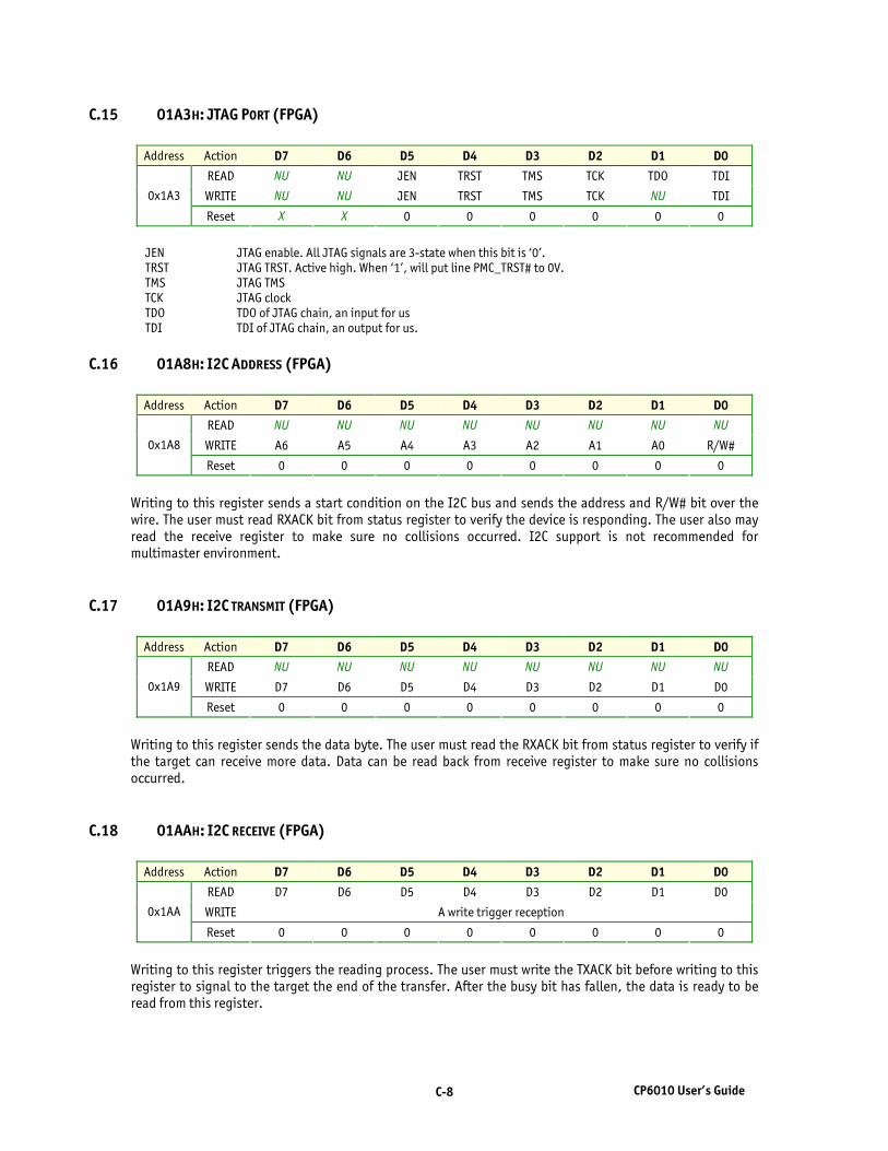
C-8 CP6010 User’s Guide
C.15 01A3H: JTAG PORT (FPGA)
Address Action D7 D6 D5 D4 D3 D2 D1 D0
READ NU NU JEN TRST TMS TCK TDO TDI
WRITE NU NU JEN TRST TMS TCK NU TDI 0x1A3
Reset X X 0 0 0 0 0 0
JEN JTAG enable. All JTAG signals are 3-state when this bit is ‘0’. TRST JTAG TRST. Active high. When ‘1’, will put line PMC_TRST# to 0V. TMS JTAG TMS TCK JTAG clock TDO TDO of JTAG chain, an input for us TDI TDI of JTAG chain, an output for us.
C.16 01A8H: I2C ADDRESS (FPGA)
Address Action D7 D6 D5 D4 D3 D2 D1 D0
READ NU NU NU NU NU NU NU NU
WRITE A6 A5 A4 A3 A2 A1 A0 R/W# 0x1A8
Reset 0 0 0 0 0 0 0 0
Writing to this register sends a start condition on the I2C bus and sends the address and R/W# bit over the wire. The user must read RXACK bit from status register to verify the device is responding. The user also may read the receive register to make sure no collisions occurred. I2C support is not recommended for multimaster environment.
C.17 01A9H: I2C TRANSMIT (FPGA)
Address Action D7 D6 D5 D4 D3 D2 D1 D0 READ NU NU NU NU NU NU NU NU
WRITE D7 D6 D5 D4 D3 D2 D1 D0 0x1A9
Reset 0 0 0 0 0 0 0 0
Writing to this register sends the data byte. The user must read the RXACK bit from status register to verify if the target can receive more data. Data can be read back from receive register to make sure no collisions occurred.
C.18 01AAH: I2C RECEIVE (FPGA)
Address Action D7 D6 D5 D4 D3 D2 D1 D0
READ D7 D6 D5 D4 D3 D2 D1 D0
WRITE A write trigger reception 0x1AA
Reset 0 0 0 0 0 0 0 0
Writing to this register triggers the reading process. The user must write the TXACK bit before writing to this register to signal to the target the end of the transfer. After the busy bit has fallen, the data is ready to be read from this register.

C-9 CP6010 User’s Guide
C.19 01ABH: I2C FLAGS (FPGA)
Address Action D7 D6 D5 D4 D3 D2 D1 D0
READ V1 V0 BUSY OPEN TXACK RXACK SCL pin SDA pin
WRITE NU NU NU OPEN TXACK NU SCL SDA 0x1AB
Reset NU NU NU 0 0 NU 1 1
V1, V0 Version of the I2C engine. Currently 0, 0. This may be used for future enhancement and to ease
software usability from one Kontron product to the other. BUSY When one, the I2C engine is busy. OPEN When one, a transaction is proceeding. User must clear this bit to send a STOP condition at the end
of a transaction. TXACK When one, send a NACK when reading the next byte. If zero, send an ACK. RXACK When one, last write ended with a NACK; when zero, it ends with an ACK. SCL Reading reflects the state of the pin. Writing may be used to implement bit-banging interface. SDA Reading reflects the state of the pin. Writing may be used to implement bit-banging interface.

D-1 CP6010 User’s Guide
D. Connector Pinouts D.1 CONNECTORS AND HEADERS SUMMARY
Connector Description
J1 CPCI Bus connector
J2 CPCI Bus connector
J3 CPCI I/O connector
J4 CPCI I/O connector
J5 CPCI I/O connector
J6 COM1 – RS-232 (Faceplate, front panel configuration only)
J7 USB2 (Faceplate, front panel configuration only)
J8 CRT VGA Connector (Faceplate, front panel configuration only)
J9, J10 Ethernet LAN2 and LAN1 connectors (Front panel configuration only)
J13, J14 CPU Sockets
J15-J18 DIMM Sockets
J20 Hot Swap switch
J21 POST Code
J22 Power Connector
J23 IDE Mezzanine card
JN1 –JN4 64Bit PCIX Mezzanine
SW1 Reset Switch
BT1 CMOS Battery Backup connector

D-2 CP6010 User’s Guide
D.2 CPCI BUS (J1)
Pin ROW A ROW B ROW C ROW D ROW E
1 VCC5E -12VE RSV +12VE VCCE
2 RSV VCCE RSV RSV RSV
3 INTA# INTB# INTC# VCCE INTD#
4 IPMB_PWR HEALTHY# VI/O INTP INTS
5 RSV RSV RST# GND GNT0#
6 REQ0# PCI_PRESENT# VCC3E CLK0 AD31
7 AD30 AD29 AD28 GND AD27
8 AD26 GND VI/O AD25 AD24
9 CBE3# IDSEL AD23 GND AD22
10 AD21 GND VCC3E AD20 AD19
11 AD18 AD17 AD16 GND CBE2#
12
13
14
KEY AREA
15 VCC3E FRAME# IRDY# BD_SEL# TRDY#
16 DEVSEL# PCIXCAP VI/O STOP# LOCK#
17 VCC3E IPMB0_SCL IPMB0_SDA GND PERR#
18 SERR# GND VCC3E PAR CBE1#
19 VCC3E AD15 AD14 GND AD13
20 AD12 GND VI/O AD11 AD10
21 VCC3E AD9 AD8 M66EN CBE0#
22 AD7 GND VCC3E AD6 AD5
23 VCC3E AD4 AD3 VCCE AD2
24 AD1 VCCE VI/O AD0 ACK64#
25 VCCE REQ64# ENUM# VCC3E VCCE
# Active Low
Long pins : 3D, 4C,5D, 6C, 7D, 9D, 10D, 17D, 19D, 22C, 23D, 24C
Short pins : 9B, 15D

D-3 CP6010 User’s Guide
D.3 CPCI BUS (J2)
Pin ROW A ROW B ROW C ROW D ROW E
1 S_CLK1 GND REQ1# GNT1# REQ2#
2 S_CLK2 S_CLK3 SYSEN# GNT2# REQ3#
3 S_CLK4 GND GNT3# REQ4# GNT4#
4 V I/O RSV CBE7# GND CBE6#
5 CBE5# 64_EN# V I/O CBE4# PAR64
6 AD63 AD62 AD61 GND AD60
7 AD59 GND V I/O AD58 AD57
8 AD56 AD55 AD54 GND AD53
9 AD52 GND V I/O AD51 AD50
10 AD49 AD48 AD47 GND AD46
11 AD45 GND V I/O AD44 AD43
12 AD42 AD41 AD40 GND AD39
13 AD38 GND V I/O AD37 AD36
14 AD35 AD34 AD33 GND AD32
15 RSV GND *FAL# REQ5# GNT5#
16 RSV RSV *DEG# GND RSV
17 RSV GND PRST# REQ6# GNT6#
18 RSV RSV RSV GND RSV
19 GND GND IMPB1_SDA SMB1_SCL SMB_ALERT#
20 CLK5 GND RSV GND RSV
21 CLK6 GND RSV RSV RSV
22 GA4 GA3 GA2 GA1 GA0
* Not Used, # Active Low

D-4 CP6010 User’s Guide
D.4 CPCI BUS (J3)
Pin ROW A ROW B ROW C ROW D ROW E
1 COM1:RTS COM1:RXD COM1:DSR COM1:DCD ID1
2 COM1:RI COM1:DTR COM1:CTS COM1:TXD MOUSE:CLK
3 COM2:RTS COM2:RXD COM2:DSR COM2:DCD MOUSE:DATA
4 COM2:RI COM2:DTR COM2:CTS COM2:TXD KB:DATA
5 VGA:BLUE VGA:HSYNC VGA:VSYNC VGA:SCL KB:CLK
6 VGA:RED VGA:GREEN VGA:SDA POST:CLK POST:DATA
7 ID0 ID2 ID3 ID4 SPEAKER
8 USB0:DATA- USB0:DATA+ RSV RSV RSV
9 USB1:DATA- USB1:DATA+ RSV RSV RSV
10 USB1:VCC USB0:VCC RSV RSV RSV
11 RSV RSV RSV RSV RSV
12 RSV RSV RSV RSV RSV
13 LAN0:ACT LAN1:ACT RSV RSV RSV
14 LAN0:LINK LAN1:LINK LAN:CT RSV RSV
15 LAN1:DB+ LAN1:DB- GND LAN1:DD+ LAN1:DD-
16 LAN1:DA+ LAN1:DA- GND LAN1:DC+ LAN1:DC-
17 LAN0:DB+ LAN0:DB- GND LAN0:DD+ LAN0:DD-
18 LAN0:DA+ LAN0:DA- GND LAN0:DC+ LAN0:DC-
19 VCC VCC VCC3 +12V -12V

D-5 CP6010 User’s Guide
D.5 CPCI BUS ( PIM ) (J4)
Pin ROW A ROW B ROW C ROW D ROW E
1 PIM:61 PIM:63 GND PIM:62 PIM:64
2 PIM:57 PIM:59 GND PIM:58 PIM:60
3 GND GND GND GND GND
4 PIM:53 PIM:55 GND PIM:54 PIM:56
5 PIM:49 PIM:51 GND PIM:50 PIM:52
6 GND GND GND GND GND
7 PIM:45 PIM:47 GND PIM:46 PIM:48
8 PIM:41 PIM:43 GND PIM:42 PIM:44
9 GND GND GND GND GND
10 PIM:37 PIM:39 GND PIM:38 PIM:40
11 PIM:33 PIM:35 GND PIM:34 PIM:36
12
13
14
KEY AREA
15 PIM:29 PIM:31 GND PIM:30 PIM:32
16 PIM:25 PIM:27 GND PIM:26 PIM:28
17 GND GND GND GND GND
18 PIM:21 PIM:23 GND PIM:22 PIM:24
19 PIM:17 PIM:19 GND PIM:18 PIM:20
20 GND GND GND GND GND
21 PIM:13 PIM:15 GND PIM:14 PIM:16
22 PIM:9 PIM:11 GND PIM:10 PIM:12
23 N.C. VCC GND N.C. VCC3
24 PIM:5 PIM:7 GND PIM:6 PIM:8
25 PIM:1 PIM:3 GND PIM:2 PIM:4

D-6 CP6010 User’s Guide
D.6 CPCI BUS ( SCSI) (J4)
Pin ROW A ROW B ROW C ROW D ROW E
1 D12+ D12- GND D13+ D13-
2 D14+ D14- GND D15+ D15-
3 GND GND GND GND GND
4 DPH+ DPH- GND D0+ D0-
5 D1+ D1- GND D2+ D2-
6 GND GND GND GND GND
7 D3+ D3- GND D4+ D4-
8 D5+ D5- GND D6+ D6-
9 GND GND GND GND GND
10 D7+ D7- GND DPL+ DPL-
11 DIFFSENS TERMPWR7 GND TERMPWR8 TERMPWR9
12
13
14
KEY AREA
15 TERMPWR3 TERMPWR4 GND TERMPWR5 TERMPWR6
16 TERMPWR1 TERMPWR2 GND ATN+ ATN-
17 GND GND GND GND GND
18 BSY+ BSY- GND ACK+ ACK-
19 RST+ RST- GND MSG+ MSG-
20 GND GND GND GND GND
21 SEL+ SEL- GND CD+ CD-
22 REQ+ REQ- GND IO+ IO-
23 N.C. VCC GND N.C. VCC3
24 D8+ D8- GND D9+ D9-
25 D10+ D10- GND D11+ D11-

D-7 CP6010 User’s Guide
D.7 CPCI BUS (J5)
Pin ROW A ROW B ROW C ROW D ROW E
1 RSV RSV GND RSV RSV
2 RSV RSV GND RSV RSV
3 RSV RSV GND RSV RSV
4 RSV RSV GND RSV RSV
5 RSV RSV GND RSV RSV
6 RSV RSV GND RSV RSV
7 RSV RSV GND RSV RSV
8 RSV RSV GND RSV RSV
9 RSV RSV GND RSV RSV
10 FD:MSEN0 FD:MSEN1 GND RSV RSV
11 FD:MTR0# FD:INDEX# GND FD:FDEDIN# FD:DENSEL#
12 FD: DIR# FD: MTR1# GND FD: DSEL0# FDE: DSEL1#
13 FD: TRK0# FD: WGATE# GND FD: WDATA# FD: STEP#
14 FD: DSKCHG# FD: HDSEL# GND FD: RDATA# FD: WRPROT#
15 IDE1:D6 IDE1:D8 GND IDE1:D7 IDE1:RESET#
16 IDE1:D4 IDE1:D10 GND IDE1:D5 IDE1:D9
17 IDE1:D2 IDE1:D12 GND IDE1:D3 IDE1:D11
18 IDE1:D0 IDE1:D14 GND IDE1:D1 IDE1:D13
19 IDE1:IOR# IDE1:IOW# GND IDE1:DMARQ IDE1:D15
20 IDE1:IOCS16# IDE1:IRQ GND IDE1:DMACK# IDE1:IORDY
21 IDE1:A2 IDE1:A0 GND IDE1:A1 IDE1:PDIAG#
22 IDE1:ACT# IDE1:CS1# GND IDE1:CS0# RSV
# Active Low
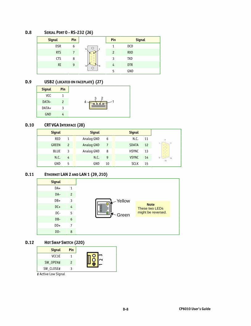
D-8 CP6010 User’s Guide
D.8 SERIAL PORT 0 - RS-232 (J6)
Signal Pin Pin Signal
DSR 6 1 DCD
RTS 7 2 RXD
CTS 8 3 TXD
RI 9 4 DTR
5 GND
D.9 USB2 (LOCATED ON FACEPLATE) (J7)
Signal Pin
VCC 1
DATA- 2
DATA+ 3
GND 4
D.10 CRT VGA INTERFACE (J8)
Signal Signal Signal
RED 1 Analog GND 6 N.C. 11
GREEN 2 Analog GND 7 SDATA 12
BLUE 3 Analog GND 8 HSYNC 13
N.C. 4 N.C. 9 VSYNC 14
GND 5
GND 10 SCLK 15
D.11 ETHERNET LAN 2 AND LAN 1 (J9, J10)
Signal
DA+ 1
DA- 2
DB+ 3
DC+ 4
DC- 5
DB- 6
DD+ 7
DD- 8
D.12 HOT SWAP SWITCH (J20)
Signal Pin
VCC3E 1
SW_OPEN# 2
SW_CLOSE# 3
# Active Low Signal
1
8Yellow
Green
Note These two LEDs might be reversed.
12
3
11
1
6
111
10155
1 6
9 5
1
5
6
9
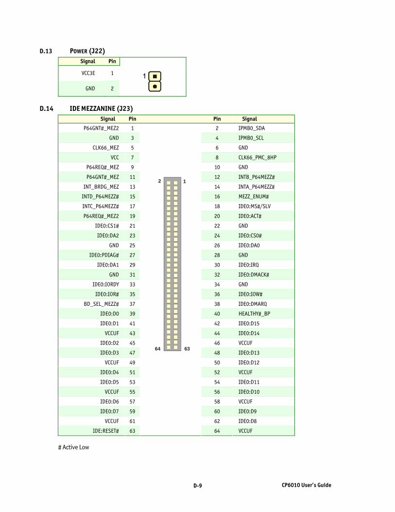
D-9 CP6010 User’s Guide
D.13 POWER (J22) Signal Pin
VCC3E 1
GND 2
D.14 IDE MEZZANINE (J23)
Signal Pin Pin Signal
P64GNT#_MEZ2 1 2 IPMB0_SDA
GND 3 4 IPMB0_SCL
CLK66_MEZ 5 6 GND
VCC 7 8 CLK66_PMC_8HP
P64REQ#_MEZ 9 10 GND
P64GNT#_MEZ 11 12 INTB_P64MEZZ#
INT_BRDG_MEZ 13 14 INTA_P64MEZZ#
INTD_P64MEZZ# 15 16 MEZZ_ENUM#
INTC_P64MEZZ# 17 18 IDE0:MS#/SLV
P64REQ#_MEZ2 19 20 IDE0:ACT#
IDE0:CS1# 21 22 GND
IDE0:DA2 23 24 IDE0:CS0#
GND 25 26 IDE0:DA0
IDE0:PDIAG# 27 28 GND
IDE0:DA1 29 30 IDE0:IRQ
GND 31 32 IDE0:DMACK#
IDE0:IORDY 33 34 GND
IDE0:IOR# 35 36 IDE0:IOW#
BD_SEL_MEZZ# 37 38 IDE0:DMARQ
IDE0:D0 39 40 HEALTHY#_BP
IDE0:D1 41 42 IDE0:D15
VCCUF 43 44 IDE0:D14
IDE0:D2 45 46 VCCUF
IDE0:D3 47 48 IDE0:D13
VCCUF 49 50 IDE0:D12
IDE0:D4 51 52 VCCUF
IDE0:D5 53 54 IDE0:D11
VCCUF 55 56 IDE0:D10
IDE0:D6 57 58 VCCUF
IDE0:D7 59 60 IDE0:D9
VCCUF 61 62 IDE0:D8
IDE:RESET# 63
64 VCCUF
# Active Low
6364
12
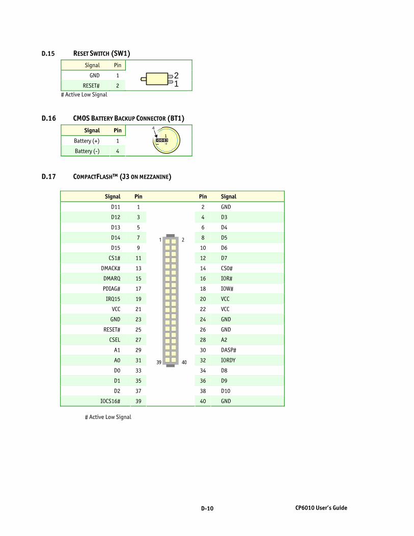
D-10 CP6010 User’s Guide
D.15 RESET SWITCH (SW1)
Signal Pin
GND 1
RESET# 2
# Active Low Signal
D.16 CMOS BATTERY BACKUP CONNECTOR (BT1)
Signal Pin
Battery (+) 1
Battery (-) 4
D.17 COMPACTFLASH™ (J3 ON MEZZANINE)
Signal Pin Pin Signal
D11 1 2 GND
D12 3 4 D3
D13 5 6 D4
D14 7 8 D5
D15 9 10 D6
CS1# 11 12 D7
DMACK# 13 14 CS0#
DMARQ 15 16 IOR#
PDIAG# 17 18 IOW#
IRQ15 19 20 VCC
VCC 21 22 VCC
GND 23 24 GND
RESET# 25 26 GND
CSEL 27 28 A2
A1 29 30 DASP#
A0 31 32 IORDY
D0 33 34 D8
D1 35 36 D9
D2 37 38 D10
IOCS16# 39
40 GND
# Active Low Signal
12
1
39
2
40
1
4
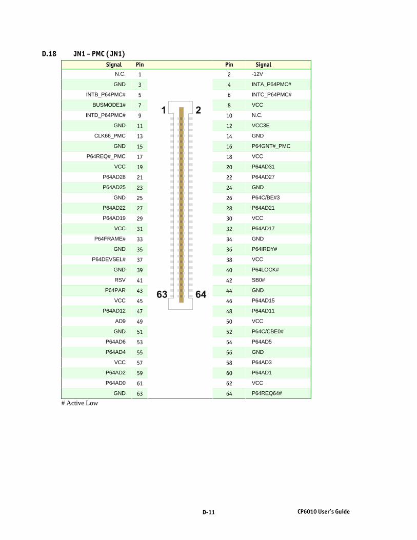
D-11 CP6010 User’s Guide
D.18 JN1 – PMC ( JN1) Signal Pin Pin Signal
N.C. 1 2 -12V
GND 3 4 INTA_P64PMC#
INTB_P64PMC# 5 6 INTC_P64PMC#
BUSMODE1# 7 8 VCC
INTD_P64PMC# 9 10 N.C.
GND 11 12 VCC3E
CLK66_PMC 13 14 GND
GND 15 16 P64GNT#_PMC
P64REQ#_PMC 17 18 VCC
VCC 19 20 P64AD31
P64AD28 21 22 P64AD27
P64AD25 23 24 GND
GND 25 26 P64C/BE#3
P64AD22 27 28 P64AD21
P64AD19 29 30 VCC
VCC 31 32 P64AD17
P64FRAME# 33 34 GND
GND 35 36 P64IRDY#
P64DEVSEL# 37 38 VCC
GND 39 40 P64LOCK#
RSV 41 42 SB0#
P64PAR 43 44 GND
VCC 45 46 P64AD15
P64AD12 47 48 P64AD11
AD9 49 50 VCC
GND 51 52 P64C/CBE0#
P64AD6 53 54 P64AD5
P64AD4 55 56 GND
VCC 57 58 P64AD3
P64AD2 59 60 P64AD1
P64AD0 61 62 VCC
GND 63
64 P64REQ64#
# Active Low
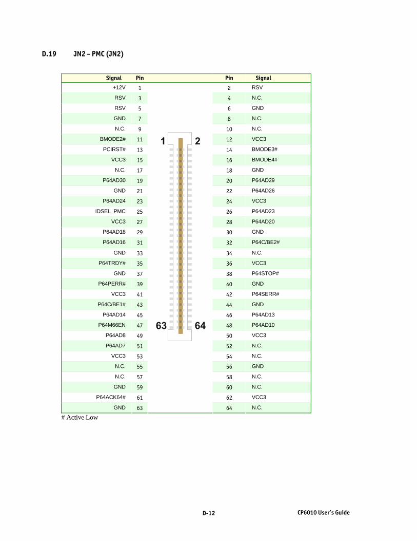
D-12 CP6010 User’s Guide
D.19 JN2 – PMC (JN2)
Signal Pin Pin Signal +12V 1 2 RSV
RSV 3 4 N.C.
RSV 5 6 GND
GND 7 8 N.C.
N.C. 9 10 N.C.
BMODE2# 11 12 VCC3
PCIRST# 13 14 BMODE3#
VCC3 15 16 BMODE4#
N.C. 17 18 GND
P64AD30 19 20 P64AD29
GND 21 22 P64AD26
P64AD24 23 24 VCC3
IDSEL_PMC 25 26 P64AD23
VCC3 27 28 P64AD20
P64AD18 29 30 GND
P64AD16 31 32 P64C/BE2#
GND 33 34 N.C.
P64TRDY# 35 36 VCC3
GND 37 38 P64STOP#
P64PERR# 39 40 GND
VCC3 41 42 P64SERR#
P64C/BE1# 43 44 GND
P64AD14 45 46 P64AD13
P64M66EN 47 48 P64AD10
P64AD8 49 50 VCC3
P64AD7 51 52 N.C.
VCC3 53 54 N.C.
N.C. 55 56 GND
N.C. 57 58 N.C.
GND 59 60 N.C.
P64ACK64# 61 62 VCC3
GND 63
64 N.C.
# Active Low
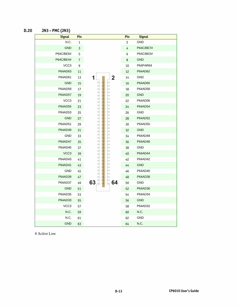
D-13 CP6010 User’s Guide
D.20 JN3 – PMC (JN3) Signal Pin Pin Signal
N.C. 1 2 GND
GND 3 4 P64C/BE7#
P64C/BE6# 5 6 P64C/BE5#
P64C/BE4# 7 8 GND
VCC3 9 10 P64PAR64
P64AD63 11 12 P64AD62
P64AD61 13 14 GND
GND 15 16 P64AD60
P64AD59 17 18 P64AD58
P64AD57 19 20 GND
VCC3 21 22 P64AD56
P64AD55 23 24 P64AD54
P64AD53 25 26 GND
GND 27 28 P64AD52
P64AD51 29 30 P64AD50
P64AD49 31 32 GND
GND 33 34 P64AD48
P64AD47 35 36 P64AD46
P64AD45 37 38 GND
VCC3 39 40 P64AD44
P64AD43 41 42 P64AD42
P64AD41 43 44 GND
GND 45 46 P64AD40
P64AD39 47 48 P64AD38
P64AD37 49 50 GND
GND 51 52 P64AD36
P64AD35 53 54 P64AD34
P64AD33 55 56 GND
VCC3 57 58 P64AD32
N.C. 59 60 N.C.
N.C. 61 62 GND
GND 63
64 N.C.
# Active Low
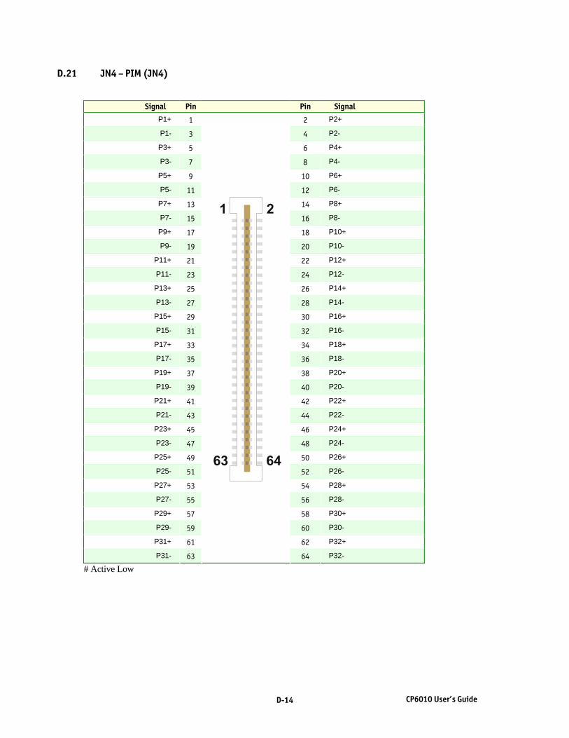
D-14 CP6010 User’s Guide
D.21 JN4 – PIM (JN4)
Signal Pin Pin Signal P1+ 1 2 P2+
P1- 3 4 P2-
P3+ 5 6 P4+
P3- 7 8 P4-
P5+ 9 10 P6+
P5- 11 12 P6-
P7+ 13 14 P8+
P7- 15 16 P8-
P9+ 17 18 P10+
P9- 19 20 P10-
P11+ 21 22 P12+
P11- 23 24 P12-
P13+ 25 26 P14+
P13- 27 28 P14-
P15+ 29 30 P16+
P15- 31 32 P16-
P17+ 33 34 P18+
P17- 35 36 P18-
P19+ 37 38 P20+
P19- 39 40 P20-
P21+ 41 42 P22+
P21- 43 44 P22-
P23+ 45 46 P24+
P23- 47 48 P24-
P25+ 49 50 P26+
P25- 51 52 P26-
P27+ 53 54 P28+
P27- 55 56 P28-
P29+ 57 58 P30+
P29- 59 60 P30-
P31+ 61 62 P32+
P31- 63
64 P32-
# Active Low

E-1 CP6010 User’s Guide
E. BIOS Setup Error Codes E.1 POST BEEP
Recoverable POST Errors Whenever a recoverable error occurs during POST, Phoenix BIOS displays an error message describing the problem.
Phoenix BIOS also issues a beep code (one long tone followed by two short tones) during POST if the video configuration fails (no card installed or faulty) or if an external ROM module does not properly checksum to zero.
An external ROM module (e. g. VGA) can also issue audible errors, usually consisting of one long tone followed by a series of short tones.
E.1.1 Terminal POST Errors
There are several POST routines that issue a POST Terminal Error and shut down the system if they fail. Before shutting down the system, the terminal error handler issues a beep code signifying the test point error, writes the error to port 80h, attempts to initialize the video, and writes the error in the upper left corner of the screen (using both mono and color adapters).
The routine derives the beep code from the test point error as follows:
1. The 8- bit error code is broken down to four 2 bit groups (Discard the most significant group if it
is 00). 2. Each group is made one- based (1 through 4) by adding 1. 3. Short beeps are generated for the number in each group. Example: Test point 01Ah = 00 01 10 10 = 1- 2- 3- 3 beeps Test Points and Beep Codes At the beginning of each POST routine, the BIOS outputs the test point error code to I/O address 80h. Use this code during troubleshooting to establish at what point the system failed and what routine was being performed.
If the BIOS detects a terminal error condition, it halts POST after issuing a terminal error beep code (See above) and attempting to display the error code on upper left corner of the screen and on the port 80h LED display.
If the system hangs before the BIOS can process the error, the value displayed at the port 80h is the last test performed. In this case, the screen does not display the error code.
Code Beeps POST Routine Description
02h Verify Real Mode
03h Disable Non-Maskable Interrupt (NMI)
04h Get CPU type
06h Initialize system hardware
07h De-shadow BIOS code
08h Initialize chipset with initial POST values
09h Set IN-POST flag, Verify CMOS and RTC validity

E-2 CP6010 User’s Guide
Code Beeps POST Routine Description
0Ah Initialize CPU registers
0Bh Enable CPU cache
0Ch Initialize caches to initial POST values
0Eh Initialize I/O component
0Fh Initialize the local bus IDE
10h Initialize Power Management
11h Load alternate registers with initial POST values
12h Restore CPU control word during warm boot
13h Initialize PCI Bus Mastering devices
14h Initialize keyboard controller
16h 1- 2- 2- 3 BIOS ROM checksum
17h Initialize cache before memory autosize
18h 8254 timer initialization
1Ah 8237 DMA controller initialization
1Ch Reset Programmable Interrupt Controller
20h 1- 3- 1- 1 Test DRAM refresh
22h 1- 3- 1- 3 Test 8742 Keyboard Controller
24h Set ES segment register to 4 GB
26h Enable A20 line
28h Autosize DRAM
29h Initialize POST Memory Manager
2Ah Clear 512 KB base RAM
2Bh Enhanced COMS init
2Ch 1- 3- 4- 1 RAM failure on address line xxxx *
2Eh 1- 3- 4- 3 RAM failure on data bits xxxx * of low byte of memorybus
2Fh Enable cache before system BIOS shadow
30h 1- 4- 1- 1 RAM failure on data bits xxxx * of high byte of memory bus
32h Test CPU bus- clock frequency
33h Initialize Phoenix Dispatch Manager
34h CMOS test (on Suspend-to-Disk resume)
35h Register re-initialization
36h Warm start shut down
38h Shadow system BIOS ROM
39h Cache re-initialization
3Ah Autosize cache
3Ch Advanced configuration of chipset registers
3Dh Load alternate registers with CMOS values
42h Initialize interrupt vectors
45h POST device initialization
46h 2- 1- 2- 3 Check ROM copyright notice
48h Check video configuration against CMOS

E-3 CP6010 User’s Guide
Code Beeps POST Routine Description
49h Initialize PCI bus and devices (I/O 81h = PCI Bus tested)
4Ah Initialize all video adapters in system
4Bh QuietBoot (logo) start
4Ch Shadow video BIOS ROM
4Eh Display BIOS copyright notice
4Fh Multi-Boot (Boot menu support) Initialization
50h Display CPU type and speed
51h Initialize EISA board
52h Test keyboard
54h Set key click if enabled
55h USB initialization (legacy support)
56h Enable Keyboard
58h 2- 2- 3- 1 Test for unexpected interrupts
59h Initialize POST display service
5Ah Display prompt "Press DEL to enter SETUP"
5Bh Disable CPU cache
5Ch Test RAM between 512 and 640 KB
60h Test extended memory
62h Test extended memory address lines
64h Jump to UserPatch1
66h Configure advanced cache registers
67h Early Initialize of Multi Processor APIC
68h Enable external and CPU caches
69h Setup System Management Mode (SMM) area
6Ah Display external L2 cache size
6Bh Load custom defaults (optional)
6Ch Display shadow- area message
6Eh Clear Memory
70h Display error messages
72h Test for configuration error detected
74h Test RTC
76h Check for keyboard errors
7Ch Set up hardware interrupt vectors
7Dh Intelligent System Monitoring initialization
7Eh Initialize coprocessor if present
80h Disable onboard Super I/O ports and IRQs for Auto-detection.
81h Late POST device initialization
82h Detect and install external RS232 ports
83h Configure non-Motherboard Configurable Device IDE controllers
84h Detect and install external parallel ports
85h Initialize PC-compatible PnP ISA devices

E-4 CP6010 User’s Guide
Code Beeps POST Routine Description
86h Re- initializes onboard I/O ports.
87h Configure Motherboard Configurable Devices (optional)
88h Initialize BIOS Data Area
89h Enable Non-Maskable Interrupts (NMIs)
8Ah Initialize Extended BIOS Data Area
8Bh Test and initialize PS/2 mouse
8Ch Initialize floppy controller
8Fh Determine number of ATA drives (optional)
90h Initialize hard-disk controllers, auto-detect IDE drives
91h Initialize local-bus hard-disk controllers
92h Jump to UserPatch2
93h Build MPTABLE for multi-processor boards
95h Install CD ROM for boot
96h Clear huge ES segment register
97h Fixup Multi Processor table
98h 1- 2 Search for option ROMs. One long, two short beeps on checksum failure
99h Check for SMART Drive (optional)
9Ch Set up Power Management
9Dh Initialize security engine (optional)
9Eh Enable hardware interrupts
9Fh Determine number of ATA and SCSI drives (optional)
A0h Set time of day
A4h Initialize Typematic rate
A8h Erase DEL prompt
AAh Scan for DEL key stroke
ACh Enter SETUP
AEh Clear Boot flag
B0h Check for errors
B2h POST done – prepare to boot operating system
B4h 1 One short beep before boot
B5h Terminate QuietBoot (optional)
B6h Check password (optional)
B7h ACPI initialization
B9h Prepare Boot
BAh Initialize DMI parameters
BCh Clear parity checkers
BDh Display MultiBoot menu
BEh Clear screen (optional)
BFh Display Summary Screen
C0h Try to boot with INT 19
C1h Initialize POST Error Manager (PEM)

E-5 CP6010 User’s Guide
Code Beeps POST Routine Description
C2h Save the current boot type into CMOS
C2h Initialize error logging
C3h Check the requested boot type (Cold or Warm)
C3h Initialize error display function
C4h Initialize system error handler
C4h Install the IRQ1 vector for BIOS Hot Keys
C5h PnP NoteDock dual CMOS (optional)
C5h Mark the fact that we are no longer in POST
C6h Console Redirection SIO Initialize
C7h Remove Console Redirection
C8h Force Emergency Flash update check (Ctrl-E and bad CMOS)
C8h Test Gate A20
C9h Extended checksum (optional)
CDh Install Console Redirection Interrupt Handler
CFh Extended BIOS data Fail
D1h BIOS stack initialization
D2h Unknown interrupt
D3h Setup WAD (reserved memory used by BIOS)
D4h Get CPU string
E0h Software SMI failure during POST

E-6 CP6010 User’s Guide
Code Beeps For Boot Block in Flash ROM
80h Initialize the chipset
81h Initialize the bridge
82h Initialize the CPU
83h Initialize system timer
84h Initialize system I/O
85h Check force recovery boot
86h Checksum BIOS ROM
87h Go to BIOS
88h Set Huge Segment
89h Initialize Multi Processor
8Ah Initialize OEM special code
8Bh Initialize PIC and DMA
8Ch Initialize Memory type
8Dh Initialize Memory size
8Eh Shadow Boot Block
8Fh System memory test
90h Initialize interrupt vectors
91h Initialize Run Time Clock
92h Initialize video
93h Initialize System Management Mode
94h 1 Output one beep before boot
95h Boot to Mini DOS
96h Clear Huge Segment
97h Boot to Full DOS
A0h Test SIO Clock Validity
A2h Check TEST# Jumper for POST to COM, see Extension Registers.
B0h Reset System for Erratas, Hyper-Threading
B1h Early Boot Block Initialize completed.
E.2 POST MESSAGES
During the Power On Self Test (POST), if the BIOS detects an error requiring you to do something to fix, it will either sound a beep code or display a message.
If a message is displayed, it will be accompanied by:
“PRESS F1 TO CONTINUE, DEL TO ENTER SETUP”.
E-7 CP6010 User’s Guide
E.3 ERROR MESSAGES One or more of the following messages may be displayed if the BIOS detects an error during the POST.
CMOS BATTERY HAS FAILED
1. If it is the first boot, check for the onboard battery jumper W19. The board is shipped with W19 jumper set to OFF (onboard battery disconnected). This jumper must be shorted (ON) for proper battery operation.
2. CMOS battery is no longer functional. It should be replaced. Consult the Intelligent System Monitoring in BIOS Setup to verify Vbat value.
CMOS CHECKSUM ERROR
Checksum of CMOS is incorrect. This indicates that CMOS has become corrupt. This error may have been caused by a weak battery. Check the battery and replace if necessary.
OPERATING SYSTEM NOT FOUND
No boot device was found. This could mean either a boot drive was not detected or the drive does not contain proper system boot files. Insert a system disk into Floppy Drive A and press Enter. If you assumed the system would boot from the hard drive, make sure the controller is inserted correctly and all cables are properly attached. Also be sure the disk is formatted as a boot device. Then reboot the system.
EXPANSION ROM NOT INITIALIZED
Cannot initialize the PCI expansion ROM. There is not enough free conventional memory for expansion ROM (C0000h to DFFFFh). Expansion ROM not required to boot should be disabled.

F-1 CP6010 User’s Guide
F. BIOS Update & Emergency Procedure
F.1 BIOS UPDATE PROCEDURES The BIOS update procedure can be found with the Emergency Recovery procedure at our FTP site, ftp://ftp.kontron.ca/Support ,in the FAQ section. The CP6010 BIOS requires that the CMOS content be invalidated to force a BIOS update in Emergency mode. Install Jumper W2 to clear the CMOS.
F.2 EMERGENCY PROCEDURES
Symptoms:
• Board does not boot, even after usual hardware and connection verifications.
• At power up, there is a floppy disk LED activity, which is one sign that the BIOS has detected a corrupted BIOS CRC prior POST and went back to Emergency Recovery Mode looking for the floppy emergency disk.
Please go to the Kontron FTP site to get the latest Emergency Recovery BIOS for that specific product.
You can find the BIOS at: Ftp://Ftp.Kontron.ca/Support/
The Emergency Recovery Procedure is included within the Zip file of the emergency BIOS.

G-1 CP6010 User’s Guide
G. Getting Help At Kontron, we take great pride in our customers’ successes. We believe in providing full support at all stages of your product development. If at any time you encounter difficulties with your application or with any of our products, or if you simply need guidance on system setups and capabilities, contact our Technical Support at:
CANADIAN HEADQUARTERS Tel. (450) 437-5682 Fax: (450) 437-8053
If you have any questions about Kontron, our products, or services, visit our Web site at: www.kontron.com You also can contact us by E-mail at: [email protected] Or at the following address:
Kontron Canada, Inc. 616 Curé Boivin
Boisbriand, Québec J7G 2A7 Canada

G-2 CP6010 User’s Guide
RETURNING DEFECTIVE MERCHANDISE If your Kontron product malfunctions, please do the following before returning any merchandise: 1) Call our Technical Support department in Canada at (450) 437-5682 or at 1 (800) 354-4223.
Make certain you have the following at hand:
• The Kontron Invoice number
• Your purchase order number
• The serial number of the defective board.
2) Give the serial number found on the back of the board and explain the nature of your problem to a service technician.
3) If the problem cannot be solved over the telephone, the technician will further instruct you on the return procedure.
4) Prior to returning any merchandise, make certain you receive an RMA number from Kontron’s Technical Support and clearly mark this number on the outside of the package you are returning. To request a number, follow these steps:
• Make a copy of the request form on the following page.
• Fill out the form and be as specific as you can about the board’s problem.
• Fax it to us.
5) When returning goods, please include the name and telephone number of a person whom we can contact for further explanations if necessary. Where applicable, always include all duty papers and invoice(s) associated with the item(s) in question.
6) When returning a Kontron board:
i) Make certain that the board is properly packed: Place it in an antistatic plastic bag and pack it in a rigid cardboard box.
ii) Ship prepaid to (but not insured, since incoming units are insured by Kontron): Kontron Canada, Inc.
616 Curé Boivin Boisbriand, Québec
J7G 2A7 Canada

G-3 CP6010 User’s Guide
Return to Manufacturer
Authorization Request
Contact Name: ______________________________________________________________
Company Name: ______________________________________________________________
Street Address: ______________________________________________________________
City: __________________________ Province/State: _________________________
Country: __________________________ Postal/Zip Code: _________________________
Phone Number: __________________________ Extension: _________________________
Fax Number: __________________________ E-Mail: _________________________
Serial Number Failure or Problem Description P.O. #
(if not under warranty)
Kontron Canada, Inc., 616 Curé Boivin, Boisbriand, Québec, Canada, J7G 2A7
Fax this form to Kontron’s Technical Support department in Canada at (450) 437-8053