Embed Size (px)
Citation preview
UNIT-II DESIGN POWER SUPPLIES Power Supply Using Power Transistors
In this section of our studies we will be looking at the design of power supplies using power
transistors. We discussed the concepts of rectification and filtering using regular and zener
diodes in Section B, and we are going to start this section with a twist on our previous work –
adding a BJT. After this introduction using discrete transistors, we will be examining design
approaches using integrated circuits – both the 7800 series of integrated circuit regulators and the
LM317 adjustable regulator.
Power Supply Using Discrete Components
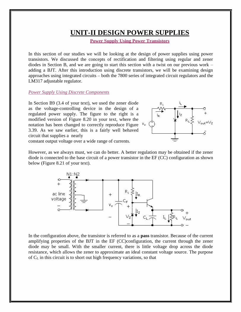
In Section B9 (3.4 of your text), we used the zener diode
as the voltage-controlling device in the design of a
regulated power supply. The figure to the right is a
modified version of Figure 8.20 in your text, where the
notation has been changed to correctly reproduce Figure
3.39. As we saw earlier, this is a fairly well behaved
circuit that supplies a nearly
constant output voltage over a wide range of currents.
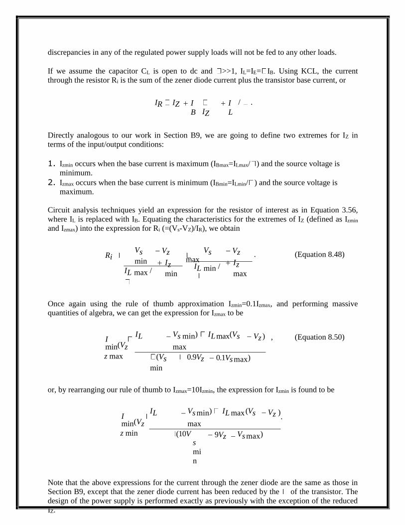
However, as we always must, we can do better. A better regulation may be obtained if the zener
diode is connected to the base circuit of a power transistor in the EF (CC) configuration as shown
below (Figure 8.21 of your text).
In the configuration above, the transistor is referred to as a pass transistor. Because of the current
amplifying properties of the BJT in the EF (CC)configuration, the current through the zener
diode may be small. With the smaller current, there is little voltage drop across the diode
resistance, which allows the zener to approximate an ideal constant voltage source. The purpose
of CL in this circuit is to short out high frequency variations, so that
discrepancies in any of the regulated power supply loads will not be fed to any other loads.
If we assume the capacitor CL is open to dc and >>1, IL=IE= IB. Using KCL, the current
through the resistor Ri is the sum of the zener diode current plus the transistor base current, or
IR IZ IB
IZ I
L / .
Directly analogous to our work in Section B9, we are going to define two extremes for IZ in
terms of the input/output conditions:
1. Izmin occurs when the base current is maximum (IBmax=ILmax/ ) and the source voltage is
minimum.
2. Izmax occurs when the base current is minimum (IBmin=ILmin/ ) and the source voltage is
maximum.
Circuit analysis techniques yield an expression for the resistor of interest as in Equation 3.56,
where IL is replaced with IB. Equating the characteristics for the extremes of IZ (defined as Izmin
and Izmax) into the expression for Ri (=(Vs-VZ)/IR), we obtain
Ri Vs
min
IL max /
Vz
Iz
min
Vs
max IL min /
Vz
Iz
max
. (Equation 8.48)
Once again using the rule of thumb approximation Izmin=0.1Izmax, and performing massive
quantities of algebra, we can get the expression for Izmax to be
I IL
min(Vz
Vs min) IL max(Vs
max
Vz ) , (Equation 8.50)
z max (Vs
min
0.9Vz 0.1Vs max)
or, by rearranging our rule of thumb to Izmax=10Izmin, the expression for Izmin is found to be
I IL
min(Vz
Vs min) IL max (Vs
max
Vz ) .
z min (10V
s
mi
n
9Vz Vs max)
Note that the above expressions for the current through the zener diode are the same as those in
Section B9, except that the zener diode current has been reduced by the of the transistor. The
design of the power supply is performed exactly as previously with the exception of the reduced
IZ.
p L
To estimate the capacitor CF, we determine the equivalent load seen by this capacitor. Assuming
the impedance of CL is very large for dc (ideally open), it may be neglected in the parallel
combination of ZCL||RL. This leaves us with the worst case situation of load resistance for the
equivalent load, or
RL (equivalent) RL (worst case) VS min
. (Equation 8.51) I L max
The expression of Equation 8.51 was defined as the worst case since it represents the smallest
load and, therefore, the largest load current. Substituting Equation 8.51 into Equation 3.62, we
get an expression for CF:
C Vs max
VZ
. (Equation 8.52)
F Vf R (equivalent)
Since the voltage gain of an EF (CC) amplifier may be approximated as unity, the output voltage
of the regulated power supply is
Vout
VE
VB VB
E
VZ VBE . (Equation 8.53, Modified)
If we assume that VBE remains constant, the percent regulation of this power supply is given by
%regulation VZ max
VZ
min * 100 RZ (IZ
max
IZ min) * 100 , (Equation 8.55)
VZ VZ
where VZ is the nominal zener voltage. The percent regulation has been significantly reduced by
using the BJT in the circuit since both IZmax and IZmin are divided by the of the transistor.
Power Supply Using IC Regulator (Three-Terminal Regulator)
The IC regulator further improves the performance of the zener diode regulator by incorporating
an operational amplifier. Using a single IC regulator and a few external components, excellent
regulation may be obtained, along with good stability and reliability and built-in overload
protection. In the following discussion, basic design considerations for IC regulators used in the
design of power supplies for low power applications will be presented.
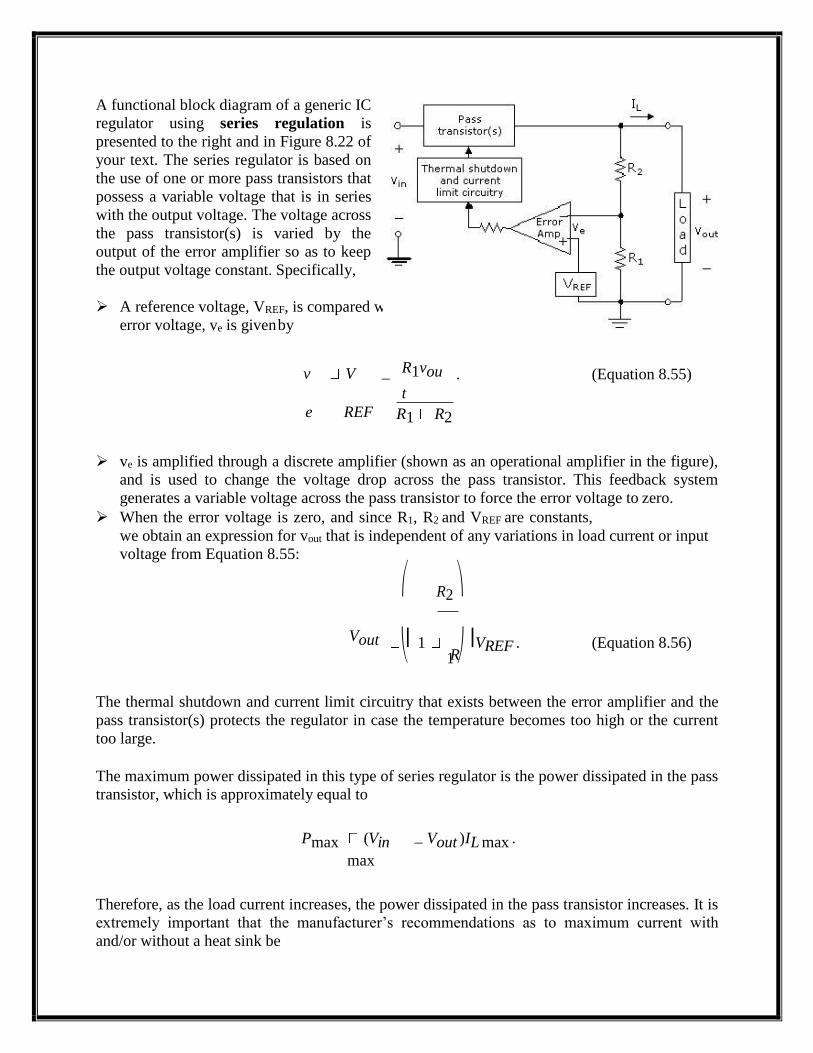
A functional block diagram of a generic IC
regulator using series regulation is
presented to the right and in Figure 8.22 of
your text. The series regulator is based on
the use of one or more pass transistors that
possess a variable voltage that is in series
with the output voltage. The voltage across
the pass transistor(s) is varied by the
output of the error amplifier so as to keep
the output voltage constant. Specifically,
A reference voltage, VREF, is compared with the voltage divided output, vout. The resulting
error voltage, ve is given by
v V R1vou
t
. (Equation 8.55)
e REF
R1 R2
ve is amplified through a discrete amplifier (shown as an operational amplifier in the figure),
and is used to change the voltage drop across the pass transistor. This feedback system
generates a variable voltage across the pass transistor to force the error voltage to zero.
When the error voltage is zero, and since R1, R2 and VREF are constants,
we obtain an expression for vout that is independent of any variations in load current or input
voltage from Equation 8.55:
⎛ R2 ⎞
Vout ⎜1
R ⎟VREF . (Equation 8.56)
⎝ 1 ⎠
The thermal shutdown and current limit circuitry that exists between the error amplifier and the
pass transistor(s) protects the regulator in case the temperature becomes too high or the current
too large.
The maximum power dissipated in this type of series regulator is the power dissipated in the pass
transistor, which is approximately equal to
Pmax (Vin
max
Vout )IL max .
Therefore, as the load current increases, the power dissipated in the pass transistor increases. It is
extremely important that the manufacturer’s recommendations as to maximum current with
and/or without a heat sink be
followed. Your text uses the example of an ILmax 0f 0.75A without a heat sink that may be
increased to 1.5A when the IC package is correctly secured to a heat sink.
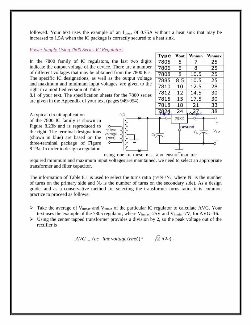
Power Supply Using 7800 Series IC Regulators
In the 7800 family of IC regulators, the last two digits
indicate the output voltage of the device. There are a number
of different voltages that may be obtained from the 7800 ICs.
The specific IC designations, as well as the output voltage
and maximum and minimum input voltages, are given to the
right in a modified version of Table
8.1 of your text. The specification sheets for the 7800 series
are given in the Appendix of your text (pages 949-954).
A typical circuit application
of the 7800 IC family is shown in
Figure 8.23b and is reproduced to
the right. The terminal designations
(shown in blue) are based on the
three-terminal package of Figure
8.23a. In order to design a regulator
using one of these ICs, and ensure that the
required minimum and maximum input voltages are maintained, we need to select an appropriate
transformer and filter capacitor.
The information of Table 8.1 is used to select the turns ratio (n=N1/N2, where N1 is the number
of turns on the primary side and N2 is the number of turns on the secondary side). As a design
guide, and as a conservative method for selecting the transformer turns ratio, it is common
practice to proceed as follows:
Take the average of Vinmax and Vinmin of the particular IC regulator to calculate AVG. Your
text uses the example of the 7805 regulator, where Vinmax=25V and Vinmin=7V, for AVG=16.
Using the center tapped transformer provides a division by 2, so the peak voltage out of the
rectifier is
AVG (ac line voltage (rms)) * /(2n) . 2
Type vout vinmin vinmax
7805 5 7 25
7806 6 8 25
7808 8 10.5 25
7885 8.5 10.5 25
7810 10 12.5 28
7812 12 14.5 30
7815 15 17.5 30
7818 18 21 33
7824 24 27 38
2
p
Once again, for the example using the 7805, if the rms value of the ac
line voltage is 115V, we get 115 / 2n 16 , or, n=5.
The filter capacitor is chosen to maintain the input voltage to the regulator as specified in
Table 8.1 by calculating
C Vmax ,
F Vf R
where
Vmax is the average of Vinmax and Vinmin from Table 8.1, V = Vmax-Vinmin
fp=120 for a 60Hz input (full wave recitification), and
RL=Vinmin/ILmax (or the worst case value).
According to the manufacturer’s data sheet, the capacitor at the output (CL) is not needed for
stability; however, it does improve the transient response of the regulator. It is further noted that
capacitance values of less than 0.1 F could cause instability. Your author states that CL should
be a high quality tantalum capacitor with a capacitance of 1.0 F, and should be connected close
to the 78XX regulator using short leads to improve the stability performance. Other possible
applications for the 78XX regulator are illustrated on page 953 of your text.
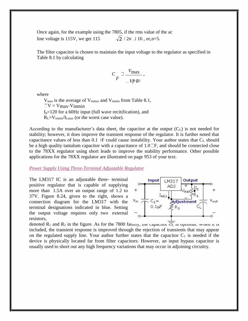
Power Supply Using Three-Terminal Adjustable Regulator
The LM317 IC is an adjustable three- terminal
positive regulator that is capable of supplying
more than 1.5A over an output range of 1.2 to
37V. Figure 8.24, given to the right, shows a
connection diagram for the LM317 with the
terminal designations indicated in blue. Setting
the output voltage requires only two external
resistors,
denoted R1 and R2 in the figure. As for the 7800 family, the capacitor CL is optional. When it is
included, the transient response is improved through the rejection of transients that may appear
on the regulated supply line. Your author further states that the capacitor C1 is needed if the
device is physically located far from filter capacitors. However, an input bypass capacitor is
usually used to short out any high frequency variations that may occur in adjoining circuitry.
L
The voltage, VREF, maintains a nominal 1.25V that is developed from a precision internal voltage
reference. VREF appears between the output and adjustment terminals and across the program
resistor, R1. Since VREF and R1 are constants, there is a constant current through R1 of
I1=VREF/R1. The output voltage is then given by
⎛ R2 ⎞
Vout
VREF
(I1
I ADJ )R2
VREF ⎜1 R
⎟ IADJR2 . (Equation 8.58)
⎝ 1 ⎠
The LM317 is packaged in a standard transistor package and provides both current limiting and thermal
overload protection. Your author states that both line and load regulations are better than in standard fixed
voltage regulators.
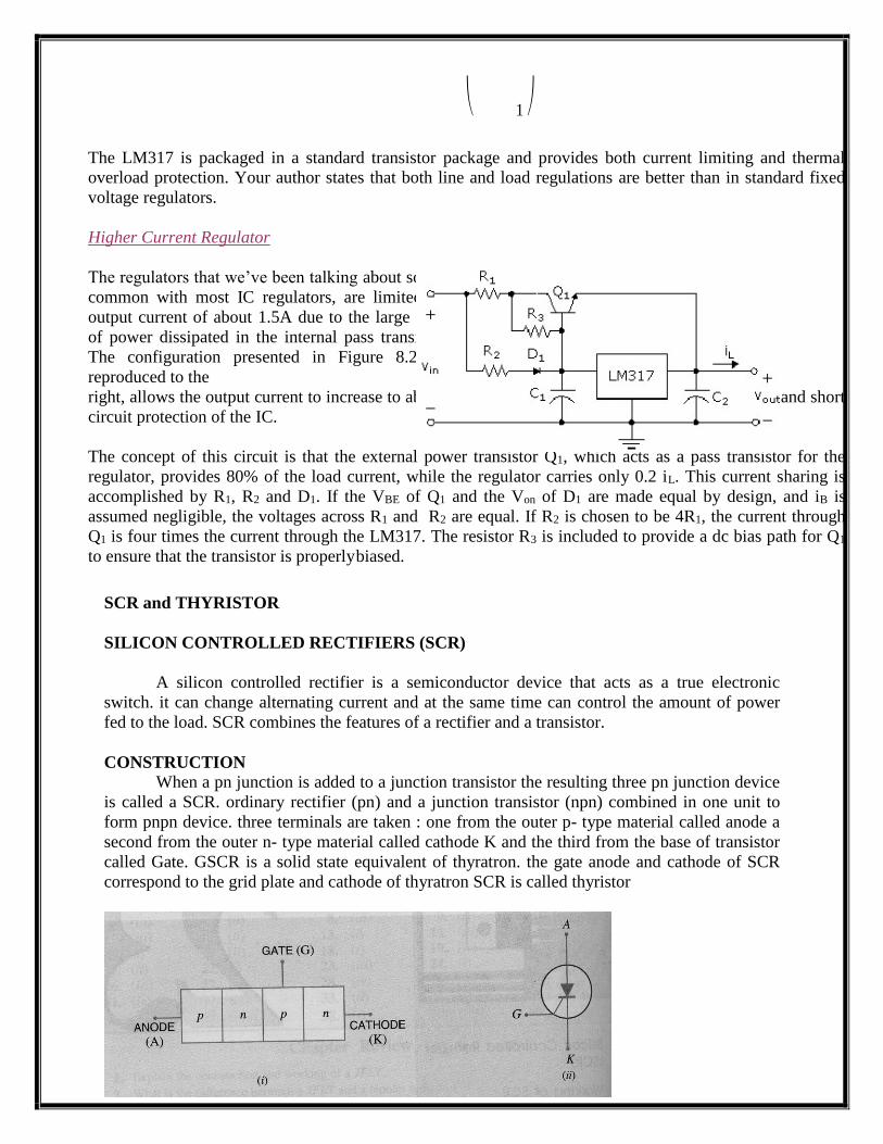
Higher Current Regulator
The regulators that we’ve been talking about so far, in
common with most IC regulators, are limited to an
output current of about 1.5A due to the large amount
of power dissipated in the internal pass transistor(s).
The configuration presented in Figure 8.25, and
reproduced to the
right, allows the output current to increase to about 5A while still preserving the thermal shutdown and short
circuit protection of the IC.
The concept of this circuit is that the external power transistor Q1, which acts as a pass transistor for the
regulator, provides 80% of the load current, while the regulator carries only 0.2 iL. This current sharing is
accomplished by R1, R2 and D1. If the VBE of Q1 and the Von of D1 are made equal by design, and iB is
assumed negligible, the voltages across R1 and R2 are equal. If R2 is chosen to be 4R1, the current through
Q1 is four times the current through the LM317. The resistor R3 is included to provide a dc bias path for Q1
to ensure that the transistor is properly biased.
SCR and THYRISTOR
SILICON CONTROLLED RECTIFIERS (SCR)
A silicon controlled rectifier is a semiconductor device that acts as a true electronic
switch. it can change alternating current and at the same time can control the amount of power
fed to the load. SCR combines the features of a rectifier and a transistor.
CONSTRUCTION
When a pn junction is added to a junction transistor the resulting three pn junction device
is called a SCR. ordinary rectifier (pn) and a junction transistor (npn) combined in one unit to
form pnpn device. three terminals are taken : one from the outer p type material called anode a
second from the outer n type material called cathode K and the third from the base of transistor
called Gate. GSCR is a solid state equivalent of thyratron. the gate anode and cathode of SCR
correspond to the grid plate and cathode of thyratron SCR is called thyristor
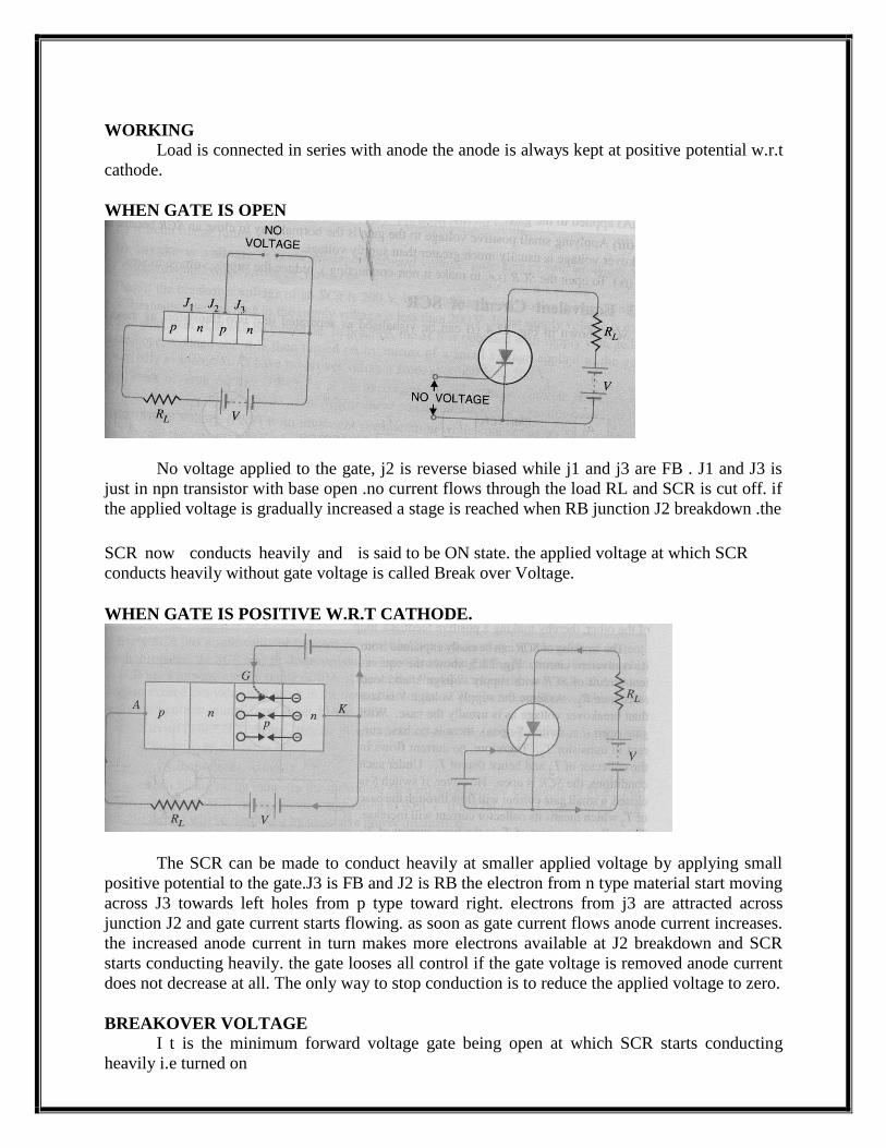
WORKING
Load is connected in series with anode the anode is always kept at positive potential w.r.t
cathode.
WHEN GATE IS OPEN
No voltage applied to the gate, j2 is reverse biased while j1 and j3 are FB . J1 and J3 is
just in npn transistor with base open .no current flows through the load RL and SCR is cut off. if
the applied voltage is gradually increased a stage is reached when RB junction J2 breakdown .the
SCR now conducts heavily and is said to be ON state. the applied voltage at which SCR
conducts heavily without gate voltage is called Break over Voltage.
WHEN GATE IS POSITIVE W.R.T CATHODE.
The SCR can be made to conduct heavily at smaller applied voltage by applying small
positive potential to the gate.J3 is FB and J2 is RB the electron from n type material start moving
across J3 towards left holes from p type toward right. electrons from j3 are attracted across
junction J2 and gate current starts flowing. as soon as gate current flows anode current increases.
the increased anode current in turn makes more electrons available at J2 breakdown and SCR
starts conducting heavily. the gate looses all control if the gate voltage is removed anode current
does not decrease at all. The only way to stop conduction is to reduce the applied voltage to zero.
BREAKOVER VOLTAGE
I t is the minimum forward voltage gate being open at which SCR starts conducting
heavily i.e turned on
PEAK REVERSE VOLTAGE( PRV)
It is the maximum reverse voltage applied to an SCR without conducting in the reverse
direction.
HOLDING CURRENT
It is the maximum anode current gate being open at which SCR is turned off from on
conditions.
FORWARD CURRENT RATING
It is the maximum anode current that an SCR is capable of passing without destruction
CIRCUIT FUSING RATING
It is the product of of square of forward surge current and the time of duration of the
surge
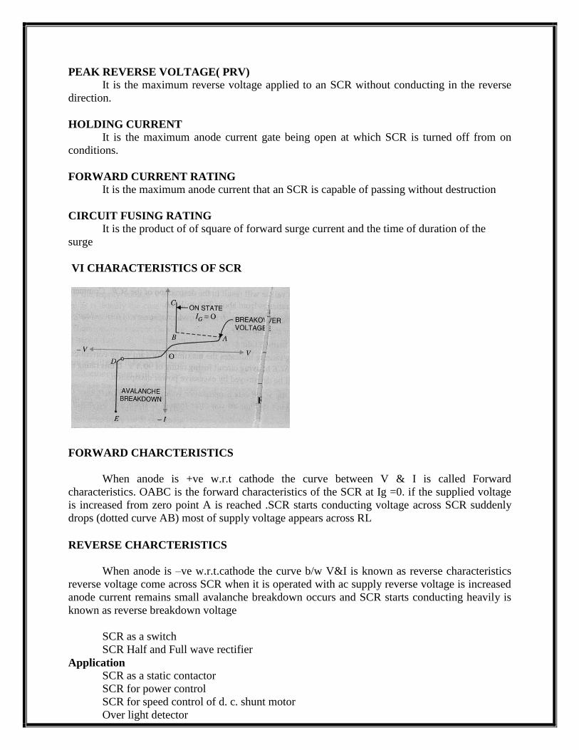
VI CHARACTERISTICS OF SCR
FORWARD CHARCTERISTICS
When anode is +ve w.r.t cathode the curve between V & I is called Forward
characteristics. OABC is the forward characteristics of the SCR at Ig =0. if the supplied voltage
is increased from zero point A is reached .SCR starts conducting voltage across SCR suddenly
drops (dotted curve AB) most of supply voltage appears across RL
REVERSE CHARCTERISTICS
When anode is –ve w.r.t.cathode the curve b/w V&I is known as reverse characteristics
reverse voltage come across SCR when it is operated with ac supply reverse voltage is increased
anode current remains small avalanche breakdown occurs and SCR starts conducting heavily is
known as reverse breakdown voltage
SCR as a switch
SCR Half and Full wave rectifier
Application
SCR as a static contactor
SCR for power control
SCR for speed control of d. c. shunt motor
Over light detector
Triggering (Turn on) Methods of Thyristor:
Triggering:
The turning on Process of the SCR is known as Triggering. In other words, turning the SCR from
ForwardBlocking state to ForwardConduction state is known as Triggering.The various
methods of SCR triggering are discussed here.
The various SCR triggering methods are
Forward Voltage Triggering
Thermal or Temperature Triggering
Radiation or Light triggering
dv/dt Triggering
Gate Triggering
(a) Forward Voltage Triggering:
In this mode, an additional forward voltage is applied between anode and cathode. When the anode terminal is positive with respect to cathode(VAK) , Junction J1 and J3 is
forward biased and junction J2 is reverse biased.
No current flows due to depletion region in J2 is reverse biased (except leakage current).
As VAK is further increased, at a voltage VBO (Forward Break Over Voltage) the
junction J2 undergoes avalanche breakdown and so a current flows and the device tends to turn ON(even when gate is open)
(b) Thermal (or) Temperature Triggering:
The width of depletion layer of SCR decreases with increase in junction temperature. Therefore in SCR when VAR is very near its breakdown voltage, the device is triggered
by increasing the junction temperature.
By increasing the junction temperature the reverse biased junction collapses thus the device starts to conduct.
(c) Radiation Triggering (or) Light Triggering:
For light triggered SCRs a special terminal niche is made inside the inner P layer instead of gate terminal.
When light is allowed to strike this terminal, free charge carriers are generated.
When intensity of light becomes more than a normal value, the thyristor starts conducting.
This type of SCRs are called as LASCR

(d) dv/dt Triggering:
When the device is forward biased, J1 and J3 are forward biased, J2 is reverse biased.
Junction J2 behaves as a capacitor, due to the charges existing across the junction.
If voltage across the device is V, the charge by Q and capacitance by C then, ic=dQ/dt
Q=CV ic=d(CV)/dt
C.dV/dt+V.dC/dt
as dC/dt = 0
ic = C.dV/dt
Therefore when the rate of change of voltage across the device becomes large, the device may turn ON, even if the voltage across the device is small.
(e) Gate Triggering:
This is most widely used SCR triggering method.
Applying a positive voltage between gate and cathode can Turn ON a
forward biased thyristor.
When a positive voltage is applied at the gate terminal, charge carriers are
injected in the inner Player, thereby reducing the depletion layer thickness.
As the applied voltage increases, the carrier injection increases, therefore the
voltage at which forward break over occurs decreases.

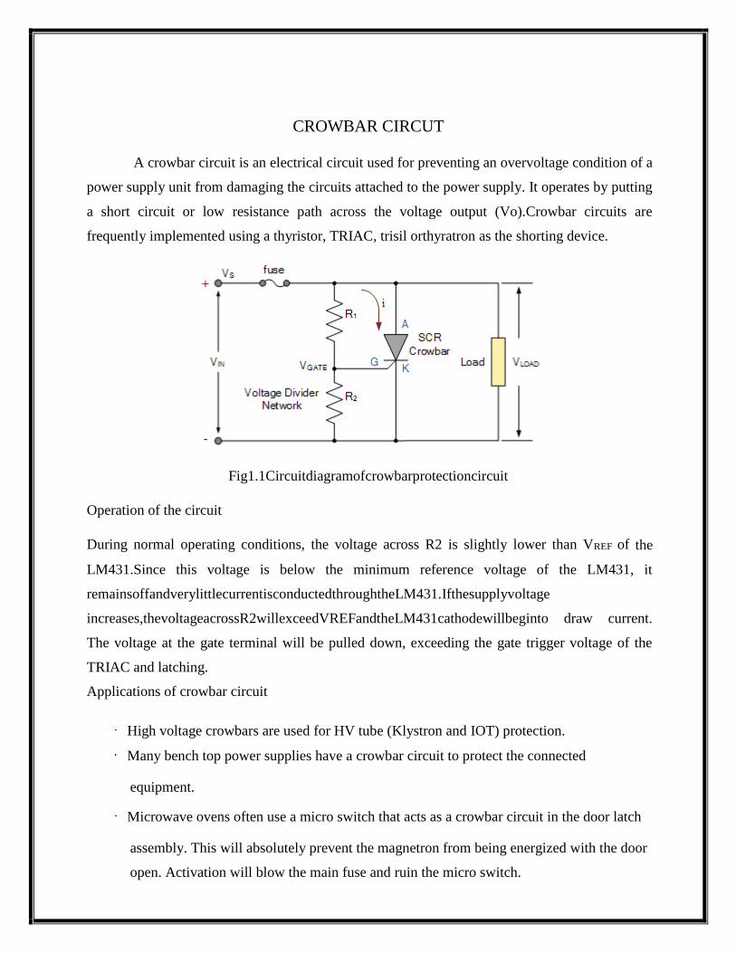
CROWBAR CIRCUT
A crowbar circuit is an electrical circuit used for preventing an overvoltage condition of a
power supply unit from damaging the circuits attached to the power supply. It operates by putting
a short circuit or low resistance path across the voltage output (Vo).Crowbar circuits are
frequently implemented using a thyristor, TRIAC, trisil orthyratron as the shorting device.
Fig1.1Circuitdiagramofcrowbarprotectioncircuit
Operation of the circuit
During normal operating conditions, the voltage across R2 is slightly lower than VREF of the
LM431.Since this voltage is below the minimum reference voltage of the LM431, it
remainsoffandverylittlecurrentisconductedthroughtheLM431.Ifthesupplyvoltage
increases,thevoltageacrossR2willexceedVREFandtheLM431cathodewillbeginto draw current.
The voltage at the gate terminal will be pulled down, exceeding the gate trigger voltage of the
TRIAC and latching.
Applications of crowbar circuit
High voltage crowbars are used for HV tube (Klystron and IOT) protection.
Many bench top power supplies have a crowbar circuit to protect the connected
equipment.
Microwave ovens often use a micro switch that acts as a crowbar circuit in the door latch
assembly. This will absolutely prevent the magnetron from being energized with the door
open. Activation will blow the main fuse and ruin the micro switch.
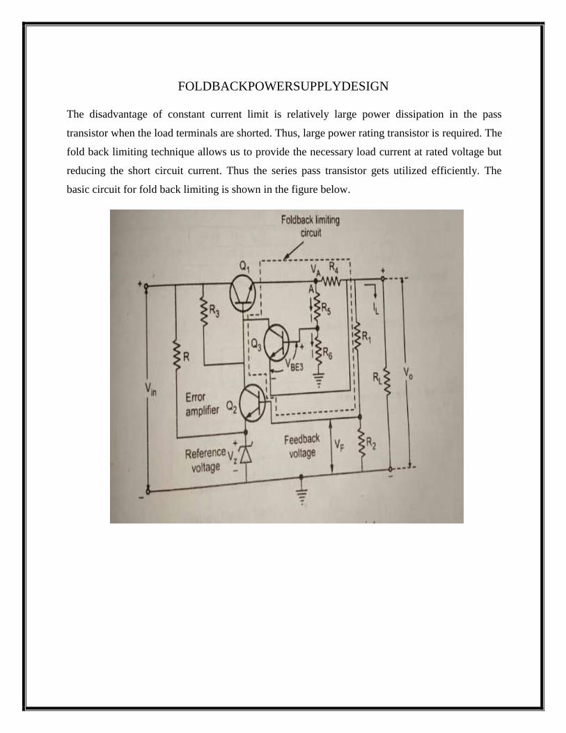
FOLDBACKPOWERSUPPLYDESIGN
The disadvantage of constant current limit is relatively large power dissipation in the pass
transistor when the load terminals are shorted. Thus, large power rating transistor is required. The
fold back limiting technique allows us to provide the necessary load current at rated voltage but
reducing the short circuit current. Thus the series pass transistor gets utilized efficiently. The
basic circuit for fold back limiting is shown in the figure below.
Circuit analysis
All the voltages at point AbeVAandthecurrentflowingthroungR4isalmostIL
VA=ILR4+Vo
NeglectingthebasecurrentflowingthroughR5andR6isthesameasI I=
VA
(R5+R6)
HencethevoltageatthebaseofQ3isthevoltageacrossR6
VB3= VA
.R6 R5+R6
R5+R6}
k= R6
R5+R6
VB3=k(ILR4+Vo)
ThevoltageacrosstheemitterofQ3is
VB=Vo
VBE3=VB-VE3
=kILR4+(k-1)Vo
IL=VBE3+ (1-k)Vo
kR4
Thusiftheoutputterminalsareshorted,theoutputvoltageVoreducestozero
Hence we get from the equation(6)
Isc=IL=VBE3/kR4
The rated current can be written as,
IL=Isc+ (1-k)Vo
{kR4}
IL =Rated load current
Isc=Short circuit current
The rated load current IL is also called Iknee known as knee current
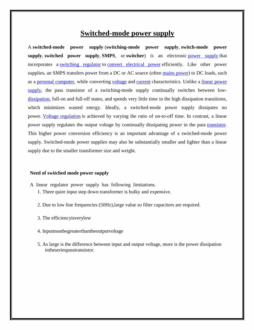
Switched-mode power supply
A switched-mode power supply (switching-mode power supply, switch-mode power
supply, switched power supply, SMPS, or switcher) is an electronic power supply that
incorporates a switching regulator to convert electrical power efficiently. Like other power
supplies, an SMPS transfers power from a DC or AC source (often mains power) to DC loads, such
as a personal computer, while converting voltage and current characteristics. Unlike a linear power
supply, the pass transistor of a switching-mode supply continually switches between low-
dissipation, full-on and full-off states, and spends very little time in the high dissipation transitions,
which minimizes wasted energy. Ideally, a switched-mode power supply dissipates no
power. Voltage regulation is achieved by varying the ratio of on-to-off time. In contrast, a linear
power supply regulates the output voltage by continually dissipating power in the pass transistor.
This higher power conversion efficiency is an important advantage of a switched-mode power
supply. Switched-mode power supplies may also be substantially smaller and lighter than a linear
supply due to the smaller transformer size and weight.
Need of switched mode power supply
A linear regulator power supply has following limitations.
1. There quire input step down transformer is bulky and expensive.
2. Due to low line frequencies (50Hz),large value so filter capacitors are required.
3. The efficiencyisverylow
4. Inputmustbegreaterthantheoutputvoltage
5. As large is the difference between input and output voltage, more is the power dissipation
intheseriespasstransistor.
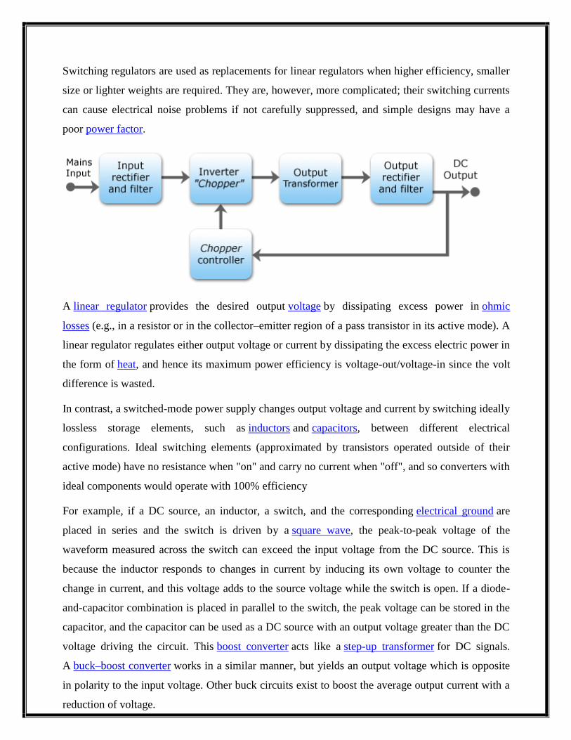
Switching regulators are used as replacements for linear regulators when higher efficiency, smaller
size or lighter weights are required. They are, however, more complicated; their switching currents
can cause electrical noise problems if not carefully suppressed, and simple designs may have a
poor power factor.
A linear regulator provides the desired output voltage by dissipating excess power in ohmic
losses (e.g., in a resistor or in the collector–emitter region of a pass transistor in its active mode). A
linear regulator regulates either output voltage or current by dissipating the excess electric power in
the form of heat, and hence its maximum power efficiency is voltage-out/voltage-in since the volt
difference is wasted.
In contrast, a switched-mode power supply changes output voltage and current by switching ideally
lossless storage elements, such as inductors and capacitors, between different electrical
configurations. Ideal switching elements (approximated by transistors operated outside of their
active mode) have no resistance when "on" and carry no current when "off", and so converters with
ideal components would operate with 100% efficiency
For example, if a DC source, an inductor, a switch, and the corresponding electrical ground are
placed in series and the switch is driven by a square wave, the peak-to-peak voltage of the
waveform measured across the switch can exceed the input voltage from the DC source. This is
because the inductor responds to changes in current by inducing its own voltage to counter the
change in current, and this voltage adds to the source voltage while the switch is open. If a diode-
and-capacitor combination is placed in parallel to the switch, the peak voltage can be stored in the
capacitor, and the capacitor can be used as a DC source with an output voltage greater than the DC
voltage driving the circuit. This boost converter acts like a step-up transformer for DC signals.
A buck–boost converter works in a similar manner, but yields an output voltage which is opposite
in polarity to the input voltage. Other buck circuits exist to boost the average output current with a
reduction of voltage.
In an SMPS, the output current flow depends on the input power signal, the storage elements and
circuit topologies used, and also on the pattern used (e.g., pulse-width modulation with an
adjustable duty cycle) to drive the switching elements. The spectral density of these switching
waveforms has energy concentrated at relatively high frequencies. As such, switching transients
and ripple introduced onto the output waveforms can be filtered with a small LC filter.
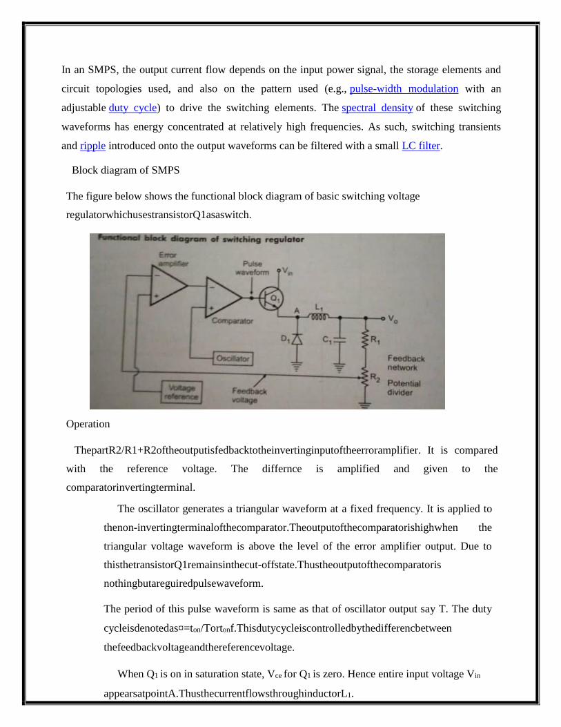
Block diagram of SMPS
The figure below shows the functional block diagram of basic switching voltage
regulatorwhichusestransistorQ1asaswitch.
Operation
ThepartR2/R1+R2oftheoutputisfedbacktotheinvertinginputoftheerroramplifier. It is compared
with the reference voltage. The differnce is amplified and given to the
comparatorinvertingterminal.
The oscillator generates a triangular waveform at a fixed frequency. It is applied to
thenon-invertingterminalofthecomparator.Theoutputofthecomparatorishighwhen the
triangular voltage waveform is above the level of the error amplifier output. Due to
thisthetransistorQ1remainsinthecut-offstate.Thustheoutputofthecomparatoris
nothingbutareguiredpulsewaveform.
The period of this pulse waveform is same as that of oscillator output say T. The duty
cycleisdenotedas¤=ton/Tortonf.Thisdutycycleiscontrolledbythedifferencbetween
thefeedbackvoltageandthereferencevoltage.
When Q1 is on in saturation state, Vce for Q1 is zero. Hence entire input voltage Vin
appearsatpointA.ThusthecurrentflowsthroughinductorL1.
WhenQ1 isoff,L1 stillcontinuetosupplycurrentthroughitselftotheload.Thediode
isprovidesthereturnpathforthecurrent.
The capacitor C1 acts to smooth out the voltage and the voltage at the output is
almost d.c in nature. The output voltage Vo of the switching regulator is a function of
dutycycleandtheinputvoltageVin.Mathematicallyitisexpressedas
Vo=to
n/T×
Vin
App
licat
ions
1.Indomesticproductslikecomput
ers
2.Inswitchedmodemobilephonecharg
er
3.UsedforDCtoDCconversion(inoutomobiles
)
4.Usedasextralow-
voltagesourceforlighting
Advantages and disadvantages
The main advantage of the switching power supply is greater efficiency than linear
regulators because the switching transistor dissipates little power when acting as a switch.
Other advantages include smaller size, low-noise, and lighter weight from the elimination
of heavy line-frequency transformers, and comparable heat generation. Standby power
loss is often much less than transformers.
Disadvantages include greater complexity, the generation of high-amplitude, high-
frequency energy that the low-pass filter must block to avoid electromagnetic
interference (EMI), a ripple voltage at the switching frequency and the harmonic
frequencies thereof.
Very low cost SMPSs may couple electrical switching noise back onto the mains power
line, causing interference with A/V equipment connected to the same phase. Non-power-
factor-corrected SMPSs also cause harmonic distortion.
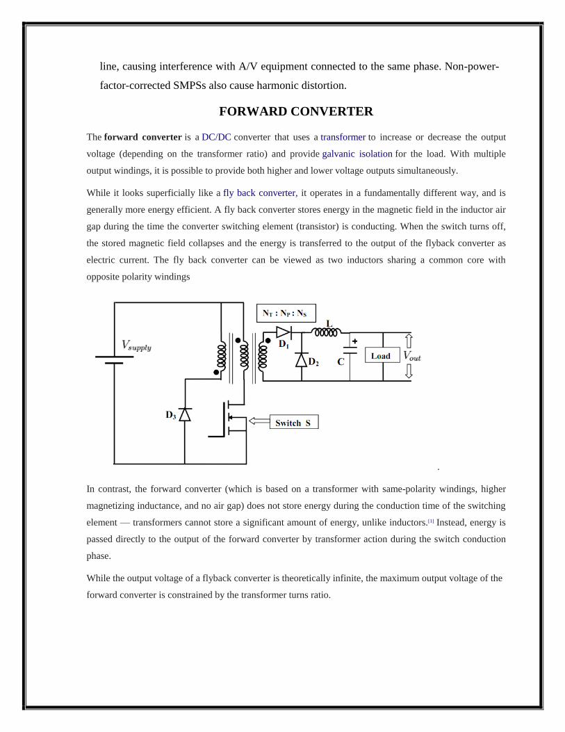
FORWARD CONVERTER
The forward converter is a DC/DC converter that uses a transformer to increase or decrease the output
voltage (depending on the transformer ratio) and provide galvanic isolation for the load. With multiple
output windings, it is possible to provide both higher and lower voltage outputs simultaneously.
While it looks superficially like a fly back converter, it operates in a fundamentally different way, and is
generally more energy efficient. A fly back converter stores energy in the magnetic field in the inductor air
gap during the time the converter switching element (transistor) is conducting. When the switch turns off,
the stored magnetic field collapses and the energy is transferred to the output of the flyback converter as
electric current. The fly back converter can be viewed as two inductors sharing a common core with
opposite polarity windings
.
In contrast, the forward converter (which is based on a transformer with same-polarity windings, higher
magnetizing inductance, and no air gap) does not store energy during the conduction time of the switching
element — transformers cannot store a significant amount of energy, unlike inductors.[1] Instead, energy is
passed directly to the output of the forward converter by transformer action during the switch conduction
phase.
While the output voltage of a flyback converter is theoretically infinite, the maximum output voltage of the
forward converter is constrained by the transformer turns ratio.
FLYBACK CONVERTER
The flyback converter is used in both AC/DC and DC/DC conversion with galvanic Isolation
between the input and any outputs. The flyback converters use galvanic Isolation because the
switch and the load are at different ground potentials. It is an effective way of breaking the
ground loops by preventing unwanted current from flowing between two units sharing a
ground conductor. It also prevents accidental current from reaching ground through a person’s
body. The galvanic Isolation can be done in various ways such as applying the use of
Transformer, Opto-isolator, Capacitor, Hall Effect, Magneto resistance and Relay. The
flyback converter is a buck-boost converter with the Inductor split to form a Transformer.
The flyback converter is an isolated power converter. The two prevailing control schemes are
voltage mode control and current mode control (in the majority of cases current mode control
needs to be dominant for stability during operation). Both require a signal related to the output
voltage. There are three common ways to generate this voltage. The first is to use an Opto-
coupler on the secondary circuitry to send a signal to the controller. The second is to wind a
separate winding on the coil and rely on the cross regulation of the design. The third consists
of sampling the voltage amplitude on the primary side, during the discharge, referenced to the
standing primary DC voltage.
A variation in primary-side sensing technology is where the output voltage and current are
regulated by monitoring the waveforms in the auxiliary winding used to power the Control IC
itself, which have improved the accuracy of both voltage and current regulation. The auxiliary
primary winding is used in the same discharge phase as the remaining secondary, but it builds
a rectified voltage referenced commonly with the primary DC, hence considered on the
primary side.
Previously, a measurement was taken across the whole of the flyback waveform which led to
error, but it was realized that measurements at the so-called knee point (when the secondary
current is zero, see Fig. 1) allow for a much more accurate measurement of what is happening
on the secondary side. This topology is now replacing ringing choke converters (RCCs) in
applications such as mobile phone chargers.
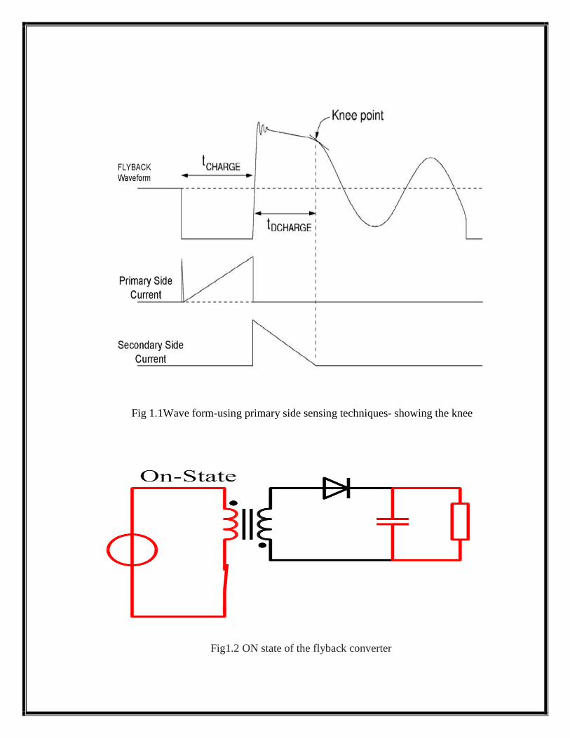
Fig 1.1Wave form-using primary side sensing techniques- showing the knee
Fig1.2 ON state of the flyback converter
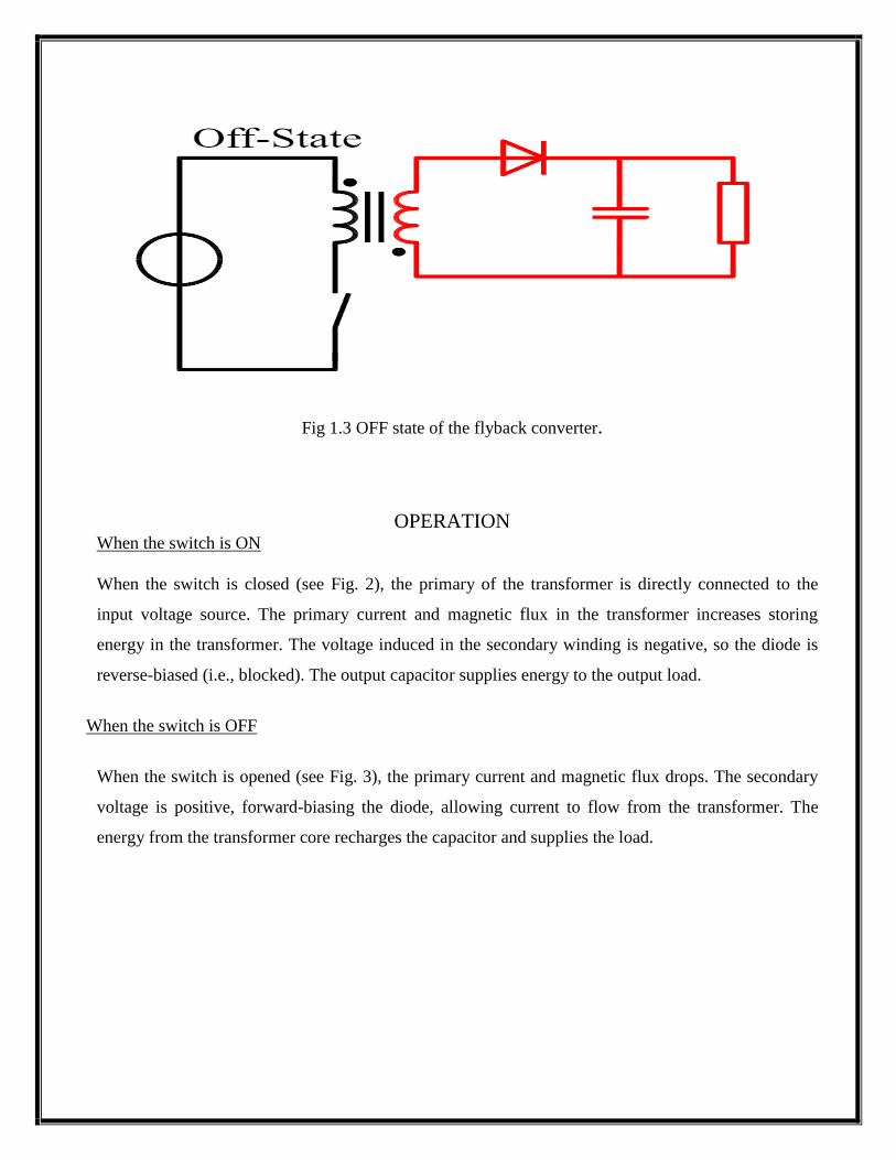
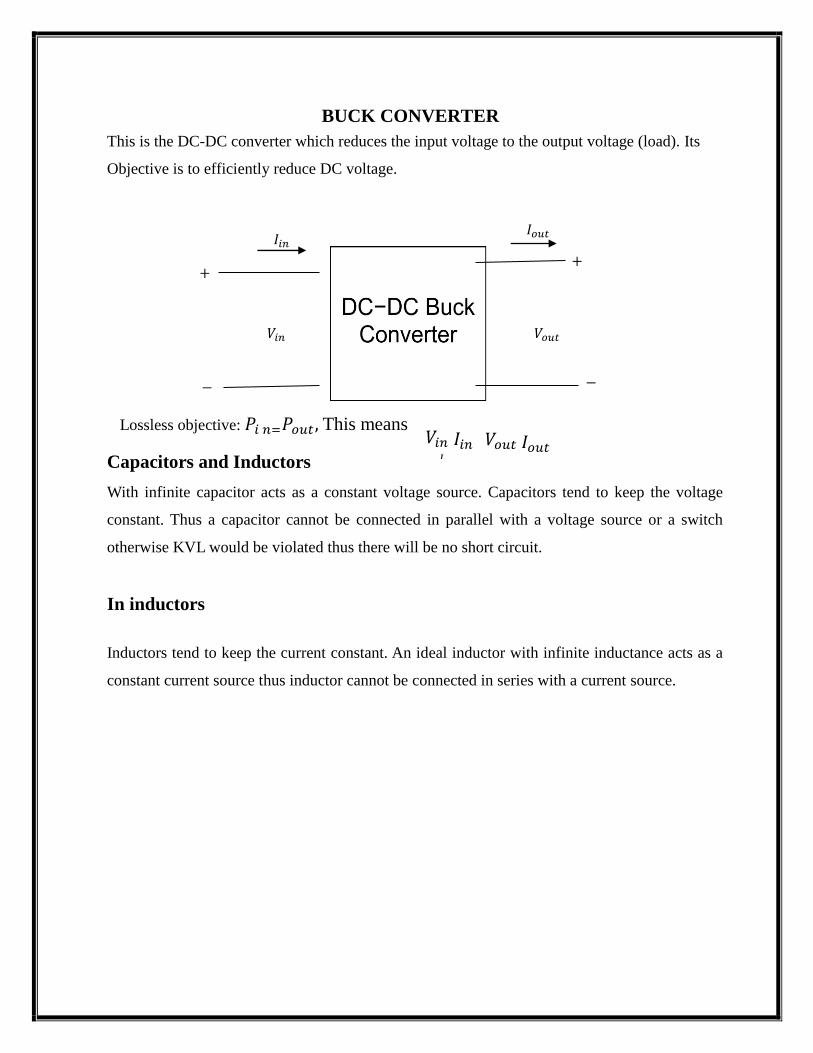
Fig 1.3 OFF state of the flyback converter.
OPERATION When the switch is ON
When the switch is closed (see Fig. 2), the primary of the transformer is directly connected to the
input voltage source. The primary current and magnetic flux in the transformer increases storing
energy in the transformer. The voltage induced in the secondary winding is negative, so the diode is
reverse-biased (i.e., blocked). The output capacitor supplies energy to the output load.
When the switch is OFF
When the switch is opened (see Fig. 3), the primary current and magnetic flux drops. The secondary
voltage is positive, forward-biasing the diode, allowing current to flow from the transformer. The
energy from the transformer core recharges the capacitor and supplies the load.
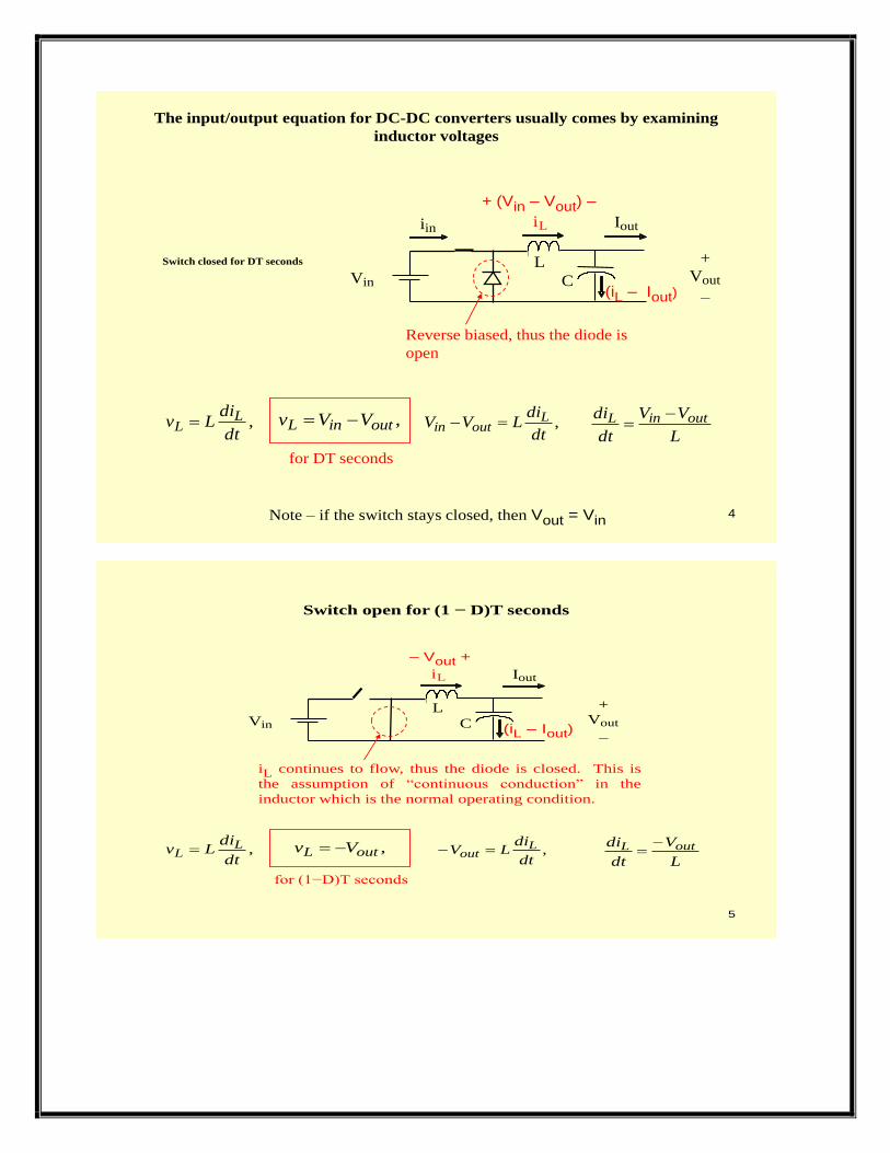
BUCK CONVERTER
This is the DC-DC converter which reduces the input voltage to the output voltage (load). Its
Objective is to efficiently reduce DC voltage.
Lossless objective: 𝑃𝑖 𝑛=𝑃𝑜𝑢𝑡 , This means
Capacitors and Inductors
With infinite capacitor acts as a constant voltage source. Capacitors tend to keep the voltage
constant. Thus a capacitor cannot be connected in parallel with a voltage source or a switch
otherwise KVL would be violated thus there will be no short circuit.
In inductors
Inductors tend to keep the current constant. An ideal inductor with infinite inductance acts as a
constant current source thus inductor cannot be connected in series with a current source.
𝑉𝑖𝑛 𝑉𝑜𝑢𝑡
𝐼𝑖𝑛 𝐼𝑜𝑢𝑡
+ +
− −
𝑉𝑖𝑛
𝐼𝑖𝑛
𝐼𝑖𝑛=
𝑉𝑜𝑢𝑡 𝐼𝑜𝑢𝑡
4
The input/output equation for DC-DC converters usually comes by examining
inductor voltages
Vin
+Vout
–
L
C
Ioutiin
+ (Vin – Vout) –
iL
(iL – Iout)
Reverse biased, thus the diode is
open
,dt
diLv L
L L
VV
dt
di outinL ,
dt
diLVV L
outin ,outinL VVv
for DT seconds
Note – if the switch stays closed, then Vout = Vin
Switch closed for DT seconds
5
Vin
+Vout
–
L
C
Iout
– Vout +
iL
(iL – Iout)
Switch open for (1 − D)T seconds
iL continues to flow, thus the diode is closed. This is
the assumption of “continuous conduction” in the
inductor which is the normal operating condition.
,dt
diLv L
L L
V
dt
di outL ,
dt
diLV L
out ,outL Vv
for (1−D)T seconds
6
Since the average voltage across L is zero
01 outoutinLavg VDVVDV
outoutoutin VDVVDDV
inout DVV
From power balance, outoutinin IVIV
D
II inout
, so
The input/output equation becomes
Note – even though iin is not constant (i.e., iinhas harmonics), the input power is still simply
Vin • Iin because Vin has no harmonics.
!
The input/ output equation can be found by the above equation formula which shows the input
voltage lower than the output voltage.
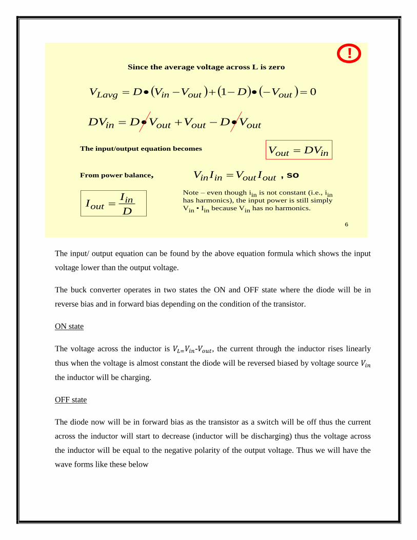
The buck converter operates in two states the ON and OFF state where the diode will be in
reverse bias and in forward bias depending on the condition of the transistor.
ON state
The voltage across the inductor is 𝑉𝐿=𝑉𝑖𝑛-𝑉𝑜𝑢𝑡, the current through the inductor rises linearly
thus when the voltage is almost constant the diode will be reversed biased by voltage source 𝑉𝑖𝑛
the inductor will be charging.
OFF state
The diode now will be in forward bias as the transistor as a switch will be off thus the current
across the inductor will start to decrease (inductor will be discharging) thus the voltage across
the inductor will be equal to the negative polarity of the output voltage. Thus we will have the
wave forms like these below
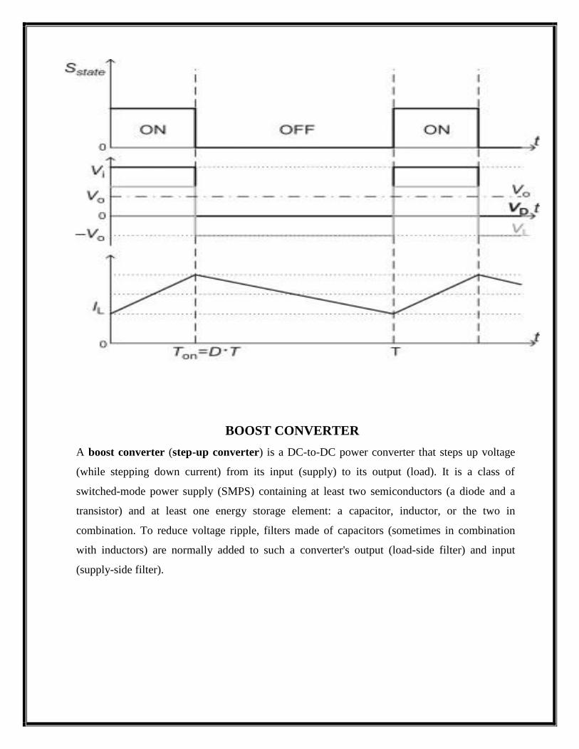
BOOST CONVERTER
A boost converter (step-up converter) is a DC-to-DC power converter that steps up voltage
(while stepping down current) from its input (supply) to its output (load). It is a class of
switched-mode power supply (SMPS) containing at least two semiconductors (a diode and a
transistor) and at least one energy storage element: a capacitor, inductor, or the two in
combination. To reduce voltage ripple, filters made of capacitors (sometimes in combination
with inductors) are normally added to such a converter's output (load-side filter) and input
(supply-side filter).
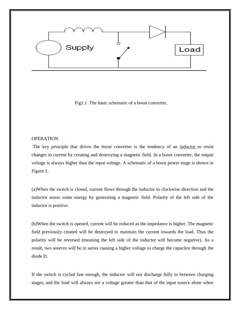
Fig1.1 The basic schematic of a boost converter.
OPERATION
The key principle that drives the boost converter is the tendency of an inductor to resist
changes in current by creating and destroying a magnetic field. In a boost converter, the output
voltage is always higher than the input voltage. A schematic of a boost power stage is shown in
Figure 1.
(a)When the switch is closed, current flows through the inductor in clockwise direction and the
inductor stores some energy by generating a magnetic field. Polarity of the left side of the
inductor is positive.
(b)When the switch is opened, current will be reduced as the impedance is higher. The magnetic
field previously created will be destroyed to maintain the current towards the load. Thus the
polarity will be reversed (meaning the left side of the inductor will become negative). As a
result, two sources will be in series causing a higher voltage to charge the capacitor through the
diode D.
If the switch is cycled fast enough, the inductor will not discharge fully in between charging
stages, and the load will always see a voltage greater than that of the input source alone when
the switch is opened. Also while the switch is opened, the capacitor in parallel with the load is
charged to this combined voltage. When the switch is then closed and the right hand side is
shorted out from the left hand side, the capacitor is therefore able to provide the voltage and
energy to the load. During this time, the blocking diode prevents the capacitor from discharging
through the switch. The switch must of course be opened again fast enough to prevent the
capacitor from discharging too much.
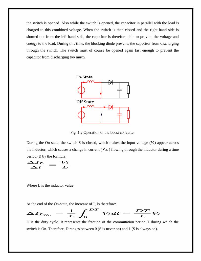
Fig 1.2 Operation of the boost converter
During the On-state, the switch S is closed, which makes the input voltage ( ) appear across
the inductor, which causes a change in current ( ) flowing through the inductor during a time
period (t) by the formula:
Where L is the inductor value.
At the end of the On-state, the increase of IL is therefore:
D is the duty cycle. It represents the fraction of the commutation period T during which the
switch is On. Therefore, D ranges between 0 (S is never on) and 1 (S is always on).
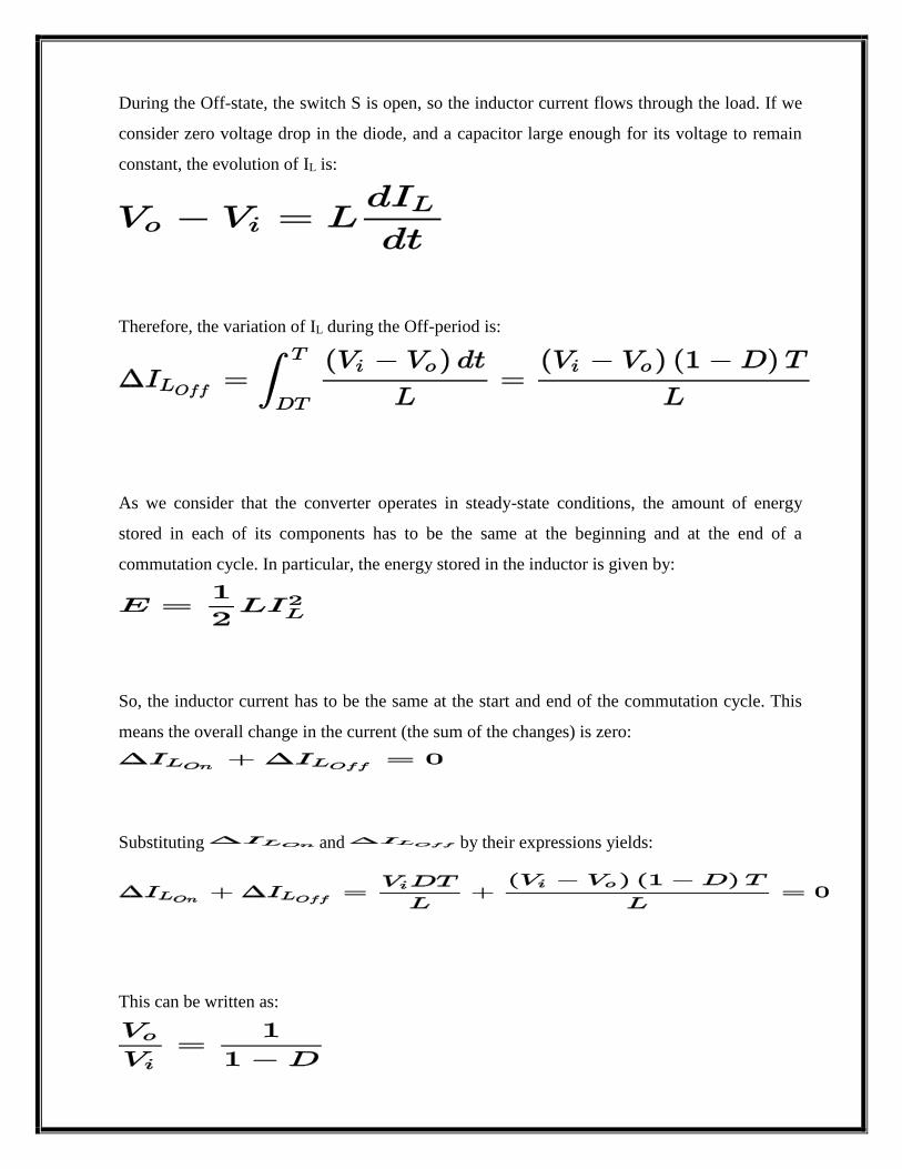
During the Off-state, the switch S is open, so the inductor current flows through the load. If we
consider zero voltage drop in the diode, and a capacitor large enough for its voltage to remain
constant, the evolution of IL is:
Therefore, the variation of IL during the Off-period is:
As we consider that the converter operates in steady-state conditions, the amount of energy
stored in each of its components has to be the same at the beginning and at the end of a
commutation cycle. In particular, the energy stored in the inductor is given by:
So, the inductor current has to be the same at the start and end of the commutation cycle. This
means the overall change in the current (the sum of the changes) is zero:
Substituting and by their expressions yields:
This can be written as:
The above equation shows that the output voltage is always higher than the input voltage (as the
duty cycle goes from 0 to 1), and that it increases with D, theoretically to infinity as D
approaches
1. This is why this converter is sometimes referred to as a step-up converter.
Rearranging the equation reveals the duty cycle to be:
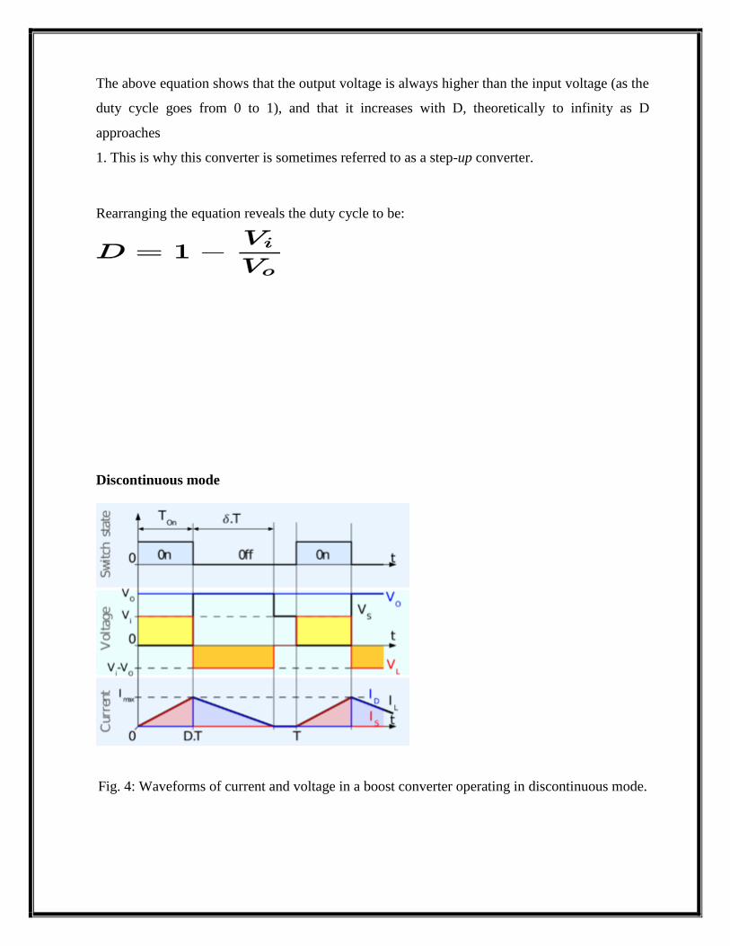
Discontinuous mode
Fig. 4: Waveforms of current and voltage in a boost converter operating in discontinuous mode.
If the ripple amplitude of the current is too high, the inductor may be completely discharged
before the end of a whole commutation cycle. This commonly occurs under light loads. In this
case, the current through the inductor falls to zero during part of the period (see waveforms in
figure 4). Although the difference is slight, it has a strong effect on the output voltage equation.
The voltage gain can be calculated as follows:
As the inductor current at the beginning of the cycle is zero, its maximum value
(at ) is
During the off-period, IL falls to zero after
:
Using the two previous equations, δ is:
The load current Io is equal to the average diode current (ID). As can be seen on figure 4, the
diode current is equal to the inductor current during the off-state. Therefore, the output current
can be written as:
Replacing ILmax and δ by their respective expressions yields:
Therefore, the output voltage gain can be written as follows:
Compared to the expression of the output voltage gain for continuous mode, this expression is
much more complicated. Furthermore, in discontinuous operation, the output voltage gain not
only depends on the duty cycle (D), but also on the inductor value (L), the input voltage (Vi),
the commutation period (T) and the output current (Io).
Substituting Io=Vo/R into the equation (R is the load), the output voltage gain can be rewritten
as:
Where
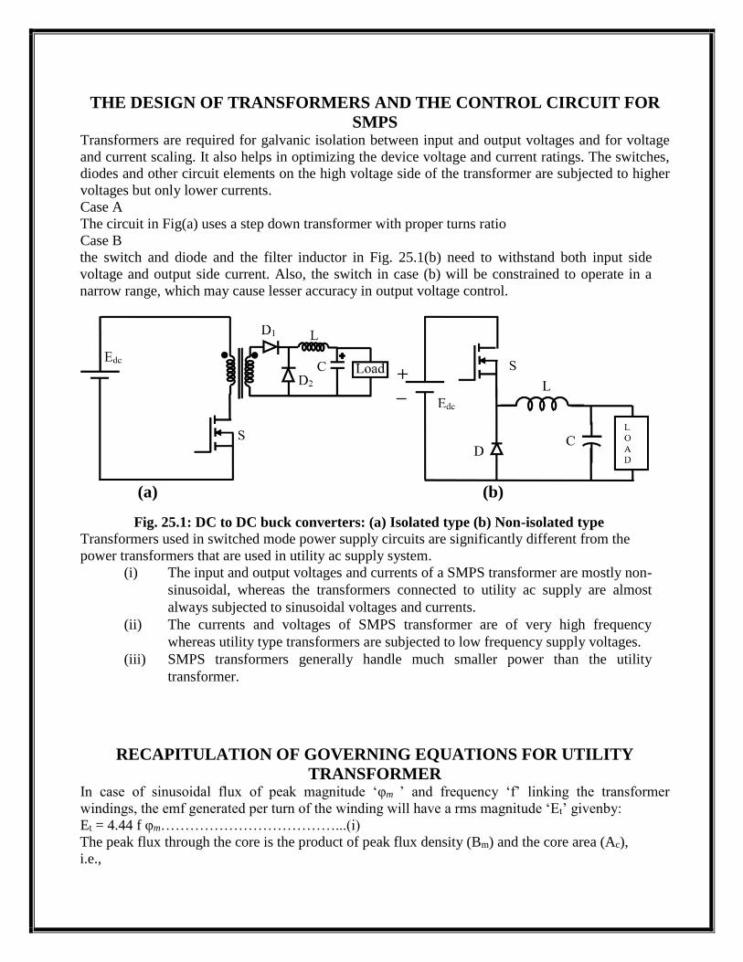
THE DESIGN OF TRANSFORMERS AND THE CONTROL CIRCUIT FOR
SMPS Transformers are required for galvanic isolation between input and output voltages and for voltage
and current scaling. It also helps in optimizing the device voltage and current ratings. The switches,
diodes and other circuit elements on the high voltage side of the transformer are subjected to higher
voltages but only lower currents.
Case A
The circuit in Fig(a) uses a step down transformer with proper turns ratio
Case B
the switch and diode and the filter inductor in Fig. 25.1(b) need to withstand both input side
voltage and output side current. Also, the switch in case (b) will be constrained to operate in a
narrow range, which may cause lesser accuracy in output voltage control.
(a) (b)
Fig. 25.1: DC to DC buck converters: (a) Isolated type (b) Non-isolated type Transformers used in switched mode power supply circuits are significantly different from the
power transformers that are used in utility ac supply system.
(i) The input and output voltages and currents of a SMPS transformer are mostly non-
sinusoidal, whereas the transformers connected to utility ac supply are almost
always subjected to sinusoidal voltages and currents.
(ii) The currents and voltages of SMPS transformer are of very high frequency
whereas utility type transformers are subjected to low frequency supply voltages.
(iii) SMPS transformers generally handle much smaller power than the utility
transformer.
RECAPITULATION OF GOVERNING EQUATIONS FOR UTILITY
TRANSFORMER In case of sinusoidal flux of peak magnitude ‘φm ’ and frequency ‘f’ linking the transformer
windings, the emf generated per turn of the winding will have a rms magnitude ‘Et’ givenby:
Et = 4.44 f φm………………………………...(i)
The peak flux through the core is the product of peak flux density (Bm) and the core area (Ac),
i.e.,
φm = Bm Ac …………………………………(ii)
The windings are placed around the core and are accommodated in the window of the
transformer. The transformer window area (Aw) is related with the winding’s current rating and
the number of turns. For a single-phase transformer the relation between them is given by:
Aw kwδ = 2 NI ………………………………. (iii)
, where kw is the window utilization factor and δ is the current density through the crosssectional
area of the transformer windings. Window utilization factor, roughly varies between 0.35 to 0.6
and is dependent on the insulation requirements of the windings. A typical figure for the current
density through copper conductors of naturally cooled transformers is 3X10⁶ amps per square
meter. The VA rating of a single phase transformer (= N Et I) can now be found from the above
equations as:
VA rating = 2.22 f Bm δ kw Ac Aw ----------------------------(iv)
For the given operating frequency (f) the product ‘Ac Aw’, known as area product is roughly
proportional to the VA rating of the transformer as other parameters have nearly fixed
magnitudes.
TRANSFORMER WITH SQUARE-WAVE VOLTAGE AND BIPOLAR FLUX
Determination of primary to secondary turns ratio (NP/ NS)
Let the input voltage vary from Vmin to Vmax. With minimum input voltage ‘Vmin’ and duty ratio
‘D’ = 0.5, the magnitude of square-shaped secondary side voltage should equal (Vo + VR), where
VR is the estimated voltage drop in the transformer winding, output rectifier and filter circuit
under maximum load condition. The transformer turns ratio can thus be estimated to
NP/ NS = Vmin/(Vo + VR)
Determination of peak magnitude of flux in the transformer core
The maximum flux in the core will correspond to a square wave voltage of magnitude Vmax
across the primary winding (refer to Figure with D=0.5). The frequency of voltage waveform
‘f’(=1/T) is same as the frequency at which the converter switches are turned on and is fixed
beforehand. Now by simple integration of the square wave voltage waveform, the peak flux ‘φm ’
is related to the input voltage as, Vmax = 4.0 f φm NP
Vmax = 4.0 f Bm Ac NP
Determination of winding current rating and requirement of window area
: Let ‘Iom’ be the peak expected load current
above and they carry the load (dc) current only in alternate half cycles. Thus the rms current
rating of each half equals Iom
√2 andthe net copper cross-sectional area required for the secondary
winding √2N IS om
δ.If the secondary was not center-tapped, the rectifier used would be bridge type
and the copper area for the secondary would have been just NsIom
δ .The primary side carries the
reflected secondary current.
The total window area requirement for the transformer can now be given as:
Aw kw= NsIom
δ(1+ √2)
where Aw is the window area and kw is the window utilization factor
Expression for VA rating of the transformer
VmaxNs
NPIom (1+ √2) = 4fBmδkw AcAw
Using relations derived above, Eqn. may be rewritten as:
V IomK1 K2(1+√2) = 4fBmδk Ac Aw
where K1 = Vmax
Vmin a factor allowing for input voltage variation and K2 =
(Vo + VR)
Vo
a factor coming due to voltage drop in rectifier diode, filter inductor etc. Vo Iom is the peak
output power from the SMPS.
Selection of transformer core and determination of number of turns in the windings:
Knowing the area product ‘Ac A w’, as given by Eqn.25.8, the appropriate transformer core is to be
selected from the core-manufacturer’s catalog. Once the area product matches, the details of other
dimensions of the transformer core are found from the catalog. Knowing window area (Aw) and
core area (Ac), the number of turns in the windings can be decided using Eqns. Like (25.5) or (25.6).
TRANSFORMER WITH UNIPOLAR FLUX
Many switched mode power supply circuits use only one controlled switch. The winding current and
core-flux for most of these transformers are unidirectional. when the forward converter switch is
turned on the primary winding is subjected to input dc voltage. As soon as the primary winding is
turned-off, the tertiary winding starts conducting and the voltage across primary goes negative with
a magnitude that equals the product of input voltage and the turns ratio between the primary and
tertiary windings. The maximum duty ratio (Dmax) of the switch is also limited by the turns ratio
between the primary and tertiary winding to allow resetting of the transformer flux. The maximum
input voltage (Vmax), switching frequency ‘f’(=1/T) and the maximum duty ratio (Dmax) are
related with the peak magnitude of core-flux is calculated as
Vmax Dmax = fφmNP= f Bm Ac NP
Because of unipolar nature of flux the utilization of core (in terms of emf generation) is poorer here.
The primary to secondary turns ratio (NP/ NS ) for the forward converter can be estimated as done
previously for the H-bridge converter. Accordingly, NP/ NS = Vmin Dmax /(Vo + VR).
The maximum rms current through the secondary winding can be equated to om max Iom√ Dmax and
the window area (Aw) requirement is given by
Aw kw = 2 Ns Iom√ Dmax
δ
Hence the VA ratings can be given as
V IomK1 K2(√Dmax) = 4fBmδk Ac Aw