Embed Size (px)
Citation preview

Published in IET Power ElectronicsReceived on 21st March 2012Revised on 11th July 2012doi: 10.1049/iet-pel.2012.0130
ISSN 1755-4535
Three-phase Z-source power supply designG.L. Calzo A. Lidozzi L. Solero F. CrescimbiniDepartment of Mechanical and Industrial Engineering, University of Roma Tre, Via della Vasca navale,79, 00146 Roma, ItalyE-mail: [email protected]
Abstract: Z-source converter configurations make it possible to overcome intrinsic limits present in conventional ac–dc anddc–ac converters. A typical three-phase inverter cannot supply output voltages greater than the voltages at its input; in thesame manner, a typical three-phase boost rectifier cannot supply output voltages lower than input voltages. Using Z-sourcetopology permits overcoming both these limits. In fact, a Z-source boost rectifier can theoretically either step-up or step-downthe output voltage to any desired value starting from the conventional three-phase diode bridge rectifier output voltage level.In addition, it presents intrinsic immunity to shoot-through states, resulting in improved reliability of the entire system. In thisstudy, attention is focused on the mathematical modelling of a three-phase Z-source boost rectifier for power factor correctionpower supply applications; using such a topology as first-stage converter allows designing the second-stage converters withthe same voltage constraints of single-phase units.
1 Introduction
For the present generation of three-phase power supplyconverters, the cost of the entire system is an importantissue to be considered during the design process alongsidethe overall performance. The front-end converter for powersupply applications must achieve a high-power factor, low-harmonic distortion, high efficiency, high reliability andlow electromagnetic interference noise. One of theconventional practices, commonly used to obtain three-phase power supply converters, is the use of a two-stageapproach based on single-phase power modules [1], thefirst stage of each module is used to perform the powerfactor correction (PFC) function to meet harmonic currentstandards such as the IEC 61000-3-2, whereas the second-stage dc–dc converter regulates the dc output voltage ofthe system and guarantees system current sharing. Usually,for proper operation of a two-stage power supply, theintermediate bus voltage must be slightly higher than twicethe input phase peak voltage, which means that the voltagerating of the boost power switches must be at least 700 Vin applications for which the rated line-to-line inputvoltage is 400 V. Same requirement for the intermediatebus voltage is expected in three-phase boost rectifiers. As aconsequence, the switches of the second-stage dc–dcconverter will experience high-voltage stress, unless athree-level structure is used for the dc–dc converter [2–5].A significant breakthrough in simplifying the single-phasemodules was achieved by some rectifiers [6, 7]. TheVIENNA rectifier can be seen as a simplified version ofthree single-phase PFCs connected to the sameintermediate bus voltage.
The Z-source topology can be proposed as the first stageof a three-phase PFC in order to reduce the dc-link voltage
down to 400 V; as a consequence same design of single-phase PFC second stage can also be used for three-phaseapplications where parallel connection of two or moresecond stage units can be used at the occurrence, thusreducing design, manufacturing and maintenance costs.Same benefits can be achieved when the proposed three-phase Z-source boost rectifier is applied to distributedgeneration systems where either photovoltaic, wind ordiesel generation units are considered [8, 9]. The Z-sourceconfiguration has no cost advantages when compared withthe conventional three-phase boost rectifier; in fact, theadditional Z-section components represent an additionalcost, whereas the input filters as well as the switchingcomponents have the same size and cost of conventionalconfiguration [10]. However, the opportunity of 400Vdc asdc-link voltage even with three-phase line-to-line 400Vac
power supply grid is highly valued when second-stagepower electronic units are required as in telecomapplications and in auxiliary dc power supply systems ingeneral.
The paper presents the modelling of a 10 kW rated three-phase Z-source boost rectifier, which is intended to operateas the first stage of a two-stage PFC power supply. Thecontrol transfer functions are derived in both steady stateand dynamic state. Furthermore, the influences of maincircuital parameters on system dynamics are described. Themain criteria for the Z-source boost rectifier input filterdesign are discussed, as well as a design algorithm isproposed for the Z-section LC components The controltransfer functions are then used to design regulators of thecontrol loops, a prototype of the converter has been builtand the experimental results are discussed with reference tothe benchmark configuration of PFC three-phase boostrectifier and dc–dc buck converter.
IET Power Electron., pp. 1–12 1doi: 10.1049/iet-pel.2012.0130 & The Institution of Engineering and Technology 2012
www.ietdl.org
2 Three-phase Z-source boost rectifiermodelling
2.1 Steady state
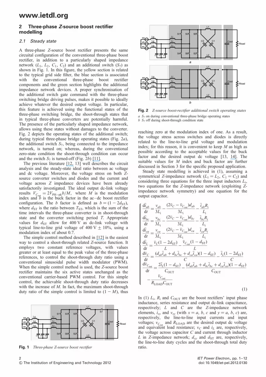
A three-phase Z-source boost rectifier presents the samecircuital configuration of the conventional three-phase boostrectifier, in addition to a particularly shaped impedancenetwork (L1, L2, C1, C2) and an additional switch (S7) asshown in Fig. 1. In this figure, the yellow section is relatedto the typical grid side filter, the blue section is associatedwith the conventional three-phase boost rectifiercomponents and the green section highlights the additionalimpedance network devices. A proper synchronisation ofthe additional switch gate command with the three-phaseswitching bridge driving pulses, makes it possible to ideallyachieve whatever the desired output voltage. In particular,this feature is achieved using the functional states of thethree-phase switching bridge, the shoot-through states thatin typical three-phase converters are potentially harmful.The presence of the particularly shaped impedance network,allows using these states without damages to the converter.Fig. 2 depicts the operating states of the additional switch;during typical three-phase bridge operating states (Fig. 2a),the additional switch S7, being connected to the impedancenetwork, is turned on; whereas, during the conventionalzero-state condition the shoot-through condition can occurand the switch S7 is turned-off (Fig. 2b) [11].
The previous literature [12, 13] well describes the circuitanalysis and the steady-state ideal ratio between ac voltageand dc voltage. Moreover, the voltage stress on both Z-source converter switches and diodes and the current andvoltage across Z impedance devices have been alreadysatisfactorily investigated. The ideal output dc-link voltageresults VCout
= 2VPH−pkb/M , where M is the modulationindex and b is the buck factor in the ac–dc boost rectifierconfiguration. The b factor is defined as b ¼ (1 2 2dST),where dST is the ratio between TST, which is the sum of thetime intervals the three-phase converter is in shoot-throughstate and the converter switching period T. Appropriatevalues for dST allow for 400 V as dc-link voltage withtypical line-to-line grid voltage of 400 V + 10%, using amodulation index of about 0.7.
The simple control method described in [12] is the easiestway to control a shoot-through related Z-source function. Itemploys two constant reference voltages, with valuesgreater or at least equal to the peak value of the three-phasereferences, to control the shoot-through duty ratio using aconventional sinusoidal pulse width modulator (PWM).When the simple control method is used, the Z-source boostrectifier maintains the six active states unchanged as theconventional carrier-based PWM control. For this simplecontrol, the achievable shoot-through duty ratio decreaseswith the increase of M. In fact, the maximum shoot-throughduty ratio of the simple control is limited to (1 2 M ), thus
reaching zero at the modulation index of one. As a result,the voltage stress across switches and diodes is directlyrelated to the line-to-line grid voltage and modulationindex; for this reason, it is convenient to keep M as high aspossible according to the acceptable values for the buckfactor and the desired output dc voltage [13, 14]. Thesuitable values for M index and buck factor are furtherdiscussed in Section 3 for the specific proposed application.
Steady state modelling is achieved in (1), assuming asymmetrical Z-impedance network (L1 ¼ L2, C1 ¼ C2) andconsidering three equations for the three input inductors Li,two equations for the Z-impedance network (exploiting Z-impedance network symmetry) and one equation for theoutput capacitor.
d�iab
dt= vab
3Li
−(2�vC − �vCout
)dab
3Li
−�iabRi
Li
d�ibc
dt= vbc
3Li
−(2�vC − �vCout
)dbc
3Li
−�ibcRi
Li
d�ica
dt= vca
3Li
−(2�vC − �vCout
)dca
3Li
−�icaRi
Li
d�iLdt
= �vC(1 − 2dST)
L−�vCout
(1 − dST)
Ld�vC
dt= (dab
�iab + dbc�ibc + dca
�ica)(1 − dST)
C−�iL(1 − 2dST)
Cd�vCout
dt= 2�iL(1 − dST)
COUT
− (dab�iab + dbc
�ibc + dca�ica)(1 − dST)
COUT
−�vCout
RLOADCOUT
⎧⎪⎪⎪⎪⎪⎪⎪⎪⎪⎪⎪⎪⎪⎪⎪⎪⎪⎪⎪⎪⎪⎪⎪⎪⎪⎨⎪⎪⎪⎪⎪⎪⎪⎪⎪⎪⎪⎪⎪⎪⎪⎪⎪⎪⎪⎪⎪⎪⎪⎪⎪⎩
(1)
In (1) Li, Ri and COUT are the boost rectifiers’ input phaseinductance, series resistance and output dc-link capacitance,respectively; L and C are the Z-impedance networkelements, ixy and vxy (with x ¼ a, b, c and y ¼ a, b, c) are,respectively, the line-to-line input currents and inputvoltages; vCout
and RLOAD are the desired output dc voltageand equivalent load resistance; vC and iL are, respectively,the voltage across capacitor C and current through inductorL in Z-impedance network; dxy and dST are, respectively,the line-to-line duty cycles and the shoot-through total dutyratio.Fig. 1 Three-phase Z-source boost rectifier
Fig. 2 Z-source boost-rectifier additional switch operating states
a S7 on during conventional three-phase bridge operating statesb S7 off during shoot-through condition state
2 IET Power Electron., pp. 1–12
& The Institution of Engineering and Technology 2012 doi: 10.1049/iet-pel.2012.0130
www.ietdl.org
The grid side filter does not significantly affect the controllaw behaviour, when it is sized with high-frequencyresonance with respect to the control bandwidth as shownalso in Section 3. The final purpose of modelling is todefine the transfer function expressions, which are useful toderive recommendations for sizing the control laws of theinvestigated power supply system. For this reason, theconverter modelling is achieved here by neglecting the gridside filter contribution. The obtained sixth grade system isfurther simplified, when Park’s transformation is applied tothe three-phase voltages and currents system at the input ofthe converter, thus leading to the state space matrixrepresentations (2).
2.2 Dynamic modelling
Dynamic modelling of the three-phase Z-source boost rectifieris achieved by means of the procedure of linearisation andperturbation of (2) [15–19]; the result of the process isrepresented by (3) and further manipulations allow us towrite all the transfer function expressions in a dynamicstate, which are useful for sizing the control laws of theinvestigated power supply system. In (3), the changes instate variables are expressed in terms of changes in inputvoltages, control signals, operating point and the circuitalparameters. The transfer function for the control design of
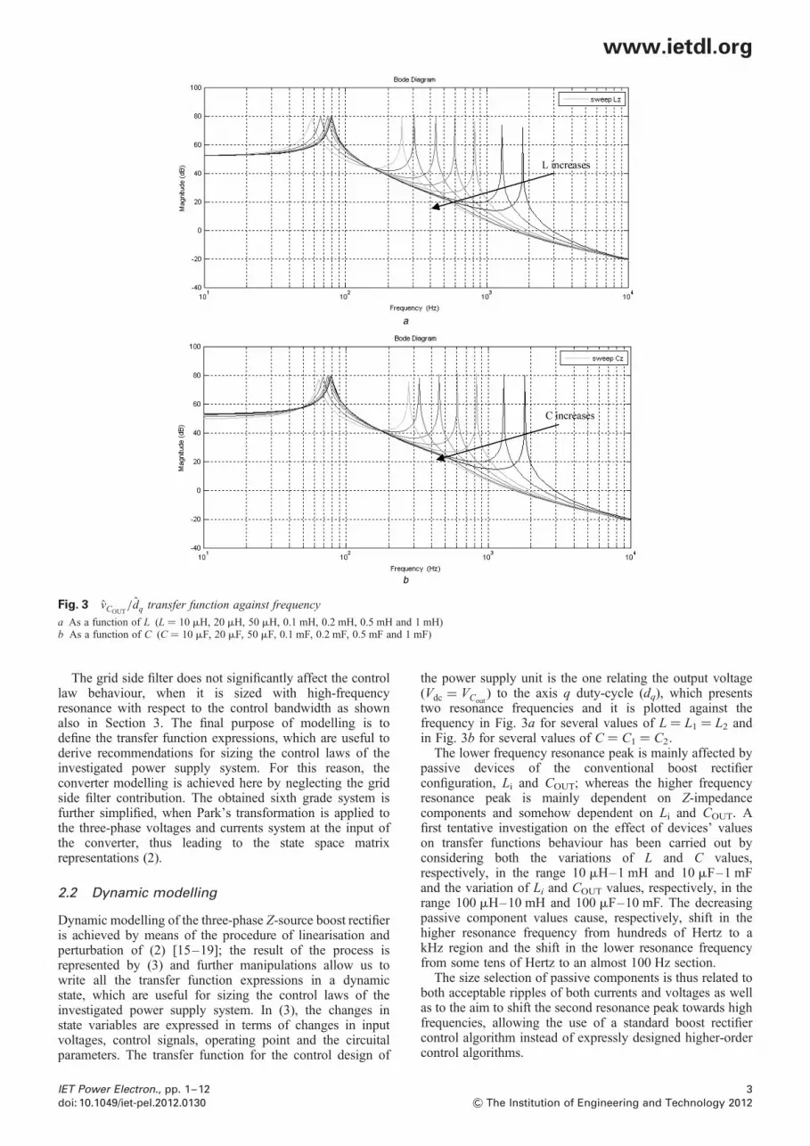
the power supply unit is the one relating the output voltage(Vdc = VCout
) to the axis q duty-cycle (dq), which presentstwo resonance frequencies and it is plotted against thefrequency in Fig. 3a for several values of L ¼ L1 ¼ L2 andin Fig. 3b for several values of C ¼ C1 ¼ C2.
The lower frequency resonance peak is mainly affected bypassive devices of the conventional boost rectifierconfiguration, Li and COUT; whereas the higher frequencyresonance peak is mainly dependent on Z-impedancecomponents and somehow dependent on Li and COUT. Afirst tentative investigation on the effect of devices’ valueson transfer functions behaviour has been carried out byconsidering both the variations of L and C values,respectively, in the range 10 mH–1 mH and 10 mF–1 mFand the variation of Li and COUT values, respectively, in therange 100 mH–10 mH and 100 mF–10 mF. The decreasingpassive component values cause, respectively, shift in thehigher resonance frequency from hundreds of Hertz to akHz region and the shift in the lower resonance frequencyfrom some tens of Hertz to an almost 100 Hz section.
The size selection of passive components is thus related toboth acceptable ripples of both currents and voltages as wellas to the aim to shift the second resonance peak towards highfrequencies, allowing the use of a standard boost rectifiercontrol algorithm instead of expressly designed higher-ordercontrol algorithms.
Fig. 3 vCOUT/dq transfer function against frequency
a As a function of L (L ¼ 10 mH, 20 mH, 50 mH, 0.1 mH, 0.2 mH, 0.5 mH and 1 mH)b As a function of C (C ¼ 10 mF, 20 mF, 50 mF, 0.1 mF, 0.2 mF, 0.5 mF and 1 mF)
IET Power Electron., pp. 1–12 3doi: 10.1049/iet-pel.2012.0130 & The Institution of Engineering and Technology 2012
www.ietdl.org
The boost-rectifier input filter is mainly sized to ensure theinternational standard on current total harmonic distortion(THD) with respect to the maximum current ripple; whereas,the output capacitance is mainly related to the maximumacceptable dc-link voltage ripple as well as to the maximumdc-link capacitors’ root-mean-square (RMS) current ripple.As a consequence, the lower order resonance of theconverter transfer function is the result of the aboveconsiderations and, as a second step, its consistency isusually verified with both the grid fundamental frequencyand the converter switching frequency.
The Z-impedance inductors are sized on the basis of theestablished current ripple value and the desired load powerrange in continuous conduction mode (CCM) of operation.As a result, the position of the converter transfer function
higher-order resonance is basically related to theZ-impedance capacitor’s selection. (see (2) and (3))
3 LC components selection criteria
In this section, the design criteria for both the converter inputfilter LC components and Z-impedance LC components arediscussed in relation to the specific proposed application.The main characteristics of the three-phase Z-source boostrectifier converter are listed in Table 1.
The converter input and output voltage level specificationsdefine the satisfactory combinations of the modulation indexand buck factor values; in fact, with the simple controlmethod, the achievable shoot-through duty ratio decreases
d
dt
�id�iq�iL�vC
�vCout
⎡⎢⎢⎢⎢⎢⎢⎣
⎤⎥⎥⎥⎥⎥⎥⎦
=
k1 v 0 −2ddk2 ddk2
−v k1 0 −2dqk2 dqk2
0 0 0 k5/L −k4/L
ddk3/C dqk3/C −k5/C 0 0
−ddk3/COUT −dqk3/COUT 2k4/COUT 0 −1/(RLOADCOUT)
⎡⎢⎢⎢⎢⎢⎢⎣
⎤⎥⎥⎥⎥⎥⎥⎦
×
�id�iq�iL�vC
�vCout
⎡⎢⎢⎢⎢⎢⎢⎣
⎤⎥⎥⎥⎥⎥⎥⎦+
k2 0
0 k2
0 0
0 0
0 0
⎡⎢⎢⎢⎢⎢⎢⎣
⎤⎥⎥⎥⎥⎥⎥⎦
�vd
�vq
[ ]�id�iq�iL�vC
�vCout
�iLOAD
⎡⎢⎢⎢⎢⎢⎢⎢⎢⎣
⎤⎥⎥⎥⎥⎥⎥⎥⎥⎦
=
1 0 0 0 0
0 1 0 0 0
0 0 1 0 0
0 0 0 1 0
0 0 0 0 1
0 0 0 01
RLOAD
⎡⎢⎢⎢⎢⎢⎢⎢⎢⎢⎢⎣
⎤⎥⎥⎥⎥⎥⎥⎥⎥⎥⎥⎦
�id�iq�iL�vC
�vCout
⎡⎢⎢⎢⎢⎢⎢⎣
⎤⎥⎥⎥⎥⎥⎥⎦+
0 0
0 0
0 0
0 0
0 0
0 0
⎡⎢⎢⎢⎢⎢⎢⎢⎢⎣
⎤⎥⎥⎥⎥⎥⎥⎥⎥⎦
�vd
�vq
[ ]where
k1 = −Ri
Li
k2 = 1
3Li
k3 = 3
2(1 − dST)
k4 = (1 − dST) k5 = (1 − 2dST)
(2)
d
dt
idiq
iLvC
vCout
⎡⎢⎢⎢⎢⎢⎢⎣
⎤⎥⎥⎥⎥⎥⎥⎦
=
k1 v 0 −2Ddk2 Ddk2
−v k1 0 −2Dqk2 Dqk2
0 0 0 k4/L −k5/L
k3Dd/C k3Dq/C −k4/C 0 0
−k3Dd/COUT −k3Dq/COUT 2k5/COUT 0 −1/(COUTRLOAD)
⎡⎢⎢⎢⎢⎢⎢⎣
⎤⎥⎥⎥⎥⎥⎥⎦
×
idiq
iLvC
vCout
⎡⎢⎢⎢⎢⎢⎢⎣
⎤⎥⎥⎥⎥⎥⎥⎦+
k6 0 0 k2 0
0 k6 0 0 k2
0 0 k6 0 0
k3Id/C k3Iq/C k7/C 0 0
−k3Id/COUT −k3Iq/COUT k7/COUT 0 0
⎡⎢⎢⎢⎢⎢⎢⎣
⎤⎥⎥⎥⎥⎥⎥⎦
dd
dq
dST
vd
vq
⎡⎢⎢⎢⎢⎢⎢⎣
⎤⎥⎥⎥⎥⎥⎥⎦
where
k1 = −Ri
Li
k2 = 1
3Li
k3 = 3
2(1 − DST)
k4 = 1 − 2DST k5 = 1 − DST k6 =VCOUT
− 2VC
3Li
k7 =4IL − 3(DdId + DqIq)
2
(3)
4 IET Power Electron., pp. 1–12
& The Institution of Engineering and Technology 2012 doi: 10.1049/iet-pel.2012.0130
www.ietdl.org

with the increase of M. For each buck factor value in the range0.3–1, in Fig. 4a are depicted the phase duty cycle peak valued_pk, the shoot-through duty ratio d_st and their sum as theresulting phase total duty cycle peak value d_tpk. Thevalues of d_pk higher than 1 are not acceptable, whereasthe combination of modulation index and buck rectifier areappropriate only for d_tpk equal to or lower than 1.
With the purpose to increase the number of satisfactorycombinations, same analysis has been carried out formodulation with third harmonic injection. Fig. 4b shows theachieved results.
The PWM with third harmonic injection is to be preferred.In fact, the selection of valid solutions with higher buck factorlimits the voltage over-sizing of switches and diodes withrespect to the 400 V dc-link output, because of theincreasing modulation index [13].
3.1 Input filter
Conventionally, a power inductor L interconnects the powerconverters to the grid network, thus acting like a passivelow-pass filter. Larger the inductance L, higher is theattenuation of high-frequency components. In the proposedconverter architecture, the cascade of the LC input filter andthe conventional boost-rectifier input inductor, act as anequivalent LCL filter. The passive LCL-filters are nowadaysincreasing their popularity because of higher harmonicperformances compared with the single inductor filter, thusresulting in a smaller and less expensive solution. However,improper design of LCL filters could lead to someinefficiency in the active filter’s performance, resonance andinstability among other possible consequences. For theproposed application, the equivalent passive LCL filter is
Fig. 4 Buck factor acceptable values
a For sinusoidal PWMb For sinusoidal PWM with injection of third harmonic
Table 1 Z-source boost rectifier main characteristics
rated power, kW 10
grid line-to-line RMS voltage, V 400
grid frequency, Hz 50
maximum current THD% 5
input power factor 0.99
output dc-link voltage, V 400
switching frequency, kHz 15
load power range at CCM, kW 5–10
IET Power Electron., pp. 1–12 5doi: 10.1049/iet-pel.2012.0130 & The Institution of Engineering and Technology 2012
www.ietdl.org

sized, taking into account the design procedures described in[20, 21]. These procedures for choosing the LCL-filterparameters use the power rating of the converter, the linefrequency and the switching frequency as inputs. Theprocess to calculate the switching ripple attenuation is basedon a frequency-domain approach rather than on a time-domain.
The boost-rectifier side inductance Li is sized in order tolimit the input phase current ripple at 20% of the inputcurrent rated RMS value. The resulting value is 2.2 mH forthe rated current of 15ARMS. The input filter capacitor Cf
should not be higher than half of the maximum allowedcapacitance on the basis of the tolerated power factordecrease, which is generally less than 5% with respect tothe base capacitance value; as a consequence, the achievedvalue is 4.7 mF. The required grid side phase inductance Lg
is calculated as a function of the boost-rectifier sideinductance with the purpose to reduce 10% of the contentat the switching frequency harmonic order with respect tothe boost-rectifier side current at the same harmonic order.The achieved value for the grid size inductance is 270 mHfor the rated current of 15ARMS.
The resulting value for the input filter total phaseinductance is less than 0.05 pu, according to therequirement of limiting the ac voltage drop during a normaloperation. Otherwise, a lower modulation index would berequired to guarantee input phase current controllability,which would result in higher switching losses.
In order to avoid resonance problems in both the low andhigh frequencies sides of the harmonic spectrum, a generalrule establishes that the LCL resonance frequency should bepositioned between 10 times of line frequency and half ofthe switching frequency. The rule is verified by theconsidered LCL input filter, in which the resonancefrequency results close to 4750 Hz. A damping resistor isconnected, for each phase, in series to the filter capacitorCf. The aim of the damping resistor is to insert animpedance at the filter resonance frequency in order to limitoscillations of voltage and current. The chosen damping
resistor value is 1.5 V, thus resulting in the same order ofmagnitude of the filter capacitor impedance at the resonantfrequency. The simulation results up to the 50th harmonicorder and focused on grid connection aspects confirm thefulfilment of the requirements of Table 1, the resultingpower factor is 0.999 and the achieved current THD% is3.3%.
The dc-link output capacitance is sized in order to limit thevoltage ripple at 0.1% of the 400 V dc-link value, thusresulting in 1.2 mF and 10ARMS. The converter outputcapacitance value combines with the boost-rectifier sideinductance giving the converter transfer function a lowerresonance close to 100 Hz.
3.2 Z-impedance network components
As already mentioned, the Z-impedance inductances arechosen on the basis of the desired load power range inCCM of operation [22, 23]. For the proposed application,CCM is required from 100% down to 50% of the ratedoutput power (i.e. from 25 A to 12.5 A as output current).In order to assure CCM operation, Z inductors are designedto limit at 25 A the maximum peak-to-peak current ripple(DILpp). The Z inductors current waveform frequency istwice the switching frequency, because the Z convertersimple control method makes available two shoot-throughintervals for each switching period. As a consequence, themathematical expression for the Z inductors design, asdescribed in [24], is (4)
L = VCdST
fSW2DILpp
= (1 − dST)
(1 − 2dST)
VCoutdST
fSW2DILpp
(4)
In the investigated three-phase Z-source boost rectifier, therequired dc-link inductors are sized 240 mH for 32ARMS
each. The Z-impedance capacitors are designed, in order toavoid uncontrollable resonance problems, to have theresonance frequency of Z impedance between 8 and 10
Fig. 5 Z-impedance resonance against frequency as a function of C (C ¼ 1, 2.2, 10, 22, 100 and 220 mF)
Table 2 Devices overvoltage against Z-impedance capacitors
Z capacitors, mF 220 100 22 10 2.2 1
Overvoltage, V 1 2 7 15 77 155
6 IET Power Electron., pp. 1–12
& The Institution of Engineering and Technology 2012 doi: 10.1049/iet-pel.2012.0130
www.ietdl.org

Fig. 6 Proposed Z-source boost-rectifier control algorithm scheme
Fig. 7 Converter transfer functions
a vCOUT/iq
b Voltage open-loopc Voltage closed-loop
IET Power Electron., pp. 1–12 7doi: 10.1049/iet-pel.2012.0130 & The Institution of Engineering and Technology 2012
www.ietdl.org

times of the dc-link rectified line frequency and half of theinductor current waveform frequency, that is, between 2.4–3 kHz and 15 kHz. As a result, the searched capacitanceshould be lower than 2.5 mF as can be verified from Fig. 5;however, a very low Z-impedance capacitance isresponsible for significant voltage ripple at the input of theZ-impedance network, thus turning out considerable over-voltage stress across power switches and diodes. Table 2lists the resulting semiconductor devices over-voltageabsolute values as a function of the Z capacitors values. Asa result, the power switches and diodes should be sized inorder to support the sum of Z-impedance network inputvoltage and the resulting overvoltage. The values in therange 2.2–10 mF seem to be a good compromise betweenthe desired resonance frequency and the acceptableovervoltage stress. For the investigated power supplysystem, a Z-impedance network capacitor of 2.2 mF waschosen.
3.3 Control algorithm
Fig. 6 shows the actual control algorithm scheme used for theproposed Z-source boost rectifier. A phase-locked loopalgorithm is used to achieve the grid electrical angle qel,which is required in particular to convert current measuresfrom the abc stationary frame to the dq rotating frame, aswell as to convert duty cycles dq and dd from the dqrotating frame to da, db and dc in the stationary frame. Theq-axis presents a double-loop regulator with an outervoltage compensator Gvc(s) and an inner currentcompensator Gcc_q(s), whereas the d-axis requires a single-loop regulator with a current compensator Gcc_d(s) havingthe reference current Id-ref set to zero to obtain a powerfactor close to one.
The STref block, starting from the buck factor value,generates the reference voltage to be used in the modulatorsection to drive the three-phase bridge either in or out theshoot-through state and consequently open or close switchS7. A suitable PWM modulator is then used to generate thedriving command for all the seven switches in the converter.
The selected components values have been used in (2) and(3) with the purpose to achieve the control transfer functionvCout
/iq as depicted in Fig. 7a. The transfer function showsthe resonance behaviour, mainly related to Z sectioncomponents, in a frequency range, which is far enoughfrom both conventionally required control bandwidth forgrid tied power supply units and PWM switchingfrequency. As a result, the use of a standard double-loopboost rectifier control algorithm as the one discussed in [25]can be proposed for the investigated three-phase Z-sourcepower supply in order to ensure the required system stability.
The considered control algorithm employs a proportional-integral (PI) controller for Gvc(s) and a proportional (P)controller for Gcc_q(s) and Gcc_d(s), with a bandwidth ofabout 70 Hz for Gvc(s) and at least a decade higher for bothGcc_q(s) and Gcc_d(s). The P and PI parameters for Gcc_q(s),Gcc_d(s) and Gvc(s) are, respectively, of the same order,which would be used for the conventional three-phase boostrectifier for similar power and operating conditions. Theresulting open-loop and closed-loop transfer functions areshown, respectively, in Figs. 7b and c.
4 Simulations and experimental results
Modelling of the investigated power supply system has beencarried out and, in particular, the three-phase Z-source boostrectifier has been analysed. The simulations have beenperformed in order to evaluate both the steady state and the
Fig. 8 Simulation results; top – input phase voltages, centre – input Li line currents, bottom – output dc voltage
8 IET Power Electron., pp. 1–12
& The Institution of Engineering and Technology 2012 doi: 10.1049/iet-pel.2012.0130
www.ietdl.org

transient behaviour of the Z-source boost rectifier. The resultsof input phase voltages of 220VRMS, boost-rectifier phaseinductor Li input current and output voltage of 400Vdc areshown in Fig. 8 at rated power load of 10 kW, whenLg ¼ 270 mH, Cf ¼ 4.7 mF, Li ¼ 2.2 mH, COUT ¼ 1.2 mF,L ¼ L1 ¼ L2 ¼ 240 mH and C ¼ C1 ¼ C2 ¼ 2.2 mF. Thebehaviour of the proposed configuration and theaccomplished design is as was expected; the values ofcurrent ripples in both input LCL filter and in Z-impedancenetwork, as well as the voltage waveforms are consistentwith the theoretical analysis.
The first prototypal version of the three-phase Z-sourceboost rectifier is depicted in Fig. 9; the prototype has beendesigned in a modular shape with the purpose to makepossible variations, in particular to the Z-impedancenetwork components values and verify experimentally thepreviously carried out studies. The experimental tests havebeen performed in order to evaluate the primary waveformsand the harmonic content. The experimental setup ofFig. 10 has been arranged. The testing has been carried outusing PWM modulation with third harmonic injection,50 Hz as grid fundamental frequency and 15 kHz asswitching frequency. The current total harmonic distortionevaluations have been achieved by using the VoltechTM
PM3000 A power analyser, which allows evaluation ofTHD until 99th harmonics. The waveforms have beenrecorded by means of the Yokogawa DL708 digitaloscilloscope and collected into the laboratory experimentaldata acquisition platform by means of the XviewerYokogawa software. In Fig. 11 the converter prototypeboost-rectifier side inductor current waveform is shown.
The resulting input current THD at rated power results is3.4%.
The dc-link output voltage waveform is depicted in Fig. 12together with the Z-impedance network input voltage, whichreaches roughly 900 V, as a consequence of the sum ofmodulation related dc voltage and the Z-impedancecapacitors ripple voltage. The experimental activity hasbeen achieved with a 2.8% voltage THD grid power source;however both output voltage VCout and input phase currentILi are consistent with the simulation results of Fig. 8.
In order to verify the maximum values of both voltage andcurrent ripple, a modulation index close to 0.5 has been set forsome specific tests. The Z-impedance capacitors voltagewaveform is shown in Fig. 13a, �100 V peak-to-peakvoltage ripple is added to the average value across the2.2 mF capacitors. The Z-impedance inductors current isalso illustrated in Fig. 13a, where the maximum peak-to-peak ripple current of 25 A is confirmed. The Z-impedancecomponents behaviour has also been validated at 50% ofthe rated power, where the boundary CCM is reached forthe Z inductors current, as shown in Fig. 13b.
5 Comparison with benchmark configuration
The performance comparison of the three-phase Z-sourceinverter with respect to the dc–dc boosted PWM inverterhas been already achieved and discussed in the literature;mainly, the efficiency calculation is investigated as atheoretical aspect for the dc–ac conversion [26, 27]. In this
Fig. 9 Z-source boost-rectifier prototype
Fig. 10 Laboratory experimental setup
Fig. 11 Input phase Li current (10 A/div, 4 ms/div)
IET Power Electron., pp. 1–12 9doi: 10.1049/iet-pel.2012.0130 & The Institution of Engineering and Technology 2012
www.ietdl.org

case, the experimental results are used to present efficiencyagainst output power in ac–dc conversion. Theperformance of the investigated three-phase Z-source boostrectifier has been compared with the benchmarkconfiguration being formed by the cascade connection
between a conventional three-phase boost rectifier with adc–dc buck converter, as shown in Fig. 14. The grid maincharacteristics and input specifications, in terms of linecurrent THD and power factor, are the same for the twocompared configurations, as well as the power load up to
Fig. 12 Output voltage VCOUT(top trace, 100 V/div), Z-section input voltage VPN (bottom trace, 200 V/div), time 160 ms/div
Fig. 13 Z-section inductor current iL (bottom trace, 10 A/div), Z-section capacitor voltage VC (top trace, 100 V/div), time 160 ms/div
a Rated power and CCM operationb 50% rated power and boundary CCM operation
10 IET Power Electron., pp. 1–12
& The Institution of Engineering and Technology 2012 doi: 10.1049/iet-pel.2012.0130
www.ietdl.org

10 kW at 400Vdc. The buck converter is switched at 30 kHzand its output LC filter is sized in order to have samecurrent and voltage ripples as in the Z-impedance networkof the investigated Z-source power supply. During theexperimental testing, the conventional boost rectifier outputvoltage across capacitor C1 is close to 700Vdc and the buckconverter is run in order to regulate the 400Vdc output dc-links.
The same experimental setup as depicted in Fig. 10 hasbeen arranged in order to evaluate efficiency against theoutput power of the proposed Z-source power supply incomparison with the benchmark configuration. Fig. 15shows very similar behaviour for the two comparedconfigurations; however, slightly higher experimentalperformance of the three-phase Z-source boost rectifier isfound for a power load higher than 0.5 of the rated value.This condition is related to CCM of operation of both theZ-filter inductors and the buck converter output inductors;whereas, for lower output power, the discontinuous inductorcurrent affects mostly the efficiency of Z-sourceconfiguration.
6 Conclusions
This paper discussed the modelling and the design of a 10 kWrated three-phase Z-source boost rectifier, which is intended tooperate as the first stage of a two-stage PFC power supply.The Z-source topology is proposed as the first stage of athree-phase PFC in order to reduce the dc-link voltagedown to 400 V; as a consequence, the same design of thesingle-phase PFC second stage can also be used for three-phase applications, where parallel connection of two ormore second stage units can be used at the occurrence, thusreducing the design, manufacturing and maintenance costs.
The control transfer functions are derived in both steadystate and dynamic state. Furthermore, the influences of maincircuital parameters on system dynamics are described. Themain criteria for the Z-source boost rectifier LCL-input filterdesign are discussed as well as the design is proposed forthe Z-section LC components. A first prototype of theconverter was built and the achieved experimental resultsare discussed. The experimental comparison with thebenchmark configuration of the cascade connection betweena conventional three-phase boost rectifier with a dc–dcbuck converter shows good performance of the Z-sourceboost rectifier, in particular, in the higher range of outputpower.
7 References
1 Alecks, F., Ford, M., Tuffs, M.: ‘Design of an advanced high powerdensity 1U intelligent rectifier’. Proc. INTELEC, 2000, pp. 17–23
2 Canales, F., Barbosa, P., Lee, F.C.: ‘A zero voltage, zero current three-level DC/DC converter’. Proc. APEC, 2000, pp. 314–320
3 Barbosa, P.M., Canales, F., Burdio, J.M., Lee, F.C.: ‘A three-levelconverter and its application to power factor correction’, IEEE Trans.on Power Electron., 2005, 20, (6), pp. 1319–1327
4 Romanelli, A., Lidozzi, A., D’Errico, L., Solero, L.: ‘High powerdensity three-phase AC–DC 48 V power supply’. Proc. PCIM, 2010,pp. 101–106
5 D’Errico, L., Lidozzi, A., Lo Calzo, G., Romanelli, A., Solero, L.:‘Multi-level configurations for three-phase AC–DC 48 V Powersupply’. Proc. ISIE, 2010, pp. 945–950
6 Kolar, J.W., Ertl, H., Zach, F.C.: ‘Design and experimental investigationof a three-phase high-power density high efficiency unity power factorPWM (VIENNA) rectifier employing a novel integrated powersemiconductor module’. Proc. APEC, 1996, pp. 514–p
7 Kolar, J.W., Zach, F.C.: ‘A novel three-phase utility interfaceminimizing line current harmonics of high-power telecommunicationsrectifier modules’, IEEE Trans. on Ind. Electron., 1997, 44, (4),pp. 456–467
8 Hanif, M., Basu, M., Gaughan, K.: ‘Understanding the operation of a Z-source inverter for photovoltaic application with a design example’, IETPower Electron., 2011, 4, (3), pp. 278–287
9 Gao, F., Loh, P.C., Blaabjerg, F., Teodorescu, R.: ‘Five-level Z-sourcediode-clamped inverter’, IET Power Electron., 2010, 3, (4),pp. 500–510
10 Loh, P.C., Vilathgamuwa, D.M., Lai, Y.S., Chua, G.T., Li, Y.: ‘Pulse-width modulation of Z-source inverters’. Conf. Record of IndustryApplications Society Annual Meeting, 2004, pp. 148–155
11 Ding, X., Qian, Z., Xie, Y., Lu, Z.: ‘Three-phase Z-source rectifier’.Proc. PESC, 2005, pp. 494–500
12 Peng, F.Z.: ‘Z-source inverter’, IEEE Trans. Ind. Appl., 2003, 39,pp. 504–510
13 Peng, F.Z., Shen, M., Qian, Z.: ‘Maximum boost control of the Z-sourceinverter’, IEEE Trans. Power Electron., 2005, 20, (4), pp. 833–838
14 Shen, M., Wang, J., Joseph, A., Peng, F.Z., Tolbert, L.M., Adams, D.J.:‘Constant boost control of the Z-source inverter to minimize currentripple and voltage stress’, IEEE Trans. Ind. Appl., 2006, 42, (3),pp. 770–778
15 Hiti, S., Borojevic, D.: ‘Small signal modeling and control of three-phase PWM converters’. Conf. Record of Industry ApplicationsSociety Annual Meeting, 1994, pp. 1143–1150
Fig. 14 Benchmark configurations, cascade connection between a conventional three-phase boost rectifier with a dc–dc buck converter
Fig. 15 Efficiency against output power: Z-source topology(continuous trace), benchmark configuration (dashed trace)
IET Power Electron., pp. 1–12 11doi: 10.1049/iet-pel.2012.0130 & The Institution of Engineering and Technology 2012
www.ietdl.org

16 Loh, P.C., Vilathgamuwa, D.M., Gajanayake, C.J., Lim, Y.R., Teo,C.W.: ‘Transient modeling and analysis of pulse-width modulatedZ-source inverter’, IEEE Trans. Power Electron., 2007, 22, (2),pp. 498–507
17 Liu, J., Hu, J., Xu, L.: ‘Dynamic modeling and analysis of Z sourceconverter – derivation of ac small signal model and design-orientedanalysis’, IEEE Trans. Power Electron., 2007, 22, (5),pp. 1786–1796
18 Ding, X., Qian, Z., Xie, Y., Peng, F.Z.: ‘Transient modeling and controlof the novel ZVS Z-source rectifier’. Proc. PESC, 2006, pp. 1–5
19 Karunakar, K., Vilathgamuwa, D.M.: ‘Dynamic analysis of three phaseZ-source boost-buck rectifier’. Proc. PECon, 2008, pp. 198–202
20 Liserre, M., Blaabjerg, F., Hansen, S.: ‘Design and control of an LCL-filter-based three-phase active rectifier’, IEEE Trans. Ind. Appl., 2005,41, (5), pp. 1281–1291
21 Liserre, M., Blaabjerg, F., Dell’Aquila, A.: ‘Step by step designprocedure for a grid-connected three-phase PWM voltage sourceconverter’, Int. J. Power Electron., 2004, 91, (8), pp. 445–460
22 Rajakaruna, S., Jayawickrama, L.: ‘Steady-state analysis and designingimpedance network of Z-source inverters’, IEEE Trans. Ind. Electron.,2010, 57, (7), pp. 2483–2491
23 Gao, F., Loh, P.C., Li, D., Blaabjerg, F.: ‘Asymmetrical and symmetricalembedded Z-source inverters’, IET Power Electron., 2011, 4, (2),pp. 181–193
24 Xu, H., Peng, F.Z., Chen, L., Wen, X.: ‘Analysis and design of bi-directional Z-source inverter for electrical vehicles’. Proc. APEC,2008, pp. 1252–1257
25 Lidozzi, A., Solero, L., Crescimbini, F.: ‘Adaptive direct-tuning controlfor variable-speed diesel-electric generating units’, IEEE Trans. Ind.Electron., 2012, 59, (5), pp. 2126–2134
26 Shen, M., Joseph, A., Wang, J., Peng, F.Z., Adams, D.J.: ‘Comparisonof traditional inverters and Z-source inverter for fuel cell vehicles’, IEEETrans. Power Electron., 2007, 22, (4), pp. 1453–1463
27 Zhou, Z.J., Zhang, X., Xu, P., Shen, W.X.: ‘Single-phase uninterruptiblepower supply based on Z-source inverter’, IEEE Trans. Ind. Electron.,2008, 55, (8), pp. 2997–3004
12 IET Power Electron., pp. 1–12
& The Institution of Engineering and Technology 2012 doi: 10.1049/iet-pel.2012.0130
www.ietdl.org

![Synthesis of (9 Z,12 E)- and (9 E,12 Z)-[1- 14C]linoleic acid and (5 Z,8 Z,11 Z,14 E)-[1- 14C]arachidonic ácid](https://img.dokumen.tips/doc/110x75/63346fbee9e768a27a100b80/synthesis-of-9-z12-e-and-9-e12-z-1-14clinoleic-acid-and-5-z8-z11-z14.jpg)


