Embed Size (px)
Citation preview
1
9/7/2005 221308 Engineering Electronics I, Asst. Prof. Dr. MONTREE
SIRIPRUCHYANUN
1
221308 Engineering Electronics I
Power Supply CircuitsPower Supply Circuits
Asst. Prof. Dr. Montree SiripruchyanunMatheepot Pattanasak
Dept. of Teacher Training in Electrical EngineeringFaculty of Technical Education
King Mongkut’s Institiute of Technology North Bangkok
9/7/2005 221308 Engineering Electronics I, Asst. Prof. Dr. MONTREE
SIRIPRUCHYANUN
2
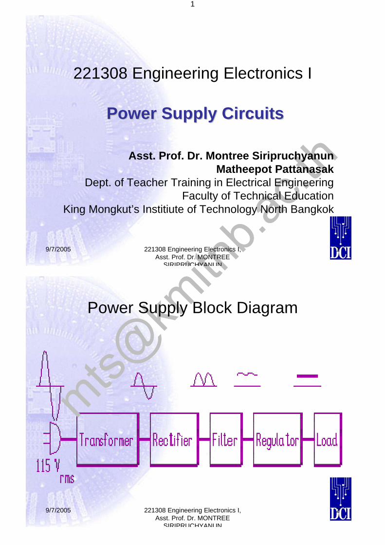
Power Supply Block Diagram
2
9/7/2005 221308 Engineering Electronics I, Asst. Prof. Dr. MONTREE
SIRIPRUCHYANUN
3
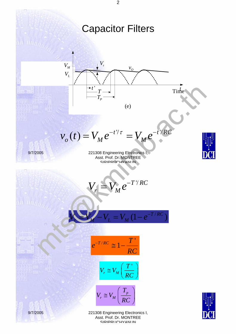
Capacitor Filters
Ov
Time
(e)
rVMV
LV
t't TPT
'/ '/t t RCo M Mv t V e V eτ− −= =
9/7/2005 221308 Engineering Electronics I, Asst. Prof. Dr. MONTREE
SIRIPRUCHYANUN
4
'/T RCr MV V e−=
/(1 )T RCr M L MV V V V e−= − = −
/ '1T RC TeRC
− ≅ −
'r M
TV VRC
⎛ ⎞≅ ⎜ ⎟⎝ ⎠
pr M
TV V
RC⎛ ⎞
≅ ⎜ ⎟⎝ ⎠
3
9/7/2005 221308 Engineering Electronics I, Asst. Prof. Dr. MONTREE
SIRIPRUCHYANUN
5
12 p
fT
=
2M
rVVfRC
=
9/7/2005 221308 Engineering Electronics I, Asst. Prof. Dr. MONTREE
SIRIPRUCHYANUN
6
More Equations . . .
Rearranging the previous equations: VP = Vdc + 1.736 VrThe ripple voltage as a percentage of the dc voltage is:
100% xVVripple
dc
r=
The diode(s) must be rated to withstand the surge current:
W
Psurge R
VI =where RW is the transformer winding’sresistance given by:
FL
FLNLW I
VVR −=
4
9/7/2005 221308 Engineering Electronics I, Asst. Prof. Dr. MONTREE
SIRIPRUCHYANUN
7
Comparison of Different Types of Rectifiers
Half-wave rectifier needs only a single diode but ripple is twice those of the other types.Full-wave rectifier requires a centre-tapped transformer and its output voltage is about half those of the other types.Bridge-type rectifier is best overall even though it requires four diodes because the diode bridge is often available in a single package. However, if a single diode in the bridge is defective, the whole package has to be replaced.
9/7/2005 221308 Engineering Electronics I, Asst. Prof. Dr. MONTREE
SIRIPRUCHYANUN
8
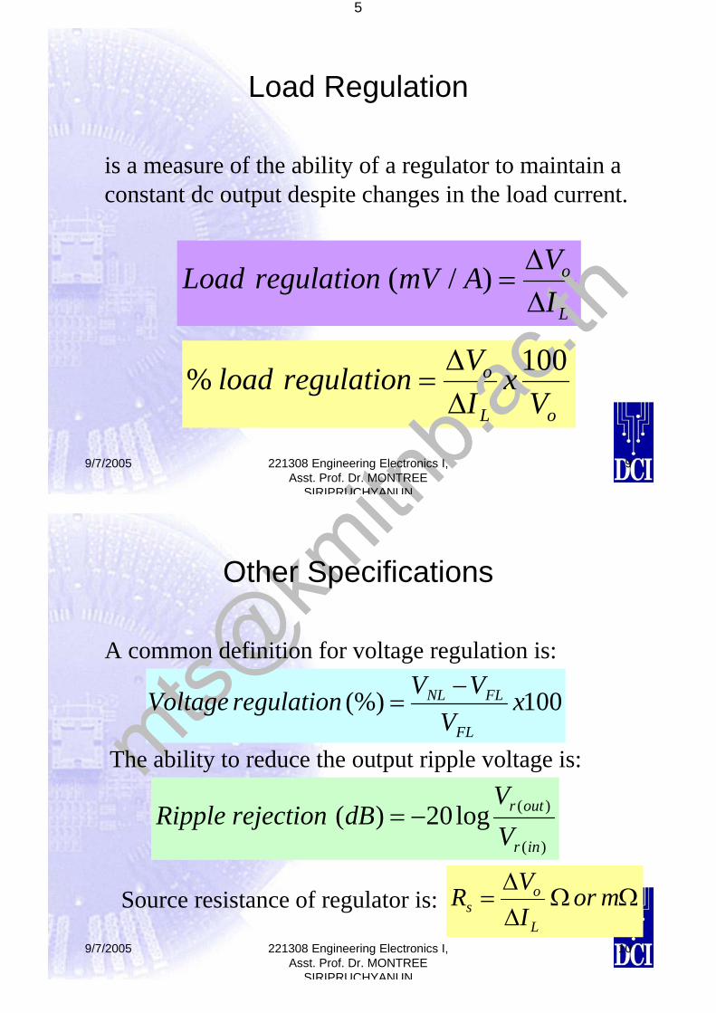
Line Regulation
i
o
VVVmVregulationLine
ΔΔ
=)/(
oi
o
Vx
VVregulationlineΔΔ
=
is a measure of the effectiveness of a voltage regulatorto maintain the output dc voltage constant despitechanges in the supply voltage.
5
9/7/2005 221308 Engineering Electronics I, Asst. Prof. Dr. MONTREE
SIRIPRUCHYANUN
9
Load Regulation
is a measure of the ability of a regulator to maintain aconstant dc output despite changes in the load current.
L
o
IVAmVregulationLoad
ΔΔ
=)/(
oL
o
Vx
IVregulationload 100%
ΔΔ
=
9/7/2005 221308 Engineering Electronics I, Asst. Prof. Dr. MONTREE
SIRIPRUCHYANUN
10
Other Specifications
A common definition for voltage regulation is:
100(%) xV
VVregulationVoltageFL
FLNL −=
The ability to reduce the output ripple voltage is:
)(
)(log20)(inr
outr
VV
dBrejectionRipple −=
Source resistance of regulator is: ΩΩΔΔ
= morIVR
L
os
6
9/7/2005 221308 Engineering Electronics I, Asst. Prof. Dr. MONTREE
SIRIPRUCHYANUN
11
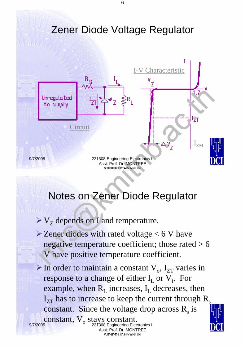
Zener Diode Voltage Regulator
Circuit
I-V Characteristic
IZM
9/7/2005 221308 Engineering Electronics I, Asst. Prof. Dr. MONTREE
SIRIPRUCHYANUN
12
Notes on Zener Diode Regulator
VZ depends on I and temperature.Zener diodes with rated voltage < 6 V have negative temperature coefficient; those rated > 6 V have positive temperature coefficient.In order to maintain a constant Vo, IZT varies in response to a change of either IL or Vi. For example, when RL increases, IL decreases, then IZT has to increase to keep the current through Rsconstant. Since the voltage drop across Rs is constant, Vo stays constant.
7
9/7/2005 221308 Engineering Electronics I, Asst. Prof. Dr. MONTREE
SIRIPRUCHYANUN
13
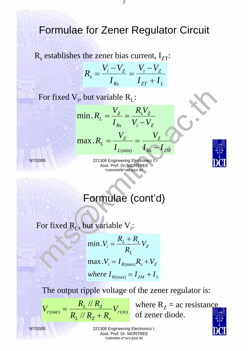
Formulae for Zener Regulator Circuit
Rs establishes the zener bias current, IZT:
LZT
Zi
Rs
Zis II
VVI
VVR+−
=−
=
For fixed Vi, but variable RL:
ZMRs
Z
L
ZL
Zi
Zs
Rs
ZL
IIV
IVR
VVVR
IVR
−==
−==
(min)
.max
.min
9/7/2005 221308 Engineering Electronics I, Asst. Prof. Dr. MONTREE
SIRIPRUCHYANUN
14
Formulae (cont’d)
For fixed RL, but variable Vi:
LZMR
ZsRi
ZL
sLi
IIIwhere
VRIV
VR
RRV
+=
+=
+=
(max)
(max).max
.min
The output ripple voltage of the zener regulator is:
)()( ////
inrsZL
ZLoutr V
RRRRRV+
= where RZ = ac resistanceof zener diode.
8
9/7/2005 221308 Engineering Electronics I, Asst. Prof. Dr. MONTREE
SIRIPRUCHYANUN
15
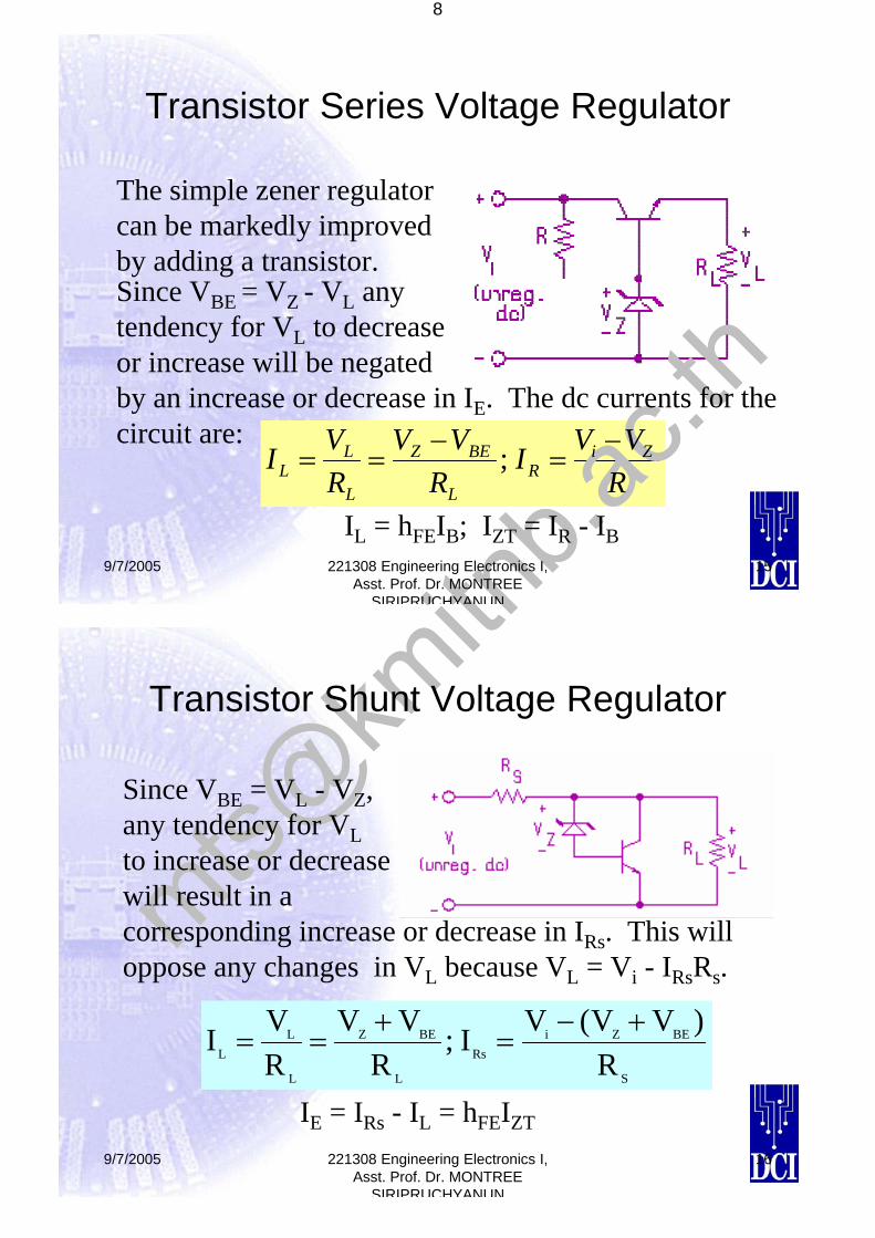
Transistor Series Voltage Regulator
The simple zener regulatorcan be markedly improvedby adding a transistor.Since VBE = VZ - VL anytendency for VL to decrease or increase will be negatedby an increase or decrease in IE. The dc currents for thecircuit are:
RVVI
RVV
RVI Zi
RL
BEZ
L
LL
−=
−== ;
IL = hFEIB; IZT = IR - IB
9/7/2005 221308 Engineering Electronics I, Asst. Prof. Dr. MONTREE
SIRIPRUCHYANUN
16
Transistor Shunt Voltage Regulator
Since VBE = VL - VZ,any tendency for VLto increase or decreasewill result in a corresponding increase or decrease in IRs. This willoppose any changes in VL because VL = Vi - IRsRs.
S
BEZiRs
L
BEZ
L
LL R
)VV(VI;R
VVRVI +−
=+
==
IE = IRs - IL = hFEIZT
9
9/7/2005 221308 Engineering Electronics I, Asst. Prof. Dr. MONTREE
SIRIPRUCHYANUN
17
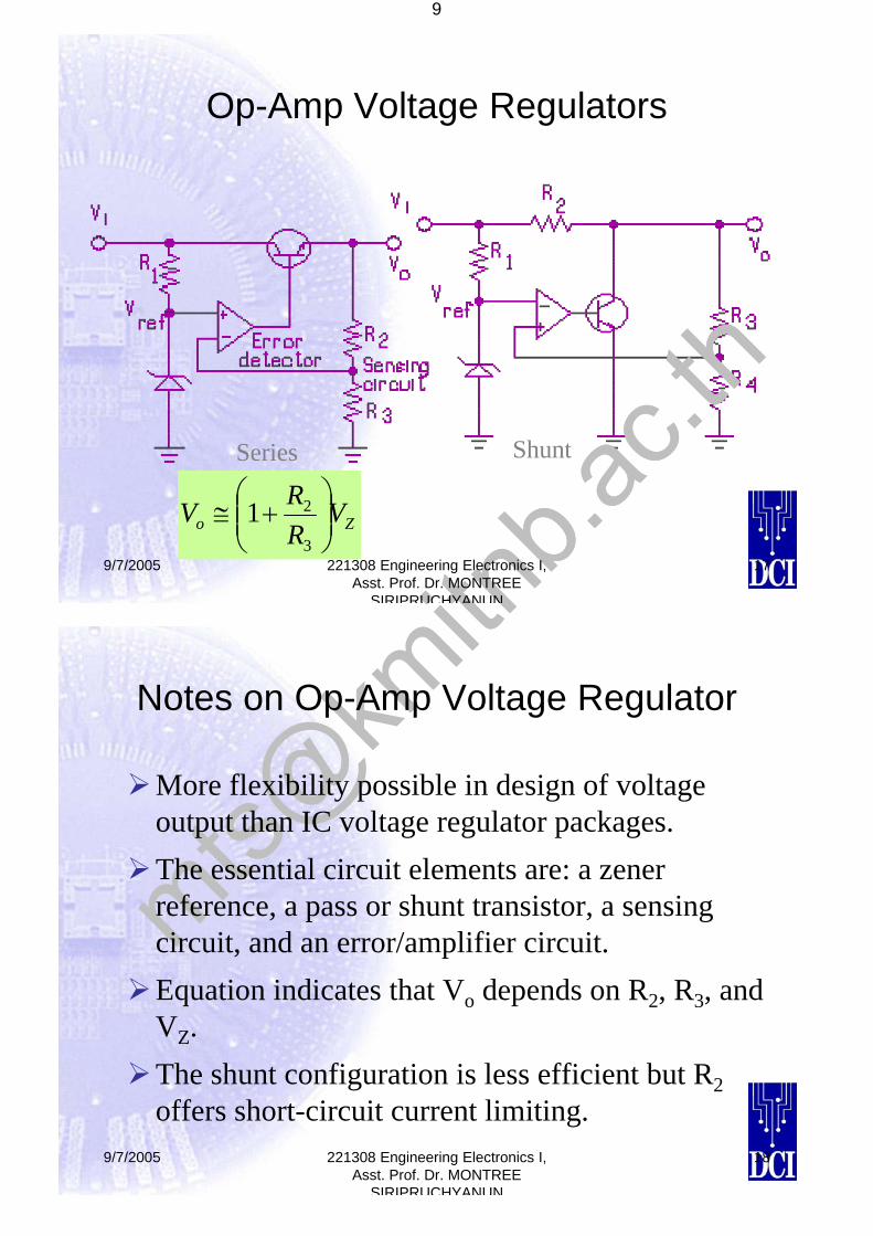
Op-Amp Voltage Regulators
Zo VRRV ⎟⎟
⎠
⎞⎜⎜⎝
⎛+≅
3
21
Series Shunt
9/7/2005 221308 Engineering Electronics I, Asst. Prof. Dr. MONTREE
SIRIPRUCHYANUN
18
Notes on Op-Amp Voltage Regulator
More flexibility possible in design of voltage output than IC voltage regulator packages.The essential circuit elements are: a zenerreference, a pass or shunt transistor, a sensing circuit, and an error/amplifier circuit.Equation indicates that Vo depends on R2, R3, and VZ.The shunt configuration is less efficient but R2offers short-circuit current limiting.
10
9/7/2005 221308 Engineering Electronics I, Asst. Prof. Dr. MONTREE
SIRIPRUCHYANUN
19
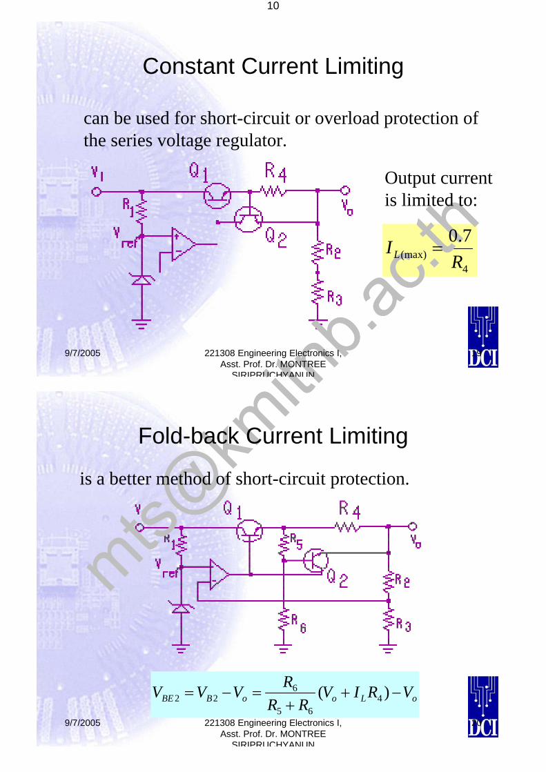
Constant Current Limiting
can be used for short-circuit or overload protection ofthe series voltage regulator.
4(max)
7.0R
IL =
Output currentis limited to:
9/7/2005 221308 Engineering Electronics I, Asst. Prof. Dr. MONTREE
SIRIPRUCHYANUN
20
Fold-back Current Limiting
is a better method of short-circuit protection.
oLooBBE VRIVRR
RVVV −++
=−= )( 465
622
11
9/7/2005 221308 Engineering Electronics I, Asst. Prof. Dr. MONTREE
SIRIPRUCHYANUN
21
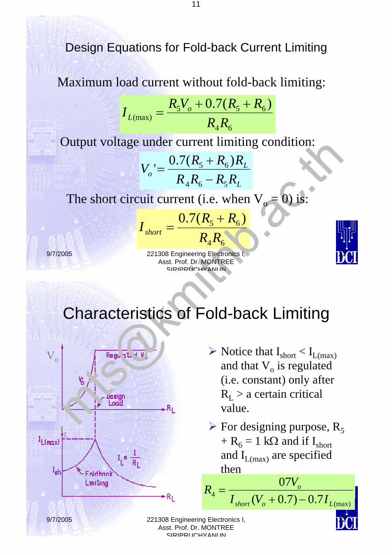
Design Equations for Fold-back Current Limiting
Maximum load current without fold-back limiting:
64
655(max)
)(7.0RR
RRVRI oL
++=
Output voltage under current limiting condition:
L
Lo RRRR
RRRV564
65 )(7.0'−+
=
The short circuit current (i.e. when Vo = 0) is:
64
65 )(7.0RR
RRIshort+
=
9/7/2005 221308 Engineering Electronics I, Asst. Prof. Dr. MONTREE
SIRIPRUCHYANUN
22
Characteristics of Fold-back Limiting
Notice that Ishort < IL(max)and that Vo is regulated (i.e. constant) only after RL > a certain critical value.For designing purpose, R5+ R6 = 1 kΩ and if Ishortand IL(max) are specified then
(max)4 7.0)7.0(
07
Loshort
o
IVIVR−+
=
Vo
IL
12
9/7/2005 221308 Engineering Electronics I, Asst. Prof. Dr. MONTREE
SIRIPRUCHYANUN
23
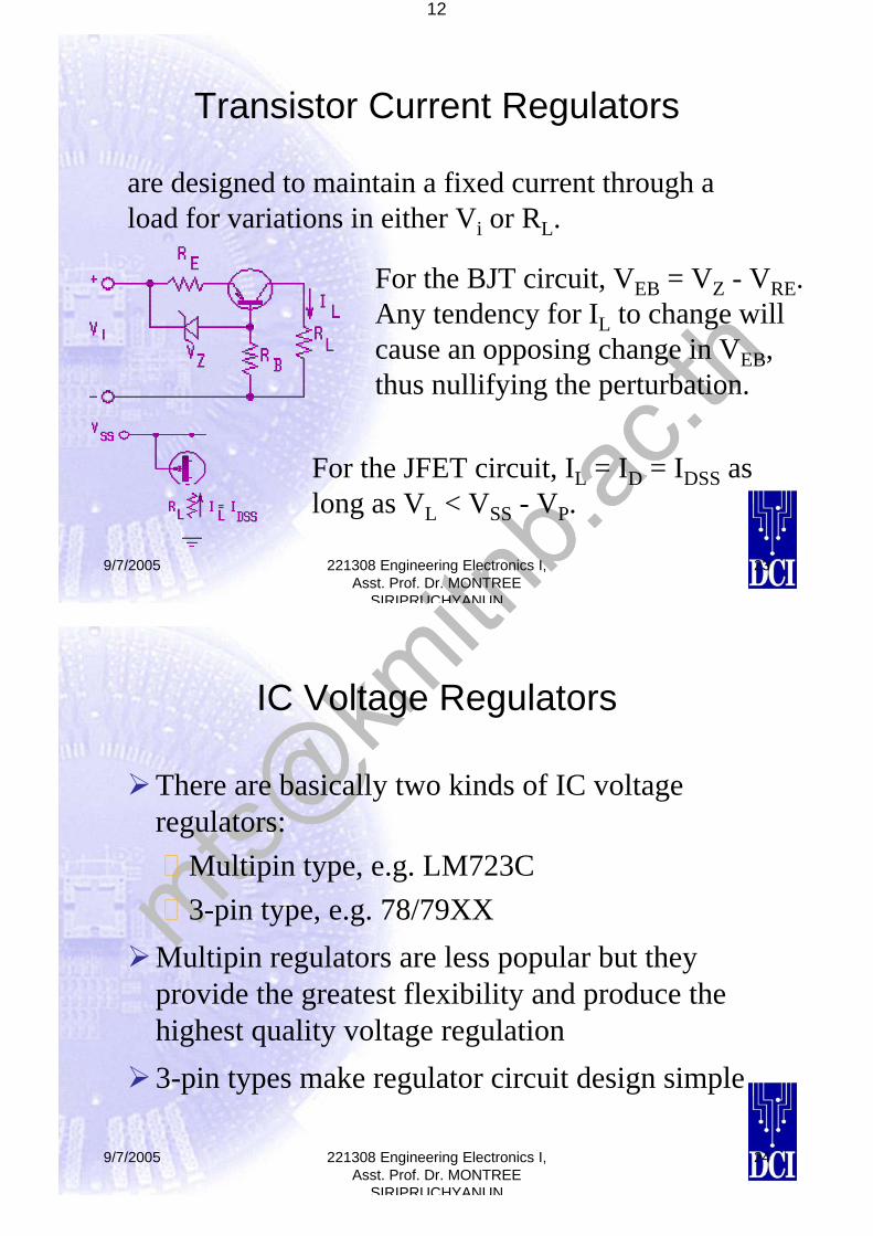
Transistor Current Regulators
are designed to maintain a fixed current through aload for variations in either Vi or RL.
For the BJT circuit, VEB = VZ - VRE.Any tendency for IL to change willcause an opposing change in VEB,thus nullifying the perturbation.
For the JFET circuit, IL = ID = IDSS aslong as VL < VSS - VP.
9/7/2005 221308 Engineering Electronics I, Asst. Prof. Dr. MONTREE
SIRIPRUCHYANUN
24
IC Voltage Regulators
There are basically two kinds of IC voltage regulators:
Multipin type, e.g. LM723C3-pin type, e.g. 78/79XX
Multipin regulators are less popular but they provide the greatest flexibility and produce the highest quality voltage regulation3-pin types make regulator circuit design simple
13
9/7/2005 221308 Engineering Electronics I, Asst. Prof. Dr. MONTREE
SIRIPRUCHYANUN
25
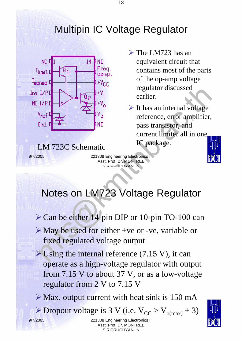
Multipin IC Voltage Regulator
LM 723C Schematic
The LM723 has an equivalent circuit that contains most of the parts of the op-amp voltage regulator discussed earlier.It has an internal voltage reference, error amplifier, pass transistor, and current limiter all in one IC package.
9/7/2005 221308 Engineering Electronics I, Asst. Prof. Dr. MONTREE
SIRIPRUCHYANUN
26
Notes on LM723 Voltage Regulator
Can be either 14-pin DIP or 10-pin TO-100 canMay be used for either +ve or -ve, variable or fixed regulated voltage outputUsing the internal reference (7.15 V), it can operate as a high-voltage regulator with output from 7.15 V to about 37 V, or as a low-voltage regulator from 2 V to 7.15 VMax. output current with heat sink is 150 mADropout voltage is 3 V (i.e. VCC > Vo(max) + 3)
14
9/7/2005 221308 Engineering Electronics I, Asst. Prof. Dr. MONTREE
SIRIPRUCHYANUN
27
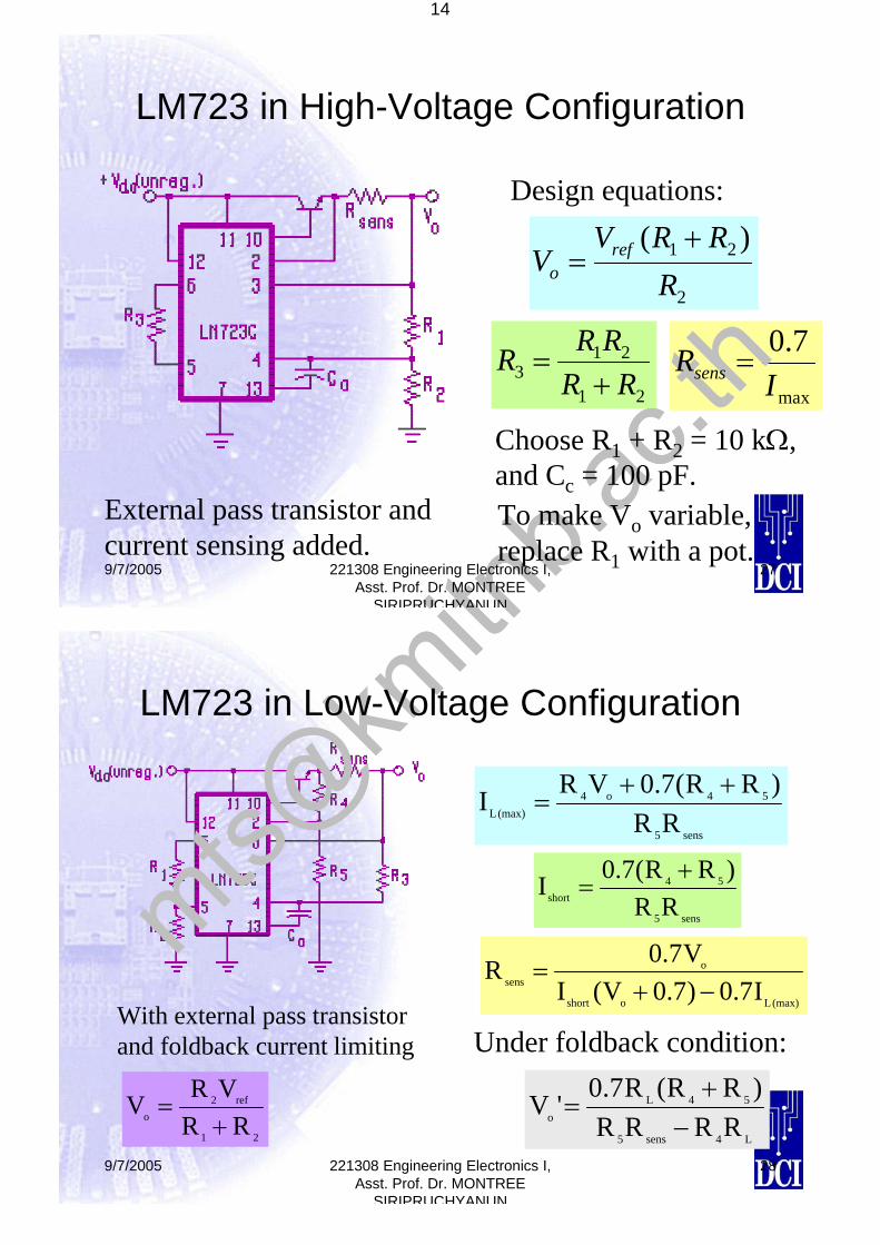
LM723 in High-Voltage Configuration
External pass transistor andcurrent sensing added.
Design equations:
2
21 )(R
RRVV ref
o
+=
21
213 RR
RRR+
=max
7.0I
Rsens =
Choose R1 + R2 = 10 kΩ,and Cc = 100 pF.To make Vo variable,replace R1 with a pot.
9/7/2005 221308 Engineering Electronics I, Asst. Prof. Dr. MONTREE
SIRIPRUCHYANUN
28
LM723 in Low-Voltage Configuration
With external pass transistorand foldback current limiting
sens5
54o4(max)L RR
)RR(7.0VRI ++=
sens5
54short RR
)RR(7.0I +=
(max)Loshort
osens I7.0)7.0V(I
V7.0R−+
=
L4sens5
54Lo RRRR
)RR(R7.0'V−+
=
Under foldback condition:
21
ref2o RR
VRV+
=
15
9/7/2005 221308 Engineering Electronics I, Asst. Prof. Dr. MONTREE
SIRIPRUCHYANUN
29
Three-Terminal Fixed Voltage RegulatorsLess flexible, but simple to useCome in standard TO-3 (20 W) or TO-220 (15 W) transistor packages78/79XX series regulators are commonly available with 5, 6, 8, 12, 15, 18, or 24 V outputMax. output current with heat sink is 1 ABuilt-in thermal shutdown protection3-V dropout voltage; max. input of 37 VRegulators with lower dropout, higher in/output, and better regulation are available.
9/7/2005 221308 Engineering Electronics I, Asst. Prof. Dr. MONTREE
SIRIPRUCHYANUN
30
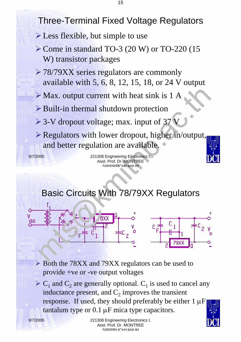
Basic Circuits With 78/79XX Regulators
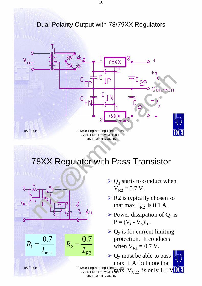
Both the 78XX and 79XX regulators can be used to provide +ve or -ve output voltagesC1 and C2 are generally optional. C1 is used to cancel any inductance present, and C2 improves the transient response. If used, they should preferably be either 1 μF tantalum type or 0.1 μF mica type capacitors.
16
9/7/2005 221308 Engineering Electronics I, Asst. Prof. Dr. MONTREE
SIRIPRUCHYANUN
31
Dual-Polarity Output with 78/79XX Regulators
9/7/2005 221308 Engineering Electronics I, Asst. Prof. Dr. MONTREE
SIRIPRUCHYANUN
32
78XX Regulator with Pass Transistor
Q1 starts to conduct when VR2 = 0.7 V.R2 is typically chosen so that max. IR2 is 0.1 A.Power dissipation of Q1 is P = (Vi - Vo)IL.Q2 is for current limiting protection. It conducts when VR1 = 0.7 V.Q2 must be able to pass max. 1 A; but note that max. VCE2 is only 1.4 V.
max1
7.0I
R =2
27.0
RIR =
17
9/7/2005 221308 Engineering Electronics I, Asst. Prof. Dr. MONTREE
SIRIPRUCHYANUN
33
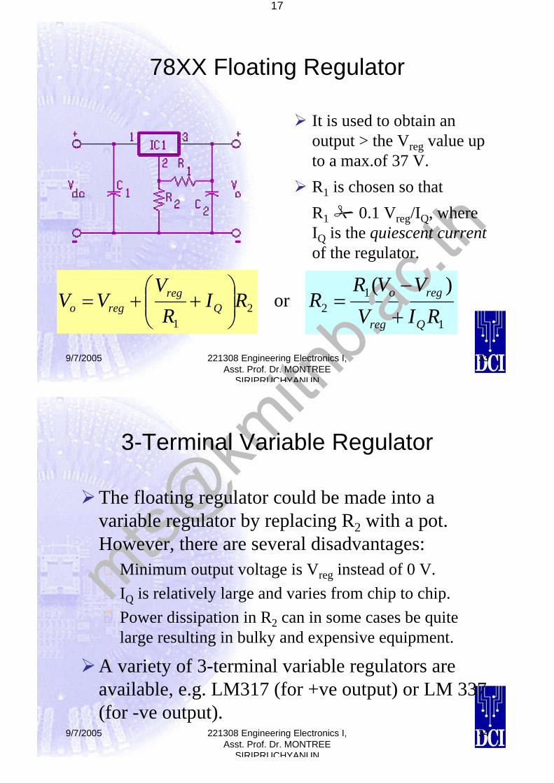
78XX Floating Regulator
It is used to obtain an output > the Vreg value up to a max.of 37 V.R1 is chosen so thatR1 0.1 Vreg/IQ, where IQ is the quiescent currentof the regulator.
21
RIR
VVV Q
regrego ⎟⎟
⎠
⎞⎜⎜⎝
⎛++=
1
12
)(RIV
VVRR
Qreg
rego
+
−=or
9/7/2005 221308 Engineering Electronics I, Asst. Prof. Dr. MONTREE
SIRIPRUCHYANUN
34
3-Terminal Variable Regulator
The floating regulator could be made into a variable regulator by replacing R2 with a pot. However, there are several disadvantages:
Minimum output voltage is Vreg instead of 0 V.IQ is relatively large and varies from chip to chip.Power dissipation in R2 can in some cases be quite large resulting in bulky and expensive equipment.
A variety of 3-terminal variable regulators are available, e.g. LM317 (for +ve output) or LM 337 (for -ve output).
18
9/7/2005 221308 Engineering Electronics I, Asst. Prof. Dr. MONTREE
SIRIPRUCHYANUN
35
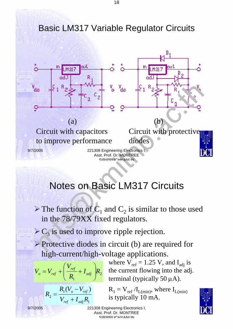
Basic LM317 Variable Regulator Circuits
Circuit with capacitorsto improve performance
Circuit with protectivediodes
(a) (b)
9/7/2005 221308 Engineering Electronics I, Asst. Prof. Dr. MONTREE
SIRIPRUCHYANUN
36
Notes on Basic LM317 Circuits
The function of C1 and C2 is similar to those used in the 78/79XX fixed regulators.C3 is used to improve ripple rejection.Protective diodes in circuit (b) are required for high-current/high-voltage applications.
21
RIR
VVV adj
refrefo ⎟⎟
⎠
⎞⎜⎜⎝
⎛++=
where Vref = 1.25 V, and Iadj isthe current flowing into the adj.terminal (typically 50 μA).
1
12
)(RIV
VVRR
adjref
refo
+
−=
R1 = Vref /IL(min), where IL(min)is typically 10 mA.
19
9/7/2005 221308 Engineering Electronics I, Asst. Prof. Dr. MONTREE
SIRIPRUCHYANUN
37
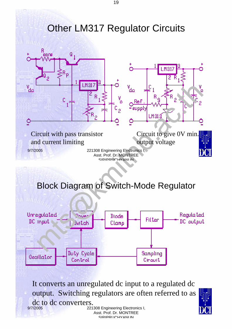
Other LM317 Regulator Circuits
Circuit with pass transistorand current limiting
Circuit to give 0V min.output voltage
9/7/2005 221308 Engineering Electronics I, Asst. Prof. Dr. MONTREE
SIRIPRUCHYANUN
38
Block Diagram of Switch-Mode Regulator
It converts an unregulated dc input to a regulated dcoutput. Switching regulators are often referred to asdc to dc converters.
20
9/7/2005 221308 Engineering Electronics I, Asst. Prof. Dr. MONTREE
SIRIPRUCHYANUN
39
Comparing Switch-Mode to Linear Regulators
Advantages:70-90% efficiency (about double that of linear ones)can make output voltage > input voltage, if desiredcan invert the input voltageconsiderable weight and size reductions, especially at high output power
Disadvantages:More complex circuitry Potential EMI problems unless good shielding, low-loss ferrite cores and chokes are used
9/7/2005 221308 Engineering Electronics I, Asst. Prof. Dr. MONTREE
SIRIPRUCHYANUN
40
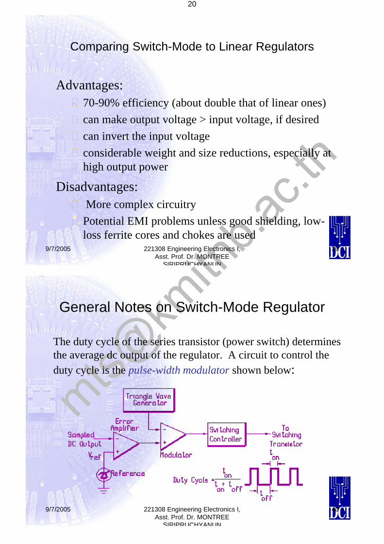
General Notes on Switch-Mode Regulator
The duty cycle of the series transistor (power switch) determinesthe average dc output of the regulator. A circuit to control theduty cycle is the pulse-width modulator shown below:
21
9/7/2005 221308 Engineering Electronics I, Asst. Prof. Dr. MONTREE
SIRIPRUCHYANUN
41
General Notes cont’d . . .
The error amplifier compares a sample of the regulator Vo to an internal Vref. The difference or error voltage is amplified and applied to a modulator where it is compared to a triangle waveform. The result is an output pulse whose width is proportional to the error voltage.Darlington transistors and TMOS FETs with fT of at least 4 MHz are often used. TMOS FETs are more efficient.A fast-recovery rectifier, or a Schottky barrier diode (sometimes referred to as a catch diode) is used to direct current into the inductor.For proper switch-mode operation, current must always be present in the inductor.
9/7/2005 221308 Engineering Electronics I, Asst. Prof. Dr. MONTREE
SIRIPRUCHYANUN
42
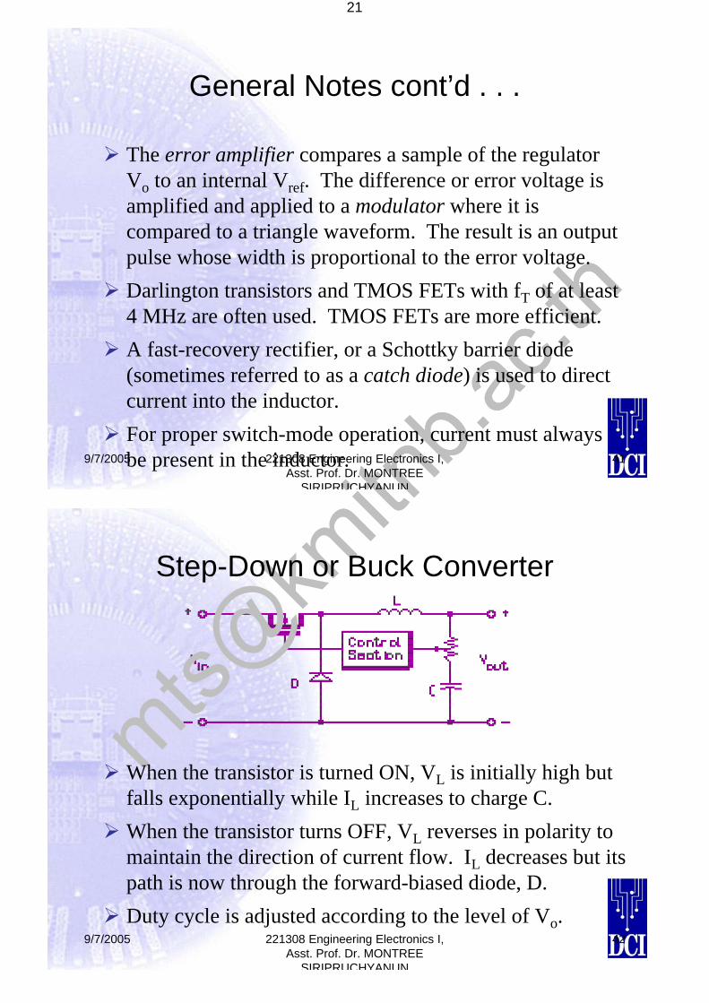
Step-Down or Buck Converter
When the transistor is turned ON, VL is initially high but falls exponentially while IL increases to charge C.When the transistor turns OFF, VL reverses in polarity to maintain the direction of current flow. IL decreases but its path is now through the forward-biased diode, D.Duty cycle is adjusted according to the level of Vo.
22
9/7/2005 221308 Engineering Electronics I, Asst. Prof. Dr. MONTREE
SIRIPRUCHYANUN
43
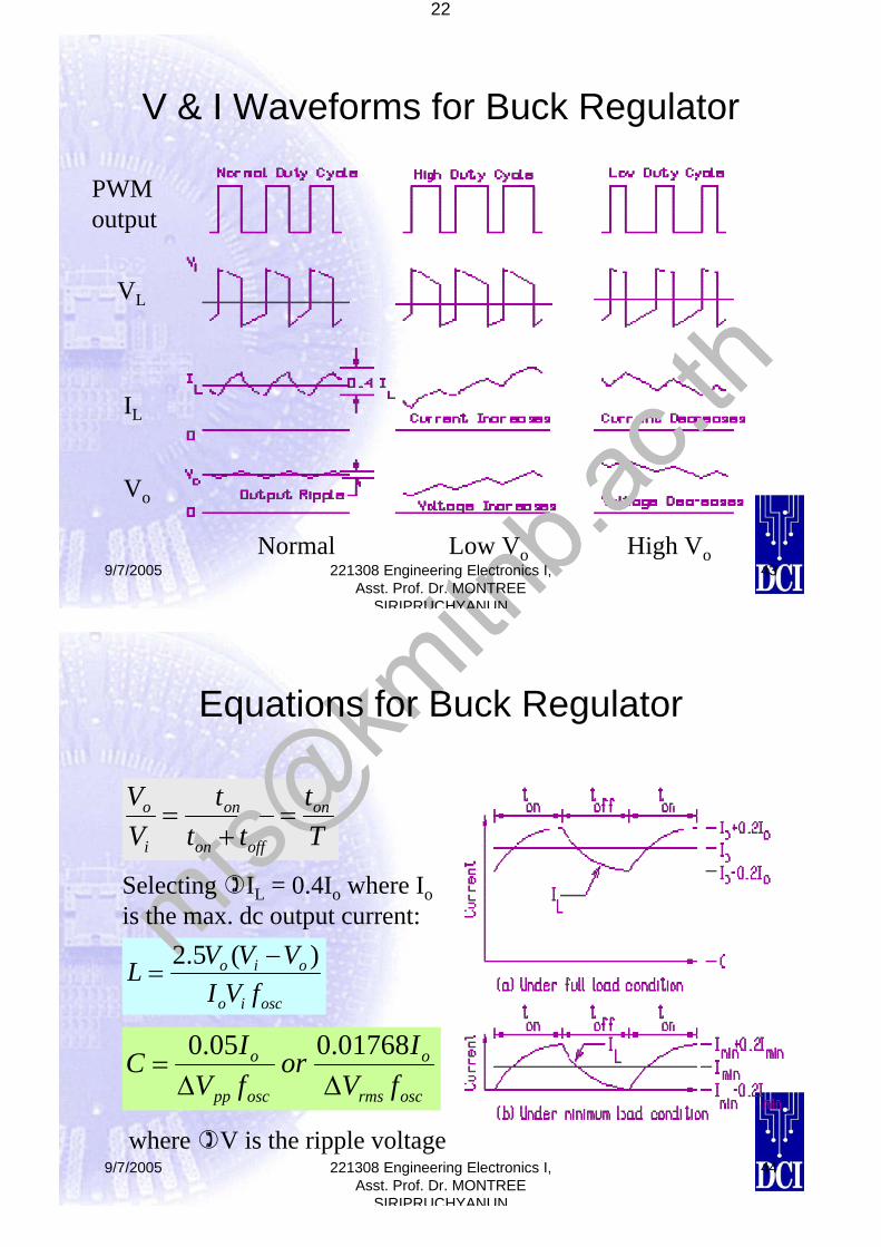
V & I Waveforms for Buck Regulator
PWMoutput
VL
IL
Vo
Normal Low Vo High Vo
9/7/2005 221308 Engineering Electronics I, Asst. Prof. Dr. MONTREE
SIRIPRUCHYANUN
44
Equations for Buck Regulator
Tt
ttt
VV on
offon
on
i
o =+
=
Selecting IL = 0.4Io where Iois the max. dc output current:
oscio
oio
fVIVVVL )(5.2 −
=
oscrms
o
oscpp
o
fVIor
fVIC
ΔΔ=
01768.005.0
where V is the ripple voltage
23
9/7/2005 221308 Engineering Electronics I, Asst. Prof. Dr. MONTREE
SIRIPRUCHYANUN
45
Notes on Operation of Buck Regulator
When IL = 0.4Io was selected, the average minimum current, Imin, that must be maintained in L for proper regulator operation is 0.2Io.If IL is chosen to be 4% instead of 40% of Io, the 2.5 factor in the equation for L becomes 25 and Imin becomes 0.02Io.L and C are both proportional to 1/fosc; hence, the higher fosc is the smaller L and C become. But for predictable operation and less audible noise, fosc is usually between 50kHz to 100 kHz.
9/7/2005 221308 Engineering Electronics I, Asst. Prof. Dr. MONTREE
SIRIPRUCHYANUN
46
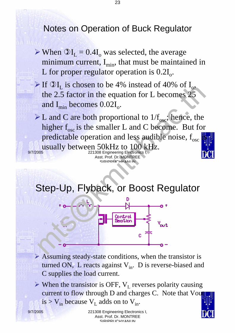
Step-Up, Flyback, or Boost Regulator
Assuming steady-state conditions, when the transistor is turned ON, L reacts against Vin. D is reverse-biased and C supplies the load current.When the transistor is OFF, VL reverses polarity causing current to flow through D and charges C. Note that Voutis > Vin because VL adds on to Vin.
24
9/7/2005 221308 Engineering Electronics I, Asst. Prof. Dr. MONTREE
SIRIPRUCHYANUN
47
Equations for Boost Regulator
Tt
VVV on
o
io =−
oscoo
ioi
fVIVVVL 2
2 )(5.2 −=
Assuming IL = 0.4Io:
rmsoosc
oio
ppoosc
oio
VVfIVVor
VVfIVVC
Δ−
Δ−
=)(3536.0)(
9/7/2005 221308 Engineering Electronics I, Asst. Prof. Dr. MONTREE
SIRIPRUCHYANUN
48
Voltage-Inverting or Buck-Boost Regulator
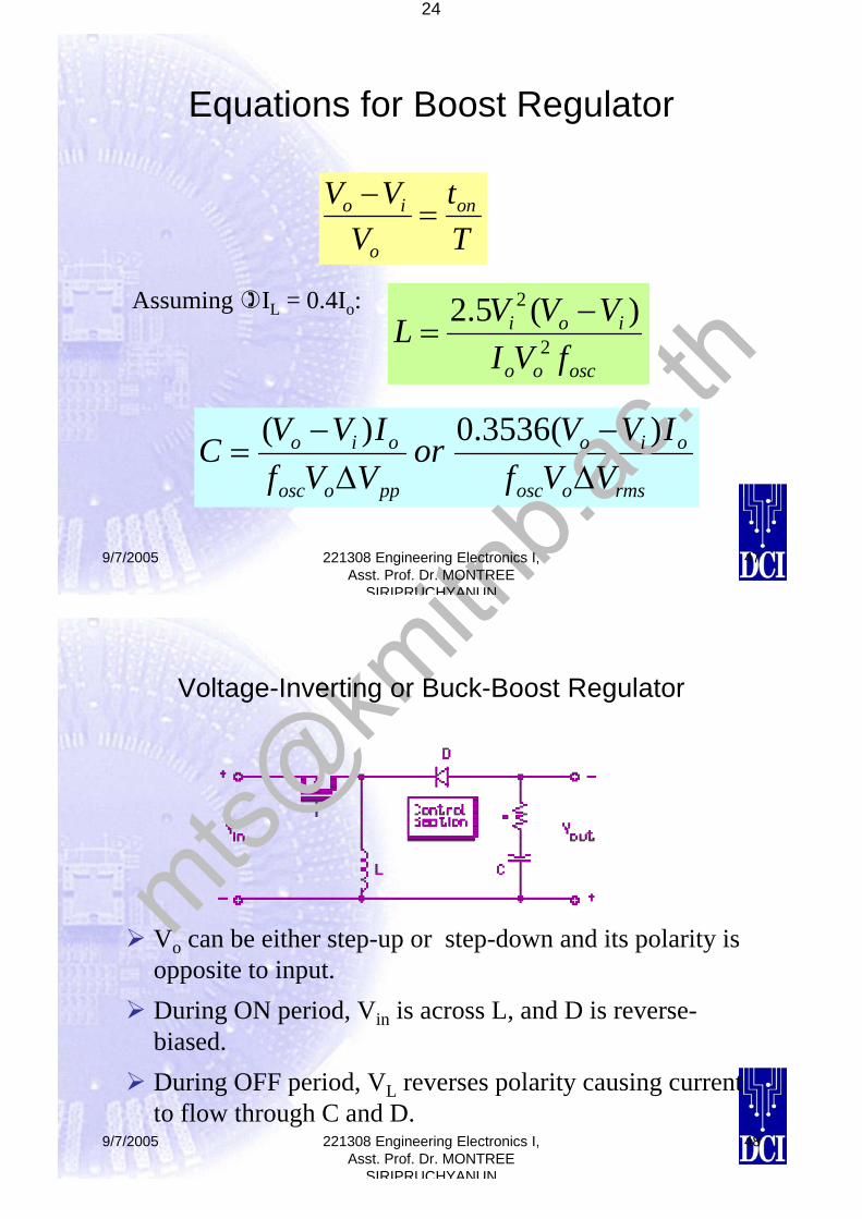
Vo can be either step-up or step-down and its polarity is opposite to input.During ON period, Vin is across L, and D is reverse-biased.During OFF period, VL reverses polarity causing current to flow through C and D.
25
9/7/2005 221308 Engineering Electronics I, Asst. Prof. Dr. MONTREE
SIRIPRUCHYANUN
49
Equations for Buck-Boost Regulator
Tt
VVV on
oi
o =+
For IL = 0.4Io:
oscioo
oi
fVVIVVL
)(5.2+
=
oscoirms
oo
oscoipp
oo
fVVVVIor
fVVVVIC
)(3536.0
)( +Δ+Δ=
9/7/2005 221308 Engineering Electronics I, Asst. Prof. Dr. MONTREE
SIRIPRUCHYANUN
50
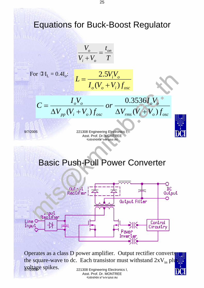
Basic Push-Pull Power Converter
Operates as a class D power amplifier. Output rectifier converts the square-wave to dc. Each transistor must withstand 2xVin plusvoltage spikes.
26
9/7/2005 221308 Engineering Electronics I, Asst. Prof. Dr. MONTREE
SIRIPRUCHYANUN
51
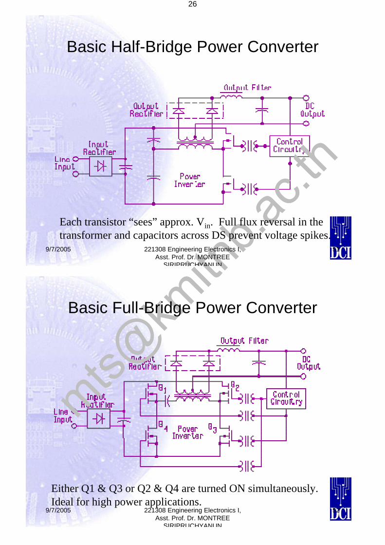
Basic Half-Bridge Power Converter
Each transistor “sees” approx. Vin. Full flux reversal in the transformer and capacitors across DS prevent voltage spikes.
9/7/2005 221308 Engineering Electronics I, Asst. Prof. Dr. MONTREE
SIRIPRUCHYANUN
52
Basic Full-Bridge Power Converter
Either Q1 & Q3 or Q2 & Q4 are turned ON simultaneously.Ideal for high power applications.
27
9/7/2005 221308 Engineering Electronics I, Asst. Prof. Dr. MONTREE
SIRIPRUCHYANUN
53
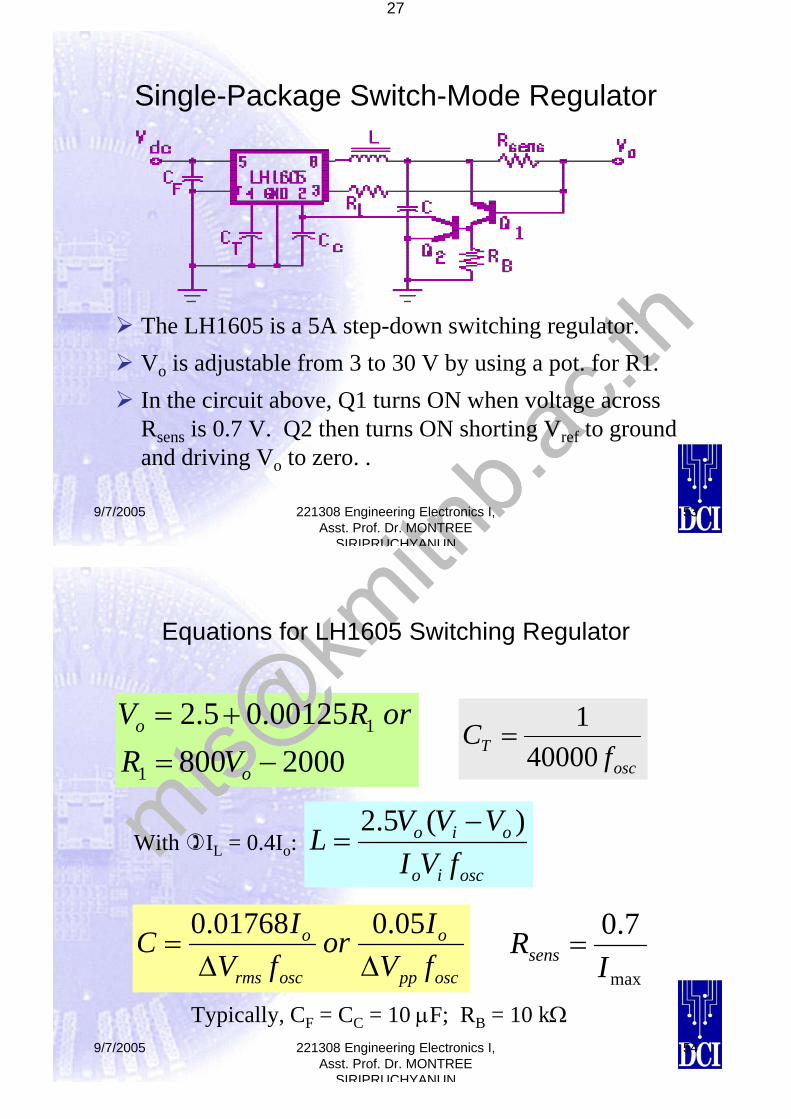
Single-Package Switch-Mode Regulator
The LH1605 is a 5A step-down switching regulator.Vo is adjustable from 3 to 30 V by using a pot. for R1.In the circuit above, Q1 turns ON when voltage across Rsens is 0.7 V. Q2 then turns ON shorting Vref to ground and driving Vo to zero. .
9/7/2005 221308 Engineering Electronics I, Asst. Prof. Dr. MONTREE
SIRIPRUCHYANUN
54
Equations for LH1605 Switching Regulator
200080000125.05.2
1
1
−=+=
o
o
VRorRV
oscT f
C40000
1=
oscio
oio
fVIVVVL )(5.2 −
=With IL = 0.4Io:
oscpp
o
oscrms
o
fVIor
fVIC
ΔΔ=
05.001768.0
max
7.0I
Rsens =
Typically, CF = CC = 10 μF; RB = 10 kΩ