Embed Size (px)
Citation preview
MicroBlaze Tutorial
Introduction
This tutorial guides you through the process of using Xilinx Embedded Development Kit (EDK) software tools, in which this tutorial will use the Xilinx Platform Studio (XPS) tool to create a simple processor system. ISE Version: 9.2i or 10.1i
Objectives
This processor project should perform two simple jobs.First, it toggles the LED on the board off and on. Secondly, it continuously prints "Microblaze" to the screen.
Process
1. Step through the project design steps. 2. Verify outputs on HyperTerminal.
Implementation 1. Open the Xilinx Platform Studio by selecting it from the start menu.
Figure 1 XPS Project Selection

2. The Xilinx Platform Studio, or XPS, Base System Builder will launch. For the purposes of this tutorial, it is important to use the Wizard. Select the top option.
Figure 2 Project Directory Selection
3. Choose a directory for the sample project. Avoid directory names with spaces in them.

Figure 3 BSB Screen
4. Choose to create a new design. The BSB (Base System Builder) allows the user to be able to open a new design or to import the BSB settings from a previous project. Click Next and it will show the Base System Builder window.
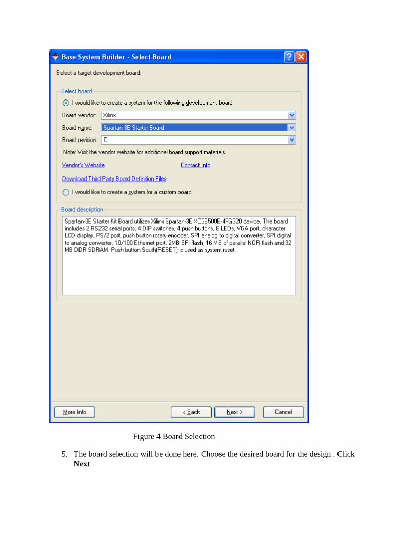
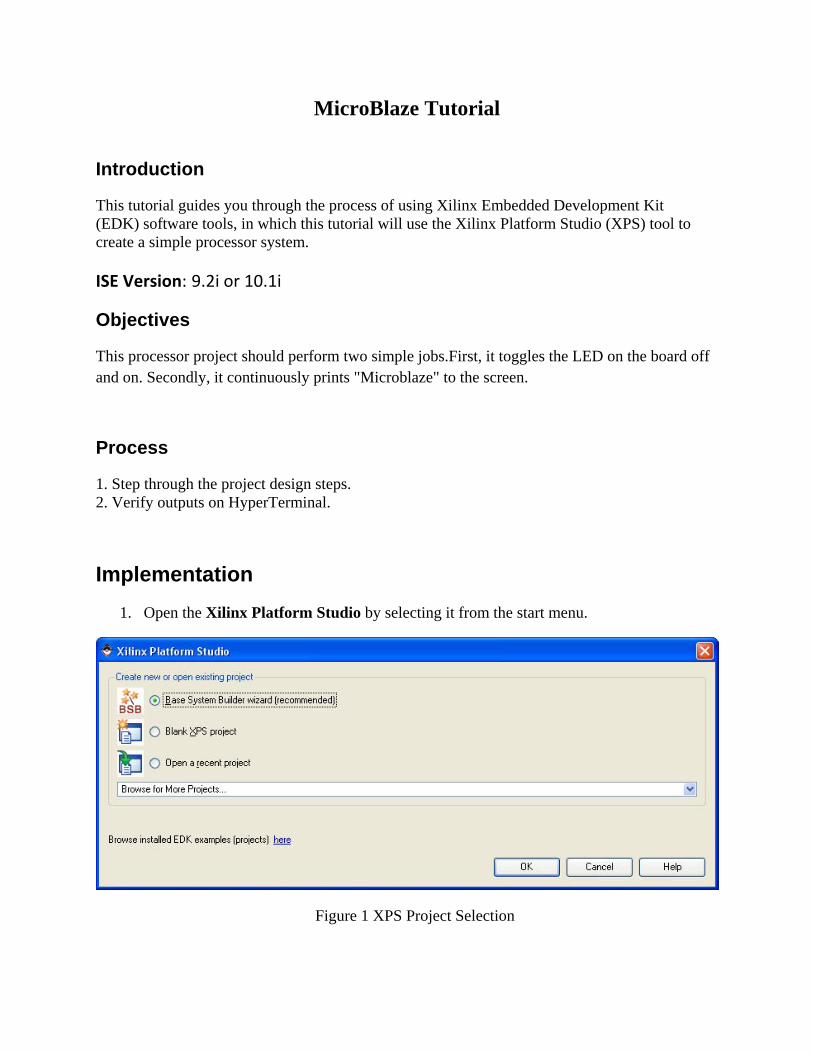
Figure 4 Board Selection
5. The board selection will be done here. Choose the desired board for the design . Click Next

Figure 5 Processor Type
6. Select Next, saving the Microblaze as the processor to use in this design. (The EDK software allows the user to create a project for one of two types of processors. The
first (and the one selected) is a virtual processor called the Microblaze. This processor is created within the fabric of the FPGA. The second type is the PowerPC. This is the IBM PPC405 which is actually embedded into the fabric of the FPGA.)
Figure 6 Basic Selections
7. Select Next, saving the default settings. (This is a menu specifically designed to configure the Microblaze. If there were a desire to change the clock frequencies then
they could be done here. By clicking on the “More Info” button, more information on the changeable values can be obtained.)

Figure 7 Screen 1 of 3 for Interfaces
8. This is the first of three screens for choosing input and output interfaces. As shown in the screen above, select the OPB UARTLITE and LED. Deselect all other options, and then click Next. This project will only have four items associated with the outer peripheral Bus or OPB. The four items used will be the UART, LED, PUSHBUTTON and the BRAM.
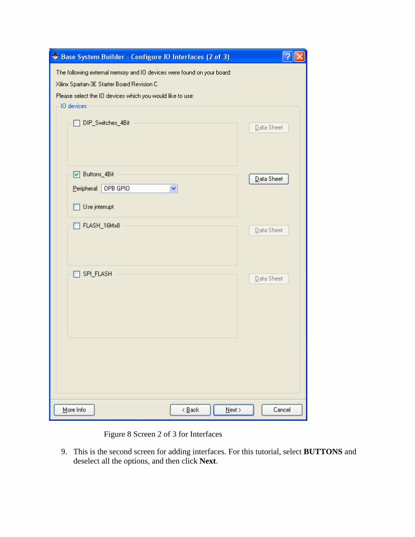
Figure 8 Screen 2 of 3 for Interfaces
9. This is the second screen for adding interfaces. For this tutorial, select BUTTONS and deselect all the options, and then click Next.
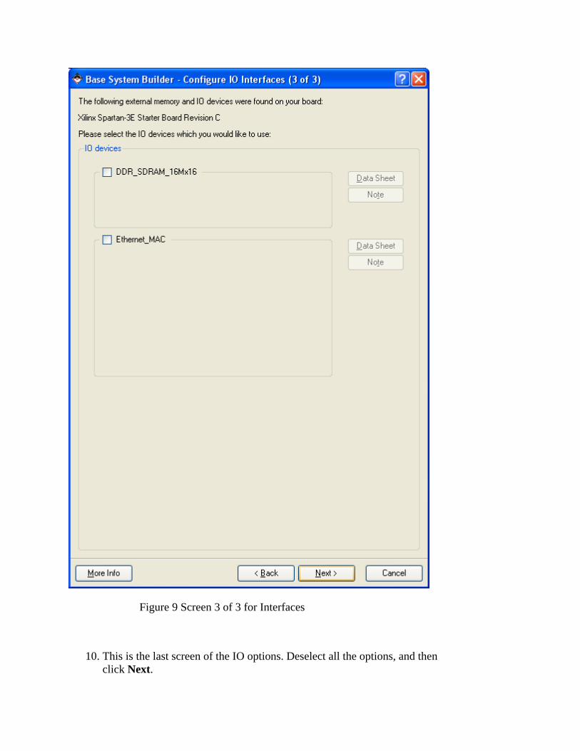
Figure 9 Screen 3 of 3 for Interfaces
10. This is the last screen of the IO options. Deselect all the options, and then click Next.

Figure 10 Internal Peripherals
11. Choose 8KB - 64KB of BRAM as per project requirement, and then select Next.
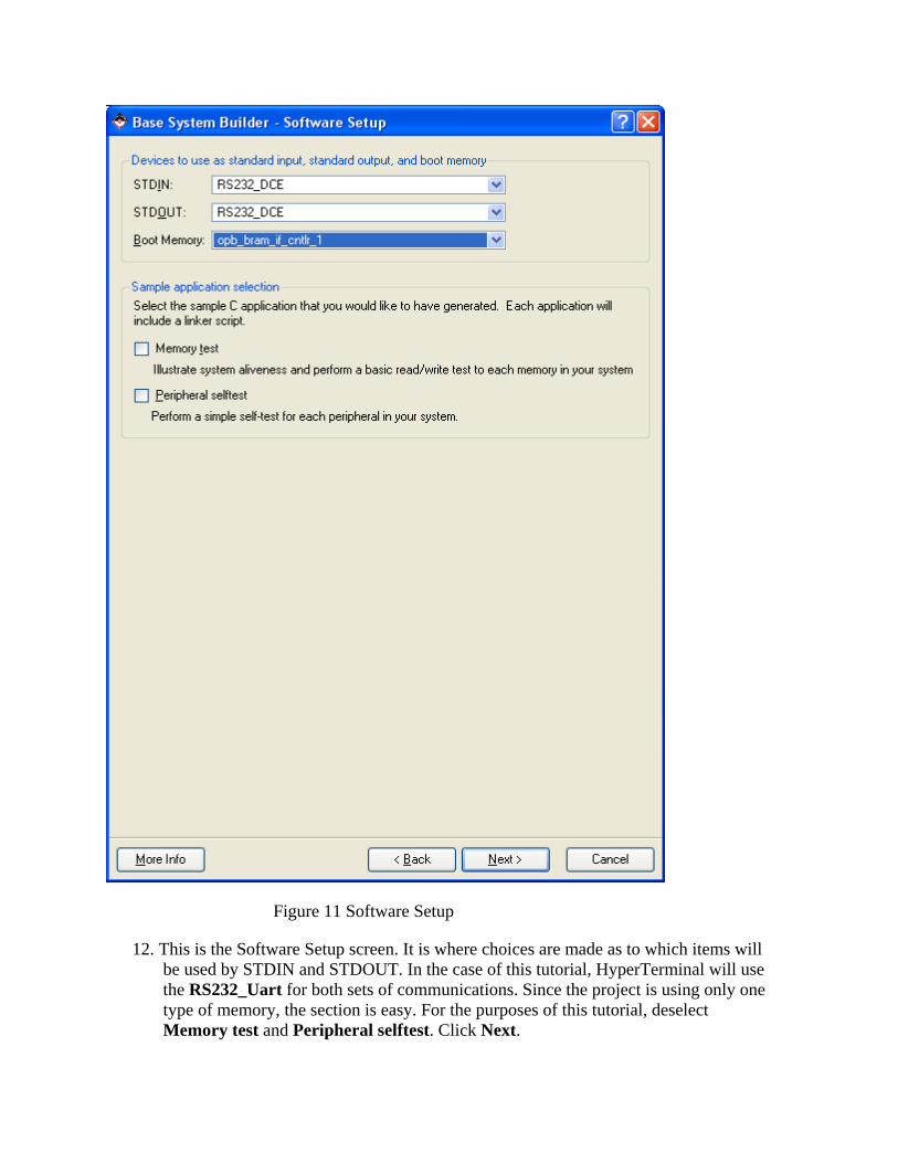
Figure 11 Software Setup
12. This is the Software Setup screen. It is where choices are made as to which items will be used by STDIN and STDOUT. In the case of this tutorial, HyperTerminal will use the RS232_Uart for both sets of communications. Since the project is using only one type of memory, the section is easy. For the purposes of this tutorial, deselect Memory test and Peripheral selftest. Click Next.
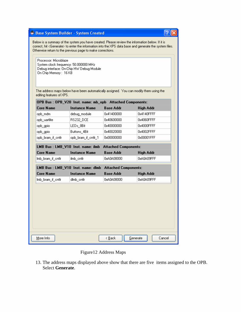
Figure12 Address Maps
13. The address maps displayed above show that there are five items assigned to the OPB. Select Generate.
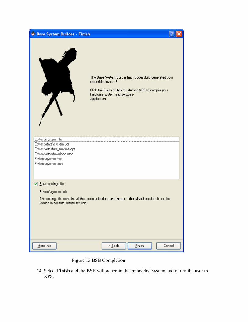
Figure 13 BSB Completion
14. Select Finish and the BSB will generate the embedded system and return the user to XPS.

Figure 14 Platform Selection
15. Select Platform Studio for system assembly view.
Figure 15 OPB Connections
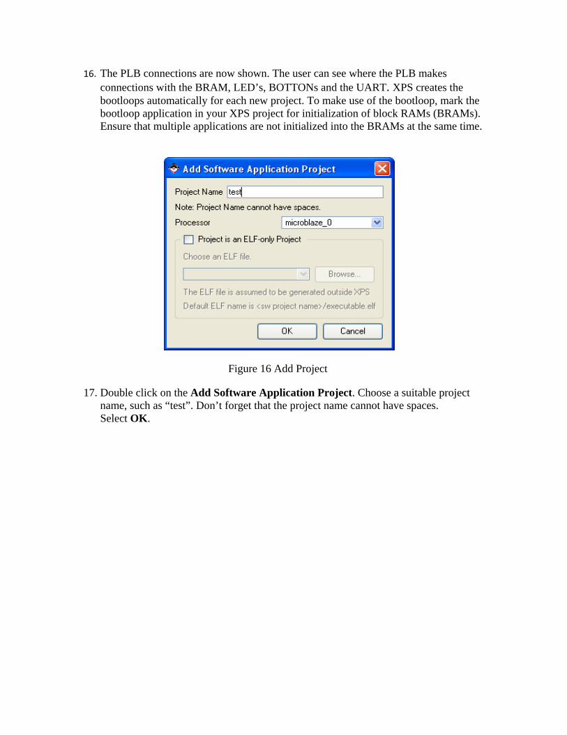
16. The PLB connections are now shown. The user can see where the PLB makes connections with the BRAM, LED’s, BOTTONs and the UART. XPS creates the bootloops automatically for each new project. To make use of the bootloop, mark the bootloop application in your XPS project for initialization of block RAMs (BRAMs). Ensure that multiple applications are not initialized into the BRAMs at the same time.
Figure 16 Add Project
17. Double click on the Add Software Application Project. Choose a suitable project name, such as “test”. Don’t forget that the project name cannot have spaces.
Select OK.

Figure 17 Add Source File
18. Once the project is created, it is necessary to add the embedded source file(s). Right click on the Sources icon and choose to Add New File.
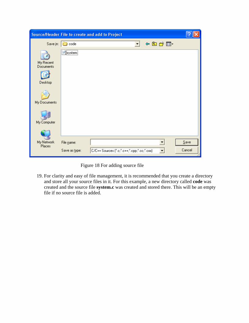
Figure 18 For adding source file
19. For clarity and easy of file management, it is recommended that you create a directory and store all your source files in it. For this example, a new directory called code was created and the source file system.c was created and stored there. This will be an empty file if no source file is added.

Figure 19 System.c
20. Expand Sources, and then double click on the system.c file to open it. All that is needed in this source file are the few lines shown above. This will print to the STDIO (UART) the phrase “Microblaze” and toggle the LED.
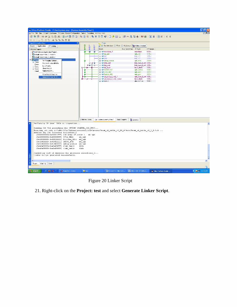
Figure 20 Linker Script
21. Right-click on the Project: test and select Generate Linker Script.

Figure 21 Memory Assignments
22. Click OK. Note The default linker script uses a fixed start address of 0x00000000 for PowerPC. Modify the start address to reflect the address corresponding to the memory defined in your hardware system. Default linker scripts assume a contiguous memory starting from the address defined as the start address. If the application cannot fit into this contiguous region, or if the application needs to be split across different memories in the system, then a custom linker script is needed. Run the Generate Linker Script command to create a custom linker script for the application.
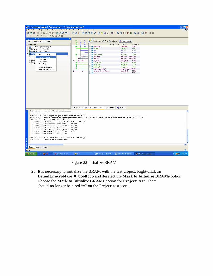
Figure 22 Initialize BRAM
23. It is necessary to initialize the BRAM with the test project. Right-click on Default:microblaze_0_bootloop and deselect the Mark to Initialize BRAMs option.
Choose the Mark to Initialize BRAMs option for Project: test. There should no longer be a red “x” on the Project: test icon.
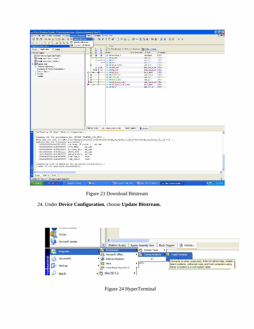
Figure 23 Download Bitstream
24. Under Device Configuration, choose Update Bitstream.
Figure 24 HyperTerminal

25. Start the HyperTerminal software. As stated above, it is necessary to have a null modem cable to communicate between the Hyper Terminal on the PC and the FPGA platform. Hyper Terminal should be configured to connect using the port assigned to the USB-to-Serial cable.
Figure 25 Port Confirmation
26. If you are unsure about which COM Port you are using, you can see by going to the Device Manager under the hardware tab. To get there, go to control panel and then system. As shown above, the USB-to-Serial adapter that is connected to this PC is connected to COM6, therefore Hyper Terminal is also configured to connect using COM6.

Figure 26 HyperTerminal Parameters
27. Choose these settings for the Hyper Terminal on the PC to conform with the settings used on the FPGA Board. Once you choose these settings, click on Apply. This will allow the user to just choose Restore Defaults each following time they launch Hyper Terminal.

Figure 27 Download Bitstream
28. If the entire software application fits on FPGA block RAM (BRAM) blocks, the system can be initialized by updating the hardware bitstream with the BRAM initialization data. This updated bitstream can then be downloaded to the FPGA. Under Device configuration, choose Download Bitstream. The bitstream is initialized with the executable. In the XPS (non-submodule) flow, this will result in the generation of the <project>/implementation/download.bit bitstream file containing both hardware and software.
29. Once the project has completed and downloaded, the HyperTerminal will display Microblaze and LED will turn on and off. .