Embed Size (px)
Citation preview
MicroBlaze Tutorial on EDK 10.1 using Sparatan III E
Behavioural Simulation of MicroBlaze System
Ahmed Elhossini
January 24, 2010
1 Introduction
1.1 Objectives
This tutorial will demonstrate process of simulating a MicroBlaze system using the Embedded DevelopmentKit (EDK) and ModelSim. ModelSim is an HDL simulation tool that is able to perform several types ofsimulations. In this tutorial we will use ModelSim to perform behavioral and timing simulations for anembedded system based on MircoBlaze. Behavioral simulation is used to test the functionality of thesystem using an abstracted model of the different component of the system. This simulation allows thedesigner to check the functionality of the system before moving to other stages of the design process.Timing simulation is performed on an HDL model of the system after completing the place and routephase. This model include a detailed information about the design. This simulation shows the behavior ofthe system when it is physically implemented on the FPGA.
1.2 System Requirements
You must have the following software installed on your PC to complete this tutorial:
• Windows 2000 SP2/Windows XP
• EDK 10.1i.
• ISE 10.1i.
• ModelSim SE 6.3c.
• Familiarity with Xilinx ISE 10.1 design flow.
• Complete the tutorial: “MicroBlaze Tutorial on EDK 10.1 using Sparatan III E”. We will use thesame MicroBlaze system for simulation in this tutorial.
Note: The design is based on the Spartan III E Starter Kit. However the board itself isnot required to complete this tutorial.
1.3 Tutorial Steps
In this tutorial, the following steps will be performed:
• Preparing the MicroBlaze system for simulation using EDK.
1

Figure 1: Open an Existing Design
• Building the behavioral simulation model for the MicroBlaze system.
• Performing behavioral simulation using ModelSim.
• Building the timing simulation model for the MicroBlaze system.
• Performing timing simulation using ModelSim.
By the end of this tutorial you will be able to simulate the EDK design using ModelSim.
2 Preparing the Design for Simulation
The first step in this tutorial is to prepare the MicoBlaze system for simulation. This involves building thesimulation library required by ModelSim to simulate EDK systems. Follow the following steps:
• Open XPS, by selecting Start → All Programs → Development → Xilinx ISE Design Suite 10.1 →EDK → Xilinx Platform Studio
• Open the design you created in the tutorial “MicroBlaze Tutorial on EDK 10.1 using Sparatan IIIE” as shown in Figure 1.
The design will be loaded as shown in Figure 2.
• Now we will start building the simulation library. Select Simulation→ Compile Simulation Libraries.This step is required only once as the simulation library can be used later to simulate any othersystem.This will start the “Simulation Library Compilation Wizard” that will be used to setup thecompilation process of the simulation library as shown in Figure 3. Click Next.
• The second screen of the wizard will be used to select the simulation software as shown in Figure 4.EDK simulation supports only two types of simulators: i) ModelSim 6.3c SE and ii) NCSim whichis not supported on windows platform. For this reason ModelSim 6.3c is used in this tutorial tosimulate MicoBlaze system. It is important to know that if ModelSim 6.3c is not installed in yoursystem, the wizard will not continue. Select ModelSim 6.3c and then Click Next.
2

Figure 2: Loaded Design
Figure 3: Simulation Library Compilation Wizard - Welcome
3

Figure 4: Simulation Library Compilation Wizard - Select Simulator
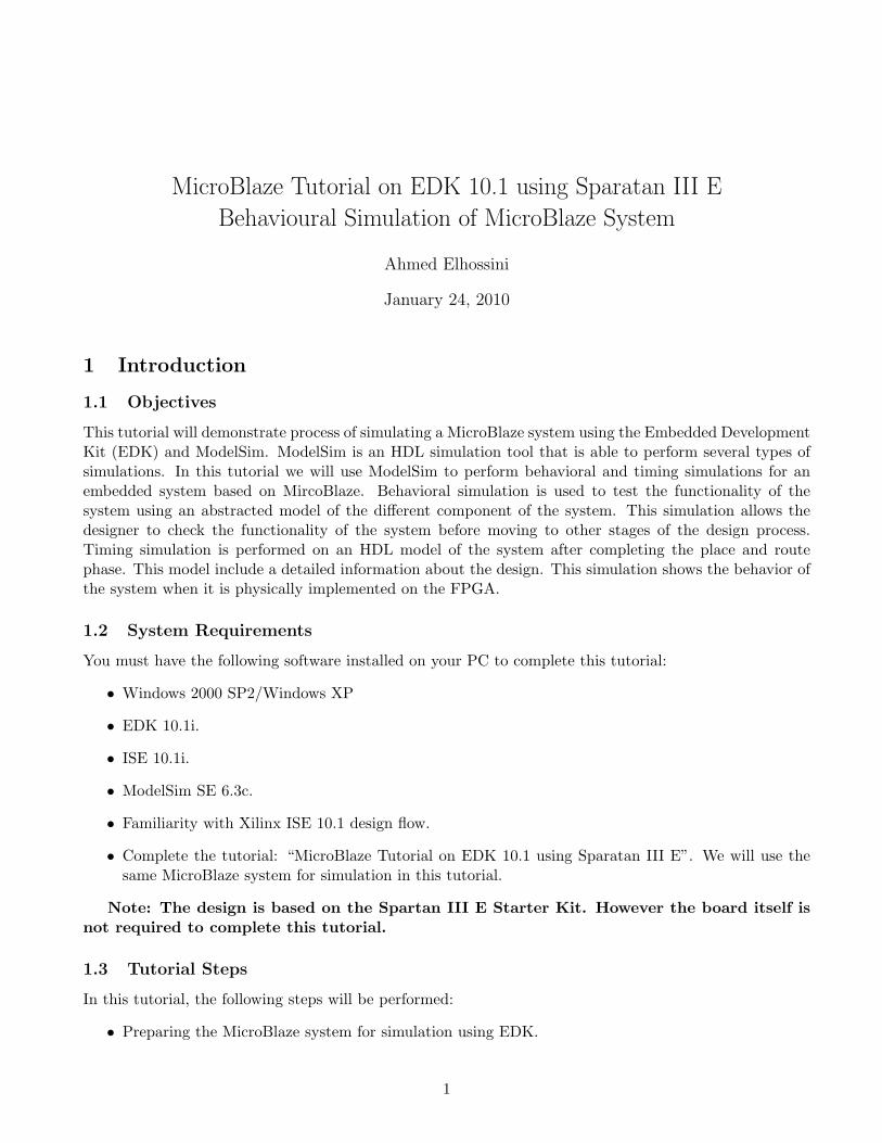
• The third screen of the wizard is used to select the HDL language used by the simulator as shown inFigure 5. ModelSim 6.3c supports both VHDL and Verilog. It is up to you to select which language,however, selecting both language will allow to use any of them if required by it will require more diskspace. Select Both VHDL and Verilog and then Click Next.
• The fourth screen of the wizard is used to select the directory in which ISE simulation models arecompiled as shown in Figure 6. You can select any location to store the library files. As mentionedearlier the library could be used by any design for simulation, so selecting the library location isimportant. Select a suitable location and Click Next.
• The next screen of the wizard is used to select the directory in which EDL simulation models arecompiled as shown in Figure 7. Select a suitable location and Click Next.
• The next screen is used to setup some options related to the EDK library as shown in Figure 8.Nothing needs to be changed in this screen. Click Next.
• The next screen of the wizard shown in Figure 9 is used for the compilation options for third par-ty/user peripherals that need to be compiled with the library. We do not have such peripherals inour design so we can move to the next screen. Click Next.
• Now the compilation process will start as shown in Figure 10. The compilation process will takesome time. When the compilation process complete the wizard window will be as shown in Figure11. When the compilation process complete, the library files will be stored in the directory specifiedin the previous steps. The files can be used later for the simulation processes by selecting thesedirectories with other designs. Click Next to continue.
• The next screen of the wizard shows some information about the simulation process in the EDK.Click Next.
• The wizard now will show the summary screen (Figure 13). This window shows the details of thecompilation process. Now the simulation library building is complete and we are ready to simulate
4
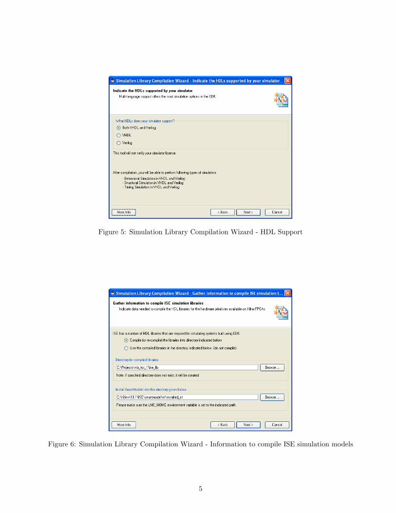
Figure 5: Simulation Library Compilation Wizard - HDL Support
Figure 6: Simulation Library Compilation Wizard - Information to compile ISE simulation models
5

Figure 7: Simulation Library Compilation Wizard - Information to compile EDK simulation models
Figure 8: Simulation Library Compilation Wizard - EDK library options
6

Figure 9: Simulation Library Compilation Wizard - Compiling other peripherals
Figure 10: Simulation Library Compilation Wizard - Compiling ISE and EDK library (start)
7

Figure 11: Simulation Library Compilation Wizard - Compiling ISE and EDK library (completed)
Figure 12: Simulation Library Compilation Wizard - Simulation Requirements
8
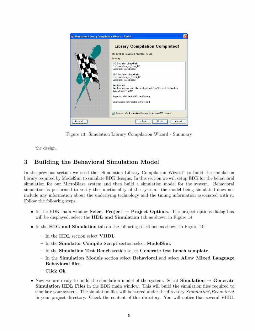
Figure 13: Simulation Library Compilation Wizard - Summary
the design.
3 Building the Behavioral Simulation Model
In the previous section we used the “Simulation Library Compilation Wizard” to build the simulationlibrary required by ModelSim to simulate EDK designs. In this section we will setup EDK for the behavioralsimulation for our MicroBlaze system and then build a simulation model for the system. Behavioralsimulation is performed to verify the functionality of the system. the model being simulated does notinclude any information about the underlying technology and the timing information associated with it.Follow the following steps:
• In the EDK main window Select Project → Project Options. The project options dialog boxwill be displayed, select the HDL and Simulation tab as shown in Figure 14.
• In the HDL and Simulation tab do the following selections as shown in Figure 14:
– In the HDL section select VHDL.
– In the Simulator Compile Script section select ModelSim.
– In the Simulation Test Bench section select Generate test bench template.
– In the Simulation Models section select Behavioral and select Allow Mixed LanguageBehavioral files.
– Click Ok.
• Now we are ready to build the simulation model of the system. Select Simulation → GenerateSimulation HDL Files in the EDK main window. This will build the simulation files required tosimulate your system. The simulation files will be stored under the directory Simulation\Behavioralin your project directory. Check the content of this directory. You will notice that several VHDL
9

Figure 14: Change Simulation Setting for Behavioral Simulation
Figure 15: Building Simulation Model Completed
10

files are created for each component of the system. The file system tb.vhdl is a test bench VHDLfile create using EDK to control the IO signals of the system during the simulation.
Open the file system tb.vhdl in the EDK window by selecting File→Open and then browse tothe file location as stated above. The contains the required VHDL code required to instantiate thesystem inside ModelSim, and two VHDL processes that provides both the clock and reset signals forthe system as shown in the following code:——————————————————————————-– system tb.vhd——————————————————————————-library IEEE;use IEEE.STD LOGIC 1164.ALL;
library UNISIM;use UNISIM.VCOMPONENTS.ALL;
entity system tb isend system tb;
architecture STRUCTURE of system tb is
constant sys clk pin PERIOD : time := 20000.000000 ps;constant sys rst pin LENGTH : time := 320000 ps;
component system isport (
fpga 0 RS232 DCE RX pin : in std logic;fpga 0 RS232 DCE TX pin : out std logic;fpga 0 LEDs 8Bit GPIO d out pin : out std logic vector(0 to 7);fpga 0 DIP Switches 4Bit GPIO in pin : in std logic vector(0 to 3);fpga 0 DDR SDRAM DDR DQS Div I DDR SDRAM DDR DQS Div O : inout std logic;fpga 0 DDR SDRAM DDR Clk pin : out std logic;fpga 0 DDR SDRAM DDR Clk n pin : out std logic;fpga 0 DDR SDRAM DDR Addr pin : out std logic vector(12 downto 0);fpga 0 DDR SDRAM DDR BankAddr pin : out std logic vector(1 downto 0);fpga 0 DDR SDRAM DDR CAS n pin : out std logic;fpga 0 DDR SDRAM DDR CE pin : out std logic;fpga 0 DDR SDRAM DDR CS n pin : out std logic;fpga 0 DDR SDRAM DDR RAS n pin : out std logic;fpga 0 DDR SDRAM DDR WE n pin : out std logic;fpga 0 DDR SDRAM DDR DM pin : out std logic vector(1 downto 0);fpga 0 DDR SDRAM DDR DQS : inout std logic vector(1 downto 0);fpga 0 DDR SDRAM DDR DQ : inout std logic vector(15 downto 0);sys clk pin : in std logic;sys rst pin : in std logic
);end component;
– Internal signals
signal fpga 0 DDR SDRAM DDR Addr pin : std logic vector(12 downto 0);signal fpga 0 DDR SDRAM DDR BankAddr pin : std logic vector(1 downto 0);signal fpga 0 DDR SDRAM DDR CAS n pin : std logic;signal fpga 0 DDR SDRAM DDR CE pin : std logic;signal fpga 0 DDR SDRAM DDR CS n pin : std logic;signal fpga 0 DDR SDRAM DDR Clk n pin : std logic;signal fpga 0 DDR SDRAM DDR Clk pin : std logic;signal fpga 0 DDR SDRAM DDR DM pin : std logic vector(1 downto 0);signal fpga 0 DDR SDRAM DDR DQ : std logic vector(15 downto 0);signal fpga 0 DDR SDRAM DDR DQS : std logic vector(1 downto 0);signal fpga 0 DDR SDRAM DDR DQS Div I DDR SDRAM DDR DQS Div O : std logic;signal fpga 0 DDR SDRAM DDR RAS n pin : std logic;signal fpga 0 DDR SDRAM DDR WE n pin : std logic;signal fpga 0 DIP Switches 4Bit GPIO in pin : std logic vector(0 to 3);signal fpga 0 LEDs 8Bit GPIO d out pin : std logic vector(0 to 7);
11

signal fpga 0 RS232 DCE RX pin : std logic;signal fpga 0 RS232 DCE TX pin : std logic;signal sys clk pin : std logic;signal sys rst pin : std logic;
begin
dut : systemport map (
fpga 0 RS232 DCE RX pin ⇒ fpga 0 RS232 DCE RX pin,fpga 0 RS232 DCE TX pin ⇒ fpga 0 RS232 DCE TX pin,fpga 0 LEDs 8Bit GPIO d out pin ⇒ fpga 0 LEDs 8Bit GPIO d out pin,fpga 0 DIP Switches 4Bit GPIO in pin ⇒ fpga 0 DIP Switches 4Bit GPIO in pin,fpga 0 DDR SDRAM DDR DQS Div I DDR SDRAM DDR DQS Div O⇒ fpga 0 DDR SDRAM DDR DQS Div I DDR SDRAM DDR DQS Div O,fpga 0 DDR SDRAM DDR Clk pin ⇒ fpga 0 DDR SDRAM DDR Clk pin,fpga 0 DDR SDRAM DDR Clk n pin ⇒ fpga 0 DDR SDRAM DDR Clk n pin,fpga 0 DDR SDRAM DDR Addr pin ⇒ fpga 0 DDR SDRAM DDR Addr pin,fpga 0 DDR SDRAM DDR BankAddr pin ⇒ fpga 0 DDR SDRAM DDR BankAddr pin,fpga 0 DDR SDRAM DDR CAS n pin ⇒ fpga 0 DDR SDRAM DDR CAS n pin,fpga 0 DDR SDRAM DDR CE pin ⇒ fpga 0 DDR SDRAM DDR CE pin,fpga 0 DDR SDRAM DDR CS n pin ⇒ fpga 0 DDR SDRAM DDR CS n pin,fpga 0 DDR SDRAM DDR RAS n pin ⇒ fpga 0 DDR SDRAM DDR RAS n pin,fpga 0 DDR SDRAM DDR WE n pin ⇒ fpga 0 DDR SDRAM DDR WE n pin,fpga 0 DDR SDRAM DDR DM pin ⇒ fpga 0 DDR SDRAM DDR DM pin,fpga 0 DDR SDRAM DDR DQS ⇒ fpga 0 DDR SDRAM DDR DQS,fpga 0 DDR SDRAM DDR DQ ⇒ fpga 0 DDR SDRAM DDR DQ,sys clk pin ⇒ sys clk pin,sys rst pin ⇒ sys rst pin
);
– Clock generator for sys clk pin
process
begin
sys clk pin ⇐ ’0’;
loop
wait for (sys clk pin PERIOD/2);
sys clk pin ⇐ not sys clk pin;
end loop;
end process;
– Reset Generator for sys rst pin
process
begin
sys rst pin ⇐ ’1’;
wait for (sys rst pin LENGTH);
sys rst pin ⇐ not sys rst pin;
wait;
end process;
– START USER CODE (Do not remove this line)
– User: Put your stimulus here. Code in this
– section will not be overwritten.
12

Figure 16: Modelsim Started
– END USER CODE (Do not remove this line)
end architecture STRUCTURE;
configuration system tb conf of system tb is
for STRUCTURE
for all : system
use configuration work.system conf;
end for;
end for;
end system tb conf;
This code can be modified to add customized simulation scenarios for the system. We do not need tomodify the code as it generates all the signals required to run the system (clock and reset signals).
4 Behavioral Simulation
In the previous section we used EDK to generate a simulation model for our design. Now we are ready touse ModelSim to perform behavioral simulation. Select Simulation→ Launch HDL Simulator. Thiswill start ModelSim as shown in Figure 16. The ModelSim main window contains several windows at startup.
The transcript window is used to enter ModelSim commands that are used to control the simulation.EDK simulator script define five commands to simulate EDK systems and a help window is displayed inthe transcript window as shown below:
13

# **********************************************************************
# **********************************************************************
# ***
# *** Simulation Setup Macros (system setup.do)
# ***
# *** c ⇒ compile the design by running the EDK compile script.
# *** Assumes ISE and EDK libraries were compiled earlier
# *** for ModelSim. (see system.do)
# ***
# *** s ⇒ load the design for simulation. (ModelSim ’vsim’
# *** command with ’system tb’) After loading the design,
# *** set up signal displays (optional) and run the simulation.
# *** (ModelSim ’run’ command)
# ***
# *** l ⇒ set up signal list display and launch a list window.
# *** ModelSim ’add -list’ commands are found in * list.do
# *** scripts. (see system list.do)
# ***
# *** w ⇒ set up signal wave display and launch a waveform window.
# *** ModelSim ’add -wave’ commands are found in * wave.do
# *** scripts. (see system wave.do)
# ***
# *** h ⇒ print this message
# ***
# **********************************************************************
# **********************************************************************
• In the transcript window enter the command “c” at the command line. This will compile the designwhich will take sometime. Then enter the command “s” which loads the design in ModelSim. Afterloading the design, the different component of the design are shown in the Workspace window asshown in Figure 17 and the Objects windows show the internal signals of any selected component.
• Enter the command “w” to load the waveform that will display some signals defined by the simulationscript generated by EDK. In behavioral simulation, the simulation scripts displays all input/outputsignals of each component in the system and the designer can add any other signal if required.
• Enter the command run 1 ms. This will start the simulation of the MicroBlaze system for 1 ms.After the simulation complete the waveform window will show the changes in all the selected signalsof the system. Clock the Plus button at the top right corner of the waveform window to maximizethe view. The results should look like Figure 19.
You can go through different signals and watch activity on each signal. For example the signalfpga 0 RS232 DCE TX pin is the serial output of the system. The activities on this signal iscorresponding the output of the software running on MicroBlaze as the standard output of thesystem is configured to use the RS232 interface (refer to the tutorial “MicroBlaze Tutorial on EDK10.1 using Sparatan III E”).
14

Figure 17: Modelsim - Design Compiled and Loaded
Figure 18: Modelsim - Loading the Waveform Window
15

Figure 19: Modelsim - Simulation Output
5 Building the Timing Simulation Model
In the previous sections we performed behavioral simulation for a MicroBlaze system using ModelSim. Wecan use this simulation to verify the functionality of the system specially in the case of a custom hardwarebeing implemented. In this section we are going to perform timing simulation which is performed using asimulation model generated from the post place and route net-list. This include all the timing informationabout the underlying technology (in our case it will include the timing information of Spartan III E FPGA).
• The first step is to change the simulation setting for timing simulation by selecting Project→ProjectOptions. Select HDL and Simulation tab and in the Simulation Models section select Timingas shown in Figure 20 and then Click Ok.
• Build the timing simulation model by selecting Simulation→ Generate Simulation HDL Files.The process will take sometime and then the EDK console window will show a message to indicatethe completion of the process as shown in Figure 21.
6 Timing Simulation
The simulation scripts generated for ModelSim define the same menu discussed earlier to control thesimulation process. Execute the commands “c” and “s” to compile and load the design. When thedesign is loaded as shown in Figure 22 all the components in the simulation model are displayed in theWorkspace Window. Compare the components tree of the timing simulation model to the behavioralsimulation model (see Figure 17).
Execute the command “w” to load the waveform. The timing simulation model is extracted from thepost place and route net-list. For this reason the information about the internal signals of each componentare different and so are not included in the waveform (compare this to the behavioral model waveform).
16

Figure 20: Change Simulation Setting for Timing Simulation
Figure 21: Building Simulation Model Completed
17

Figure 22: Modelsim - Design Compiled and Loaded
Figure 23: Modelsim - Loading the Waveform Window
18

Figure 24: Modelsim - Simulation Output
Start the simulation by executing the command run 1 ms. The timing simulation will start. Noticethat the timing simulation will take much longer time compared to the behavioral simulation. That isbecause the timing simulation model contains more information about the internal structure of the systemand technology being used to implement the system (Spartan III E FPGA). The resulting waveform shouldlook like Figure 24.
Compare the resulting waveform of the timing simulation to waveform of the behavioral simulation(Figure 19). Notice the timing differences in each input/output signals of the system. The results ofthe timing simulation is the closest to the actual implementation on board. If simulation results showsomething wrong in the system performance, this will be the same when the system is implemented on theboard.
7 Summary
In this tutorial we performed both behavioral and timing simulation for a MicroBlaze system. We usedModelSim 6.3c SE to perform both types of simulation after creating a simulation library using EDK.Behavioral simulation allows the designer to verify the functionality of the system while timing simulationallows the designer to investigate timing related issues and verify the functionality of the system on aspecific technology.
19