Embed Size (px)
Citation preview
February 8, 2002 www.xilinx.com 11-800-255-7778
R
Tutorial
Designing Custom OPB SlavePeripherals for MicroBlaze
SummaryThis document offers recommended guidelines and practices for RTL designers to createcustom OPB slave peripherals for MicroBlaze embedded systems. An introduction to On-chip Peripheral Bus (OPB) signals, basic transactions and tips for RTL coding are discussedhere.
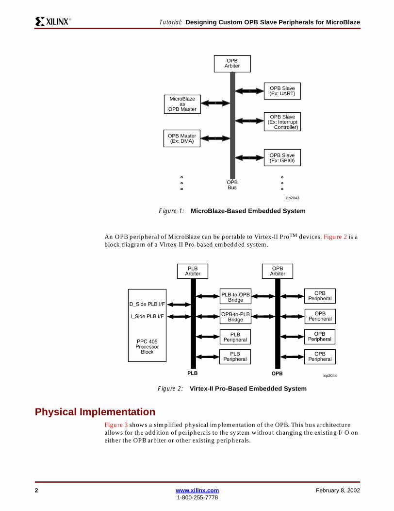
OverviewIn an embedded system design, the peripherals (for example, timers, DMA, interruptcontroller, custom applications, etc.) must be connected to the microprocessor using thedata and address buses. The complexity of system-on-chip (SOC) devices makesstandardizing the connection of different macro cells one of the top priorities in defining anembedded system. Xilinx MicroBlaze have implemented IBM's CoreConnect architecture.Ultimately, designing a complex chip based on existing intellectual property and designreuse methodology could become a straightforward task.
On-chip Peripheral Bus (OPB) version 2.1 of CoreConnect architecture is designed for easyconnection of on-chip peripheral devices. Any custom peripheral that connects to the OPBbus must meet the principles of the OPB protocol and the design must meet therequirements of Platform Generator and CoreGen flow to take advantage of the simpleautomated flow that generates the system-level architecture as well as other templatescripts supported by Xilinx.
FeaturesPlatform Generator supports the following features of on-chip peripherals and is a subsetof OPB v2.1 features:
• Fully synchronous single clock edge• 32-bit address bus, 32-bit data bus
• Single-cycle transfer of data between OPB master and OPB slave• Supports master byte enables
• Supports slave timeout suppress• Supports slave retry
• No tristate drivers required
Note that the dynamic bus sizing feature is not supported in OPB v2.1.
Figure 1 is a block diagram of a MicroBlaze-based embedded system.
2 www.xilinx.com February 8, 20021-800-255-7778
Tutorial: Designing Custom OPB Slave Peripherals for MicroBlazeR
An OPB peripheral of MicroBlaze can be portable to Virtex-II ProTM devices. Figure 2 is ablock diagram of a Virtex-II Pro-based embedded system.
Physical ImplementationFigure 3 shows a simplified physical implementation of the OPB. This bus architectureallows for the addition of peripherals to the system without changing the existing I/O oneither the OPB arbiter or other existing peripherals.
Figure 1: MicroBlaze-Based Embedded System
Figure 2: Virtex-II Pro-Based Embedded System
OPBArbiter
OPB Slave(Ex: UART)
OPB Slave(Ex: Interrupt
Controller)
OPB Slave(Ex: GPIO)
OPB Master(Ex: DMA)
MicroBlazeas
OPB Master
OPBBus
xip2043
OPBArbiter
PLBArbiter
PPC 405Processor
Block
OPBPeripheral
OPBPeripheral
OPBPeripheral
OPBPeripheral
PLB-to-OPBBridge
OPB-to-PLBBridge
PLBPeripheral
PLBPeripheral
D_Side PLB I/F
I_Side PLB I/F
PLB OPB xip2044

February 8, 2002 www.xilinx.com 31-800-255-7778
Interface SignalsR
The module opb_v20 in the diagram implements the OR gates defined by the OPB v2.1specification. Based on the Microprocessor Hardware Specification file (MHS) provided bythe user, Platform Generator counts the number of devices (both masters and slaves)attached to the OPB, instantiates opb_v20, and automatically connects the address bus,data buses, control and arbitration signals. The Platform Generator flow allows the user tofocus on designing the peripherals without having to worry about the system-levelconnections.
Note that all masters and slaves in the system must drive data buses to zero when they areinactive, and this has to be done internally within masters and slaves.
OPB supports multiple master devices as shown in the diagram above. Therefore, anarbiter is required to arbitrate the bus ownerships between masters. If there is only oneOPB master in the system, the OPB arbiter can still be included in the system, since thearbiter also asserts the OPB time-out signal if a slave response is not detected within 16clock cycles.
Interface SignalsThe interface signals are usually defined in the early design stages, with some adjustmentsmade in the later stages. This section lists the signals required for the OPB slave and
Figure 3: Physical Implementation of OPB in MicroBlaze System
OPBMaster
Device 1
m1m_dbus
m1m_request
mi_opb_mgrant
m1m_abus
opb_dbus
OPBMaster
Device 2
OPBArbiter
m2m_abus
m2m_request
opb_dbus
m2m_dbus
m2opb_mgrant
opb_v20
OPBSlave
Device 1
OPBSlave
Device 2
AND gateor
FDRE
opb_abus
opb_dbus
s1s_dbuss2s_dbus
AND gateor
FDRE
xip2045

4 www.xilinx.com February 8, 20021-800-255-7778
Tutorial: Designing Custom OPB Slave Peripherals for MicroBlazeR
includes optional signals for reference. Figure 4 shows the OPB Slave Interface and Table 1lists and describes the Global Signals.
Figure 4: OPB Slave Interface
Table 1: Global Signals
SignalName
Direction Width Description
OPB_Clk Input 1 All signals on the OPB are active high and are eitherdirect output of edge-triggered latches which areclocked by the OPB_Clk or are derived from theoutput of a register using several levels ofcombinatorial logic. All input signals should becaptured in the OPB masters or OPB slaves on therising edge of the OPB_Clk.
OPB_Rst Input 1 The active high reset vector is asynchronous to theOPB_Clk. The same reset signal also goes toMicroBlaze core reset.
OPBSlave
<Sln>_errAck
<Sln>_retry
<Sln>_DBus
<Sln>_xferAck
<Sln>_toutSup
OPB_RNW
OPB_seqAddr
OPB_ABus
OBP_select
OPB_BE
OPB_DBus
OPBBus
Logic
xip2046
February 8, 2002 www.xilinx.com 51-800-255-7778
Interface SignalsR
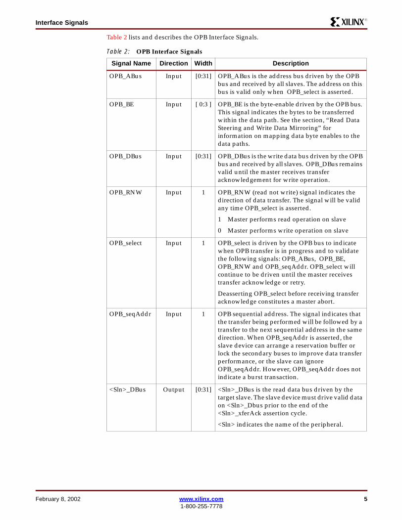
Table 2 lists and describes the OPB Interface Signals.
Table 2: OPB Interface Signals
Signal Name Direction Width Description
OPB_ABus Input [0:31] OPB_ABus is the address bus driven by the OPBbus and received by all slaves. The address on thisbus is valid only when OPB_select is asserted.
OPB_BE Input [ 0:3 ] OPB_BE is the byte-enable driven by the OPB bus.This signal indicates the bytes to be transferredwithin the data path. See the section, “Read DataSteering and Write Data Mirroring” forinformation on mapping data byte enables to thedata paths.
OPB_DBus Input [0:31] OPB_DBus is the write data bus driven by the OPBbus and received by all slaves. OPB_DBus remainsvalid until the master receives transferacknowledgement for write operation.
OPB_RNW Input 1 OPB_RNW (read not write) signal indicates thedirection of data transfer. The signal will be validany time OPB_select is asserted.
1 Master performs read operation on slave
0 Master performs write operation on slave
OPB_select Input 1 OPB_select is driven by the OPB bus to indicatewhen OPB transfer is in progress and to validatethe following signals: OPB_ABus, OPB_BE,OPB_RNW and OPB_seqAddr. OPB_select willcontinue to be driven until the master receivestransfer acknowledge or retry.
Deasserting OPB_select before receiving transferacknowledge constitutes a master abort.
OPB_seqAddr Input 1 OPB sequential address. The signal indicates thatthe transfer being performed will be followed by atransfer to the next sequential address in the samedirection. When OPB_seqAddr is asserted, theslave device can arrange a reservation buffer orlock the secondary buses to improve data transferperformance, or the slave can ignoreOPB_seqAddr. However, OPB_seqAddr does notindicate a burst transaction.
<Sln>_DBus Output [0:31] <Sln>_DBus is the read data bus driven by thetarget slave. The slave device must drive valid dataon <Sln>_Dbus prior to the end of the<Sln>_xferAck assertion cycle.
<Sln> indicates the name of the peripheral.
6 www.xilinx.com February 8, 20021-800-255-7778
Tutorial: Designing Custom OPB Slave Peripherals for MicroBlazeR
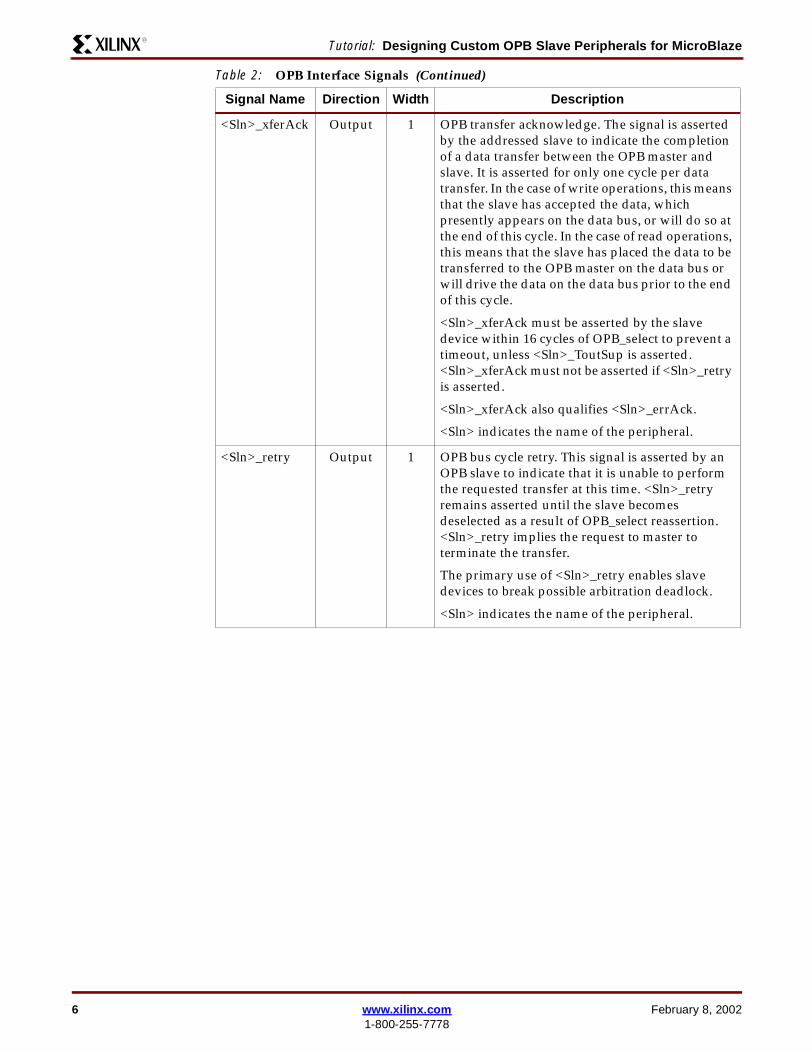
<Sln>_xferAck Output 1 OPB transfer acknowledge. The signal is assertedby the addressed slave to indicate the completionof a data transfer between the OPB master andslave. It is asserted for only one cycle per datatransfer. In the case of write operations, this meansthat the slave has accepted the data, whichpresently appears on the data bus, or will do so atthe end of this cycle. In the case of read operations,this means that the slave has placed the data to betransferred to the OPB master on the data bus orwill drive the data on the data bus prior to the endof this cycle.
<Sln>_xferAck must be asserted by the slavedevice within 16 cycles of OPB_select to prevent atimeout, unless <Sln>_ToutSup is asserted.<Sln>_xferAck must not be asserted if <Sln>_retryis asserted.
<Sln>_xferAck also qualifies <Sln>_errAck.
<Sln> indicates the name of the peripheral.
<Sln>_retry Output 1 OPB bus cycle retry. This signal is asserted by anOPB slave to indicate that it is unable to performthe requested transfer at this time. <Sln>_retryremains asserted until the slave becomesdeselected as a result of OPB_select reassertion.<Sln>_retry implies the request to master toterminate the transfer.
The primary use of <Sln>_retry enables slavedevices to break possible arbitration deadlock.
<Sln> indicates the name of the peripheral.
Table 2: OPB Interface Signals (Continued)
Signal Name Direction Width Description

February 8, 2002 www.xilinx.com 71-800-255-7778
Interface SignalsR
Table 3 lists and describes the optional Interrupt Signals.
Xilinx provides scalable Interrupt Controller, which is included in MicroBlazedevelopment kits, to support different styles of interrupts: level sensitive, edge sensitive,active high, or active low. Custom OPB peripheral applications may have differentinterrupt styles and/or multiple interrupt signals. Table 4 lists and describes the optionalApplication Signals.
<Sln>_toutSup Output 1 Slave time-out suppress. The signal is asserted byan OPB slave to indicate that the bus operation willbe delayed for an extended time. This signal mustbe asserted within 16 clock cycles from theassertion of OPB_select to prevent a bus timeout.
<Sln>_ToutSup will be used by the OPB Arbiter todisable the timeout counter and suppress theassertion of OPB_timeout. <Sln>_ToutSup mustremain asserted until the slave can complete therequested operation. Note: If the master deassertsOPB_select prior to the slave asserting<Sln>_xferAck or <Sln>_retry, thereby abortingthe transfer request, the Sln_toutSup signal mayremain asserted for one additional clock cycle.
<Sln> indicates the name of the peripheral.
<Sln>_errAck Output 1 OPB transfer error acknowledge. The signal isasserted by a slave device to indicate that the slaveencountered an error in performing the requestedtransfer. <Sln>_errAck may be assertedimmediately upon a slave device's decode of itsaddress during a transfer cycle (OPB_selectasserted) or any time thereafter. It must be validwhen <Sln>_xferAck is asserted. Slaves mustdrive their <Sln>_errAck signal only whenselected; otherwise, the slave must keep its<Sln>_errAck signal deasserted.
<Sln> indicates the name of the peripheral.
Note: All inactive OPB slave devices should drive buses to zero.
Table 3: Interrupt Signals (Optional)
Signal Name Direction Width Description
Example:
Interrupt
Output Definedby User
An OPB slave device can implement one ormultiple interrupt signals, depending onthe system requirements.
Table 4: Application Signals (Optional)
Signal Name Direction Width Description
Defined by User Definedby User
Definedby User
Defined by User
Table 2: OPB Interface Signals (Continued)
Signal Name Direction Width Description

8 www.xilinx.com February 8, 20021-800-255-7778
Tutorial: Designing Custom OPB Slave Peripherals for MicroBlazeR
Each application has application-specific signals, including RX and TX in UART designsand Sda (Serial Data) and Scl (Serial Clock) in IIC designs.
In the module level of HDL design, ports should be defined either as input or output.Thus, users should expand a bidirectional (inout) port to 3 separate ports: 2 outputs and 1input. The 2 outputs will be the output port and the tristate (enable) port of the inout. Theinput will be the input port to the inout. The names may correspond to the convention<ioname>_T, <ioname>_O, and <ioname>_I, where <ioname> can be your bidirectionalsignal name; for example, GPIO_T, GPIO_O and GPIO_I.
Generics (Optional)It is recommended that generics be used, rather than hard-coded values, to make thedesign reusable and retargetable. For example, generics can be used in the baud rate anddata bit for the UART, the time interval for the watchdog timer, etc. Therefore, when thespecification of a peripheral has to be updated, the user can easily modify the genericswithout changing the source code.
Notice that Platform Generator has keywords towards attributes names. PlatformGenerator does automatic expansion on certain reserved attributes, such asC_OPB_DWIDTH and C_OPB_AWIDTH. Therefore, users will have to refer to thePlatform Generator reference guide for the list of reserved attribute names. Table 5 listsand describes the optional Generic Names.
Table 5: Generics (Optional)
Generic Name Type Width Description
C_BASEADDR std_logic_vector [0:31] The base address of this memory-mapped slave device. When amaster initiates an operation byasserting OPB_select, the addressdecode logic may reference thisvalue and compare with OPB_ABusto determine whether this slave hasbeen targeted by the master.
C_BASEADDR is a keywordattribute for Platform Generator.
C_HIGHADDR std_logic_vector [0:31] The high address of this memory-mapped slave device. Together withthe base address, the total memoryspace is defined.
C_HIGHADDR is a keywordattribute for Platform Generator.
C_OPB_DWIDTH integer - OPB System data bus width.
MicroBlaze employs 32 2-bit OPBarchitecture, so this value should befixed to 32.
C_OPB_AWIDTH integer - OPB System address bus width.
MicroBlaze employes 32-bit OPBarchitecture, so this value should befixed to 32.
Others
(Defined by User)
- - -

February 8, 2002 www.xilinx.com 91-800-255-7778
Generic Block DiagramR
Generic Block DiagramAn OPB slave design example consists of the following components:
• Address decoding logic
• OPB slave interface logic• Application-specific logic
Figure 5 is a block diagram example for an OPB Slave.
Address Decoding LogicEach OPB slave device should have its own address decoding logic. When OPB_select isasserted and OPB_ABus is valid, all OPB slave devices will decode the coming address anddetermine whether to respond or to ignore. If OPB slave devices are not targeted by themaster which has been granted the ownership of the bus, the slaves must output all zerosfor all OPB-related interface signals. The user will want to make sure there is no overlap inmemory-mapped space allocation. Otherwise, multiple OPB slave devices may try torespond to the same transaction, leading to system malfunctions.
Since address decoding logic sometimes is a critical path for timing, the MicroBlazedevelopment kit provides a sample for parameterizable peripheral address decoding logicwritten in VHDL. The file is named pselect.vhd. The file pselect.vhd is a general-purposedecoding logic targeting Xilinx FPGA families for best area and timing optimization. Thismodule can also be reused in bus systems other than the OPB system. If this file is notavailable in the development kit, users can always design a simple comparator todetermine address.
Figure 5: A Block Diagram Example for an OPB Slave
OPB_ABusOPB_select
Addr match(Peripheral select)
OPB_DBus
OPB_BE
Application-specific
logic
REG
FDRE
REG<Sln>_DBus
<Sln>_xferAck
Applications
Read data
Address decoding logic(EX: pslect.vhd)
OPB SlaveI/F logicREG
OPBBus
QDR xfer_Ack
xip2047

10 www.xilinx.com February 8, 20021-800-255-7778
Tutorial: Designing Custom OPB Slave Peripherals for MicroBlazeR
Table 6 shows the generics and I/O interface of pselect.vhd. Note that pselect utilizespurely combinatorial logic and the user must analyze the timing arch through pselect andregister the output signal “PS” prior to use, if necessary.
Table 7 shows the I/O signal names of the interface of pselect.vhd.
OPB Slave Interface LogicOnce the slave has decoded its address and determined to respond to the transaction, thisOPB slave interface logic handles the handshake, protocol, etc. See “Interface Signals andthe Timing Diagram” for further details.
Application-Specific LogicFor each application, application-specific logic must be defined by the user.
Table 6: Generics of pselect.vhd
GenericName
Type Width Description
C_AB Integer - Number of the most significant bit on theaddress bus to be decoded. If C_AB gets largervalue, more bits must be compared with inputaddress. In this case, less memory-mappedspace is defined for this slave peripheral.
C_AW Integer - Width of the input address bus. InMicroBlaze’s current MDT flow, C_AWshould have a fixed value of 32.
C_BAR std_logic_vector 32 Base address of this slave peripheral. Whenthe C_AB most significant address bits matchthe C_AB most significant C_BAR bits, PS(peripheral select) is asserted.
Table 7: I/O Interface of pselect.vhd
Signal Name Direction Width Description
A Input [0:C_AW-1] Address input. In the OPB subsystem,this should be connected to OPB_ABus,or a registered input of OPB_ABus,depending on timing requirement.
Avalid Input 1 Address valid. In the OPB subsystem,this should be connected to OPB_select,or a registered input of OPB_select,depending on the timing requirement.
PS Output 1 Peripheral select. When the C_AB mostsignificant address bits match the C_ABmost significant C_BAR bits, PS isasserted. As PS is not a registered outputfrom pselect.vhd, the user must registerthis signal before using it.

February 8, 2002 www.xilinx.com 111-800-255-7778
Timing DiagramR
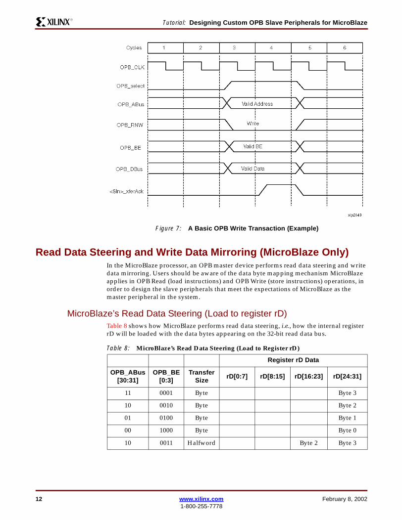
Timing DiagramFigure 6 shows basic OPB read transactions and Figure 7 shows basic OPB writetransactions. The OPB master asserts OPB_select and puts valid OPB_ABus, OPB_BE andOPB_RNW on the buses. The slave completes the transfer by asserting OPB_xferAck,which causes the master to latch data from the data bus on read transfers, and deassertselect.
Note that the cycles for the OPB master device asserting its request to the OPB arbiter is notshown in these diagrams. Also refer to OPB 2.1 Specification from IBM for other protocoldefinition.
Figure 6: A Basic OPB Read Transaction (Example)
12 www.xilinx.com February 8, 20021-800-255-7778
Tutorial: Designing Custom OPB Slave Peripherals for MicroBlazeR
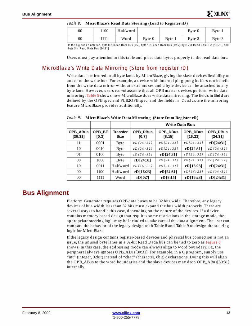
Read Data Steering and Write Data Mirroring (MicroBlaze Only)In the MicroBlaze processor, an OPB master device performs read data steering and writedata mirroring. Users should be aware of the data byte mapping mechanism MicroBlazeapplies in OPB Read (load instructions) and OPB Write (store instructions) operations, inorder to design the slave peripherals that meet the expectations of MicroBlaze as themaster peripheral in the system.
MicroBlaze’s Read Data Steering (Load to register rD)Table 8 shows how MicroBlaze performs read data steering, i.e., how the internal registerrD will be loaded with the data bytes appearing on the 32-bit read data bus.
Figure 7: A Basic OPB Write Transaction (Example)
Table 8: MicroBlaze’s Read Data Steering (Load to Register rD)
Register rD Data
OPB_ABus[30:31]
OPB_BE[0:3]
TransferSize
rD[0:7] rD[8:15] rD[16:23] rD[24:31]
11 0001 Byte Byte 3
10 0010 Byte Byte 2
01 0100 Byte Byte 1
00 1000 Byte Byte 0
10 0011 Halfword Byte 2 Byte 3
February 8, 2002 www.xilinx.com 131-800-255-7778
Bus AlignmentR
Users must pay attention to this table and place data bytes properly to the read data bus.
MicroBlaze’s Write Data Mirroring (Store from register rD)Write data is mirrored to all byte lanes by MicroBlaze, giving the slave devices flexibility toattach to the write bus. For example, a device with internal ping-pong buffers can benefitfrom the write data mirror without extra muxes and a byte device can be attached to anybyte lane. However, users cannot assume that all OPB master devices perform write datamirroring. Table 9 shows how MicroBlaze does write data mirroring. The fields in Bold aredefined by the OPB spec and PLB2OPB spec, and the fields in Italic are the mirroringfeature MicroBlaze provides additionally.a
Bus AlignmentPlatform Generator requires OPB data buses to be 32 bits wide. Therefore, any legacydevices of bus width less than 32 bits must expand the bus width properly. There areseveral ways to handle this case, depending on the nature of the devices. If a devicecontains memory based design that requires some restrictions in the storage mode, theappropriate steering logic may be included to take care of the data alignment. The user cancompare the behavior of the legacy design with Table 8 and Table 9 to design the steeringlogic for MicroBlaze.
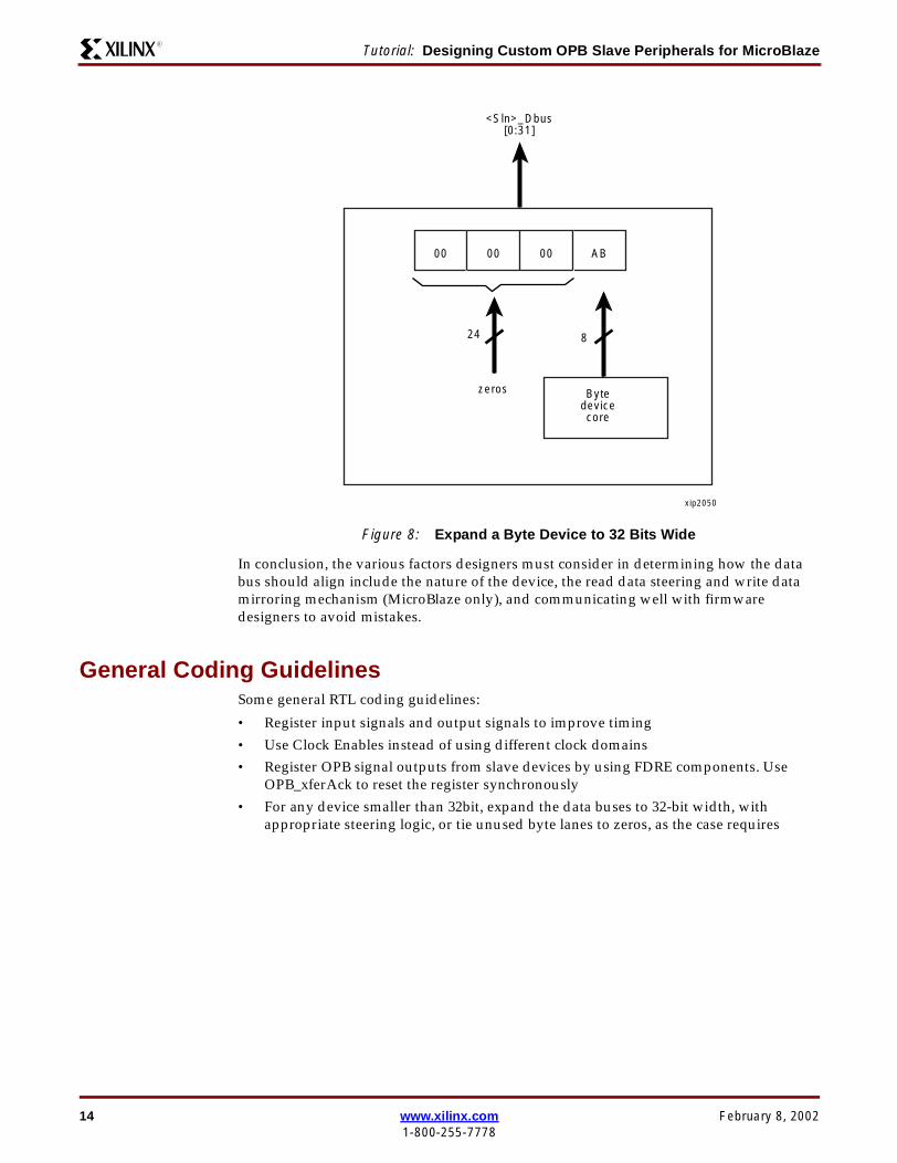
If the legacy design contains register-based devices and physical bus connection is not anissue, the unused byte lanes in a 32-bit Read Dada bus can be tied to zero as Figure 8shows. In this case, the addressing mode can always align to word boundary, i.e., theperipheral always ignores OPB_ABus[30:31]. For example, in a C program, simply use“int” (integer, 32bit) instead of “char” (character, 8bit) declarations. Doing this will alignthe OPB_ABus to the word boundaries and the slave devices may drop OPB_ABus[30:31]internally.
00 1100 Halfword Byte 0 Byte 1
00 1111 Word Byte 0 Byte 1 Byte 2 Byte 3In the big endian notation, byte 0 is Read Data Bus [0:7], byte 1 is Read Data Bus [8:15], byte 2 is Read Data Bus [16:23], andbyte 3 is Read Data Bus [24:31].
Table 8: MicroBlaze’s Read Data Steering (Load to Register rD)
Table 9: MicroBlaze’s Write Data Mirroring (Store from Register rD)
Write Data Bus
OPB_ABus[30:31]
OPB_BE[0:3]
TransferSize
OPB_DBus[0:7]
OPB_DBus[8:15]
OPB_DBus[16:23]
OPB_DBus[24:31]
11 0001 Byte rD[24:31] rD[24:31] rD[24:31] rD[24:31]10 0010 Byte rD[24:31] rD[24:31] rD[24:31] rD[24:31]
01 0100 Byte rD[24:31] rD[24:31] rD[24:31] rD[24:31]
00 1000 Byte rD[24:31] rD[24:31] rD[24:31] rD[24:31]
10 0011 Halfword rD[16:23] rD[24:31] rD[16:23] rD[24:31]00 1100 Halfword rD[16:23] rD[24:31] rD[16:23] rD[24:31]
00 1111 Word rD[0:7] rD[8:15] rD[16:23] rD[24:31]
14 www.xilinx.com February 8, 20021-800-255-7778
Tutorial: Designing Custom OPB Slave Peripherals for MicroBlazeR
In conclusion, the various factors designers must consider in determining how the databus should align include the nature of the device, the read data steering and write datamirroring mechanism (MicroBlaze only), and communicating well with firmwaredesigners to avoid mistakes.
General Coding GuidelinesSome general RTL coding guidelines:
• Register input signals and output signals to improve timing
• Use Clock Enables instead of using different clock domains• Register OPB signal outputs from slave devices by using FDRE components. Use
OPB_xferAck to reset the register synchronously
• For any device smaller than 32bit, expand the data buses to 32-bit width, withappropriate steering logic, or tie unused byte lanes to zeros, as the case requires
Figure 8: Expand a Byte Device to 32 Bits Wide
zeros
<Sln>_Dbus[0:31]
00 00 00 AB
24 8
Bytedevicecore
xip2050

February 8, 2002 www.xilinx.com 151-800-255-7778
General Coding GuidelinesR
The next section uses MYGPIO as a design example, based on the topics discussed in thepreceding sections. MYGPIO is a simple peripheral consisting of three memory-mappedregisters for software access. Figure 9 shows the block diagram for MYGPIO.
entity MYGPIO isgeneric (C_OPB_AWIDTH : integer := 32;C_OPB_DWIDTH : integer := 32;C_BASEADDR : std_logic_vector(0 to 31) := X"FFFF_8000";C_HIGHADDR : std_logic_vector(0 to 31) := X"FFFF_80FF");
port (-- Global signals
OPB_Clk : in std_logic;OPB_Rst : in std_logic;
Interrupt : out std_logic;
-- OPB signalsOPB_ABus : in std_logic_vector(0 to C_OPB_AWIDTH-1);OPB_BE : in std_logic_vector(0 to C_OPB_DWIDTH/8-1);OPB_DBus : in std_logic_vector(0 to C_OPB_DWIDTH-1);OPB_RNW : in std_logic;OPB_select : in std_logic;OPB_seqAddr : in std_logic;
GPIO_DBus : out std_logic_vector(0 to C_OPB_DWIDTH-1);GPIO_errAck : out std_logic;GPIO_retry : out std_logic;GPIO_toutSup : out std_logic;GPIO_xferAck : out std_logic;
-- GPIO signalsGPIO_IO_I : in std_logic_vector(0 to 7); --GPIO inputGPIO_IO_O : out std_logic_vector(0 to 7); --GPIO outputGPIO_IO_T : out std_logic_vector(0 to 7) --GPIO tri-state ouput);
end entity MYGPIO;
Figure 10 shows the entity declaration that describes the interface of the design to itsexternal environment. In the generic declaration, C_OPB_AWIDTH and C_OPB_DWIDTH
Figure 9: Block Diagram for MYGPIO
Figure 10: Entity of MYGPIO
OPBI/F
Offset x00GPIO/I
Offset x04GPIO/O
Offset x08GPIO/T
GPIO
MYGPIOOPB
xip2151

16 www.xilinx.com February 8, 20021-800-255-7778
Tutorial: Designing Custom OPB Slave Peripherals for MicroBlazeR
define the width for address bus and data buses. The parameterized coding style providesmore flexibility to target different bus standards for future expansion. In the MicroBlazesystem, since dynamic bus sizing is not supported and Platform Generator supports 32-bitaddress and data buses, C_OPB_AWIDTH and C_OPB_DWIDTH should be 32.
C_BASEADDR and C_HIGHADDR define the memory-mapped space for MYGPIO in theembedded system defined by the user.
The port declaration uses:
• Global signals: OPB_Clk and OPB_Rst• OPB signals: OPB_ABus, OPB_BE, OPB_RNW, OPB_select, OPB_seqAddr,
OPB_DBus, GPIO_DBus, GPIO_errAck, GPIO_retry, GPIO_toutSup, GPIO_xferAck
• GPIO signals: GPIO_IO_I, GPIO_IO_O, and GPIO_IO_T
The width of GPIO_DBus (the read bus output from MYGPIO) is 32 bits wide, even thoughMYGIPO has an 8-bit core. In this example, only GPIO_DBus[24:31] is used, whileGPIO_DBus[0:23] is tied to zero. Platform Generator requires that all OPB address andOPB read/write data buses in the VHDL entity be to std_logic_vector (0 to 31).
Figure 11 is an example VHDL code utilizing all the topics discussed in the precedingsections.
architecture RTL of MYGPIO is
-- Special function to calculate number of bits need to be decoded-- based on C_BASEADDR and C_HIGHADDR.-- If C_BASEADDR = X"FFFF_8000" and C_HIGHADDR = X"FFFF_80FF",-- the function returns 24.
function Addr_Bits (x, y : std_logic_vector(0 to C_OPB_AWIDTH-1))return integer is
variable addr_nor : std_logic_vector(0 to C_OPB_AWIDTH-1);begin
addr_nor := x xor y;for i in 0 to C_OPB_AWIDTH-1 loop
if addr_nor(i) = '1' then return i;end if;
end loop;return(C_OPB_AWIDTH);
end function Addr_Bits;
constant C_AB : integer:= Addr_Bits(C_OPB_HIGHADDR, C_OPB_BASEADDR);
...
...
begin -- architecture RTL
------------------------------------------------------------------- Handling the OPB bus interface-----------------------------------------------------------------
-- OPB address decoding using pselect.vhd.-- The generic map C_BASEADDR is passed from entity,-- C_AB is the return value from function Addr_Bits().-- If C_AB gets smaller, the logic of pselect gets smaller.---- OPB_ABus and OPB_select come from the ports.-- gpio_CS will be registered prior to usage.-- Use OPB_ABus_reg and OPB_select_reg if non-registered-- signals don’t meet timing.
pselect_I : pselectgeneric map (
C_AB => C_AB,

February 8, 2002 www.xilinx.com 171-800-255-7778
General Coding GuidelinesR
C_AW => OPB_ABus'length,C_BAR => C_BASEADDR)
port map (A => OPB_ABus,AValid => OPB_select,ps => jtag_UART_CS);
-- First register gpio_CS generated by pselect-- uart_CS_1_DFF is synchronously reseted by xfer_Ack-- (or OPB_xferAck) when the current transaction has-- been completed by the slave.
gpio_CS_1_DFF : FDRport map (
Q => gpio_CS_1, -- [out std_logic]C => OPB_Clk, -- [in std_logic]D => gpio_CS, -- [in std_logic]R => xfer_Ack); -- [in std_logic]
gpio_CS_2_DFF : process (OPB_Clk, OPB_Rst) isbegin
if OPB_Rst = '1' thengpio_CS_2 <= '0';
elsif OPB_Clk'event and OPB_Clk = '1' thengpio_CS_2 <= gpio_CS_1 and
not gpio_CS_2 andnot xfer_Ack;
end if;end process gpio_CS_2_DFF;
-- Register OPB read data output. Synchronously reseted-- by xfer_Ack (or OPB_xferAck) when the current-- transaction has been completed by the slave.---- xfer_Ack is a cycle delay to gpio_CS_2, so that-- the OPB_rdBus_FDRE will be synchronously reseted-- a cycle after clock enable.
OPB_rdDBus_DFF : for I in 0 to 7 generateOPB_rdBus_FDRE : FDRE
port map (Q => Sln_DBus(I),C => Clk,CE => gpio_CS_2,D => sln_DBus_i(I),R => xfer_Ack);
end generate OPB_rdDBus_DFF;
XFER_Control : process (OPB_Clk, OPB_Rst) isbegin
if OPB_Rst = '1' thenxfer_Ack <= '0';
elsif OPB_Clk'event and OPB_Clk = '1' thenxfer_Ack <= gpio_CS_2;
end if;end process XFER_Control;
GPIO_xferAck <= xfer_Ack;
GPIO_DBus(24 to 31) <= Sln_DBus;
-- Tie unused signals to groudGPIO_DBus(0 to 23) <= (others => '0');GPIO_errAck <= '0';GPIO_retry <= '0';GPIO_toutSup <= '0';
-----------------------------------------------------------------

18 www.xilinx.com February 8, 20021-800-255-7778
Tutorial: Designing Custom OPB Slave Peripherals for MicroBlazeR
-- Register all the OPB input signals-----------------------------------------------------------------WRDBUS_FF_GENERATE: for i in 0 to 7 generate
WRDBUS_FF_I: FDRport map (
Q => opb_DBus_Reg(i),C => OPB_Clk,D => OPB_DBus(24 to 31),R => OPB_Rst
);end generate WRDBUS_FF_GENERATE;
ABUS_FF_GENERATE: for i in 0 to C_OPB_AWIDTH-1 generateABUS_FF_I: FDRport map (
Q => opb_ABus_Reg(i),C => OPB_Clk,D => OPB_ABus(i),R => OPB_Rst
);end generate ABUS_FF_GENERATE;
RNW_FF_I: FDRport map (
Q => opb_RNW_Reg,C => OPB_Clk,D => OPB_RNW,R => OPB_Rst
);
------------------------------------------------------- Memory Mapped Registers Write Access for MYGPIO
-----------------------------------------------------
-- The C program chose to use an integer(32bit) pointer-- to addresses aligned to word boundaries (0,4,8,c..)-- even though MYGPIO has 8 bit only.-- So bit 30:31 of OPB_ABus are dropped so that the Address-- port of GPIO core is always aligned to word boundary.---- Generate enable signals based on address and write cmd.
gpdata_out_we <= '1' when (opb_ABus_Reg(28) = '0' andopb_ABus_Reg(29) = '1' andopb_RNW_Reg = '0' andgpio_CS_2 = '1') else '0';
gpdata_tri_we <= '1' when (opb_ABus_Reg(28) = '1' andopb_ABus_Reg(29) = '0' andopb_RNW_Reg = '0'andgpio_CS_2 = '1') else '0';
--Offset 00 GPIO DATA INPUT (Read only)REG_00: process (OPB_Clk, OPB_Rst) isbegin
if OPB_Rst = '1' thengpdata_in <= '0';
elsif OPB_Clk'event and OPB_Clk = '1' thengpdata_in <= GPIO_IO_I; --from external pin
end if;end process REG_00;
--Offset 04 GPIO DATA OUTPUT (R/W) default value 0REG_04: process (OPB_Clk, OPB_Rst) isbegin
if OPB_Rst = '1' then

February 8, 2002 www.xilinx.com 191-800-255-7778
General Coding GuidelinesR
gpdata_out <= '0';elsif OPB_Clk'event and OPB_Clk = '1' then
if (gpdata_out_we = '1')gpdata_out <= opb_DBus_Reg; -- to external pin
end if;end process REG_04;
--Offset 08 GPIO DATA Tri-State OUTPUT (R/W) default value 1REG_08: process (OPB_Clk, OPB_Rst) isbegin
if OPB_Rst = '1' thengpdata_tri <= (others => '1');
elsif OPB_Clk'event and OPB_Clk = '1' thenif (gpdata_tri_we = '1')gpdata_tri <= opb_DBus_Reg; --to external pin
end if;end process REG_08;
----------------------------------------------------- Memory Mapped Registers Read MUX for MYGPIO
---------------------------------------------------
with opb_ABus_Reg(28 to 29) selectsln_DBus_i <= gpdata_in when "00",
gpdata_out when "01",gpdata_tri when "10",(others => '0') when others;
...
...
...end architecture RTL;
Figure 12 is the timing diagram for OPB slave interface.
Figure 11: Implementation Example of MYGPIO
Figure 12: Timing Diagram for the OPB Slave Interface
OPB_CLK
OPB_Select
OPB_ABus
gpio_CS
gpio_CS1
gpio_CS2
data
validdata0000
sln_DBus_i(0:7)
Sln_DBus(0:7)
gpio_xferAck
0000
Valid Address
xip2052

20 www.xilinx.com February 8, 20021-800-255-7778
Tutorial: Designing Custom OPB Slave Peripherals for MicroBlazeR
PRELIMINARY
PRELIMINARY
Introduction to OPB IPIF (Preliminary)In the above design practice for MYGPIO, a simple way to design OPB slaves with onlymemory-mapped registers was discussed. In addition to registers, an OPB slave peripheralmay contain other basic components that must be accessed and controlled by the high-level firmware. These components can be FIFOs, DMA, software reset, interrupt support,etc. When the RTL designers start to build the entire embedded system, many proceduresin the design of these components are repetitive.
The OPB IPIF provided via CoreGen flow, is a module for attaching an intellectualproperty to the OPB, providing common components OPB slaves (and also masters) mayrequire. IPIF stands for Intellectual Property Interface. The OPB IPIF was conceived toprovide a common interface for third-party IP providers and customers wanting tointegrate their own cores into MicroBlaze systems, designed to reduce the repetitivedevelopment effort needed to connect IP to the OPB bus, and promoting higher quality ofconsistency. The OPB IPIF basically has two functions: (1) to facilitate attachment ofdevices to the OPB in a standard way and (2) to provide services that are useful to variousclasses of IPs.
Figure 13 shows an OPB device using the full set of IPIF features. This device has bothMaster and Slave attachments, Address Decode, Interrupt Control, Read Packet FIFOs,Write Packet FIFOs, DMA, and Scatter Gather.
The IPIF is a parametric soft IP core designed for Xilinx FPGAs, available through CoreGenflow. Therefore, it is very simple to choose the minimal set of required functions andappropriate master or slave attachment. In the MYGPIO example, because FIFOs andDMAs are not used, CoreGen can generate the IPIF with nothing more than OPB slaveaccess to the memory-mapped registers. Figure 14 shows the minimal set of IPIF that fitsMYGPIO’s requirements.
Figure 13: An OPB Device Using the Full set of IPIF Features
IPCand
"glue"
InterruptControl
Register I/F
Reset
SlaveAttachment
"SRAM" I/F
Addr_Decode
Write FIFO
Read FIFO
Master I/F
ScatterGather
DMA
MasterAttachment
OPB
ControlData Path
IPCore External
I/F
IPIF
Device
IP Interconnect
xip2053

February 8, 2002 www.xilinx.com 211-800-255-7778
Design Practice Using OPB IPIF (Preliminary)R
PRELIMINARY
PRELIMINARY
Design Practice Using OPB IPIF (Preliminary)Since OPB IPIF has handled the OPB protocol, the users have to learn only how to attachtheir own IP core to the IP interconnect shown in the above diagram.
Figure 15 shows the same MYGPIO design but using OPB IPIF’s simple register interface.Comparing to the previous example, the logic required to design it has been reducedbecause of instantiating OPB IPIF.
architecture RTL2 of MYGPIO is
-------------------------------------------------------------------- Calculate Number of bits in AddresS that need to decode-------------------------------------------------------------------- Special function to calculate number of bits need to be decoded-- based on C_BASEADDR and C_HIGHADDR.-- If C_BASEADDR = X"FFFF_8000" and C_HIGHADDR = X"FFFF_80FF",-- the function returns C_AB=24.
function Addr_Bits (x, y : std_logic_vector(0 to C_OPB_AWIDTH-1))return integer is
variable addr_nor : std_logic_vector(0 to C_OPB_AWIDTH-1);begin
addr_nor := x xor y;for i in 0 to C_OPB_AWIDTH-1 loop
if addr_nor(i) = '1' then return i;end if;
end loop;return(C_OPB_AWIDTH);
end function Addr_Bits;
constant C_AB : integer := Addr_Bits(C_HIGHADDR, C_BASEADDR);
Figure 14: An OPB Device Using Only the IPIF Features for Register Access
IPCand
"glue"
Register I/FSlaveAttachment
Addr_Decode
OPB
ControlData Path
IPCore External
I/F
IPIF
Device
IP Interconnect
xip2054
22 www.xilinx.com February 8, 20021-800-255-7778
Tutorial: Designing Custom OPB Slave Peripherals for MicroBlazeR
PRELIMINARY
PRELIMINARY
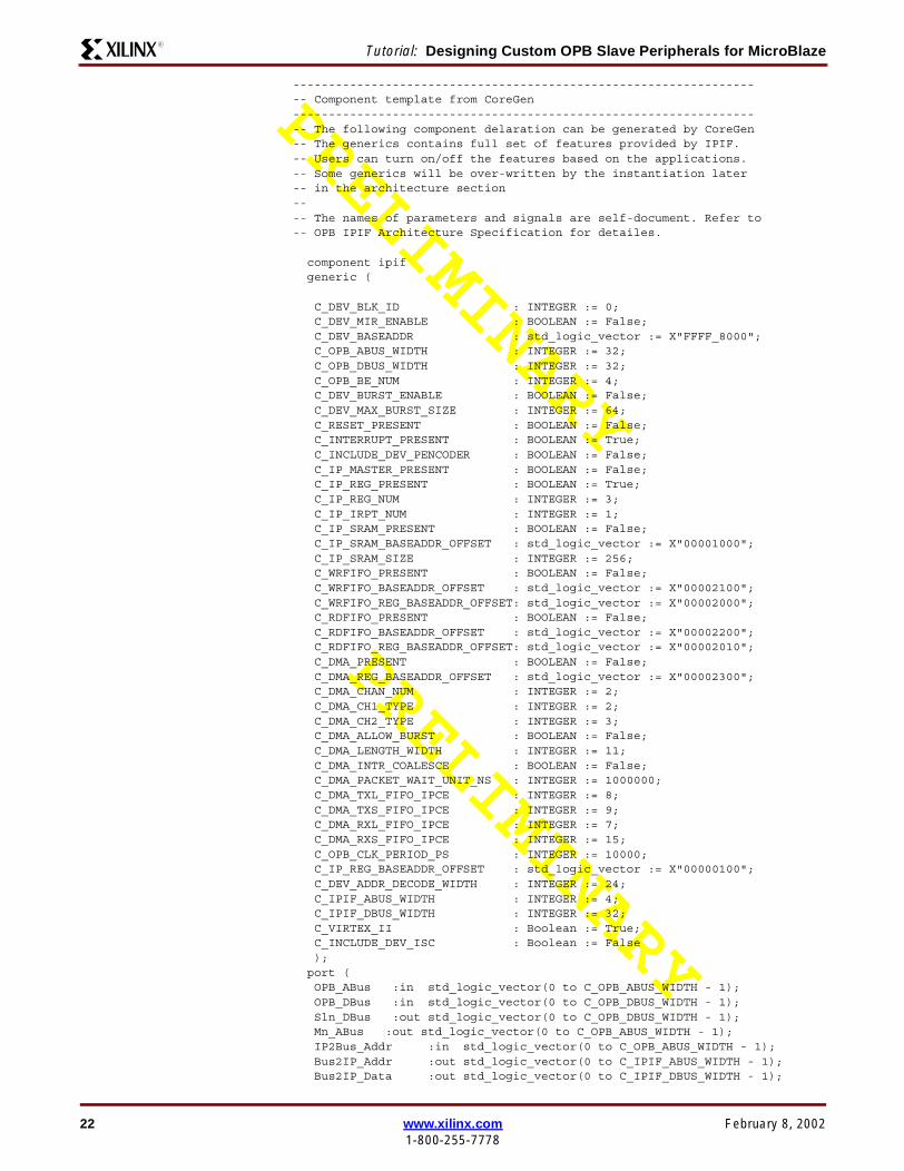
------------------------------------------------------------------- Component template from CoreGen------------------------------------------------------------------- The following component delaration can be generated by CoreGen-- The generics contains full set of features provided by IPIF.-- Users can turn on/off the features based on the applications.-- Some generics will be over-written by the instantiation later-- in the architecture section---- The names of parameters and signals are self-document. Refer to-- OPB IPIF Architecture Specification for detailes.
component ipifgeneric (
C_DEV_BLK_ID : INTEGER := 0;C_DEV_MIR_ENABLE : BOOLEAN := False;C_DEV_BASEADDR : std_logic_vector := X"FFFF_8000";C_OPB_ABUS_WIDTH : INTEGER := 32;C_OPB_DBUS_WIDTH : INTEGER := 32;C_OPB_BE_NUM : INTEGER := 4;C_DEV_BURST_ENABLE : BOOLEAN := False;C_DEV_MAX_BURST_SIZE : INTEGER := 64;C_RESET_PRESENT : BOOLEAN := False;C_INTERRUPT_PRESENT : BOOLEAN := True;C_INCLUDE_DEV_PENCODER : BOOLEAN := False;C_IP_MASTER_PRESENT : BOOLEAN := False;C_IP_REG_PRESENT : BOOLEAN := True;C_IP_REG_NUM : INTEGER := 3;C_IP_IRPT_NUM : INTEGER := 1;C_IP_SRAM_PRESENT : BOOLEAN := False;C_IP_SRAM_BASEADDR_OFFSET : std_logic_vector := X"00001000";C_IP_SRAM_SIZE : INTEGER := 256;C_WRFIFO_PRESENT : BOOLEAN := False;C_WRFIFO_BASEADDR_OFFSET : std_logic_vector := X"00002100";C_WRFIFO_REG_BASEADDR_OFFSET: std_logic_vector := X"00002000";C_RDFIFO_PRESENT : BOOLEAN := False;C_RDFIFO_BASEADDR_OFFSET : std_logic_vector := X"00002200";C_RDFIFO_REG_BASEADDR_OFFSET: std_logic_vector := X"00002010";C_DMA_PRESENT : BOOLEAN := False;C_DMA_REG_BASEADDR_OFFSET : std_logic_vector := X"00002300";C_DMA_CHAN_NUM : INTEGER := 2;C_DMA_CH1_TYPE : INTEGER := 2;C_DMA_CH2_TYPE : INTEGER := 3;C_DMA_ALLOW_BURST : BOOLEAN := False;C_DMA_LENGTH_WIDTH : INTEGER := 11;C_DMA_INTR_COALESCE : BOOLEAN := False;C_DMA_PACKET_WAIT_UNIT_NS : INTEGER := 1000000;C_DMA_TXL_FIFO_IPCE : INTEGER := 8;C_DMA_TXS_FIFO_IPCE : INTEGER := 9;C_DMA_RXL_FIFO_IPCE : INTEGER := 7;C_DMA_RXS_FIFO_IPCE : INTEGER := 15;C_OPB_CLK_PERIOD_PS : INTEGER := 10000;C_IP_REG_BASEADDR_OFFSET : std_logic_vector := X"00000100";C_DEV_ADDR_DECODE_WIDTH : INTEGER := 24;C_IPIF_ABUS_WIDTH : INTEGER := 4;C_IPIF_DBUS_WIDTH : INTEGER := 32;C_VIRTEX_II : Boolean := True;C_INCLUDE_DEV_ISC : Boolean := False);
port (OPB_ABus :in std_logic_vector(0 to C_OPB_ABUS_WIDTH - 1);OPB_DBus :in std_logic_vector(0 to C_OPB_DBUS_WIDTH - 1);Sln_DBus :out std_logic_vector(0 to C_OPB_DBUS_WIDTH - 1);Mn_ABus :out std_logic_vector(0 to C_OPB_ABUS_WIDTH - 1);IP2Bus_Addr :in std_logic_vector(0 to C_OPB_ABUS_WIDTH - 1);Bus2IP_Addr :out std_logic_vector(0 to C_IPIF_ABUS_WIDTH - 1);Bus2IP_Data :out std_logic_vector(0 to C_IPIF_DBUS_WIDTH - 1);

February 8, 2002 www.xilinx.com 231-800-255-7778
Design Practice Using OPB IPIF (Preliminary)R
PRELIMINARY
PRELIMINARY
Bus2IP_Reg_RdCE :out std_logic_vector(0 to C_IP_REG_NUM - 1);Bus2IP_Reg_WrCE :out std_logic_vector(0 to C_IP_REG_NUM - 1);Bus2IP_SRAM_CE :out std_logic;IP2Bus_Data :in std_logic_vector(0 to C_IPIF_DBUS_WIDTH - 1);IP2Bus_WrAck :in std_logic;IP2Bus_RdAck :in std_logic;IP2Bus_Retry :in std_logic;IP2Bus_Error :in std_logic;IP2Bus_ToutSup :in std_logic;IP2DMA_RxLength_Empty : in std_logic;IP2DMA_RxStatus_Empty : in std_logic;IP2DMA_TxLength_Full : in std_logic;IP2DMA_TxStatus_Empty : in std_logic;IP2IP_Addr :in std_logic_vector(0 to C_IPIF_ABUS_WIDTH - 1);IP2RFIFO_Data :in std_logic_vector(0 to 31);IP2RFIFO_WrMark :in std_logic;IP2RFIFO_WrRelease :in std_logic;IP2RFIFO_WrReq :in std_logic;IP2RFIFO_WrRestore :in std_logic;IP2WFIFO_RdMark :in std_logic;IP2WFIFO_RdRelease :in std_logic;IP2WFIFO_RdReq :in std_logic;IP2WFIFO_RdRestore :in std_logic;IP2Bus_MstBE :in std_logic_vector(0 to C_OPB_BE_NUM - 1);IP2Bus_MstWrReq :in std_logic;IP2Bus_MstRdReq :in std_logic;IP2Bus_MstBurst :in std_logic;IP2Bus_MstBusLock :in std_logic;Bus2IP_MstWrAck :out std_logic;Bus2IP_MstRdAck :out std_logic;Bus2IP_MstRetry :out std_logic;Bus2IP_MstError :out std_logic;Bus2IP_MstTimeOut :out std_logic;Bus2IP_MstLastAck :out std_logic;Bus2IP_BE :out std_logic_vector(0 to C_OPB_BE_NUM - 1);Bus2IP_WrReq :out std_logic;Bus2IP_RdReq :out std_logic;Bus2IP_Burst :out std_logic;Mn_request :out std_logic;Mn_busLock :out std_logic;Mn_select :out std_logic;Mn_RNW :out std_logic;Mn_BE :out std_logic_vector(0 to C_OPB_BE_NUM - 1);Mn_seqAddr :out std_logic;OPB_MnGrant :in std_logic;OPB_xferAck :in std_logic;OPB_errAck :in std_logic;OPB_retry :in std_logic;OPB_timeout :in std_logic;Freeze :in std_logic;RFIFO2IP_AlmostFull :out std_logic;RFIFO2IP_Full :out std_logic;RFIFO2IP_Vacancy :out std_logic_vector(0 to 9 );RFIFO2IP_WrAck :out std_logic;OPB_select :in std_logic;OPB_RNW :in std_logic;OPB_seqAddr :in std_logic;OPB_BE :in std_logic_vector(0 to C_OPB_BE_NUM - 1);Sln_xferAck :out std_logic;Sln_errAck :out std_logic;Sln_toutSup :out std_logic;Sln_retry :out std_logic;WFIFO2IP_AlmostEmpty:out std_logic;WFIFO2IP_Data :out std_logic_vector(0 to 31 );WFIFO2IP_Empty :out std_logic;WFIFO2IP_Occupancy :out std_logic_vector(0 to 9 );WFIFO2IP_RdAck :out std_logic;Bus2IP_Clk :out std_logic;

24 www.xilinx.com February 8, 20021-800-255-7778
Tutorial: Designing Custom OPB Slave Peripherals for MicroBlazeR
PRELIMINARY
PRELIMINARY
Bus2IP_DMA_Ack :out std_logic;Bus2IP_Freeze :out std_logic;Bus2IP_Reset :out std_logic;IP2Bus_Clk :in std_logic;IP2Bus_DMA_Req :in std_logic;IP2Bus_IntrEvent :in std_logic_vector(0 to C_IP_IRPT_NUM - 1);IP2INTC_Irpt :out std_logic;OPBClk :in std_logic;Reset :in std_logic
);end component;
...
...
...
begin -- architecture RTL2
----------------------------------------------------------------------------- Instantiate OPB_IPIF to handle OPB interface---------------------------------------------------------------------------
--The following section overwrites default value of generics for--MYGPIO example. Since MYGPIO only needs the "Register" feature,--other IPIF features are set to "False"--*********************************************************--* Because of readability in this document, the following*--* instantiation lists only related signals, it is not a *--* complete source code. *--*********************************************************
u0_ipif: ipifgeneric map (
...
...
C_DEV_BASEADDR => C_BASEADDR, --passed from entityC_OPB_ABUS_WIDTH => C_OPB_AWIDTH,--passed from entityC_OPB_DBUS_WIDTH => C_OPB_DWIDTH,--passed from entityC_DEV_ADDR_DECODE_WIDTH => C_AB, --cal. by function Addr_Bits
C_DEV_BURST_ENABLE => False, --set to false for MYGPIOC_RESET_PRESENT => False, --set to false for MYGPIOC_INTERRUPT_PRESENT => False, --set to false for MYGPIOC_INCLUDE_DEV_PENCODER => False, --set to false for MYGPIOC_IP_MASTER_PRESENT => False, --set to false for MYGPIOC_IP_REG_PRESENT => True, --set to true for MYGPIOC_IP_REG_NUM => 3, --X00/X04/X08 for MYGPIOC_IP_REG_BASEADDR_OFFSET => X"00000000", --X00 for register offsetC_IP_SRAM_PRESENT => False, --set to false for MYGPIOC_WRFIFO_PRESENT => False, --set to false for MYGPIOC_RDFIFO_PRESENT => False, --set to false for MYGPIOC_DMA_PRESENT => False, --set to false for MYGPIO
C_IPIF_ABUS_WIDTH => 4, --not usedC_IPIF_DBUS_WIDTH => 32, --expend 8bit GPIO to 32 to avoid confusionC_INCLUDE_DEV_ISC => False,--set to false for MYGPIO........)
port map (........--Interface to OPB Bus

February 8, 2002 www.xilinx.com 251-800-255-7778
Design Practice Using OPB IPIF (Preliminary)R
PRELIMINARY
PRELIMINARY
Reset => OPB_Rst --I passed from entityOPBClk => OPB_Clk, --I passed from entityOPB_ABus => OPB_ABus, --I passed from entityOPB_DBus => OPB_DBus, --I passed from entityOPB_select => OPB_select, --I passed from entityOPB_RNW => OPB_RNW, --I passed from entityOPB_seqAddr => OPB_seqAddr, --I passed from entityOPB_BE => OPB_BE, --I passed from entitySln_xferAck => GPIO_xferAck, --O passed to entitySln_errAck => GPIO_errAck, --O passed to entitySln_toutSup => GPIO_toutSup, --O passed to entitySln_retry => GPIO_retry, --O passed to entitySln_DBus => GPIO_DBus, --O passed to entity......
--IP Interconnect Interface to MYGPIO registersIP2Bus_Clk => IP2Bus_Clk, --O typically identical to OPB_CLKBus2IP_Reset => Bus2IP_Reset, --O OPB_Rst "ORed" with SW reset.
-- (SW reset is not implemented here)Bus2IP_Addr => open, --O Not ConnectBus2IP_Data => Bus2IP_Data, --OBus2IP_Reg_RdCE => Bus2IP_Reg_RdCE,--OBus2IP_Reg_WrCE => Bus2IP_Reg_WrCE,--OIP2Bus_Data => IP2Bus_Data, --IIP2Bus_WrAck => IP2Bus_WrAck, --IIP2Bus_RdAck => IP2Bus_RdAck, --IIP2Bus_Retry => IP2Bus_Retry, --IIP2Bus_Error => IP2Bus_Error, --IIP2Bus_ToutSup => IP2Bus_ToutSup, --IBus2IP_BE => Bus2IP_BE, --OBus2IP_WrReq => Bus2IP_WrReq, --OBus2IP_RdReq => Bus2IP_RdReq, --O........);
--Unused control signals tie to ground.IP2Bus_retry <= '0';IP2Bus_toutSup <= '0';IP2Bus_Retry <= '0';IP2Bus_Error <= '0';
-----------------------------------------------------Write Access for Memory Mapped Registers in MYGPIO---------------------------------------------------
-- The C program chose to use an integer(32bit) pointer-- to addresses aligned to word boundaries (0,4,8,c..)-- even though MYGPIO is physically 8 bit only.
--Offset 00 GPIO DATA INPUT (READ ONLY)--This register cannot be written by softwareREG_00: process (Bus2IP_Clk, Bus2IP_Reset) isbegin
if Bus2IP_Reset = '1' thengpdata_in <= (others => '0');
elsif Bus2IP_Clk'event and Bus2IP_Clk = '1' thengpdata_in <= GPIO_IO_I; --from external pin
end if;end process REG_00;
--Offset 04 GPIO DATA OUTPUT (R/W) default value 0REG_04: process (Bus2IP_Clk, Bus2IP_Reset) is

26 www.xilinx.com February 8, 20021-800-255-7778
Tutorial: Designing Custom OPB Slave Peripherals for MicroBlazeR
PRELIMINARY
PRELIMINARY
beginif Bus2IP_Reset = '1' then
gpdata_out <= (others => '0');elsif Bus2IP_Clk'event and Bus2IP_Clk = '1' then
if ( Bus2IP_WrReq = '1' and Bus2IP_Reg_WrCE(1) = '1') thengpdata_out <= Bus2IP_Data(24 to 31); -- to external pinend if;
end if;end process REG_04;
--Offset 08 GPIO DATA Tri-State OUTPUT (R/W) default value 1REG_08: process (Bus2IP_Clk, Bus2IP_Reset) isbegin
if Bus2IP_Reset = '1' thengpdata_tri <= (others => '1');
elsif Bus2IP_Clk'event and Bus2IP_Clk = '1' thenif ( Bus2IP_WrReq = '1' and Bus2IP_Reg_WrCE(2) = '1') thengpdata_tri <= Bus2IP_Data(24 to 31); --to external pinend if;
end if;end process REG_08;
--------------------------------Assert WrAck(1-cycle pulse)--after write request------------------------------
--Since WrReq is 1-cycle pulse in this case,--edge detection is not needed
WrAck_PROCESS:process (Bus2IP_Clk,Bus2IP_Reset )begin
if (Bus2IP_Reset = '1') thenIP2Bus_WrAck_i <= '0';
elsif Bus2IP_Clk'event and Bus2IP_Clk = '1' thenIP2Bus_WrAck_i <= Bus2IP_WrReq;
end if;end process;
IP2Bus_WrAck <= IP2Bus_WrAck_i;
-----------------------------------------------------Read Mux for Memory Mapped Registers in MYGPIO---------------------------------------------------
read_process: process (Bus2IP_Clk, Bus2IP_Reset)beginif Bus2IP_Reset = '1' then
read_data <= (others => '0');elsif (Bus2IP_Clk'event and Bus2IP_Clk = '1') then
if (Bus2IP_RdReq = '1') thencase Bus2IP_Reg_RdCE iswhen "100" => read_data <= gpdata_in ;when "010" => read_data <= gpdata_out;when "001" => read_data <= gpdata_tri;when others=> read_data <= (others => '0');end case;end if;
end if;end process;
IP2Bus_Data (24 to 31) <= read_data;IP2Bus_Data (0 to 23 ) <= (others => '0');
--------------------------------Assert RdAck(1-cycle pulse)--after read request

February 8, 2002 www.xilinx.com 271-800-255-7778
Design Practice Using OPB IPIF (Preliminary)R
PRELIMINARY
PRELIMINARY
------------------------------
--Since RdReq is 1-cycle pulse in this case,--edge detection is not needed
RdAck_PROCESS:process (Bus2IP_Clk,Bus2IP_Reset )begin
if (Bus2IP_Reset = '1') thenIP2Bus_RdAck_i <= '0';
elsif Bus2IP_Clk'event and Bus2IP_Clk = '1' thenIP2Bus_RdAck_i <= Bus2IP_RdReq;
end if;end process;
IP2Bus_RdAck <= IP2Bus_RdAck_i;
end architecture RTL2;
Figure 16 and Figure 17 give examples of basic read and write transactions for IPInterconnect. There are separate per-register decodes for the read and write cases, vectorsBus2IP_RegRdCE and Bus2IP_RegWrCE, respectively. Therefore, for the register interface,the Bus2IP_RdReq and Bus2IP_WrReq signals allow the IP to easily generate a one-cycleacknowledgement, IP2Bus_RdAck or IP2Bus_WrAck, by delaying the correspondingrequest signal by the appropriate amount. Refer to OPB IPIF Architecture Specification forother protocol definition.
Figure 15: Implementation Example of MYGPIO Using OPB IPIF
Figure 16: Read Transaction for IP Interconnect Using Register Access Feature
Bus2IP_Clk
Bus2IP_RegRdCE(i)
Bus2IP_RDReq
Valid RD DataIP2Bus_Data
IP2Bus_RdAck
0
xip2055

28 www.xilinx.com February 8, 20021-800-255-7778
Tutorial: Designing Custom OPB Slave Peripherals for MicroBlazeR
PRELIMINARY
PRELIMINARY
Summary of OPB IPIF FeaturesThe above design practice provides an example using the simple register access feature ofOPB IPIF. The full outline of OPB IPIF features is summarized below. Users can refer to theOPB IPIF Architecture Specification for more details, including the functional descriptions,design parameters, interface signals and timing diagrams.
• Synchronous operation• Hardware and optional software reset
• Freeze signal to facilitate debugging• Interrupt Support
• Slave Attachment- Register Interface
- SRAM Interface (for IP with SRAM-like interface)- Support for burst transactions (optional)
• Master Attachment- Support single and burst transactions
- Transaction Qualification interface- Transaction Response interface
• Write FIFO- BRAM based
- Packet support- IP Status flags: Empty, Almost Empty, Occupancy Count
• Read FIFO- BRAM based
- Packet support- IP Status flags: Full, Almost Full, Vacancy Count
• DMA/Scatter Gather- Multiple channels
Figure 17: Write Transaction for IP Interconnect Using Register Access Feature
Bus2IP_Clk
Bus2IP_RegWrCE(i)
Bus2IP_WrReq
Valid WR DataBusIP2_Data
IP2Bus_RdAck
0
xip2056

February 8, 2002 www.xilinx.com 291-800-255-7778
ReferencesR
- Can be used in conjunction with Read and Write FIFOs- Optional packet capability for SG channels
- Optional interrupt coalescing feature for packet SG channels- Uses an IPIF-internal master interface
References• MicroBlaze Software Reference Guide• MicroBlaze Hardware Reference Guide
• OPB IPIF Architecture Specification• IBM On-Chip Peripheral Bus Architecture Specifications v2.1
Revision History
Date Description
September 7, 2001 Initial Release
February 8, 2002 MDK 2.1

30 www.xilinx.com February 8, 20021-800-255-7778
Tutorial: Designing Custom OPB Slave Peripherals for MicroBlazeR