Embed Size (px)
Citation preview

MicroBlaze Micro Controller System v3.0
LogiCORE IP Product Guide
Vivado Design Suite
PG116 April 6, 2016

MicroBlaze MCS v3.0 www.xilinx.com 2PG116 April 6, 2016
Table of ContentsIP Facts
Chapter 1: OverviewFeature Summary. . . . . . . . . . . . . . . . . . . . . . . . . . . . . . . . . . . . . . . . . . . . . . . . . . . . . . . . . . . . . . . . . . 5Licensing and Ordering Information . . . . . . . . . . . . . . . . . . . . . . . . . . . . . . . . . . . . . . . . . . . . . . . . . . . 7
Chapter 2: Product SpecificationStandards . . . . . . . . . . . . . . . . . . . . . . . . . . . . . . . . . . . . . . . . . . . . . . . . . . . . . . . . . . . . . . . . . . . . . . . . 8Performance. . . . . . . . . . . . . . . . . . . . . . . . . . . . . . . . . . . . . . . . . . . . . . . . . . . . . . . . . . . . . . . . . . . . . . 8Resource Utilization. . . . . . . . . . . . . . . . . . . . . . . . . . . . . . . . . . . . . . . . . . . . . . . . . . . . . . . . . . . . . . . . 8Port Descriptions . . . . . . . . . . . . . . . . . . . . . . . . . . . . . . . . . . . . . . . . . . . . . . . . . . . . . . . . . . . . . . . . . . 9Register Space . . . . . . . . . . . . . . . . . . . . . . . . . . . . . . . . . . . . . . . . . . . . . . . . . . . . . . . . . . . . . . . . . . . 10
Chapter 3: Designing with the CoreGeneral Design Guidelines . . . . . . . . . . . . . . . . . . . . . . . . . . . . . . . . . . . . . . . . . . . . . . . . . . . . . . . . . 11Clocking. . . . . . . . . . . . . . . . . . . . . . . . . . . . . . . . . . . . . . . . . . . . . . . . . . . . . . . . . . . . . . . . . . . . . . . . . 11Resets . . . . . . . . . . . . . . . . . . . . . . . . . . . . . . . . . . . . . . . . . . . . . . . . . . . . . . . . . . . . . . . . . . . . . . . . . . 12Protocol Description . . . . . . . . . . . . . . . . . . . . . . . . . . . . . . . . . . . . . . . . . . . . . . . . . . . . . . . . . . . . . . 12
Chapter 4: Design Flow StepsCustomizing and Generating the Core . . . . . . . . . . . . . . . . . . . . . . . . . . . . . . . . . . . . . . . . . . . . . . . . 13Constraining the Core . . . . . . . . . . . . . . . . . . . . . . . . . . . . . . . . . . . . . . . . . . . . . . . . . . . . . . . . . . . . . 34Simulation . . . . . . . . . . . . . . . . . . . . . . . . . . . . . . . . . . . . . . . . . . . . . . . . . . . . . . . . . . . . . . . . . . . . . . 35Synthesis and Implementation . . . . . . . . . . . . . . . . . . . . . . . . . . . . . . . . . . . . . . . . . . . . . . . . . . . . . . 35
Appendix A: Migrating and UpgradingMigrating to the Vivado Design Suite. . . . . . . . . . . . . . . . . . . . . . . . . . . . . . . . . . . . . . . . . . . . . . . . . 36Upgrading in the Vivado Design Suite . . . . . . . . . . . . . . . . . . . . . . . . . . . . . . . . . . . . . . . . . . . . . . . . 36
Appendix B: DebuggingFinding Help on Xilinx.com . . . . . . . . . . . . . . . . . . . . . . . . . . . . . . . . . . . . . . . . . . . . . . . . . . . . . . . . . 38Debug Tools . . . . . . . . . . . . . . . . . . . . . . . . . . . . . . . . . . . . . . . . . . . . . . . . . . . . . . . . . . . . . . . . . . . . . 39Simulation Debug. . . . . . . . . . . . . . . . . . . . . . . . . . . . . . . . . . . . . . . . . . . . . . . . . . . . . . . . . . . . . . . . . 40
Send Feedback

MicroBlaze MCS v3.0 www.xilinx.com 3PG116 April 6, 2016
Hardware Debug . . . . . . . . . . . . . . . . . . . . . . . . . . . . . . . . . . . . . . . . . . . . . . . . . . . . . . . . . . . . . . . . . 40
Appendix C: Application Software DevelopmentXilinx Software Development Kit . . . . . . . . . . . . . . . . . . . . . . . . . . . . . . . . . . . . . . . . . . . . . . . . . . . . 41Device Drivers . . . . . . . . . . . . . . . . . . . . . . . . . . . . . . . . . . . . . . . . . . . . . . . . . . . . . . . . . . . . . . . . . . . 41
Appendix D: Additional Resources and Legal NoticesXilinx Resources . . . . . . . . . . . . . . . . . . . . . . . . . . . . . . . . . . . . . . . . . . . . . . . . . . . . . . . . . . . . . . . . . . 44References . . . . . . . . . . . . . . . . . . . . . . . . . . . . . . . . . . . . . . . . . . . . . . . . . . . . . . . . . . . . . . . . . . . . . . 44Revision History . . . . . . . . . . . . . . . . . . . . . . . . . . . . . . . . . . . . . . . . . . . . . . . . . . . . . . . . . . . . . . . . . . 45Please Read: Important Legal Notices . . . . . . . . . . . . . . . . . . . . . . . . . . . . . . . . . . . . . . . . . . . . . . . . 46
Send Feedback

MicroBlaze MCS v3.0 www.xilinx.com 4PG116 April 6, 2016 Product Specification
IntroductionThe LogiCORE™ IP MicroBlaze™ Micro Controller System (MCS) core is a complete processor system intended for controller applications. It is highly integrated and includes the MicroBlaze processor, local memory for program and data storage as well as a tightly coupled I/O module implementing a standard set of peripherals.
The MicroBlaze processor included in the MicroBlaze MCS core only has two fixed configurations, optimized for minimal area and for high performance. The full-featured MicroBlaze processor is available in the Vivado® Design Suite.
The core uses the Hierarchical IP technology to achieve full integration with the standard Software Development Kit (SDK) flow.
Features• MicroBlaze processor
• Local Memory
• MicroBlaze Debug Module (MDM)
° Debug UART
• Tightly Coupled I/O Module including
° I/O Bus
° Interrupt Controller using fast interrupt mode
° UART
° Fixed Interval Timers
° Programmable Interval Timers
° General Purpose Inputs
° General Purpose Outputs
IP Facts
LogiCORE IP Facts Table
Core Specifics
Supported Device Family(1)
UltraScale+™ FamiliesUltraScale™ Architecture
Zynq®-7000 All Programmable SoC7 Series
Supported User Interfaces
Local Memory Bus (LMB), DynamicReconfiguration Port (DRP)
Resources Performance and Resource Utilization web page
Provided with CoreDesign Files RTL
Example Design Not Provided
Test Bench Not Provided
Constraints File Not Provided
Simulation Model Verilog and/or VHDL Structural
Supported S/W Driver(2) Standalone
Tested Design Flows(3)
Design Entry Vivado Design Suite
Simulation For supported simulators, see theXilinx Design Tools: Release Notes Guide.
Synthesis Vivado Synthesis
SupportProvided by Xilinx at the at the Xilinx Support web page
Notes: 1. For a complete listing of supported devices, see the Vivado IP
catalog.2. Standalone driver details can be found in the SDK directory
(<install_directory>/doc/usenglish/xilinx_drivers.htm). Linux OS and driver support information is available from the Xilinx Wiki page.
3. For the supported versions of the tools, see theXilinx Design Tools: Release Notes Guide.
Send Feedback

MicroBlaze MCS v3.0 www.xilinx.com 5PG116 April 6, 2016
Chapter 1
OverviewThe MicroBlaze™ MCS core is a highly integrated processor system intended for controller applications. Data and program is stored in a local memory, debug is facilitated by the MicroBlaze Debug Module (MDM). A standard set of peripherals is also included, providing basic functionality like interrupt controller, UART, timers and general purpose input and outputs.
Feature SummaryMicroBlazeThe MicroBlaze embedded processor soft core is a reduced instruction set computer (RISC) optimized for implementation in Xilinx® devices. Detailed information on the MicroBlaze processor can be found in the MicroBlaze Processor Reference Guide (UG984) [Ref 1].
The MicroBlaze parameters in the MicroBlaze MCS core are fixed except for the possibility to enable/disable the debug functionality, including debug UART, and the selection of minimum area or high performance. Table 4-2 shows the core parameter values. These values correspond to the MicroBlaze Configuration Wizard Minimum Area configuration,
X-Ref Target - Figure 1-1
Figure 1-1: MicroBlaze Micro Controller System
ILMB
MicroBlaze
LocalMemory Bus
LMB BRAMInterface Controller
Block RAM(Dual Port)
DLMB
LocalMemory Bus
LMB BRAMInterface Controller
I/O Module
MicroBlazeDebug
Optional Feature
Send Feedback

MicroBlaze MCS v3.0 www.xilinx.com 6PG116 April 6, 2016
Chapter 1: Overview
except when the high performance option is selected, in which case a few parameters are changed as listed in the table.
MicroBlaze MCS allows selecting either area or performance optimization. Area optimization uses the MicroBlaze 3-stage pipeline, and does not enable any additional execution units to achieve minimum area. Performance optimization uses the MicroBlaze 5-stage pipeline, and includes a barrel shifter, hardware multiplier, hardware divider, and pattern comparator for higher performance. Unless performance is an issue, it is recommended to use the default area optimization. Choosing performance optimization might also reduce code size, because the additional execution units allow the compiler to generate more efficient code.
Local MemoryLocal memory is used for data and program storage and is implemented using block RAM. The size of the local memory is parameterized and can be between 4 kB and 128 kB. The local memory is connected to MicroBlaze through the Local Memory Bus, LMB, and the LMB BRAM Interface Controller cores. Detailed information on the LMB core can be found in the Local Memory Bus (LMB) V10 Product Guide (PG113) [Ref 2] and detailed information on the LMB BRAM Interface Controller core can be found in the LMB BRAM Interface Controller Product Guide (PG112) [Ref 3].
The memory sizes 4 kB, 8 kB, 16 kB, 32 kB, 64 kB and 128 kB require less resources, and should be used if possible.
The LMB Bus and the LMB BRAM Interface Controller core parameters are fixed except for the memory size and the option to enable Error Correction code (ECC). The parameter values can be found in Tables 4-4 to 4-7.
The local memory provides an option to enable Error Correcting Code (ECC). Error correction corrects single bit errors, and detects double bit errors. Using ECC requires additional block RAM resources to store the check bits, and reduces the number of available memory sizes to 16K, 32K, 48K, 64K, 80K. 96K and 128K. Two additional signals are also added to indicate single bit errors (LMB_CE) and double bit errors (LMB_UE).
DebugThe MDM core connects MicroBlaze debug logic to the Xilinx System Debugger (XSDB). XSDB can be used for downloading software, to set break points, view register and memory contents. If the Debug UART is enabled, XSDB can also be used for standard input and standard output. Detailed information about the MDM core can be found in the MicroBlaze Debug Module (MDM) Product Guide (PG115) [Ref 4].
The MDM parameters, except the JTAG user-defined register and the Debug UART, are fixed and their values can be found in Table 4-8.
Send Feedback

MicroBlaze MCS v3.0 www.xilinx.com 7PG116 April 6, 2016
Chapter 1: Overview
When more than one MicroBlaze MCS core instance with debug enabled is included in the same design, a unique JTAG register must be used for each instance. When a single instance is used, the default value USER2 should be kept unchanged.
I/O ModuleThe I/O Module core is a light-weight implementation of a set of standard I/O functions commonly used in a MicroBlaze processor sub-system. Detailed information about the I/O Module core can be found in the I/O Module Product Guide (PG111) [Ref 5].
The I/O Module core registers are mapped at address 0x80000000, and the I/O Bus is mapped at address 0xC0000000-0xFFFFFFFF in the MicroBlaze memory space. The fixed I/O Module parameter values can be found in Table 4-3.
Licensing and Ordering InformationThis Xilinx LogiCORE™ IP module is provided at no additional cost with the Xilinx Vivado® Design Suite under the terms of the Xilinx End User License. Information about this and other Xilinx LogiCORE IP modules is available at the Xilinx Intellectual Property page. For information about pricing and availability of other Xilinx LogiCORE IP modules and tools, contact your local Xilinx sales representative.
Send Feedback

MicroBlaze MCS v3.0 www.xilinx.com 8PG116 April 6, 2016
Chapter 2
Product Specification
StandardsThe I/O Bus interface provided by the I/O Module core is fully compatible with the Xilinx® Dynamic Reconfiguration Port (DRP). For a detailed description of the DRP, see the 7 Series FPGAs Configuration User Guide (UG470) [Ref 6].
PerformanceThe frequency and latency of the modules in the MicroBlaze™ MCS core are optimized for use together with MicroBlaze. This means that the frequency targets are aligned to MicroBlaze targets as well as the access latency optimized for MicroBlaze data access.
Maximum FrequenciesFor details about maximum frequencies, visit Performance and Resource Utilization.
LatencyData read from I/O Module registers is available two clock cycles after the MicroBlaze load instruction is executed.
Data write to I/O Module registers is performed the clock cycle after the MicroBlaze store instruction is executed. Data accesses to peripherals connected on the I/O bus take three clock cycles plus the number of wait states introduced by the accessed peripheral.
ThroughputThe maximum throughput when using the I/O bus is one read or write access every three clock cycles.
Resource UtilizationFor details about resource utilization, visit Performance and Resource Utilization.
Send Feedback

MicroBlaze MCS v3.0 www.xilinx.com 9PG116 April 6, 2016
Chapter 2: Product Specification
Port DescriptionsThe I/O ports and signals for MicroBlaze MCS core are listed and described in Table 2-1.
Table 2-1: MicroBlaze MCS Signals
Port Name MSB:LSB I/O Description
System SignalsClk I System clock
Reset I System reset
MicroBlaze SignalsTrace_Valid_Instr O Valid instruction on trace port
Trace_Instruction 0:31 O Instruction code
Trace_PC 0:31 O Program counter
Trace_Reg_Write O Instruction writes to the register file
Trace_Reg_Addr 0:4 O Destination register address
Trace_MSR_Reg 0:14 O Machine status register
Trace_New_Reg_Value 0:31 O Destination register update value
Trace_Jump_Taken O Branch instruction evaluated TRUE (taken)
Trace_Delay_Slot O Instruction is in delay slot of a taken branch
Trace_Data_AccessT O Valid D-side memory access
Trace_Data_Address 0:31 O Address for D-side memory access
Trace_Data_Write_Value 0:31 O Value for D-side memory write access
Trace_Data_Byte_Enable 0:3 O Byte enables for D-side memory access
Trace_Data_Read O D-side memory access is a read
Trace_Data_Write O D-side memory access is a write
Local Memory Signals (C_ECC = 1)LMB_CE O Local Memory Correctable Error
LMB_UE O Local Memory Uncorrectable Error
I/O Bus SignalsIO_Addr_Strobe O Address strobe signals valid I/O bus output
signals
IO_Read_Strobe O I/O Bus access is a read
IO_Write_Strobe O I/O Bus access is a write
IO_Address 31:0 O Address for access
IO_Byte_Enable 3:0 O Byte enables for access
IO_Write_Data 31:0 O Data to write for I/O Bus write access
IO_Read_Data 31:0 I Read data for I/O Bus read access
IO_Ready I Ready handshake to end I/O Bus access
Send Feedback

MicroBlaze MCS v3.0 www.xilinx.com 10PG116 April 6, 2016
Chapter 2: Product Specification
Register SpaceThe address map for the MicroBlaze MCS core is shown in Table 2-2.
UART SignalsUART_rxd I Receive Data
UART_txd O Transmit Data
UART_Interrupt O UART Interrupt
FIT SignalsFITx_Interrupt(1) O FITx timer lapsed
FITx_Toggle(1) O Inverted FITx_Toggle when FITx timer lapses
PIT Signals
PITx_Enable(1) I PITx count enable when C_PITx_PRESCALER = External
PITx_Interrupt(1) O PITx timer lapsed
PITx_Toggle(1) O Inverted PITx_Toggle when PITx lapses
GPO SignalsGPIOx_tri_o(1) [C_GPOx_SIZE - 1]:0 O GPOx Output
GPI SignalsGPIOx_tri_i(1) [C_GPIx_SIZE - 1]:0 I GPIx Input
GPIx_Interrupt(1) O GPIx input changed
INTC SignalsINTC_Interrupt(2) 0:[C_INTC_INTR_SIZE - 1] I External interrupt inputs
Notes: 1. x = 1, 2, 3 or 42. Each of the interrupt inputs is treated as synchronous to the clock unless the corresponding bit in the parameter
C_INTC_ASYNC_INTR is set. In that case, the input is synchronized with the number of flip-flops defined by the parameter C_INTC_NUM_SYNC_FF.
Table 2-2: MicroBlaze MCS Address Map
Address (hex) Name Access Type Description0x0 - C_MEMSIZE-1 Local Memory RW Local Memory for MicroBlaze software
C_MEMSIZE - 0x7FFFFFFF Reserved
0x80000000 - 0x800000FF I/O Module RW Mapped to I/O Module registers
0x80000100 - 0xBFFFFFFF Reserved
0xC0000000 - 0xFFFFFFFF I/O Bus RW Mapped to I/O Bus address output
Table 2-1: MicroBlaze MCS Signals (Cont’d)
Port Name MSB:LSB I/O Description
Send Feedback

MicroBlaze MCS v3.0 www.xilinx.com 11PG116 April 6, 2016
Chapter 3
Designing with the CoreThis chapter includes guidelines and additional information to facilitate designing with the core.
General Design Guidelines
I/O Module InterfacesSee the I/O Module Product Guide (PG111) [Ref 5] for design guidelines for the I/O Bus, UART, Fixed Interval Timer, Programmable Interval Timer, General Purpose Output, General Purpose Input, and Interrupt Controller. All of these interfaces are directly connected to the I/O Module inside the MicroBlaze™ MCS core.
MicroBlaze Trace SignalsSee the MicroBlaze Processor Reference Guide (UG081) [Ref 1] for a detailed description of the MicroBlaze Trace signals. The Trace signals are directly connected to the MicroBlaze™ processor inside the MicroBlaze MCS core.
MicroBlaze Debug ModuleSee the Xilinx SDK Help [Ref 7] and the MicroBlaze Debug Module (MDM) Product Guide (PG115) [Ref 4] for a description of debugging with the MicroBlaze Debug Module (MDM) core.
ClockingThe MicroBlaze MCS core is fully synchronous with all clocked elements clocked with the Clk input.
Send Feedback

MicroBlaze MCS v3.0 www.xilinx.com 12PG116 April 6, 2016
Chapter 3: Designing with the Core
ResetsThe Reset input is the master reset input signal for the entire MicroBlaze MCS core. In addition, the entire MicroBlaze MCS core or only the MicroBlaze processor can be reset from XSDB, provided that debug is enabled.
MicroBlaze MCS uses an embedded Processor System Reset IP core to generate internal reset signals. See the Processor System Reset Module Product Guide (PG164) [Ref 14] for a detailed description.
The Reset input is treated as asynchronous, which results in a 10 clock cycle delay until the MicroBlaze processor is reset after the input is set to 1. It is important to ensure that the clock is toggling nominally during this delay, otherwise the processor execution might be incorrect and result in corruption of the local memory.
After the Reset input is cleared to 0, there is a 73 clock cycle delay until the MicroBlaze processor fetches the first instruction of the reset vector at address 0x00000000 in the local memory.
Protocol DescriptionSee the I/O bus timing diagrams in the I/O Module Product Guide (PG111) [Ref 5].
Send Feedback

MicroBlaze MCS v3.0 www.xilinx.com 13PG116 April 6, 2016
Chapter 4
Design Flow StepsThis chapter describes customizing and generating the core, constraining the core, and the simulation, synthesis and implementation steps that are specific to this IP core. More detailed information about the standard Vivado® design flows and the IP integrator can be found in the following Vivado Design Suite user guides:
• Vivado Design Suite User Guide: Designing IP Subsystems using IP Integrator (UG994) [Ref 8]
• Vivado Design Suite User Guide: Designing with IP (UG896) [Ref 9]
• Vivado Design Suite User Guide: Getting Started (UG910) [Ref 10]
• Vivado Design Suite User Guide: Logic Simulation (UG900) [Ref 11]
Customizing and Generating the CoreThis chapter includes information on using Xilinx tools to customize and generate the core using the Vivado Design Suite.
If you are customizing and generating the core in the Vivado IP integrator, see the Vivado Design Suite User Guide: Designing IP Subsystems using IP Integrator (UG994) [Ref 8] for detailed information. IP integrator might auto-compute certain configuration values when validating or generating the design. To check whether the values do change, see the description of the parameter in this chapter. To view the parameter value you can run the validate_bd_design command in the Tcl console.
You can customize the IP for use in your design by specifying values for the various parameters associated with the IP core using the following steps:
1. Select the IP from the IP catalog.
2. Double-click the selected IP or select the Customize IP command from the toolbar or right-click menu.
For details, see the Vivado Design Suite User Guide: Designing with IP (UG896) [Ref 9] and the Vivado Design Suite User Guide: Getting Started (UG910) [Ref 10].
Note: Figures in this chapter are illustrations of the MicroBlaze™ MCS core interface in the Vivado Integrated Design Environment (IDE). This layout might vary from the current version.
Send Feedback

MicroBlaze MCS v3.0 www.xilinx.com 14PG116 April 6, 2016
Chapter 4: Design Flow Steps
The MicroBlaze MCS core parameters are divided into eight tabs: Board, MCS, UART, FIT, PIT, GPO, GPI and Interrupts.
The Board tab is shown in Figure 4-1.
TIP: The board tab is only visible when a board has been defined for the project being used.
Generate Board Based IO Constraints - Enable board specific GPI, GPO, Reset, and UART interfaces. Board constraints are automatically generated for the selected interfaces.
Associate IP interface … - Table to select board interface for Reset, UART, GPIO1, GPIO2, GPIO3, or GPIO4 interface.
X-Ref Target - Figure 4-1
Figure 4-1: Board Tab
Send Feedback

MicroBlaze MCS v3.0 www.xilinx.com 15PG116 April 6, 2016
Chapter 4: Design Flow Steps
The MCS parameter tab is shown in Figure 4-2.
• Memory Size—Defines the local memory size, used to store the MicroBlaze processor software program instructions and data. Increase this value if the software program does not fit in available memory.
• Error Correction Code—Enables Error Correction Codes (ECC) on the local memory to correct single bit errors and detect double bit errors.
• Select MicroBlaze Optimization—Defines MicroBlaze optimization. When set to AREA, the smallest possible processor is implemented, using a 3-stage pipeline without any additional execution units. When set to PERFORMANCE, a higher performance processor is implemented, using a 5-stage pipeline including a barrel shifter, multiplier, divider, and pattern comparator.
• Enable I/O Bus—Enables I/O Bus port.
• Enable MicroBlaze Trace Bus—This option enables the MicroBlaze Trace bus, which provides access to several internal processor signals for trace purposes.
• Enable Debug Support—When debug support is enabled (DEBUG ONLY or DEBUG & UART), it is possible to debug the software using JTAG, from the Xilinx Software
X-Ref Target - Figure 4-2
Figure 4-2: MCS Parameter Tab
Send Feedback

MicroBlaze MCS v3.0 www.xilinx.com 16PG116 April 6, 2016
Chapter 4: Design Flow Steps
Development Kit (SDK) or directly using XSDB. When Debug UART is enabled (DEBUG & UART) it is also possible to use XSDB for software program standard input and standard output.
• Debug JTAG User-defined Register—Specifies the JTAG user-defined register for debug. When more than one MicroBlaze MCS instance with debug enabled is included in the same design, a unique JTAG register must be used for each instance. When a single instance is used, the default value USER2 should be kept unchanged.
The UART parameter tab is shown in Figure 4-3.
• Enable Receiver - Enables UART receiver for character input. This is automatically connected to standard input (stdin) in the software program.
• Enable Transmitter - Enables UART transmitter for character output. This is automatically connected to standard output (stdout) in the software program.
X-Ref Target - Figure 4-3
Figure 4-3: UART Parameter Tab
Send Feedback

MicroBlaze MCS v3.0 www.xilinx.com 17PG116 April 6, 2016
Chapter 4: Design Flow Steps
• Define Baud Rate - Sets the UART baud rate. To get the correct baud rate, the input clock frequency must also be correctly defined.
• Programmable Baud Rate - Determines if the UART baud rate is programmable. The default baud rate is calculated based on the input clock frequency and the defined baud rate.
• Number of Data Bits - Defines the number of data bits used by the UART. Should almost always be set to 8.
• Use Parity - Enable this parameter to use parity checking of the UART characters.
• Even or Odd Parity - Select odd or even parity. Only available when parity is used.
• Implement Receive Interrupt - Generate an interrupt when the UART has received a character. When the interrupt is not enabled the UART must be polled to check if data has been received.
• Implement Transmit Interrupt - Generate an interrupt when the UART has sent a character. When the interrupt is not enabled the UART must be polled to wait until data has been transmitted.
• Implement Error Interrupt - Generate an interrupt if an error occurs when the UART receives a character. This error can be a framing error, an overrun error or a parity error (if parity is used), When the interrupt is not enabled the UART must be polled to check if an error has occurred after a character has been received.
Send Feedback
MicroBlaze MCS v3.0 www.xilinx.com 18PG116 April 6, 2016
Chapter 4: Design Flow Steps
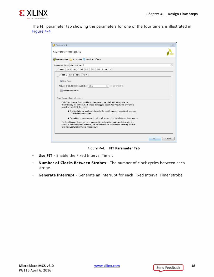
The FIT parameter tab showing the parameters for one of the four timers is illustrated in Figure 4-4.
• Use FIT - Enable the Fixed Interval Timer.
• Number of Clocks Between Strobes - The number of clock cycles between each strobe.
• Generate Interrupt - Generate an interrupt for each Fixed Interval Timer strobe.
X-Ref Target - Figure 4-4
Figure 4-4: FIT Parameter Tab
Send Feedback
MicroBlaze MCS v3.0 www.xilinx.com 19PG116 April 6, 2016
Chapter 4: Design Flow Steps
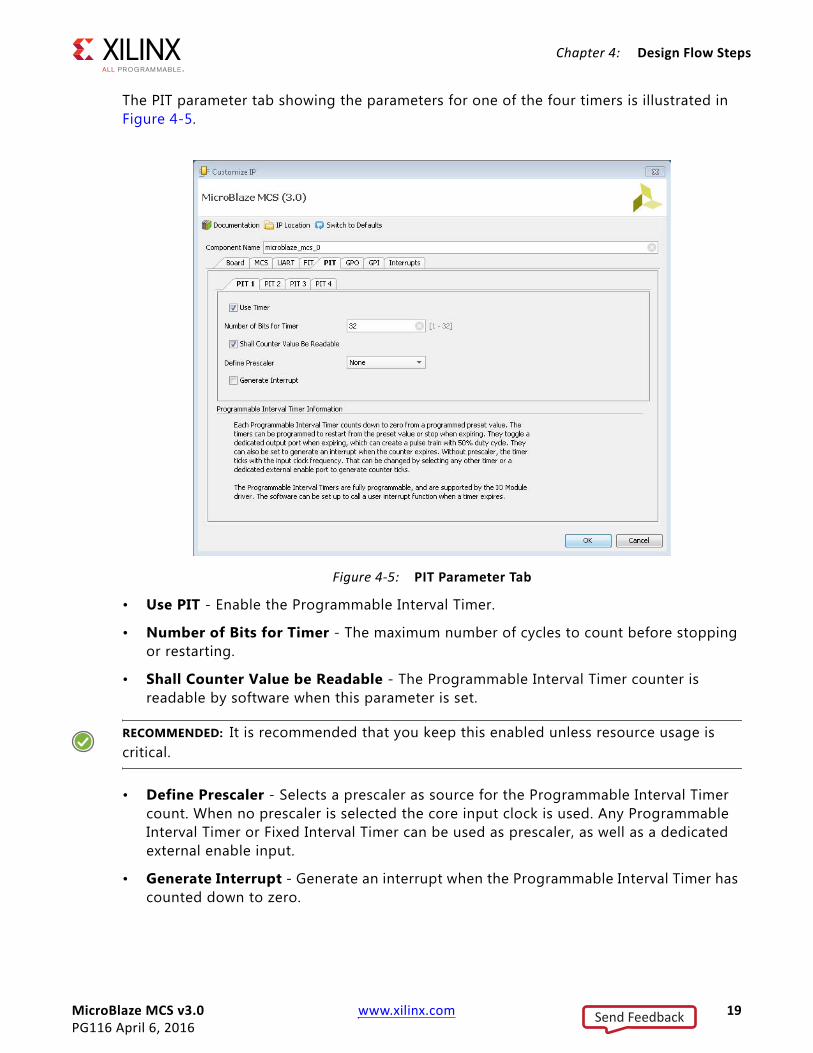
The PIT parameter tab showing the parameters for one of the four timers is illustrated in Figure 4-5.
• Use PIT - Enable the Programmable Interval Timer.
• Number of Bits for Timer - The maximum number of cycles to count before stopping or restarting.
• Shall Counter Value be Readable - The Programmable Interval Timer counter is readable by software when this parameter is set.
RECOMMENDED: It is recommended that you keep this enabled unless resource usage is critical.
• Define Prescaler - Selects a prescaler as source for the Programmable Interval Timer count. When no prescaler is selected the core input clock is used. Any Programmable Interval Timer or Fixed Interval Timer can be used as prescaler, as well as a dedicated external enable input.
• Generate Interrupt - Generate an interrupt when the Programmable Interval Timer has counted down to zero.
X-Ref Target - Figure 4-5
Figure 4-5: PIT Parameter Tab
Send Feedback

MicroBlaze MCS v3.0 www.xilinx.com 20PG116 April 6, 2016
Chapter 4: Design Flow Steps
The GPO parameter tab showing the parameters for the four General Purpose Output ports is illustrated in Figure 4-6.
• Use GPO - Enable the General Purpose Output port.
• Number of Bits - Set the number of bits of the General Purpose Output port.
• Initial Value of GPO - Set the initial value of the General Purpose Output port. The right most bit in the value is assigned to bit 0 of the port, the next right most to bit 1, and so on.
X-Ref Target - Figure 4-6
Figure 4-6: GPO Parameter Tab
Send Feedback

MicroBlaze MCS v3.0 www.xilinx.com 21PG116 April 6, 2016
Chapter 4: Design Flow Steps
The GPI parameter tab showing the parameters for the four General Purpose Input ports is illustrated in Figure 4-7.
• Use GPI - Enable the General Purpose Input port.
• Number of Bits - Set the number of bits of the General Purpose Input port.
• Generate Interrupt - Generate an interrupt when a General Purpose Input changes in the specified way - either any change (Both Edges), only when changed from 0 to 1 (Rising Edge), or only when changed from 1 to 0 (Falling Edge).
X-Ref Target - Figure 4-7
Figure 4-7: GPI Parameter Tab
Send Feedback

MicroBlaze MCS v3.0 www.xilinx.com 22PG116 April 6, 2016
Chapter 4: Design Flow Steps
The Interrupts parameter tab is shown in Figure 4-8.
• Use External Interrupts - Enable the use of external interrupt inputs.
• Number of External Inputs - Select the number of used external interrupt inputs.
• Level or Edge of External Interrupts - Select whether the input is considered level sensitive or edge triggered. Each bit in the value corresponds to the equivalent interrupt input. When a bit is set to one, the interrupt is edge triggered, otherwise it is level sensitive.
• Positive or Negative External Interrupts - Select whether to use High or Low level for level sensitive interrupts, and rising or falling edge for edge triggered interrupts. Each bit in the value corresponds to the equivalent interrupt input When a bit is set to one, High level or rising edge is used, otherwise Low level or falling edge is used.
• Use Low-latency Interrupt Handling - Enable the use of low-latency interrupt handling.
• Interrupts Asynchronous - Set whether to treat interrupts as asynchronous, by adding synchronization flip-flops on the input. Each bit in the value corresponds to the equivalent interrupt input When a bit is set to one, the input is treated as asynchronous.
X-Ref Target - Figure 4-8
Figure 4-8: Interrupts Parameter Tab
Send Feedback

MicroBlaze MCS v3.0 www.xilinx.com 23PG116 April 6, 2016
Chapter 4: Design Flow Steps
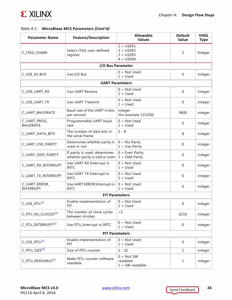
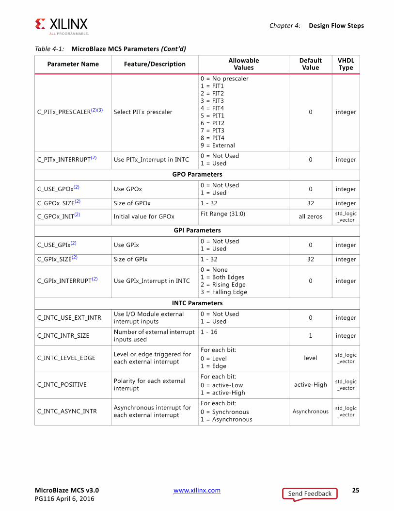
Parameter ValuesTo create a MicroBlaze MCS core that is uniquely tailored for a specific system, certain features can be parameterized. This makes it possible for you to configure a component that only uses the resources required by the system, and operates with the best possible performance. The features that can be parameterized in the MicroBlaze MCS core are shown in Table 4-1.
The internal modules of the MicroBlaze MCS core have fixed configurations detailed in:
• Table 4-2 - MicroBlaze
• Table 4-3 - I/O Module
• Table 4-4 and Table 4-5 - LMB v10
• Table 4-6 and Table 4-7 - LMB BRAM IF Controller
• Table 4-8 - MicroBlaze Debug Module
Table 4-1: MicroBlaze MCS Parameters
Parameter Name Feature/Description AllowableValues
DefaultValue
VHDLType
MCS ParametersC_FAMILY(1) FPGA architecture Supported architectures kintex7 string
C_XDEVICE(1) Device name Supported devices xc7k325t string
C_XPACKAGE(1) FPGA package name Supported packages ffg900 string
C_XSPEEDGRADE(1) FPGA speed grade Supported speed grades -2 string
C_MICROBLAZE_INSTANCE(1) Instance name microblaze_0 string
C_PATH Hierarchical path from top of design to MCS core instance mb/UO
C_FREQ Frequency of CLK input 100000000 integer
C_MEMSIZE Local memory size in bytes
4096 = 4KB8192 = 8KB12288 = 12KB16384 = 16KB20480 = 20KB24576 = 24KB32768 = 32KB36864 = 36KB40960 = 40KB
49152 = 48KB65536 = 64KB69632 = 68KB73728 = 72KB81920 = 80KB98304 = 96KB131072=128KB
8192 Integer
C_DEBUG_ENABLED Enable implementation of debug
0 = NONE1 = DEBUG ONLY2 = DEBUG & UART
0 Integer
C_ECC Enable Error Correcting Code in local memory
0 = Disabled1 = Enabled 0 Integer
C_OPTIMIZATION Select optimization 0 = Area1 = Performance 0 Integer
Send Feedback
MicroBlaze MCS v3.0 www.xilinx.com 24PG116 April 6, 2016
Chapter 4: Design Flow Steps
C_JTAG_CHAIN Select JTAG user-defined register
1 = USER12 = USER23 = USER34 = USER4
2 Integer
I/O Bus Parameter
C_USE_IO_BUS Use I/O Bus 0 = Not Used1 = Used 0 integer
UART Parameters
C_USE_UART_RX Use UART Receive 0 = Not Used1 = Used 0 integer
C_USE_UART_TX Use UART Transmit 0 = Not Used1 = Used 0 integer
C_UART_BAUDRATE Baud rate of the UART in bits per second
integer(for example 115200) 9600 integer
C_UART_PROG_BAUDRATE
Programmable UART baud rate
0 = Not Used1 = Used 0 integer
C_UART_DATA_BITS The number of data bits in the serial frame
5 - 8 8 integer
C_UART_USE_PARITY Determines whether parity is used or not
0 = No Parity1 = Use Parity 0 integer
C_UART_ODD_PARITY If parity is used, determines whether parity is odd or even
0 = Even Parity1 = Odd Parity 0 integer
C_UART_RX_INTERRUPT Use UART RX Interrupt in INTC
0 = Not Used1 = Used 0 integer
C_UART_TX_INTERRUPT Use UART TX Interrupt in INTC
0 = Not Used1 = Used 0 integer
C_UART_ERROR_INTERRUPT
Use UART ERROR Interrupt in INTC
0 = Not Used1 = Used 0 integer
FIT Parameters
C_USE_FITx(1) Enable implementation of FIT
0 = Not Used1 = Used 0 integer
C_FITx_No_CLOCKS(2) The number of clock cycles between strobes
>2 6216 integer
C_FITx_INTERRUPT(2) Use FITx_Interrupt in INTC 0 = Not Used1 = Used 0 integer
PIT Parameters
C_USE_PITx(2) Enable implementation of PIT
0 = Not Used1 = Used 0 integer
C_PITx_SIZE(2) Size of PITx counter 1 - 32 1 integer
C_PITx_READABLE(2) Make PITx counter software readable
0 = Not SWreadable1 = SW readable
1 integer
Table 4-1: MicroBlaze MCS Parameters (Cont’d)
Parameter Name Feature/Description AllowableValues
DefaultValue
VHDLType
Send Feedback
MicroBlaze MCS v3.0 www.xilinx.com 25PG116 April 6, 2016
Chapter 4: Design Flow Steps
C_PITx_PRESCALER(2)(3) Select PITx prescaler
0 = No prescaler1 = FIT12 = FIT23 = FIT34 = FIT45 = PIT16 = PIT27 = PIT38 = PIT49 = External
0 integer
C_PITx_INTERRUPT(2) Use PITx_Interrupt in INTC 0 = Not Used1 = Used 0 integer
GPO Parameters
C_USE_GPOx(2) Use GPOx 0 = Not Used1 = Used 0 integer
C_GPOx_SIZE(2) Size of GPOx 1 - 32 32 integer
C_GPOx_INIT(2) Initial value for GPOx Fit Range (31:0) all zeros std_logic_vector
GPI Parameters
C_USE_GPIx(2) Use GPIx 0 = Not Used1 = Used 0 integer
C_GPIx_SIZE(2) Size of GPIx 1 - 32 32 integer
C_GPIx_INTERRUPT(2) Use GPIx_Interrupt in INTC
0 = None1 = Both Edges2 = Rising Edge3 = Falling Edge
0 integer
INTC Parameters
C_INTC_USE_EXT_INTR Use I/O Module external interrupt inputs
0 = Not Used1 = Used 0 integer
C_INTC_INTR_SIZE Number of external interrupt inputs used
1 - 16 1 integer
C_INTC_LEVEL_EDGE Level or edge triggered for each external interrupt
For each bit:0 = Level1 = Edge
level std_logic_vector
C_INTC_POSITIVE Polarity for each external interrupt
For each bit:0 = active-Low1 = active-High
active-High std_logic_vector
C_INTC_ASYNC_INTR Asynchronous interrupt for each external interrupt
For each bit:0 = Synchronous1 = Asynchronous
Asynchronous std_logic_vector
Table 4-1: MicroBlaze MCS Parameters (Cont’d)
Parameter Name Feature/Description AllowableValues
DefaultValue
VHDLType
Send Feedback

MicroBlaze MCS v3.0 www.xilinx.com 26PG116 April 6, 2016
Chapter 4: Design Flow Steps
C_INTC_NUM_SYNC_FF(1) Number of synchronization flip-flops 0 - 7 2 integer
Notes: 1. Values automatically populated by tool.2. x=1, 2, 3 or 4.3. Selecting PIT prescaler the same as PITx is illegal; for example, PIT2 cannot be prescaler to itself.
Table 4-1: MicroBlaze MCS Parameters (Cont’d)
Parameter Name Feature/Description AllowableValues
DefaultValue
VHDLType
Table 4-2: Internal MicroBlaze Parameters Settings
Parameter Name Feature/Description Value
C_FAMILY Target family Value of MicroBlaze MCSparameter C_FAMILY
C_AREA_OPTIMIZED Select implementation to optimize area with lower instruction throughput
0 when MicroBlaze MCS parameter C_OPTIMIZATION = 11 when MicroBlaze MCS parameter C_OPTIMIZATION = 0
C_INTERCONNECT Select interconnect2= AXI
2
C_ENDIANNESS Select endianness (1 = Little endian) 1
C_FAULT_TOLERANT Implement fault tolerance 0
C_LOCKSTEP_SLAVE Lockstep Slave 0
C_AVOID_PRIMITIVES Disallow FPGA primitives 0
C_PVR Processor version register mode selectionAll other PVR parameters are don’t care.
0
C_RESET_MSR Reset value for MSR register 0x00
C_INSTANCE Instance NameValue of MicroBlaze MCS
parameterC_MICROBLAZE_INSTANCE
C_D_AXI
Data side AXI interface, only used internally to connect to the MDM.All other data side AXI parameters are don’t care.
1 when MicroBlaze MCS parameter
C_DEBUG_ENABLED = 2, 0 otherwise
C_D_LMB Data side LMB interface 1
C_I_AXIInstruction side AXI interface.All other instruction side AXI parameters are don’t care.
0
C_I_LMB Instruction side LMB interface 1
C_USE_BARREL Include barrel shifterValue of MicroBlaze
MCS parameter C_OPTIMIZATION
C_USE_DIV Include hardware dividerValue of MicroBlaze
MCS parameterC_OPTIMIZATION
Send Feedback

MicroBlaze MCS v3.0 www.xilinx.com 27PG116 April 6, 2016
Chapter 4: Design Flow Steps
C_USE_HW_MUL Include hardware multiplierValue of MicroBlaze
MCS parameter C_OPTIMIZATION
C_USE_FPU Include hardware floating point unit 0
C_USE_MSR_INSTR Enable use of instructions: MSRSET and MSRCLR
0
C_USE_PCMP_INSTR Enable use of instructions: CLZ, PCMPBF, PCMPEQ, and PCMPNE
Value of MicroBlaze MCS parameter
C_OPTIMIZATION
C_USE_REORDER_INSTR Enable use of instructions: LBUR, LHUR, LWR, SBR,SHR, SWR, SWAPB, and SWAPH
0
C_*EXCEPTION*(1)
C_OPCODE_0x0_ILLEGALC_USE_STACK_PROTECTION
No exceptions are used0
C_DEBUG_ENABLED MDM Debug interface
1 when MicroBlaze MCS parameter
C_DEBUG_ENABLED > 0, 0 otherwise
C_NUMBER_OF_PC_BRK Number of hardware breakpoints
1 when MicroBlaze MCS parameter
C_DEBUG_ENABLED > 0, 0 otherwise
C_NUMBER_OF_RD_ADDR_BRK Number of read address watchpoints 0
C_NUMBER_OF_WR_ADDR_BRK Number of write address watchpoints 0
C_INTERRUPT_IS_EDGE Level/Edge interrupt 0
C_EDGE_IS_POSITIVE Negative/positive edge interrupt 1
C_FSL_LINKS Number of AXI stream interfaces. All other stream parameters are don’t care
0
C_USE_ICACHE Instruction cache. All other instruction cache parameters are don’t care
0
C_USE_DCACHE Data cache. All other data cache parameters are don’t care
0
C_USE_MMU Memory management. All other MMU parameters are don’t care
0
C_USE_INTERRUPT Enable interrupt handling 2
C_USE_EXT_BRK Enable external break handling
1 when MicroBlaze MCS parameter
C_DEBUG_ENABLED > 0, 0 otherwise
C_USE_EXT_NM_BRK Enable external non-maskable break handling
1 when MicroBlaze MCS parameter
C_DEBUG_ENABLED > 0, 0 otherwise
Table 4-2: Internal MicroBlaze Parameters Settings (Cont’d)
Parameter Name Feature/Description Value
Send Feedback

MicroBlaze MCS v3.0 www.xilinx.com 28PG116 April 6, 2016
Chapter 4: Design Flow Steps
.
C_USE_BRANCH_TARGET_CACHE Enable branch target cache. All other BTC parameters are don’t care
0
Notes: 1. * denotes wildcard and represents any number of characters or numbers.
Table 4-3: Internal I/O Module Parameters Settings
Parameter Name Feature/Description ValueC_BASEADDR LMB I/O Module register base address 0x80000000
C_HIGHADDR LMB I/O Module register high address 0x8000FFFF
C_MASK LMB I/O Module register address space decode mask 0xC0000000
C_IO_HIGHADDR LMB I/O Module I/O bus base address 0xC0000000
C_IO_LOWADDR LMB I/O Module I/O bus address 0xFFFFFFFF
C_IO_MASK LMB I/O Module I/O bus address space decode mask 0xC0000000
C_LMB_AWIDTH LMB address bus width 32
C_LMB_DWIDTH LMB data bus width 32
C_INTC_HAS_FAST Use fast interrupt mode 1
C_INTC_ADDR_WIDTH Interrupt address width 12 - 16(1)
Notes: 1. Value depends on C_MEMSIZE: 12 for 4096, 13 for 8192, 14 for 16384, 15 for 32768, and 16 for 65536.
Table 4-4: Internal LMB_v10 Parameters Settings (ILMB)
Parameter Name Feature/Description Value
C_LMB_NUM_SLAVES Number of LMB slaves 1
C_LMB_AWIDTH LMB address bus width 32
C_LMB_DWIDTH LMB data bus width 32
C_EXT_RESET_HIGH Level of external reset 1 = active-High reset
Table 4-5: Internal LMB_v10 Parameters Settings (DLMB)
Parameter Name Feature/Description Value
C_LMB_NUM_SLAVES Number of LMB slaves 2
C_LMB_AWIDTH LMB address bus width 32
C_LMB_DWIDTH LMB data bus width 32
C_EXT_RESET_HIGH Level of external reset 1 = active-High reset
Table 4-2: Internal MicroBlaze Parameters Settings (Cont’d)
Parameter Name Feature/Description Value
Send Feedback

MicroBlaze MCS v3.0 www.xilinx.com 29PG116 April 6, 2016
Chapter 4: Design Flow Steps
Table 4-6: Internal LMB BRAM IF Controller Parameters Settings (ILMB Controller)
Parameter Name Feature/Description Value
C_BASEADDR LMB BRAM base address 0
C_HIGHADDR LMB BRAM high address Value of MicroBlaze MCS Parameter C_MEMSIZE
C_MASK LMB decode mask 0x80000000
C_LMB_AWIDTH LMB address bus width 32
C_LMB_DWIDTH LMB data bus width 32
C_ECCImplement error correction and detectionAll other ECC as well AXI parameters are don’t care
Value of MicroBlaze MCS parameter C_ECC
Table 4-7: Internal LMB BRAM IF Controller Parameters Settings (DLMB Controller)
Parameter Name Feature/Description Value
C_BASEADDR LMB BRAM base address 0
C_HIGHADDR LMB BRAM high address Value of MicroBlaze MCSParameter C_MEMSIZE
C_MASK LMB decode mask 0x80000000
C_LMB_AWIDTH LMB address bus width 32
C_LMB_DWIDTH LMB data bus width 32
C_ECCImplement error correction and detectionAll other ECC as well as AXI parameters are don’t care
Value of MicroBlaze MCS parameter C_ECC
Table 4-8: MicroBlaze Debug Module Parameters Settings
Parameter Name Feature/Description Value
C_FAMILY FPGA architecture Value of MicroBlaze MCSParameter C_FAMILY
C_MB_DBG_PORTS Number of MicroBlaze debug ports 1
C_USE_UART Enables the UART interface.Set if MicroBlaze MCS
Parameter C_DEBUG_ENABLED=2
C_DBG_MEM_ACCESS Enable AXI memory access from debug 0
C_DBG_REG_ACCESS Enable debug register access from AXI 0
C_USE_CROSS_TRIGGER Enable cross trigger 0
Send Feedback

MicroBlaze MCS v3.0 www.xilinx.com 30PG116 April 6, 2016
Chapter 4: Design Flow Steps
Parameter - Port DependenciesThe width of many of the MicroBlaze MCS signals depends on design parameters. The dependencies between the design parameters and I/O signals are shown in Table 4-9.
Tool FlowThe MicroBlaze MCS core uses the generic tool flow of all Vivado IP catalog cores. The SDK software development flow is briefly described here.
Table 4-9: Parameter-Port Dependencies
Parameter Name Ports (Port width depends on parameter)
C_INTC_INTR_SIZE INTC_Interrupt
C_GPO1_SIZE GPIO1_tri_o
C_GPO2_SIZE GPIO2_tri_o
C_GPO3_SIZE GPIO3_tri_o
C_GPO4_SIZE GPIO4_tri_o
C_GPI1_SIZE GPIO1_tri_i
C_GPI2_SIZE GPIO2_tri_i
C_GPI3_SIZE GPIO3_tri_i
C_GPI4_SIZE GPIO4_tri_i
Send Feedback

MicroBlaze MCS v3.0 www.xilinx.com 31PG116 April 6, 2016
Chapter 4: Design Flow Steps
Generic Vivado Design Suite Tool Flow
The generic tool flow in the Vivado Design Suite is shown in Figure 4-9.
This flow shows the specific steps required to implement a project with the MicroBlaze MCScore in the Vivado Design Suite, and the relationship between the hardware and softwaretools.
• Export Hardware
In the Vivado Design Suite, select File > Export > Export Hardware.
If this is done after generating the bitstream, the bitstream can also be exported by selecting Include bitstream.
X-Ref Target - Figure 4-9
Figure 4-9: Generic Vivado Design Suite Tool Flow
Add IP
ImplementProject
ImportHardware
Description
ImportHardware
CreateSoftware
Software Development KitVivado Design Suite
Implementation
Download and Run
START
SynthesizeProject
GenerateBitstream
Download and Run Software or Debug SoftwareSimulateSoftware
Executable program
HW description HDF file
AssociateELF Files
HW description HDF file
(<toplevel>.hdf)
(<program>.elf)
(<toplevel>.hdf)
Send Feedback

MicroBlaze MCS v3.0 www.xilinx.com 32PG116 April 6, 2016
Chapter 4: Design Flow Steps
• Associate ELF Files
Select Tools > Associate ELF Files.... Initially, the default infinite loop ELF file, mb_bootloop_le.elf, is associated with the MicroBlaze MCS core. ELF files for implementation and simulation are specified separately.
The final bitstream updated with software is typically called <toplevel>.bit, and is normally located in the project directory <project-name>.runs/impl_1. For additional information, see the Vivado Design Suite User Guide: Designing with IP (UG896) [Ref 9].
SDK
The SDK commands to achieve the MicroBlaze MCS specific steps above are as follows:
• Import Hardware Description (All MicroBlaze MCS components are imported with one command)
° Select File > New > Project....
° Expand Xilinx, and select Hardware Platform Specification.
° Click Next.
° Click Browse, and navigate to the hardware description file which is typically called <project-name>.sdk/<toplevel>.hdf.
° Click Finish to perform the import.
After the hardware description has been imported, a standalone board support package can be created, which provides MicroBlaze processor-specific code, and the I/O Module software driver. The MicroBlaze MCS configuration is available in the generated file <processor-name>/include/xparameters.h.
Note: If SDK is started from the Vivado Design Suite using File > Launch SDK this step is performed automatically.
• Import Hardware Implementation
This is done the same way as Import Hardware Description, but using a hardware description file that includes the bitstream.
For additional information, see the Xilinx SDK Help [Ref 7].
Output GenerationFor details, see the Vivado Design Suite User Guide: Designing with IP (UG896) [Ref 9].
Send Feedback

MicroBlaze MCS v3.0 www.xilinx.com 33PG116 April 6, 2016
Chapter 4: Design Flow Steps
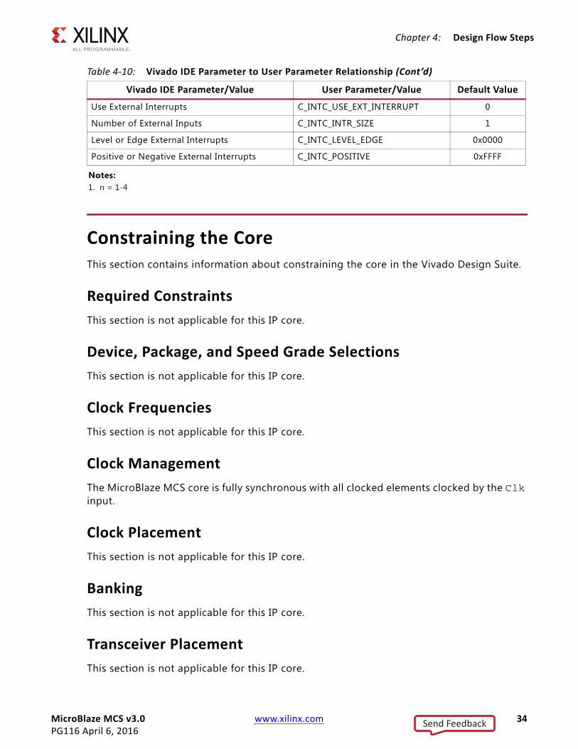
User ParametersTable 4-10 shows the relationship between the fields in the Vivado IDE and the User Parameters (which can be viewed in the Tcl Console).
Table 4-10: Vivado IDE Parameter to User Parameter Relationship
Vivado IDE Parameter/Value User Parameter/Value Default Value
Memory Size C_MEMSIZE 8KB
Error Correction Code C_ECC 0
Select MicroBlaze Optimization C_OPTIMIZATION 0
Enable IO Bus C_USE_IO_BUS 0
Enable MicroBlaze Trace Bus C_TRACE 0
Enable Debug Support C_DEBUG_ENABLED 0
Debug JTAG User-defined Register C_JTAG_CHAIN 2
Enable Receiver C_USE_UART_RX 0
Enable Transmitter C_USE_UART_TX 0
Define Baud Rate C_UART_BAUDRATE 9600
Programmable Baud Rate C_UART_PROG_BAUDRATE 0
Number of Data Bits C_UART_DATA_BITS 8
Use Parity C_UART_USE_PARITY 0
Even or Odd Parity C_UART_ODD_PARITY 0
Implement Receive Interrupt C_UART_RX_INTERRUPT 0
Implement Transmit Interrupt C_UART_TX_INTERRUPT 0
Implement Error Interrupt C_UART_ERROR_INTERRUPT 0
Use FIT C_USE_FITn(1) 0
Number of Clocks Between Strobes C_FITn_No_CLOCKS(1) 6216
Generate Interrupt C_FITn_INTERRUPT(1) 0
Use PIT C_USE_PITn(1) 0
Number of Bits for Timer C_PITn_SIZE(1) 32
Shall Counter Value Be Readable C_PITn_READABLE(1) 1
Define Prescaler C_PITn_PRESCALER(1) 0
Generate Interrupt C_PITn_INTERRUPT(1) 0
Use GPO C_USE_GPOn(1) 0
Number of Bits C_GPOn_SIZE(1) 32
Initial Value of GPO C_GPOn_INIT(1) 0x00000000
Use GPI C_USE_GPIn(1) 0
Number of Bits C_GPIn_SIZE(1) 32
Generate Interrupt C_GPIn_INTERRUPT(1) 0
Send Feedback
MicroBlaze MCS v3.0 www.xilinx.com 34PG116 April 6, 2016
Chapter 4: Design Flow Steps
Constraining the CoreThis section contains information about constraining the core in the Vivado Design Suite.
Required ConstraintsThis section is not applicable for this IP core.
Device, Package, and Speed Grade SelectionsThis section is not applicable for this IP core.
Clock FrequenciesThis section is not applicable for this IP core.
Clock ManagementThe MicroBlaze MCS core is fully synchronous with all clocked elements clocked by the Clk input.
Clock PlacementThis section is not applicable for this IP core.
BankingThis section is not applicable for this IP core.
Transceiver PlacementThis section is not applicable for this IP core.
Use External Interrupts C_INTC_USE_EXT_INTERRUPT 0
Number of External Inputs C_INTC_INTR_SIZE 1
Level or Edge External Interrupts C_INTC_LEVEL_EDGE 0x0000
Positive or Negative External Interrupts C_INTC_POSITIVE 0xFFFF
Notes: 1. n = 1-4
Table 4-10: Vivado IDE Parameter to User Parameter Relationship (Cont’d)
Vivado IDE Parameter/Value User Parameter/Value Default Value
Send Feedback

MicroBlaze MCS v3.0 www.xilinx.com 35PG116 April 6, 2016
Chapter 4: Design Flow Steps
I/O Standard and PlacementThis section is not applicable for this IP core.
SimulationFor comprehensive information about Vivado Design Suite simulation components, as well as information about using supported third party tools, see the Vivado Design Suite User Guide: Logic Simulation (UG900) [Ref 11].
IMPORTANT: For cores targeting 7 series or Zynq®-7000 devices, UNIFAST libraries are not supported. Xilinx IP is tested and qualified with UNISIM libraries only.
Synthesis and ImplementationFor details about synthesis and implementation, see the Vivado Design Suite User Guide: Designing with IP (UG896) [Ref 9].
Send Feedback

MicroBlaze MCS v3.0 www.xilinx.com 36PG116 April 6, 2016
Appendix A
Migrating and UpgradingThis appendix contains information about migrating a design from ISE® to the Vivado® Design Suite, and for upgrading to a more recent version of the IP core. For customers upgrading in the Vivado Design Suite, important details (where applicable) about any port changes and other impact to user logic are included.
Migrating to the Vivado Design SuiteFor information on migrating from Xilinx ISE Design Suite tools to the Vivado Design Suite, see the ISE to Vivado Design Suite Migration Guide (UG911) [Ref 12].
Upgrading in the Vivado Design SuiteThis section provides information about any changes to the user logic or port designations that take place when you upgrade to a more current version of this IP core in the Vivado Design Suite.
The parameters, GPI1_INTERRUPT, GPI2_INTERRUPT, GPI3_INTERRUPT, and GPI4_INTERRUPT were changed in v2.0 of the core released in Vivado 2013.1, to add support for triggering GPI interrupts on either a rising or falling edge.
The parameters, USE_BOARD_FLOW, GPIO1_BOARD_INTERFACE, GPIO1_BOARD_INTERFACE, GPIO1_BOARD_INTERFACE, GPIO1_BOARD_INTERFACE, and UART_BOARD_INTERFACE were added in v2.0 of the core released in 2013.3, to add support for board level constraints.
The port names UART_Rx, UART_Tx, GPOn, and GPIn have been changed to UART_rxd, UART_txd, GPIOn_tri_o and GPIOn_tri_i respectively in v3.0 of the core.
The bus interface name IOBUS has been changed to IO in v3.0 of the core.
The parameters C_OPTIMIZATION and C_ECC were added in v3.0 of the core.
Because hardware export is performed with the generic Vivado tool flow in v3.0 of the core, the processor name is defined by the design hierarchy. This can be seen in the Software Development Kit, and in the Board Support Package generated files, in particular the defines in xparameters.h. The generic hardware export also results in changed memory
Send Feedback

MicroBlaze MCS v3.0 www.xilinx.com 37PG116 April 6, 2016
Appendix A: Migrating and Upgrading
definitions in the automatically generated linker scripts for memory sizes requiring two physical LMB memories (12KB, 20KB, 24KB, 36KB, 40KB, 48KB, 68KB, 72KB, 80KB, 96KB). The two memory blocks can be merged by manually editing the linker script.
Send Feedback

MicroBlaze MCS v3.0 www.xilinx.com 38PG116 April 6, 2016
Appendix B
DebuggingThis appendix includes details about resources available on the Xilinx Support website and debugging tools.
Finding Help on Xilinx.comTo help in the design and debug process when using the MicroBlaze MCS core, the Xilinx Support web page contains key resources such as product documentation, release notes, answer records, information about known issues, and links for obtaining further product support.
DocumentationThis product guide is the main document associated with the MicroBlaze MCS core. This guide, along with documentation related to all products that aid in the design process, can be found on the Xilinx Support web page or by using the Xilinx® Documentation Navigator.
Download the Xilinx Documentation Navigator from the Downloads page. For more information about this tool and the features available, open the online help after installation.
Answer RecordsAnswer Records include information about commonly encountered problems, helpful information on how to resolve these problems, and any known issues with a Xilinx product. Answer Records are created and maintained daily ensuring that users have access to the most accurate information available.
Answer Records for this core can be located by using the Search Support box on the main Xilinx support web page. To maximize your search results, use proper keywords such as
• Product name
• Tool message(s)
• Summary of the issue encountered
A filter search is available after results are returned to further target the results.
Send Feedback

MicroBlaze MCS v3.0 www.xilinx.com 39PG116 April 6, 2016
Appendix B: Debugging
Master Answer Record for the MicroBlaze MCS Core
AR: 54414
Technical SupportXilinx provides technical support at the Xilinx Support web page for this LogiCORE™ IP product when used as described in the product documentation. Xilinx cannot guarantee timing, functionality, or support if you do any of the following:
• Implement the solution in devices that are not defined in the documentation.
• Customize the solution beyond that allowed in the product documentation.
• Change any section of the design labeled DO NOT MODIFY.
To contact Xilinx Technical Support, navigate to the Xilinx Support web page.
Debug ToolsThe main tool available to address MicroBlaze MCS design issues is the Vivado® Design Suite debug feature.
Vivado Design Suite Debug FeatureThe Vivado Design Suite debug feature inserts logic analyzer and virtual I/O cores directly into your design. The debug feature also allows you to set trigger conditions to capture application and integrated block port signals in hardware. Captured signals can then be analyzed. This feature in the Vivado IDE is used for logic debugging and validation of a design running in Xilinx devices.
The Vivado logic analyzer is used with the logic debug IP cores, including:
• ILA 2.0 (and later versions)
• VIO 2.0 (and later versions)
See Vivado Design Suite User Guide: Programming and Debugging (UG908) [Ref 13].
Reference BoardsAll 7 series and UltraScale™ Xilinx development boards support the MicroBlaze MCS core. These boards can be used to prototype designs and establish that the core can communicate with the system.
Send Feedback

MicroBlaze MCS v3.0 www.xilinx.com 40PG116 April 6, 2016
Appendix B: Debugging
Simulation DebugThe simulation debug flow for Mentor Graphics Questa Simulator (QuestaSim) is described below. A similar approach can be used with other simulators.
• Check for the latest supported versions of QuestaSim in the Xilinx Design Tools: Release Notes Guide. Is this version being used? If not, update to this version.
• If using Verilog, do you have a mixed mode simulation license? If not, obtain a mixed-mode license.
• Ensure that the proper libraries are compiled and mapped. In the Vivado Design Suite Flow > Simulation Settings can be used to define the libraries.
• Have you associated the intended software program for the MicroBlaze processor with the simulation? Use the command Tools > Associate ELF Files in the Vivado Design Suite.
Hardware DebugThis section provides debug steps for common issues. The Vivado Design Suite debug feature is a valuable resource to use in hardware debug.
General ChecksEnsure that all the timing constraints for the core were properly incorporated from the example design and that all constraints were met during implementation.
• Does it work in post-place and route timing simulation? If problems are seen in hardware but not in timing simulation, this could indicate a PCB issue. Ensure that all clock sources are active and clean.
• If using MMCMs in the design, ensure that all MMCMs have obtained lock by monitoring the locked port.
Send Feedback

MicroBlaze MCS v3.0 www.xilinx.com 41PG116 April 6, 2016
Appendix C
Application Software Development
Xilinx Software Development KitThe MicroBlaze™ MCS core can be used with the Xilinx® Software Development Kit (SDK), in the same way as any embedded system.
The specific steps needed with the MicroBlaze MCS core are described in SDK in Chapter 4.
Device DriversThe I/O Module is supported by the I/O Module driver (iomodule), included with the Xilinx Software Development Kit. The I/O Module driver API is designed to be as similar as possible to the equivalent discrete peripheral driver API.
The correspondence between the iomodule driver API and the intc, uartlite, tmrctr and gpio driver API is listed in Table C-1. The I/O Module functions are equivalent to the discrete driver counterparts in terms of semantics and syntax, except that all take an XIOModule instance pointer.
Table C-1: I/O Module Driver API Correspondence
I/O Module Function Discrete Function Remark
XIOModule_Initialize XIntc_Initialize Should only be called once for the entire I/O Module driver
XIOModule_Start XIntc_Start
XIOModule_Stop XIntc_Stop
XIOModule_Connect XIntc_Connect
XIOModule_Disconnect XIntc_Disconnect
XIOModule_Enable XIntc_Enable
XIOModule_Disable XIntc_Disable
XIOModule_Acknowledge XIntc_Acknowledge
XIOModule_LookupConfig XIntc_LookupConfig
XIOModule_ConnectFastHandler XIntc_ConnectFastHandler
XIOModule_SetNormalIntrMode XIntc_SetNormalIntrMode
Send Feedback

MicroBlaze MCS v3.0 www.xilinx.com 42PG116 April 6, 2016
Appendix C: Application Software Development
XIOModule_VoidInterruptHandler XIntc_VoidInterruptHandler
XIOModule_InterruptHandler XIntc_InterruptHandler
XIOModule_SetOptions XIntc_SetOptions
XIOModule_GetOptions XIntc_GetOptions
XIOModule_SelfTest XIntc_SelfTest
XIntc_SimulateIntr Corresponding hardware function not available in I/O Module
XIOModule_Initialize XUartLite_Initialize Should only be called once for the entire I/O Module driver
XIOModule_CfgInitialize XUartLite_CfgInitialize Should only be called once for the entire I/O Module driver
XIOModule_ResetFifos XUartLite_ResetFifos
XIOModule_Send XUartLite_Send
XIOModule_Recv XUartLite_Recv
XIOModule_IsSending XUartLite_IsSending
XIOModule_SetBaudRate Programmable baud rate not available in discrete hardware
XIOModule_GetStats XUartLite_GetStats
XIOModule_ClearStats XUartLite_ClearStats
XUartLite_SelfTest The I/O Module self-test uses UART TX for output
XIOModule_Uart_EnableInterrupt XUartLite_EnableInterrupt
XIOModule_Uart_DisableInterrupt XUartLite_DisableInterrupt
XIOModule_SetRecvHandler XUartLite_SetRecvHandler
XIOModule_SetSendHandler XUartLite_SetSendHandler
XIOModule_Uart_InterruptHandler XUartLite_InterruptHandler
XIOModule_Initialize XTmrCtr_Initialize Should only be called once for the entire I/O Module driver
XIOModule_Timer_Start XTmrCtr_Start Added Timer to function name to avoid conflicting names
XIOModule_Timer_Stop XTmrCtr_Stop Added Timer to function name to avoid conflicting names
XIOModule_GetValue XTmrCtr_GetValue
XIOModule_SetResetValue XTmrCtr_SetResetValue
XIOModule_GetCaptureValue XTmrCtr_GetCaptureValue
XIOModule_IsExpired XTmrCtr_IsExpired
XIOModule_Reset XTmrCtr_Reset
XIOModule_Timer_SetOptions XTmrCtr_SetOptions Added Timer to function name to avoid conflicting names
Table C-1: I/O Module Driver API Correspondence (Cont’d)
I/O Module Function Discrete Function Remark
Send Feedback

MicroBlaze MCS v3.0 www.xilinx.com 43PG116 April 6, 2016
Appendix C: Application Software Development
XIOModule_Timer_GetOptions XTmrCtr_GetOptions Added Timer to function name to avoid conflicting names
XIOModule_Timer_GetStats XTmrCtr_GetStats Added Timer to function name to avoid conflicting names
XIOModule_Timer_ClearStats XTmrCtr_ClearStats Added Timer to function name to avoid conflicting names
XIOModule_Timer_SelfTest XTmrCtr_SelfTest Added Timer to function name to avoid conflicting names
XIOModule_SetHandler XTmrCtr_SetHandler
XIOModule_Timer_InterruptHandler XTmrCtr_InterruptHandler Added Timer to function name to avoid conflicting names
XIOModule_Initialize XGpio_Initialize Should only be called once for the entire I/O Module driver
XIOModule_CfgInitialize XGpio_CfgInitialize Should only be called once for the entire I/O Module driver
XGpio_SetDataDirection Separate GPI/GPO, so not necessary
XGpio_GetDataDirection Separate GPI/GPO, so not necessary
XIOModule_DiscreteRead XGpio_DiscreteRead
XIOModule_DiscreteWrite XGpio_DiscreteWrite
XIOModule_DiscreteSet XGpio_DiscreteSet
XIOModule_DiscreteClear XGpio_DiscreteClear
XGpio_SelfTest No self-test of GPI or GPO provided
XGpio_InterruptGlobalEnableCorresponding hardware function not available in I/O Module
XGpio_InterruptGlobalDisableCorresponding hardware function not available in I/O Module
XGpio_InterruptEnableCorresponding hardware function not available in I/O Module
XGpio_InterruptDisableCorresponding hardware function not available in I/O Module
XGpio_InterruptClearCorresponding hardware function not available in I/O Module
XGpio_InterruptGetEnabledCorresponding hardware function not available in I/O Module
XGpio_InterruptGetStatusCorresponding hardware function not available in I/O Module
Table C-1: I/O Module Driver API Correspondence (Cont’d)
I/O Module Function Discrete Function Remark
Send Feedback

MicroBlaze MCS v3.0 www.xilinx.com 44PG116 April 6, 2016
Appendix D
Additional Resources and Legal Notices
Xilinx ResourcesFor support resources such as Answers, Documentation, Downloads, and Forums, see Xilinx Support.
ReferencesThese documents provide supplemental material useful with this user guide:
1. MicroBlaze Processor Reference Guide (UG984)
2. Local Memory Bus (LMB) V10 Product Guide (PG113)
3. IP Processor LMB BRAM Interface Controller Product Guide (PG112)
4. MicroBlaze Debug Module (MDM) Product Guide (PG115)
5. I/O Module Product Guide (PG111)
6. 7 Series FPGAs Configuration User Guide (UG470)
7. Xilinx Software Development Kit Help (UG782)
8. Vivado® Design Suite User Guide: Designing IP Subsystems using IP Integrator (UG994)
9. Vivado Design Suite User Guide: Designing with IP (UG896)
10. Vivado Design Suite User Guide: Getting Started (UG910)
11. Vivado Design Suite User Guide - Logic Simulation (UG900)
12. ISE® to Vivado Design Suite Migration Guide (UG911)
13. Vivado Design Suite User Guide: Programming and Debugging (UG908)
14. Processor System Reset Module LogiCORE IP Product Guide (PG164)
Send Feedback

MicroBlaze MCS v3.0 www.xilinx.com 45PG116 April 6, 2016
Appendix D: Additional Resources and Legal Notices
Revision HistoryThe following table shows the revision history for this document.
Date Version Revision
04/06/2016 3.0 • Added support for Hierarchical IP technology.• Added option to enable Error Correction Codes (ECC) on the internal block
RAM.• Added option to set MicroBlaze optimization (area or performance).
11/18/2015 2.3 Added support for UltraScale+ families.
06/24/2015 2.3 Moved performance and resource utilization data to the web.
04/01/2015 2.3 Updated due to core revision.
04/02/2014 2.2 • Updated due to core revision.• Option to enable Debug UART added.• Additional memory sizes added.
12/18/2013 2.1 • Updated due to core revision.• Synchronization flip-flops added on asynchronous interrupt inputs.
10/02/2013 2.0 • Document version number advanced to match the core version number.• Updated due to core revision.• Added description of board interfaces.
03/20/2013 1.0 Initial release as a Product Guide; replaces PG048. No other documentation changes.
Send Feedback

MicroBlaze MCS v3.0 www.xilinx.com 46PG116 April 6, 2016
Appendix D: Additional Resources and Legal Notices
Please Read: Important Legal NoticesThe information disclosed to you hereunder (the “Materials”) is provided solely for the selection and use of Xilinx products. To the maximum extent permitted by applicable law: (1) Materials are made available "AS IS" and with all faults, Xilinx hereby DISCLAIMS ALL WARRANTIES AND CONDITIONS, EXPRESS, IMPLIED, OR STATUTORY, INCLUDING BUT NOT LIMITED TO WARRANTIES OF MERCHANTABILITY, NON-INFRINGEMENT, OR FITNESS FOR ANY PARTICULAR PURPOSE; and (2) Xilinx shall not be liable (whether in contract or tort, including negligence, or under any other theory of liability) for any loss or damage of any kind or nature related to, arising under, or in connection with, the Materials (including your use of the Materials), including for any direct, indirect, special, incidental, or consequential loss or damage (including loss of data, profits, goodwill, or any type of loss or damage suffered as a result of any action brought by a third party) even if such damage or loss was reasonably foreseeable or Xilinx had been advised of the possibility of the same. Xilinx assumes no obligation to correct any errors contained in the Materials or to notify you of updates to the Materials or to product specifications. You may not reproduce, modify, distribute, or publicly display the Materials without prior written consent. Certain products are subject to the terms and conditions of Xilinx’s limited warranty, please refer to Xilinx’s Terms of Sale which can be viewed at http://www.xilinx.com/legal.htm#tos; IP cores may be subject to warranty and support terms contained in a license issued to you by Xilinx. Xilinx products are not designed or intended to be fail-safe or for use in any application requiring fail-safe performance; you assume sole risk and liability for use of Xilinx products in such critical applications, please refer to Xilinx’s Terms of Sale which can be viewed at http://www.xilinx.com/legal.htm#tos.Automotive Applications DisclaimerXILINX PRODUCTS ARE NOT DESIGNED OR INTENDED TO BE FAIL-SAFE, OR FOR USE IN ANY APPLICATION REQUIRING FAIL-SAFE PERFORMANCE, SUCH AS APPLICATIONS RELATED TO: (I) THE DEPLOYMENT OF AIRBAGS, (II) CONTROL OF A VEHICLE, UNLESS THERE IS A FAIL-SAFE OR REDUNDANCY FEATURE (WHICH DOES NOT INCLUDE USE OF SOFTWARE IN THE XILINX DEVICE TO IMPLEMENT THE REDUNDANCY) AND A WARNING SIGNAL UPON FAILURE TO THE OPERATOR, OR (III) USES THAT COULD LEAD TO DEATH OR PERSONAL INJURY. CUSTOMER ASSUMES THE SOLE RISK AND LIABILITY OF ANY USE OF XILINX PRODUCTS IN SUCH APPLICATIONS.© Copyright 2013–2016 Xilinx, Inc. Xilinx, the Xilinx logo, Artix, ISE, Kintex, Spartan, Virtex, Vivado, Zynq, and other designated brands included herein are trademarks of Xilinx in the United States and other countries. AMBA, AMBA Designer, ARM, ARM1176JZ-S, CoreSight, Cortex, and PrimeCell are trademarks of ARM in the EU and other countries. All other trademarks are the property of their respective owners.
Send Feedback