Embed Size (px)
Citation preview

AXI Interface Based KC705 Embedded Kit MicroBlaze Processor Subsystem Hardware Tutorial (ISE Design Suite 14.5)
UG914 (v2.0) April 23, 2013

KC705 MicroBlaze Processor Subsystem Tutorial www.xilinx.com UG914 (v2.0) April 23, 2013
Notice of DisclaimerThe information disclosed to you hereunder (the “Materials”) is provided solely for the selection and use of Xilinx products. To the maximum extent permitted by applicable law: (1) Materials are made available “AS IS” and with all faults, Xilinx hereby DISCLAIMS ALL WARRANTIES AND CONDITIONS, EXPRESS, IMPLIED, OR STATUTORY, INCLUDING BUT NOT LIMITED TO WARRANTIES OF MERCHANTABILITY, NON-INFRINGEMENT, OR FITNESS FOR ANY PARTICULAR PURPOSE; and (2) Xilinx shall not be liable (whether in contract or tort, including negligence, or under any other theory of liability) for any loss or damage of any kind or nature related to, arising under, or in connection with, the Materials (including your use of the Materials), including for any direct, indirect, special, incidental, or consequential loss or damage (including loss of data, profits, goodwill, or any type of loss or damage suffered as a result of any action brought by a third party) even if such damage or loss was reasonably foreseeable or Xilinx had been advised of the possibility of the same. Xilinx assumes no obligation to correct any errors contained in the Materials or to notify you of updates to the Materials or to product specifications. You may not reproduce, modify, distribute, or publicly display the Materials without prior written consent. Certain products are subject to the terms and conditions of the Limited Warranties which can be viewed at http://www.xilinx.com/warranty.htm; IP cores may be subject to warranty and support terms contained in a license issued to you by Xilinx. Xilinx products are not designed or intended to be fail-safe or for use in any application requiring fail-safe performance; you assume sole risk and liability for use of Xilinx products in Critical Applications: http://www.xilinx.com/warranty.htm#critapps.
Automotive Applications DisclaimerXILINX PRODUCTS ARE NOT DESIGNED OR INTENDED TO BE FAIL-SAFE, OR FOR USE IN ANY APPLICATION REQUIRING FAIL-SAFE PERFORMANCE, SUCH AS APPLICATIONS RELATED TO: (I) THE DEPLOYMENT OF AIRBAGS, (II) CONTROL OF A VEHICLE, UNLESS THERE IS A FAIL-SAFE OR REDUNDANCY FEATURE (WHICH DOES NOT INCLUDE USE OF SOFTWARE IN THE XILINX DEVICE TO IMPLEMENT THE REDUNDANCY) AND A WARNING SIGNAL UPON FAILURE TO THE OPERATOR, OR (III) USES THAT COULD LEAD TO DEATH OR PERSONAL INJURY. CUSTOMER ASSUMES THE SOLE RISK AND LIABILITY OF ANY USE OF XILINX PRODUCTS IN SUCH APPLICATIONS.
© Copyright 2012–2013 Xilinx, Inc. Xilinx, the Xilinx logo, Artix, ISE, Kintex, Spartan, Vivado, Virtex, Zynq, and other designated brands included herein are trademarks of Xilinx in the United States and other countries. All other trademarks are the property of their respective owners.
Revision HistoryThe following table shows the revision history for this document.
Date Version Revision
09/04/2012 1.0 Initial Xilinx Release.
11/05/2012 1.1 Changed “system_top - STRUCTURE” to “Design Sources and system_top -STRUCTURE” under Create the Hardware Platform and Customize the Embedded Hardware Platform. Updated Figure 1-12, Figure 1-21, and Figure 1-22. Added step a under Export the BIST Hardware Platform to SDK. Changed “enter the new connection name” to “select from the drop down menu” in step 6 under Connect the Ports.
04/23/2013 2.0 Updated for ISE® Design Suite 14.5. Changed board_test_app_console.elf to board_test_app_Console.elf in step 9 under Executing the System, page 9. Under Connect the Ports, page 27, step 6 changed. Replaced Figure 1-5, Figure 1-6, Figure 1-7, Figure 1-10, Figure 1-12, Figure 1-14, Figure 1-15, Figure 1-17, Figure 1-18, Figure 1-19, Figure 1-20, Figure 1-21, and Figure 1-22. Enhanced Appendix A, Additional Resources.
KC705 MicroBlaze Processor Subsystem Tutorial www.xilinx.com 3UG914 (v2.0) April 23, 2013
Revision History . . . . . . . . . . . . . . . . . . . . . . . . . . . . . . . . . . . . . . . . . . . . . . . . . . . . . . . . . . . . . 2
Chapter 1: KC705 Embedded Kit MicroBlaze Processor Subsystem Hardware Tutorial
Introduction . . . . . . . . . . . . . . . . . . . . . . . . . . . . . . . . . . . . . . . . . . . . . . . . . . . . . . . . . . . . . . . . . 5Hardware and Software Requirements . . . . . . . . . . . . . . . . . . . . . . . . . . . . . . . . . . . . . . . 5Prerequisites . . . . . . . . . . . . . . . . . . . . . . . . . . . . . . . . . . . . . . . . . . . . . . . . . . . . . . . . . . . . . . . . . 6System Overview . . . . . . . . . . . . . . . . . . . . . . . . . . . . . . . . . . . . . . . . . . . . . . . . . . . . . . . . . . . . 6Included Files and Systems. . . . . . . . . . . . . . . . . . . . . . . . . . . . . . . . . . . . . . . . . . . . . . . . . . . 6Executing the System. . . . . . . . . . . . . . . . . . . . . . . . . . . . . . . . . . . . . . . . . . . . . . . . . . . . . . . . . 9Hardware Design Flow . . . . . . . . . . . . . . . . . . . . . . . . . . . . . . . . . . . . . . . . . . . . . . . . . . . . . . 12Summary . . . . . . . . . . . . . . . . . . . . . . . . . . . . . . . . . . . . . . . . . . . . . . . . . . . . . . . . . . . . . . . . . . . 31Next Steps . . . . . . . . . . . . . . . . . . . . . . . . . . . . . . . . . . . . . . . . . . . . . . . . . . . . . . . . . . . . . . . . . . 31
Appendix A: Additional ResourcesXilinx Resources . . . . . . . . . . . . . . . . . . . . . . . . . . . . . . . . . . . . . . . . . . . . . . . . . . . . . . . . . . . . 33Solution Centers . . . . . . . . . . . . . . . . . . . . . . . . . . . . . . . . . . . . . . . . . . . . . . . . . . . . . . . . . . . . 33Further Resources . . . . . . . . . . . . . . . . . . . . . . . . . . . . . . . . . . . . . . . . . . . . . . . . . . . . . . . . . . . 33References . . . . . . . . . . . . . . . . . . . . . . . . . . . . . . . . . . . . . . . . . . . . . . . . . . . . . . . . . . . . . . . . . . 34
Table of Contents

4 www.xilinx.com KC705 MicroBlaze Processor Subsystem TutorialUG914 (v2.0) April 23, 2013

KC705 MicroBlaze Processor Subsystem Tutorial www.xilinx.com 5UG914 (v2.0) April 23, 2013
Chapter 1
KC705 Embedded Kit MicroBlaze Processor Subsystem Hardware Tutorial
IntroductionThe Kintex®-7 FPGA embedded kit conveniently delivers the key components of the Xilinx® Embedded Targeted Design Platform (TDP) required for developing embedded software and hardware in a wide range of applications in the broadcast, industrial, medical, and aerospace and defense markets. Hardware designers now have immediate access to a pre-integrated MicroBlaze™ processor subsystem that includes the most commonly used peripheral IP cores, enabling the designers to begin at once developing their custom logic.
This tutorial guides the designer through the three steps required to examine, modify and test the MicroBlaze processor subsystem with the KC705 evaluation board:
1. Loading and executing a design from pre-built bitstream and ELF files
2. Examining and rebuilding a design
3. Adding IP from the Xilinx IP catalog to an embedded system
It is advisable to read UG913, Getting Started with the Kintex-7 FPGA KC705 Embedded Kit before going through this tutorial. Additional information related to EDK design flow can be found in UG683, EDK Concepts, Tools, and Techniques.
Hardware and Software RequirementsIncluded with the Kintex-7 FPGA embedded kit:
• Xilinx KC705 evaluation board
• One USB Type-A to Mini-B cable
• One USB Type-A to Micro-B cable
• Ethernet cable
• ISE® Design Suite: Embedded Edition which includes:
• Integrated Software Environment (ISE)
• Embedded Development Kit (EDK)
• Software Development Kit (SDK)
Additional Requirements:
• Host PC with serial communications utility program (e.g., Tera Term)

6 www.xilinx.com KC705 MicroBlaze Processor Subsystem TutorialUG914 (v2.0) April 23, 2013
Chapter 1: KC705 Embedded Kit MicroBlaze Processor Subsystem Hardware Tutorial
PrerequisitesPrerequisites required to run the basic tutorial:
• KC705 embedded kit MicroBlaze processor subsystem
• Proper hardware setup and software installation, as described in UG913, Getting Started with the Kintex-7 FPGA KC705 Embedded Kit
• Familiarity with the KC705 embedded kit MicroBlaze processor subsystem, documented in DS669, AXI Interface Based KC705 Embedded Kit MicroBlaze Processor Subsystem Data Sheet
• Familiarity with UG683, EDK Concepts, Tools, and Techniques, specifically these sections:
• Introduction
• Using Xilinx Platform Studio
• Working with the Embedded Platform
• General knowledge of FPGAs, digital design concepts, and microprocessors
• Basic familiarity with the Xilinx Design Tools
• Basic VHDL/Verilog knowledge
System OverviewThis tutorial is based on the KC705 embedded kit MicroBlaze processor subsystem. Readers are encouraged to refer to DS669, AXI Interface Based KC705 Embedded Kit MicroBlaze Processor Subsystem Data Sheet during the execution of this tutorial.
Included Files and SystemsThe Tutorial_Sandbox directory provides the working area for this tutorial. It is part of the KC705 embedded kit. The hardware portion of the Tutorial Sandbox contains two subsystems: Built-In Self Test (BIST) and the partially built video demo system. The video demo system consists of video IP cores that are added to the system to develop a complete, functioning video demo. Figure 1-1 shows the structure of the Tutorial_Sandbox directory.

KC705 MicroBlaze Processor Subsystem Tutorial www.xilinx.com 7UG914 (v2.0) April 23, 2013
Included Files and Systems
The completed tutorial resides in the Tutorial_Completed directory, the structure of which is shown in Figure 1-2.
X-Ref Target - Figure 1-1
Figure 1-1: Tutorial Sandbox Directory Structure
KC705_Embedded_Kit
Documentation
kc705_system.srcs
kc705_system.data
sources_1
edk
MicroBlaze_ProcessorSubSystem(XPS Project)
constrs_1
kc705_system.ppr
system_top.vhd
system_top.ucf
video_demo.srcs
video_demo.data
sources_1
edk
MicroBlaze_ProcessorSubSystem(XPS Project)
constrs_1
video_demo.ppr
system_top.vhd
system_top.ucf
Tutorial_Completed KC705_System
BIST
Tutorial_SandBox
HW SW
Video_Demo
UG914_c1_01_072512
Video_Demo
8 www.xilinx.com KC705 MicroBlaze Processor Subsystem TutorialUG914 (v2.0) April 23, 2013
Chapter 1: KC705 Embedded Kit MicroBlaze Processor Subsystem Hardware Tutorial
X-Ref Target - Figure 1-2
Figure 1-2: Tutorial Completed Directory Structure
KC705_Embedded_Kit
Documentation
kc705_system.srcs
kc705_system.data
kc705_system.runs
sources_1
edk
MicroBlaze_ProcessorSubSystem(XPS Project)
constrs_1
kc705_system.ppr
system_top.vhd
system_top.ucf
video_demo.srcs
video_demo.data
video_demo.runs
sources_1
edk
MicroBlaze_ProcessorSubSystem(XPS Project)
constrs_1
video_demo.ppr
system_top.vhd
system_top.ucf
Tutorial_Completed KC705_System
BIST
Tutorial_SandBox
HW SW
Video_Demo
UG914_c1_02_072512
Video_Demo
KC705 MicroBlaze Processor Subsystem Tutorial www.xilinx.com 9UG914 (v2.0) April 23, 2013
Executing the System
Executing the SystemThe ready_for_download directory contains the pre-built bitstream and ELF files for the KC705 embedded kit MicroBlaze processor BIST subsystem. The directory structure of the KC705_System is shown in DS669, AXI Interface Based KC705 Embedded Kit MicroBlaze Processor Subsystem Data Sheet.
The pre-built bitstream and ELF files are used to verify that the software is properly installed and that the board is set up correctly. To execute the system using these files:
1. Connect a USB Type-A to Micro-B cable between the KC705 evaluation board USB JTAG connector and the host computer.
2. Verify that a USB Type-A to Mini-B cable is properly connected to the KC705 evaluation board USB UART connection and the host computer.
3. If the board is not already powered on, power on the KC705 board.
4. Open and configure a serial communications terminal utility program with the settings shown in Figure 1-3.
Note: A procedure for setting up a UART connection is provided in Appendix B of UG913, Getting Started with the Kintex-7 FPGA KC705 Embedded Kit.
5. Open a command shell with the ISE Design tool and EDK environment settings. Refer to Appendix C of UG913 for ISE tool chain installation and licensing help. If necessary, set the environment variables by running the settings32.bat script file located in the Xilinx directory of the ISE Design Suite installation area.
6. At the command prompt, enter the appropriate command:
On a Windows XP system:
C:\Xilinx\14.x\ISE_DS\settings32.bat
On Windows 7 system:
C:\Xilinx\14.x\ISE_DS\settings64.bat
7. Execute these commands to download the design and connect to the MicroBlaze processor:
X-Ref Target - Figure 1-3
Figure 1-3: Serial Communications Utility Configuration
UG914_c1_03_071812

10 www.xilinx.com KC705 MicroBlaze Processor Subsystem TutorialUG914 (v2.0) April 23, 2013
Chapter 1: KC705 Embedded Kit MicroBlaze Processor Subsystem Hardware Tutorial
$ cd KC705_Embedded_Kit/KC705_System/ready_for_download
$ xmd
XMD% fpga -f download.bit
Note: This command downloads the hardware bitstream into the FPGA but does not download the software application.
XMD% connect mb mdm
Note: This command connects to the MicroBlaze processor debug module.
8. XMD allows low-level visibility into the design. There are several useful XMD commands to allow for the peeking and poking of registers and memory locations within the system. For example, writes to and reads from the internal block RAM are accomplished as follows:
XMD% mwr 0xC0000000 0xDEADBEEF
The value 0xDEADBEEF is written to location 0xC0000000.
XMD% mrd 0xC0000000
The value 0xDEADBEEF should be returned:
C0000000: DEADBEEF
As an example of register access, write to the GPIO register which outputs data to the 8-bit GPIO LEDs on the KC705 board:
XMD% mwr 0x40600000 0xAA
The value written to this register is now reflected in the GPIO LEDs. The next write changes the LED display:
XMD% mwr 0x40600000 0x55
A read from this register always returns 0x00000000, because this is an output-only register.
Note: Set all of the DIP switches labeled GPIO DIP SW (SW11) to the ON position. Then read from the GPIO register which inputs data from the DIP switches:
XMD% mrd 0x40700000
The value 0x0000000F should be returned:
40700000: 0000000F
Change the DIP switch settings and verify that the correct value is read from the GPIO register.
Note: Switch 1 is the most significant bit.
For more information about XMD and the commands available within XMD, see UG111, Embedded System Tools Reference Manual, Xilinx Microprocessor Debugger (XMD).
9. To download and execute the test software application, enter these commands at the XMD command prompt:
XMD% dow board_test_app_Console.elf
XMD% con
Figure 1-4 shows the resulting output for the KC705 board test application on the serial communication terminal utility program.
KC705 MicroBlaze Processor Subsystem Tutorial www.xilinx.com 11UG914 (v2.0) April 23, 2013
Executing the System
10. Execute the chosen tests and then select 0 to exit. Details about the test options can be found in the UG915, AXI Interface Based KC705 Embedded Kit MicroBlaze Processor Subsystem Software Tutorial.
11. When software execution is complete, enter these commands:
XMD% stop
XMD% rst
XMD% exit
X-Ref Target - Figure 1-4
Figure 1-4: Board Test Application Menu
UG914_c1_04_080612

12 www.xilinx.com KC705 MicroBlaze Processor Subsystem TutorialUG914 (v2.0) April 23, 2013
Chapter 1: KC705 Embedded Kit MicroBlaze Processor Subsystem Hardware Tutorial
Hardware Design FlowThe design flow for creating the MicroBlaze processor subsystem BIST and modifying the system to include the benchmarking cores requires these steps:
1. Create the Hardware Platform
2. Export the BIST Hardware Platform to SDK
3. Customize the Embedded Hardware Platform
4. Implement and Test the Design
The BIST system is used to demonstrate execution of steps one and two, and the partially built video demo system is used to demonstrate execution of steps three and four.
Create the Hardware Platform
Open the Project
1. Start the PlanAhead™ tool.
On a Windows system:
Select Start > All Programs > Xilinx Design Tools > ISE Design Suite > PlanAhead
On a Linux system:
Enter planAhead at the command prompt.
2. If necessary, close out the previous project by selecting File > Close Project.
3. In Project Commands, select Open Project...
4. Browse to KC705_Embedded_Kit/Tutorial_Sandbox/HW/BIST and select kc705_system.ppr. Click Open.
5. In the Project Manager/Sources section, expand Design Sources and system_top -STRUCTURE and double click system_i - system (system.xmp). This invokes XPS for the XPS subsystem.
Figure 1-5 shows the block diagram of the KC705 embedded kit BIST system.
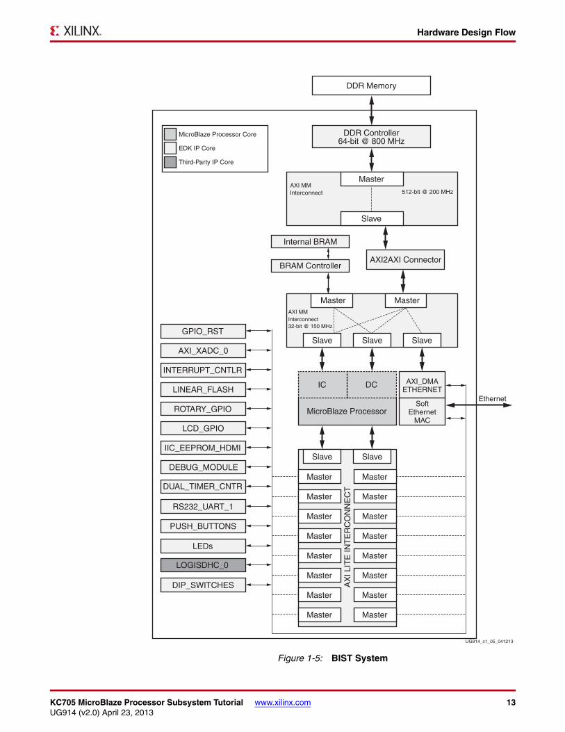
KC705 MicroBlaze Processor Subsystem Tutorial www.xilinx.com 13UG914 (v2.0) April 23, 2013
Hardware Design Flow
X-Ref Target - Figure 1-5
Figure 1-5: BIST System
UG914_c1_05_041213
DDR Memory
AXI2AXI Connector
DIP_SWITCHES
LOGISDHC_0
LEDs
PUSH_BUTTONS
RS232_UART_1
DUAL_TIMER_CNTR
DEBUG_MODULE
IIC_EEPROM_HDMI
LCD_GPIO
ROTARY_GPIO
LINEAR_FLASH
INTERRUPT_CNTLR
AXI_XADC_0
GPIO_RST
DDR Controller64-bit @ 800 MHz
MicroBlaze Processor Core
EDK IP Core
Third-Party IP Core
MasterAXI MMInterconnect 512-bit @ 200 MHz
Slave
MasterAXI MMInterconnect32-bit @ 150 MHz
SlaveSlave
SlaveSlave
Master Master
Master Master
Master Master
Master Master
Master Master
Master Master
Master Master
Master Master
IC
MicroBlaze Processor
DC AXI_DMAETHERNET
EthernetSoft
EthernetMAC
SlaveA
XI L
ITE
INT
ER
CO
NN
EC
T
Master
Internal BRAM
BRAM Controller

14 www.xilinx.com KC705 MicroBlaze Processor Subsystem TutorialUG914 (v2.0) April 23, 2013
Chapter 1: KC705 Embedded Kit MicroBlaze Processor Subsystem Hardware Tutorial
Examine the System
The System Assembly View (SAV) of the design provides visibility into the MicroBlaze processor subsystem bus interfaces, port connections, and address map.
Note: Refer to UG683, EDK Concepts, Tools, and Techniques for additional details or instructions pertaining to any of the steps outlined in this section of the tutorial.
Examine Bus Interfaces
1. To examine the bus structure of the MicroBlaze processor subsystem, select the System Assembly View tab below the workspace and then select the Bus Interfaces tab at the top edge of the workspace as shown in Figure 1-6.
For MicroBlaze processor masters (Instruction Cache (IC), Data Cache (DC), and Data Port (DP)), both AXI_MM and AXI_Lite interconnects are used. Two Local Memory Buses (LMB) are used by the MicroBlaze processor to interface to the local BRAM memory for the processor. These interfaces can be seen by clicking the + to the left of the microblaze_0 component. (See: Figure 1-6).
X-Ref Target - Figure 1-6
Figure 1-6: Bus Interfaces View of the MicroBlaze Processor Subsystem
UG914_c1_06_032313

KC705 MicroBlaze Processor Subsystem Tutorial www.xilinx.com 15UG914 (v2.0) April 23, 2013
Hardware Design Flow
Examine Ports
1. Select the Ports tab along the top edge of the workspace. By clicking the + to the left of any of the components, the connections to that component are visible. (See: Figure 1-7)
Note: The visibility of the port connections for the system is controlled by the Port Filters as shown in Figure 1-8. Many of the peripherals have only default port connections to the AXI interconnect and these connections are not shown unless Defaults filter item is checked.
X-Ref Target - Figure 1-7
Figure 1-7: Ports View of the MicroBlaze Processor Subsystem
UG914_c1_07_032313
X-Ref Target - Figure 1-8
Figure 1-8: Port Filters
UG914_c1_08_071812

16 www.xilinx.com KC705 MicroBlaze Processor Subsystem TutorialUG914 (v2.0) April 23, 2013
Chapter 1: KC705 Embedded Kit MicroBlaze Processor Subsystem Hardware Tutorial
Examine Addresses
1. Select the Addresses tab along the top edge of the workspace. Click the + to the left of the microblaze_0 address map to expand the map as shown in Figure 1-9. This workspace is used to modify the addresses of peripherals in the system.
Configure IP Cores
The IP cores within the system are configured to the required functionality for this embedded system. The configurations of the IP cores are described in the System Configuration section of DS669, AXI Interface Based KC705 Embedded Kit MicroBlaze Processor Subsystem Data Sheet.
1. With the Bus Interfaces tab selected in the System Assembly view, right-click the IP core of interest, as shown in Figure 1-10.
X-Ref Target - Figure 1-9
Figure 1-9: Addresses View of the MicroBlaze Processor Subsystem
UG914_c1_09_080612

KC705 MicroBlaze Processor Subsystem Tutorial www.xilinx.com 17UG914 (v2.0) April 23, 2013
Hardware Design Flow
2. Select Configure IP... and the configuration wizard for that core is displayed. Select the tab to show the particular feature or parameter of interest. Figure 1-11 shows the configuration wizard for the Dual_Timer_Counter core.
X-Ref Target - Figure 1-10
Figure 1-10: Menu Option to Configure IP
UG914_c1_10_032313

18 www.xilinx.com KC705 MicroBlaze Processor Subsystem TutorialUG914 (v2.0) April 23, 2013
Chapter 1: KC705 Embedded Kit MicroBlaze Processor Subsystem Hardware Tutorial
3. Click Cancel to return to the System Assembly View since no changes are needed to the cores in the system at this time.
Generate the Hardware Platform
1. Close the XPS project by selecting File > Exit.
2. In the Project Manager/Sources pane, click system_top - STRUCTURE.
3. In the Flow Navigator pane, double click Generate Bitstream under the Program and Debug section, as shown in Figure 1-12.
Note: Because the design is not yet implemented, a message window will open to indicate that no implementation results are available. Click Yes to close the message window.
X-Ref Target - Figure 1-11
Figure 1-11: Dual Timer Counter - AXI_Timer Configuration Wizard
UG914_c1_11_072012

KC705 MicroBlaze Processor Subsystem Tutorial www.xilinx.com 19UG914 (v2.0) April 23, 2013
Hardware Design Flow
Export the BIST Hardware Platform to SDKBecause the BIST hardware platform is used with the Software Development Kit (SDK) as described in UG915, AXI Interface Based KC705 Embedded Kit MicroBlaze Processor Subsystem Software Tutorial, information about the hardware platform must be provided to the SDK to allow development of software platforms and applications. Use the following steps to export this information to the SDK:
1. When bitstream generation is complete:
a. In the Flow Navigator pane, double click Open Implemented Design under the Implementation section.
b. Under Sources, click system_i - system (system.xmp).
c. Under the File tab, select Export and click Export Hardware to open the dialog shown in Figure 1-13.
X-Ref Target - Figure 1-12
Figure 1-12: Generating the Hardware Bitstream
UG914_c1_12_032313

20 www.xilinx.com KC705 MicroBlaze Processor Subsystem TutorialUG914 (v2.0) April 23, 2013
Chapter 1: KC705 Embedded Kit MicroBlaze Processor Subsystem Hardware Tutorial
d. The exported hardware description files are stored in this location:KC705_Embedded_Kit/Tutorial_Sandbox/HW/BIST/kc705_system.sdk/SDK/SDK_Export
2. Copy the SDK_Export directory into the SW area of the Tutorial sandbox for use with the procedure described in UG915, AXI Interface Based KC705 Embedded Kit MicroBlaze Processor Subsystem Software Tutorial. The existing directory can be overwritten.
Copy:
KC705_Embedded_Kit/Tutorial_Sandbox/HW/BIST/kc705_system.sdk/SDK/SDK_Export
to:
KC705_Embedded_Kit/Tutorial_Sandbox/SW/board_test_app
The SDK is run using the procedure described in UG915, AXI Interface Based KC705 Embedded Kit MicroBlaze Processor Subsystem Software Tutorial.
Download and Verify BIST Design
1. The steps for testing the newly generated bit file are the same as those used to generate the System section where pre built bit and ELF files are tested. The only difference is that the new bit file should be loaded from KC705_Embedded_Kit/Tutorial_Sandbox/HW/BIST/kc705_system.runs/impl_1/download.bit
2. The UART output will be displayed and should look similar to Figure 1-4, page 11.
3. Execute the chosen tests and then select 0 to exit. Refer to UG915, AXI Interface Based KC705 Embedded Kit MicroBlaze Processor Subsystem Software Tutorial for details about these test options.
At this point in the tutorial, the KC705 embedded kit MicroBlaze processor subsystem is successfully built, verified, and exported for use with the SDK. The next section in this tutorial explains how to customize an embedded hardware platform. Alternately, if no modifications to the hardware subsystem are required, proceed with the tutorial presented in UG915, KC705 Embedded Kit MicroBlaze Processor Subsystem Software Tutorial.
X-Ref Target - Figure 1-13
Figure 1-13: Exporting BIST Hardware Platform to SDK
UG914_c1_13_071812

KC705 MicroBlaze Processor Subsystem Tutorial www.xilinx.com 21UG914 (v2.0) April 23, 2013
Hardware Design Flow
Customize the Embedded Hardware PlatformIn this section of the tutorial, the partially built video demo system from the Tutorial Sandbox directory is modified to include an additional AXI_VDMA for developing a complete video system. After building the hardware, the video demonstration application uses a Web server to display the video throughput data.
Every data point consists of a data transfer of a gigabyte by means of multiple AXI Video DMAs. Each Video DMA transfers the video data to and from the DDR memory through the AXI interconnect and the DDR controller. The Perf_AXI core monitors the transactions on the AXI interface to provide data throughput calculations.
Note: For More details on the video demo, refer to DS669, AXI Interface Based KC705 Embedded Kit MicroBlaze Processor Subsystem Data Sheet.
The steps to customize the MicroBlaze processor subsystem include:
1. Add IP from the Xilinx IP Catalog.
Note: The VDMA which will be added to the partially built video demo system is highlighted in Figure 1-14.
2. Connect the Bus Interfaces.
3. Connect the Ports.X-Ref Target - Figure 1-14
Figure 1-14: Video Demo MicroBlaze Processor Subsystem
MICROBLAZESCALER_0 VDMA
AXI MMINTERCONNECT
32bit@150 MHz
DDR
DDR CONTROLLER64bit@800MHz
SLAVE SLAVE
MASTERAXI MMINTERCONNECT
512bit@150 MHz
SLAVE SLAVE SLAVE SLAVE
MASTER AXI MMINTERCONNECT
512bit@150 MHz
SLAVE SLAVE SLAVESLAVE
MASTER
AXI2AXI CONNECTOR AXI2AXI CONNECTOR AXI2AXI CONNECTOR
MASTER
SLAVESLAVE SLAVE SLAVE
DVI_0 VDMAS2MM
MM2STPG_0VDMA_S2MM
S2MM IC DC
AXITPG_0
AXITPG_2
TIME BASEGENERATOR
SCALER_2 VDMA
MM2S S2MM
DVI_1 VDMAS2MM
TPG_2VDMA_S2MM
S2MM S2MM
DVI2AXI
DVI2AXI
FMC DVI IN(1920x1080)
(1080p)
FMC DVI IN(1920x1080)
(1080p)
DVI_SCALAR
DVI_SCALAR
AXI_SCALAR AXI_SCALARSLAVE SLAVE
MASTER
MASTER
MASTER
MASTER
MASTER
MASTER
MASTER
MASTER
MASTER
MASTER
LOGIC CVC
MASTER
MASTER
MASTER
MASTER
MASTER
MASTER
MASTER
MASTER
MASTER
MASTER
MASTER
MASTER
SLAVE
AX
I2AX
I CO
NN
EC
TO
R
PERF_MONITOR_0
INTERRUPT_CNTLR
3.8 Gb/s 3.8 Gb/s 1 Gb/s1 Gb/s 3.8 Gb/s1 Gb/s 1 Gb/s3.8 Gb/s
3.8 Gb/s
IIC
23 Gb/s
MASTER
MICROBLAZE EDK IP CORE
EDK IP CORE
LOCAL PCORE
THIRD PARTY IP CORE
AXI_TPG_DVI_0
VIDEO_MUX_0
AXI_TPG_DVI_1
VIDEO_MUX_1
LINEAR_FLASH
ROTARY_GPIO
LCD_GPIO
LEDS
PUSH_BUTTONS
RS232_UART_1
DUAL_TIMER_CNTR
DEBUG_MODULE
IIC_EEPROM_HDMI
AXI_XADC_0
LOGISDHC_0
GPIO_RST
HDMI_OUT1920x1080
ADV7511HDMI
SLAVE
AXI_DMAETHERNET
SOFTETHERNET
MAC
MASTER
DIP_SWITCHES
Ethernet
MASTER
MASTER
MASTER
MASTER
MASTER
MASTER
512bit@200 MHz
AX
I LITE
INT
ER
CO
NN
EC
T
AX
I LITE
INT
ER
CO
NN
EC
T
UG914_c1_14_041213
MASTER
Internal BRAM
BRAM Controller

22 www.xilinx.com KC705 MicroBlaze Processor Subsystem TutorialUG914 (v2.0) April 23, 2013
Chapter 1: KC705 Embedded Kit MicroBlaze Processor Subsystem Hardware Tutorial
Add IP from the Xilinx IP Catalog
To Add the AXI VDMA Core:
1. The PlanAhead tool should already be running (from the previous section of this tutorial).
2. Close the BIST project by selecting File > Close Project.
3. In Project Commands, select Open Project...
4. Browse to KC705_Embedded_Kit/Tutorial_Sandbox/HW/Video_Demo and select video_demo.ppr. Click OK.
5. Under Sources, expand Design Sources and system_top -STRUCTURE and double click system_i - system (system.xmp). This invokes XPS for the XPS subsystem.
6. In the EDK_Install section, Expand the DMA and Timer list by clicking the respective +. The AXI Video DMA IP core is now displayed.
Note: The description field can be made wider by placing the cursor near the divider between the fields until it changes into two vertical bars with two opposing horizontal arrows. Click and drag to adjust the width.
7. Right-click the AXI Video DMA and select Add IP, as shown in Figure 1-15.
Note: Warning messages about the axi_vdma or other cores added into the system not being accessible from any processor in the system can be safely ignored. The procedure to connect the bus interfaces is discussed later in this tutorial.
X-Ref Target - Figure 1-15
Figure 1-15: Adding the AXI_VDMA Core
UG914_c1_15_032313

KC705 MicroBlaze Processor Subsystem Tutorial www.xilinx.com 23UG914 (v2.0) April 23, 2013
Hardware Design Flow
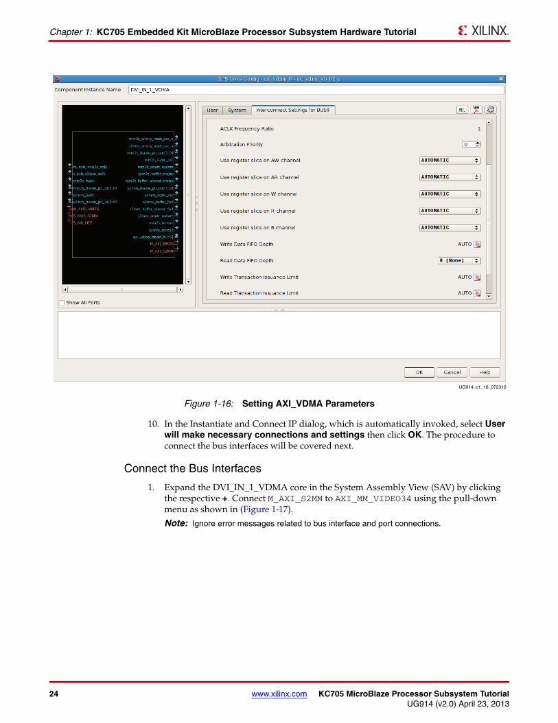
8. The XPS Core Configuration dialog is automatically invoked (See: Figure 1-16, page 24). This dialog sets AXI interconnect parameters for the core such as register slicing.
9. In the Configuration dialog, make the following settings:
• Component instance name: DVI_IN_1_VDMA
• In the USER tab:
- Select Enable Asynchronous Clocks within the VDMA options
- Clear Enable Channel within MM2S Channel options
• Do following changes within the S2MM Channel options:
- Set Memory Map Data Width as 64 from pull down menu
- Select Allow Unaligned Transfers (DRE)
- Set Maximum Burst Size to 256 from pull down menu
- Set Line Buffer Depth to 4096
• In the SYSTEM tab:
- Base Address: 0x50900000
- High Address: 0X5090FFFF
• In the Interconnect Settings for BUSIF tab, M_AXI_S2MM section
- User Register Slice on all channels (AW,AR,W,R and B): AUTOMATIC
- Write Data FIFO Depth: 512 (BRAM)
• In Interconnect Settings for BUSIF tab, S_AXI_LITE section
- User Register Slice on all channels (AW,AR,W,R and B): AUTOMATIC
• Click Ok
24 www.xilinx.com KC705 MicroBlaze Processor Subsystem TutorialUG914 (v2.0) April 23, 2013
Chapter 1: KC705 Embedded Kit MicroBlaze Processor Subsystem Hardware Tutorial
10. In the Instantiate and Connect IP dialog, which is automatically invoked, select User will make necessary connections and settings then click OK. The procedure to connect the bus interfaces will be covered next.
Connect the Bus Interfaces
1. Expand the DVI_IN_1_VDMA core in the System Assembly View (SAV) by clicking the respective +. Connect M_AXI_S2MM to AXI_MM_VIDEO34 using the pull-down menu as shown in (Figure 1-17).
Note: Ignore error messages related to bus interface and port connections.
X-Ref Target - Figure 1-16
Figure 1-16: Setting AXI_VDMA Parameters
UG914_c1_16_072312

KC705 MicroBlaze Processor Subsystem Tutorial www.xilinx.com 25UG914 (v2.0) April 23, 2013
Hardware Design Flow
2. For S_AXI_LITE, click the No Connection box. The Connection Dialog box appears. In the left column, select AXI4Lite_0 as shown in Figure 1-18 and click OK.
X-Ref Target - Figure 1-17
Figure 1-17: Connecting DVI_IN_1VDMA Master Interface to AXI MM interconnect
UG914_c1_17_032313
X-Ref Target - Figure 1-18
Figure 1-18: Connecting DVI_IN_1VDMA Lite Slave Interface to AXI Lite interconnect
UG914_c1_18_032313

26 www.xilinx.com KC705 MicroBlaze Processor Subsystem TutorialUG914 (v2.0) April 23, 2013
Chapter 1: KC705 Embedded Kit MicroBlaze Processor Subsystem Hardware Tutorial
3. Connect S_AXIS_S2MM to DVI_IN_1_S_AXIS_S2MM using the pull-down menu as shown in Figure 1-19.
4. Expand the axi2axi_video34 core in the Bus Interface tab of System Assembly View of the XPS GUI by clicking the respective +.
5. Click the Bus Name column for the S_AXI row. This brings up the master list dialog for the axi2axi_video34 connector.
6. Select DVI_IN_1_VDMA.M_AXIS_S2MM and click OK (see Figure 1-20).
X-Ref Target - Figure 1-19
Figure 1-19: Connecting DVI_IN_1VDMA Stream Slave Interface to Video Streaming Master
UG914_c1_19_032313

KC705 MicroBlaze Processor Subsystem Tutorial www.xilinx.com 27UG914 (v2.0) April 23, 2013
Hardware Design Flow
Connect the Ports
The section covers connecting clock pins, interrupts, and signals for the DVI_IN_1_VDMA. In the Port Filters section of the XPS window, ensure that Defaults is selected (refer to Figure 1-8, page 15).
1. Click the Ports tab at the top of the System Assembly View.
2. Expand the DVI_IN_1_VDMA core in the System Assembly View by clicking the respective +.
3. In the name column of the port list for s_axis_s2mm_aclk, select the net name sys_clk_s using the pull-down menu.
4. Expand (BUS_IF) S_AXI_Lite by clicking the respective +. In the name column for s_axi_lite_aclk, select the net name sys_clk_axilite_s using the pull-down menu in the Net column.
5. Expand (BUS_IF) M_AXI_S2MM by clicking the respective +. In the name column for m_axi_s2mm_aclk, select the net name sys_clk_s using the pull-down menu.
6. Expand (BUS_IF) S_AXIS_S2MM by clicking the respective +. In the name column for s_axis_s2mm_tdata, enter the new connection name, 0x00 & dvi2axi_tdata_1.
7. In the name column for s2mm_fsync_out, enter the new connection name, fsync_from_dvi_in_1_vdma.
8. In the name column for s2mm_introut, enter the new connection name, DVI_IN_1_VDMA_s2mm_introut.
9. In the name column for s2mm_prmry_reset_out_n, enter the new connection name, DVI_IN_1_S_AXIS_S2MM_RESET_OUT_N.
10. Expand the Interrupt_Cntlr core in the System Assembly view by clicking the respective +.
X-Ref Target - Figure 1-20
Figure 1-20: Adding DVI_IN_1VDMA as AXI MM Master to AXI2AXI Connector
UG914_c1_20_032313
28 www.xilinx.com KC705 MicroBlaze Processor Subsystem TutorialUG914 (v2.0) April 23, 2013
Chapter 1: KC705 Embedded Kit MicroBlaze Processor Subsystem Hardware Tutorial
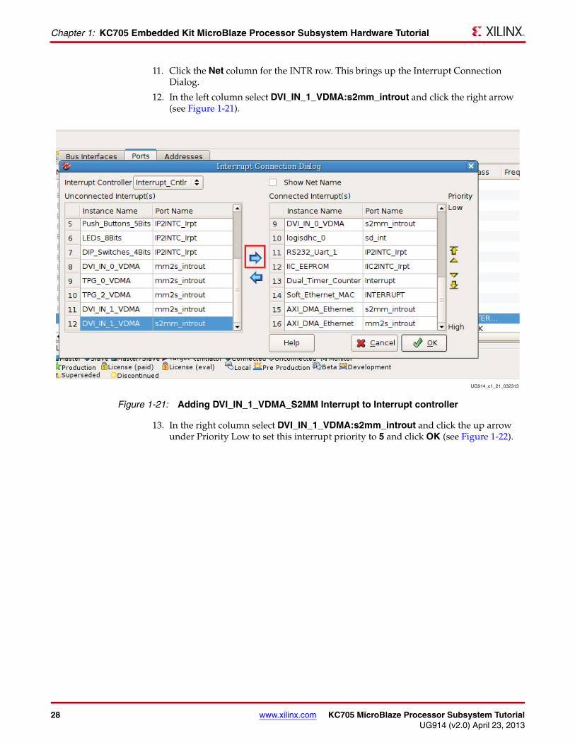
11. Click the Net column for the INTR row. This brings up the Interrupt Connection Dialog.
12. In the left column select DVI_IN_1_VDMA:s2mm_introut and click the right arrow (see Figure 1-21).
13. In the right column select DVI_IN_1_VDMA:s2mm_introut and click the up arrow under Priority Low to set this interrupt priority to 5 and click OK (see Figure 1-22).
X-Ref Target - Figure 1-21
Figure 1-21: Adding DVI_IN_1_VDMA_S2MM Interrupt to Interrupt controller
UG914_c1_21_032313

KC705 MicroBlaze Processor Subsystem Tutorial www.xilinx.com 29UG914 (v2.0) April 23, 2013
Hardware Design Flow
14. As shown in Figure 1-23 Double click axi_mm_video34 to open the configuration wizard
15. Select Master Read/Write Settings and click the Master/Slave Specific Settings tab.
16. Set Write FIFO Delay for DVI_IN_1_VDMA.M_AXI_S2MM to 1 and press OK.
X-Ref Target - Figure 1-22
Figure 1-22: Setting DVI_IN_1_VDMA_S2MM Interrupt priority
UG914_c1_22_032313

30 www.xilinx.com KC705 MicroBlaze Processor Subsystem TutorialUG914 (v2.0) April 23, 2013
Chapter 1: KC705 Embedded Kit MicroBlaze Processor Subsystem Hardware Tutorial
At this point in the tutorial, additional IP from the Xilinx IP Catalog has successfully been added to the KC705 embedded kit MicroBlaze processor subsystem.
Implement and Test the DesignThe design is ready to be synthesized, mapped, placed and routed in the chosen FPGA architecture.
1. Close the XPS project by selecting File > Exit.
2. Under Project Manager/Sources, click system_top - STRUCTURE.
3. In the Flow Navigator, double click Generate Bitstream under the Program and Debug section, as shown in Figure 1-12, page 19.
4. Once the bit file is generated, Export hardware to SDK as explained in Export the BIST Hardware Platform to SDK, page 19.
5. Connect the FMC cards, HDMI cables, Ethernet cable and USB cables as shown in UG913, Getting Started with the Kintex-7 FPGA KC705 Embedded Kit, Kintex-7 FPGA Video Demonstration Hardware Setup.
6. Configure the FPGA with the generated bit file, KC705_Embedded_Kit/Tutorial_Sandbox/HW/Video_Demo/MicroBlaze_Processor_Subsystem/download.bit
X-Ref Target - Figure 1-23
Figure 1-23: DVI_IN_1_VDMA Interconnect settings
UG914_c1_23_071812

KC705 MicroBlaze Processor Subsystem Tutorial www.xilinx.com 31UG914 (v2.0) April 23, 2013
Summary
7. Load and run the software ELF file, KC705_Embedded_Kit/Video_Demo/ready_for_download/Video_Demo.elf
8. Open the webpage at IP 192.168.1.10 which shows the video demo web server running on the MicroBlaze processor subsystem.
9. Select different menu options on the web page and check the video output and data throughput for different possible options.
Note: For more details on Video Demo testing, different possible menu options and data throughput values refer to UG913, Getting Started with the Kintex-7 FPGA KC705 Embedded Kit.
SummaryThe tasks accomplished in this tutorial are listed here:
• Loaded and executed a design from a pre-built bitstream and ELF
• Rebuilt a design
• Added IP from the Xilinx IP catalog to an embedded system
Next Steps
Next Step Refer To
Develop the Software Platform UG915, AXI Interface Based KC705 Embedded Kit MicroBlaze Processor Subsystem Software Tutorial
Advanced Debugging UG029, ChipScope Pro Software and Cores User Guide and UG111, Embedded System Tools Reference Manual, GNU compiler tools
Simulate the Embedded System UG683, EDK Concepts, Tools, and Techniques

32 www.xilinx.com KC705 MicroBlaze Processor Subsystem TutorialUG914 (v2.0) April 23, 2013
Chapter 1: KC705 Embedded Kit MicroBlaze Processor Subsystem Hardware Tutorial

KC705 MicroBlaze Processor Subsystem Tutorial www.xilinx.com 33UG914 (v2.0) April 23, 2013
Appendix A
Additional Resources
Xilinx ResourcesFor support resources such as Answers, Documentation, Downloads, and Forums, see the Xilinx Support website at:
www.xilinx.com/support.
For continual updates, add the Answer Record to your myAlerts:
www.xilinx.com/support/myalerts.
For a glossary of technical terms used in Xilinx documentation, see:
www.xilinx.com/company/terms.htm.
Solution CentersSee the Xilinx Solution Centers for support on devices, software tools, and intellectual property at all stages of the design cycle. Topics include design assistance, advisories, and troubleshooting tips.
Further ResourcesThe most up to date information related to the KC705 board and its documentation is available on the following websites.
The Xilinx Kintex-7 FPGA Embedded Kit product page:
www.xilinx.com/products/boards-and-kits/DK-K7-EMBD-G.htm
The Kintex-7 FPGA Embedded Kit - Known Issues and Release Notes Master Answer Record:
www.xilinx.com/support/answers/52970.htm
These documents provide supplemental material useful with this user guide:
• UG913, Getting Started with the Kintex-7 FPGA KC705 Embedded Kit
• UG683, EDK Concepts, Tools, and Techniques
• DS669, AXI Interface Based KC705 Embedded Kit MicroBlaze Processor Subsystem Data Sheet
• UG111, Embedded System Tools Reference Manual
• UG915, AXI Interface Based KC705 Embedded Kit MicroBlaze Processor Subsystem Software Tutorial
• UG029, ChipScope Pro Software and Cores User Guide
34 www.xilinx.com KC705 MicroBlaze Processor Subsystem TutorialUG914 (v2.0) April 23, 2013
Appendix A: Additional Resources
• UG631, ISE Design Suite 14: Release Notes, Installation, and Licensing
• UG810, KC705 Evaluation Board for the Kintex-7 FPGA User Guide
• UG081, MicroBlaze Processor Reference Guide Embedded Development Kit
ReferencesAMBA AXI4-Stream Protocol Specification:
infocenter.arm.com/help/index.jsp?topic=/com.arm.doc.ihi0051a/index.html


![Kintex-7 FPGA KC705 Evaluation Kit-KC705 Evaluation Board for the Kintex-7 FPGA User Guide (UG810) [Ref 1]-Kintex-7 FPGA KC705 Base Targeted Reference Design User Guide (UG882) [Ref](https://img.dokumen.tips/doc/110x75/5f6f6c0b693ef83e28062053/kintex-7-fpga-kc705-evaluation-kc705-evaluation-board-for-the-kintex-7-fpga-user.jpg)