Embed Size (px)
Citation preview
ITRSITRSAssembly and PackagingAssembly and Packaging
2007 Roadmap2007 Roadmap
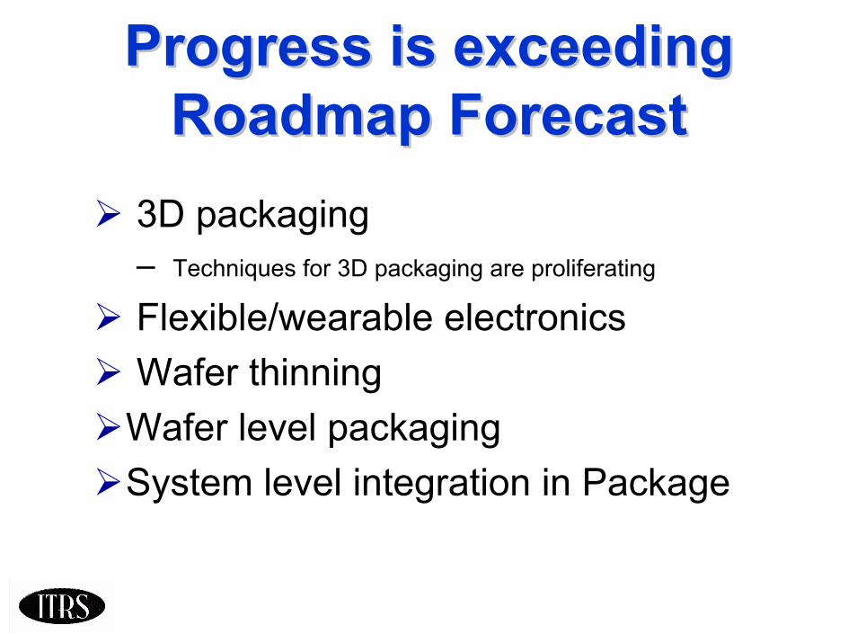
Progress is exceeding Progress is exceeding Roadmap ForecastRoadmap Forecast
3D packaging– Techniques for 3D packaging are proliferating
Flexible/wearable electronicsWafer thinningWafer level packagingSystem level integration in Package
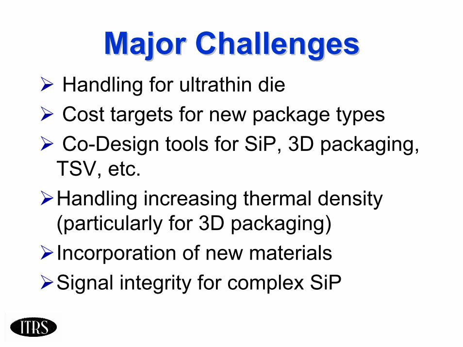
Major ChallengesMajor ChallengesHandling for ultrathin dieCost targets for new package typesCo-Design tools for SiP, 3D packaging, TSV, etc.Handling increasing thermal density (particularly for 3D packaging)Incorporation of new materialsSignal integrity for complex SiP
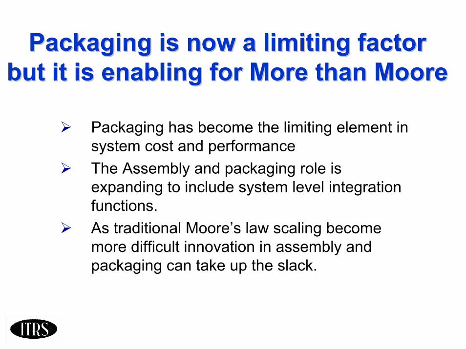
Packaging is now a limiting factorbut it is enabling for More than Moore
Packaging is now a limiting factorPackaging is now a limiting factorbut it is enabling for More than Moorebut it is enabling for More than Moore
Packaging has become the limiting element in system cost and performance The Assembly and packaging role is expanding to include system level integration functions.As traditional Moore’s law scaling become more difficult innovation in assembly and packaging can take up the slack.
Interacting with people and environmentNon-digital content System-in-Package (SiP)
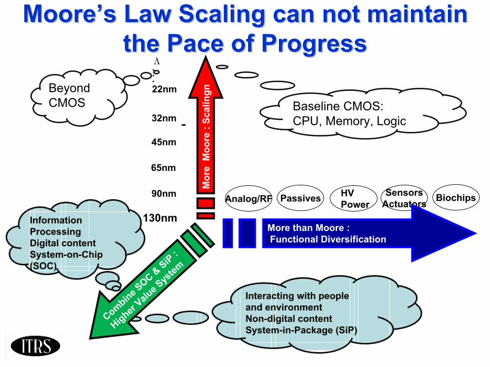
MooreMoore’’s Law Scaling can not maintain s Law Scaling can not maintain the Pace of Progress the Pace of Progress
Beyond CMOS
Information Processing Digital content System-on-Chip (SOC)
BiochipsSensorsActuators
HVPowerAnalog/RF Passives
More than Moore : Functional Diversification
130nm
90nm
65nm
45nm
32nm
Λ...22nm
Mor
e M
oore
: Sc
alin
gn
Combine SOC & SiP :
Higher Valu
e Sys
tem
Baseline CMOS: CPU, Memory, Logic
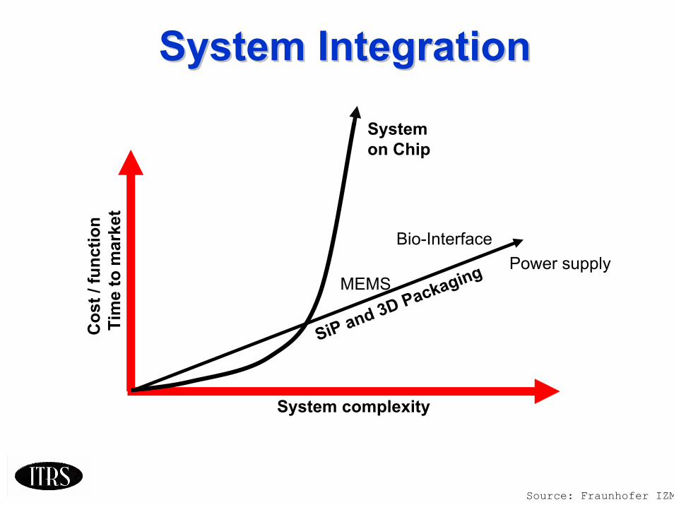
System IntegrationSystem IntegrationC
ost /
func
tion
Tim
e to
mar
ket
System on Chip
SiP and 3D PackagingMEMS
Bio-InterfacePower supply
System complexity
Source: Fraunhofer IZM
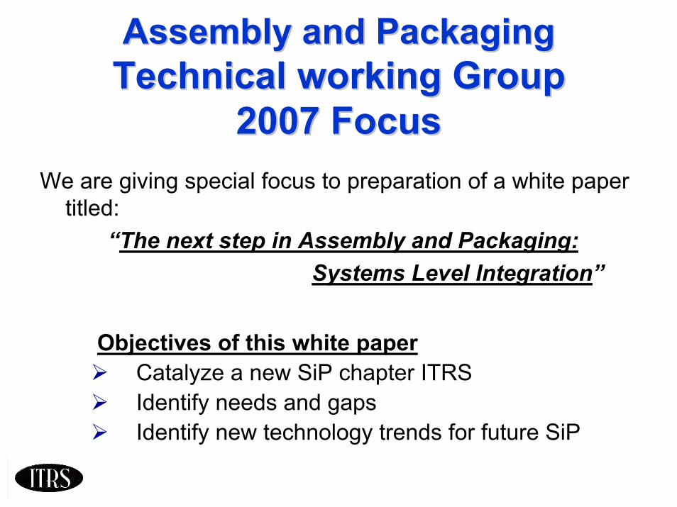
Assembly and Packaging Technical working Group
2007 Focus
Assembly and Packaging Assembly and Packaging Technical working Group Technical working Group
2007 Focus2007 FocusWe are giving special focus to preparation of a white paper
titled:“The next step in Assembly and Packaging:
Systems Level Integration”
Objectives of this white paperCatalyze a new SiP chapter ITRSIdentify needs and gaps Identify new technology trends for future SiP
SystemSystem--in Package definitionin Package definition
System in Package (SiP) is a combination of multiple active electronic components of different functionality, assembled into a
single unit, that provides multiple functions associated with a system or sub-system. An SiP may optionally contain passives,
MEMS, optical components and other packages and devices.
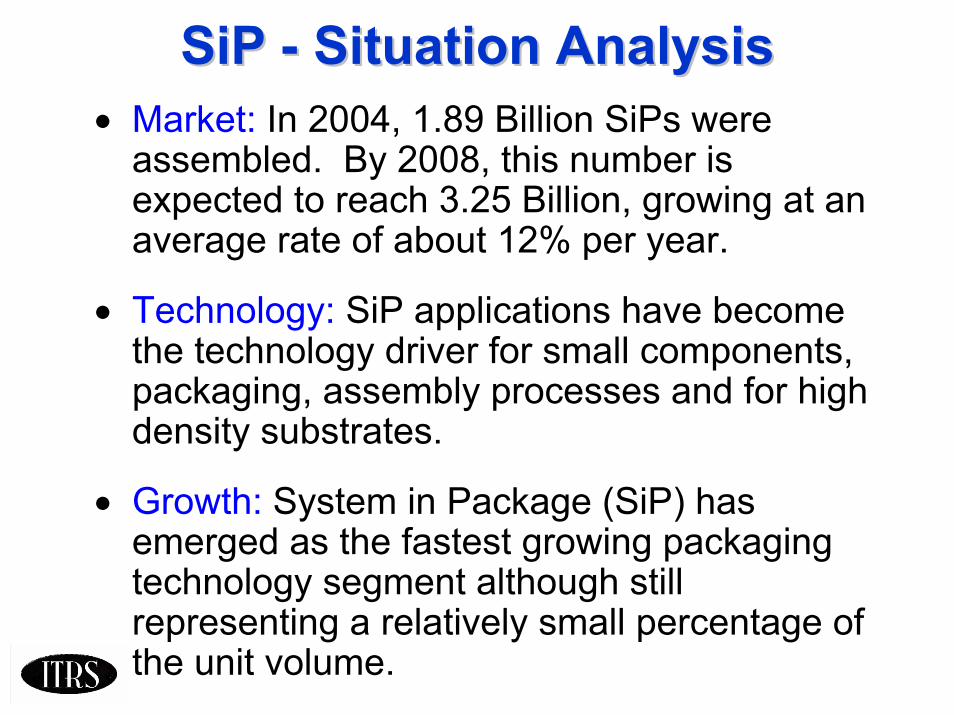
SiP SiP -- Situation AnalysisSituation Analysis• Market: In 2004, 1.89 Billion SiPs were
assembled. By 2008, this number is expected to reach 3.25 Billion, growing at an average rate of about 12% per year.
• Technology: SiP applications have become the technology driver for small components, packaging, assembly processes and for high density substrates.
• Growth: System in Package (SiP) has emerged as the fastest growing packaging technology segment although still representing a relatively small percentage of the unit volume.
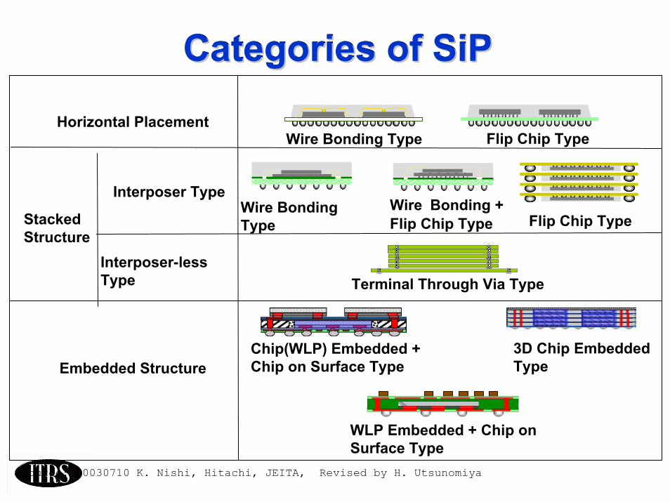
Categories of SiPCategories of SiPCategories of SiP
Horizontal Placement
StackedStructure
Interposer Type
Interposer-less Type
Wire Bonding Type Flip Chip Type
Wire Bonding Type
Wire Bonding +Flip Chip Type Flip Chip Type
Terminal Through Via Type
Embedded StructureChip(WLP) Embedded + Chip on Surface Type
3D Chip EmbeddedType
WLP Embedded + Chip on Surface Type
Source: 20030710 K. Nishi, Hitachi, JEITA, Revised by H. Utsunomiya
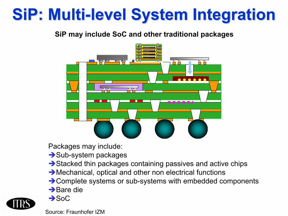
SiP: Multi-level System IntegrationSiP: MultiSiP: Multi--level System Integrationlevel System IntegrationSiP may include SoC and other traditional packages
Packages may include:Sub-system packages Stacked thin packages containing passives and active chipsMechanical, optical and other non electrical functionsComplete systems or sub-systems with embedded componentsBare dieSoC
Source: Fraunhofer IZM
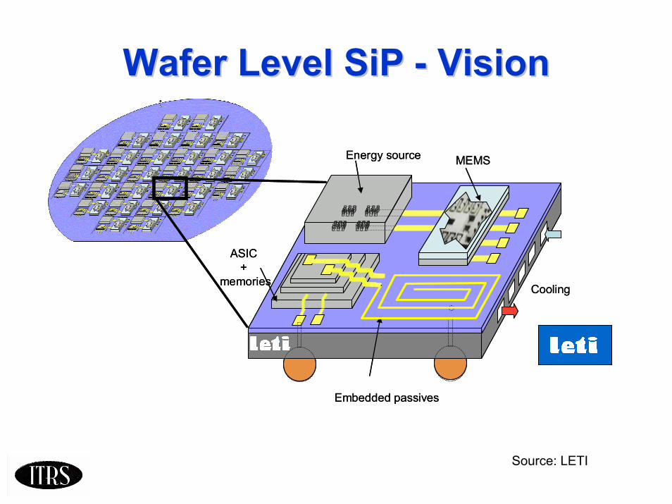
Wafer Level SiP Wafer Level SiP -- VisionVision
MEMSEnergy source
ASIC +
memories
Embedded passives
Cooling
MEMSEnergy source
ASIC +
memories
Embedded passives
Cooling
Source: LETI
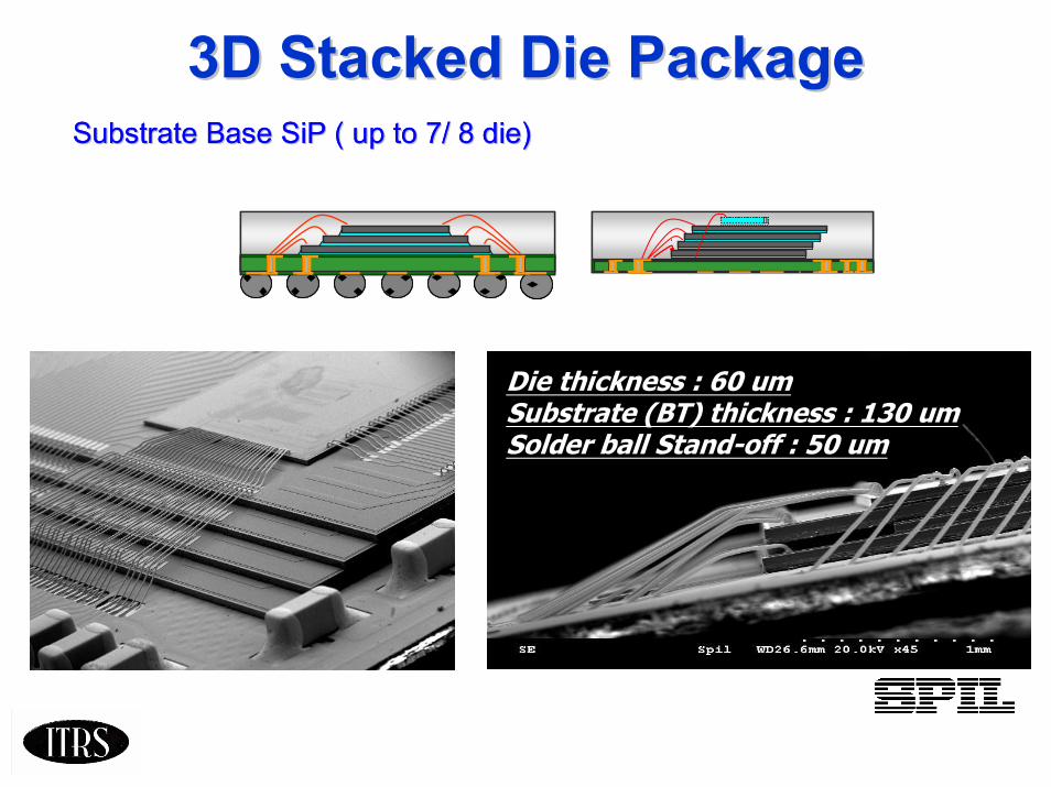
3D Stacked Die Package3D Stacked Die Package
Die thickness : 60 umSubstrate (BT) thickness : 130 umSolder ball Stand-off : 50 um
Substrate Base Substrate Base SiPSiP ( up to 7/ 8 die)( up to 7/ 8 die)
Die thickness : 60 umSubstrate (BT) thickness : 130 umSolder ball Stand-off : 50 um
Substrate Base Substrate Base SiPSiP ( up to 7/ 8 die)( up to 7/ 8 die)
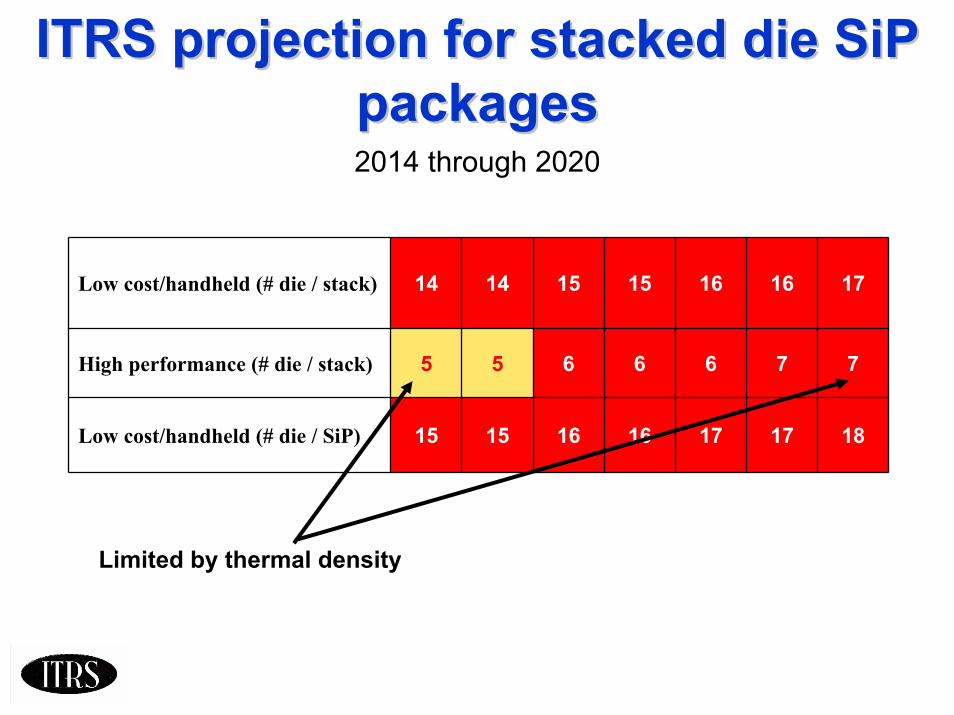
ITRS projection for stacked die SiP ITRS projection for stacked die SiP packages packages 2014 through 2020
Low cost/handheld (# die / stack) 14 14 15 15 16 16 17
High performance (# die / stack) 5 5 6 6 6 7 7
Low cost/handheld (# die / SiP) 15 15 16 16 17 17 18
Limited by thermal density
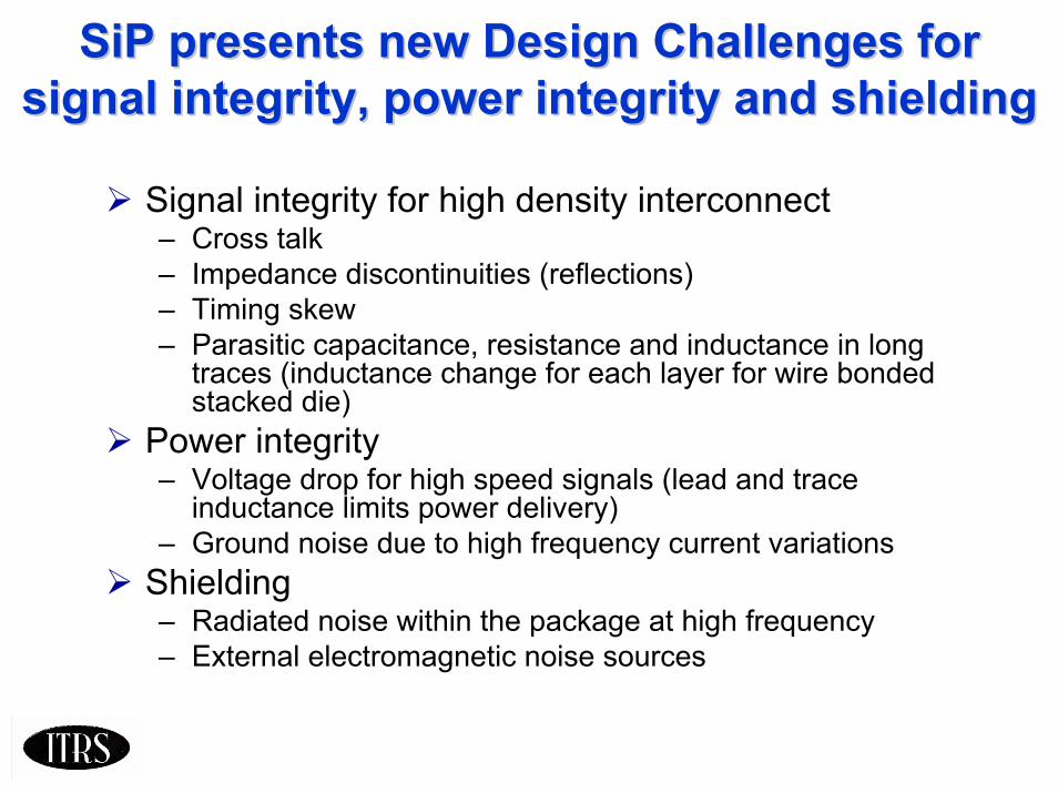
SiP presents new Design Challenges for SiP presents new Design Challenges for signal integrity, power integrity and shieldingsignal integrity, power integrity and shielding
Signal integrity for high density interconnect – Cross talk– Impedance discontinuities (reflections)– Timing skew– Parasitic capacitance, resistance and inductance in long
traces (inductance change for each layer for wire bonded stacked die)
Power integrity– Voltage drop for high speed signals (lead and trace
inductance limits power delivery)– Ground noise due to high frequency current variations
Shielding– Radiated noise within the package at high frequency– External electromagnetic noise sources
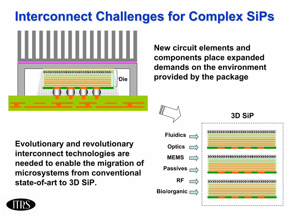
Interconnect Challenges for Complex Interconnect Challenges for Complex SiPsSiPs
Die
MEMS
Passives
RF
Fluidics
Optics
Bio/organic
3D SiP
Evolutionary and revolutionary interconnect technologies are needed to enable the migration of microsystems from conventional state-of-art to 3D SiP.
New circuit elements and components place expanded demands on the environment provided by the package
Potential Solutions for Potential Solutions for Interconnect ChallengesInterconnect Challenges
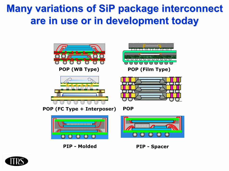
Many variations of SiP package interconnect Many variations of SiP package interconnect are in use or in development todayare in use or in development today
POP (WB Type)
POP (FC Type + Interposer)
POP (Film Type)
POP (only for Memory)
PIP - Molded PIP - Spacer
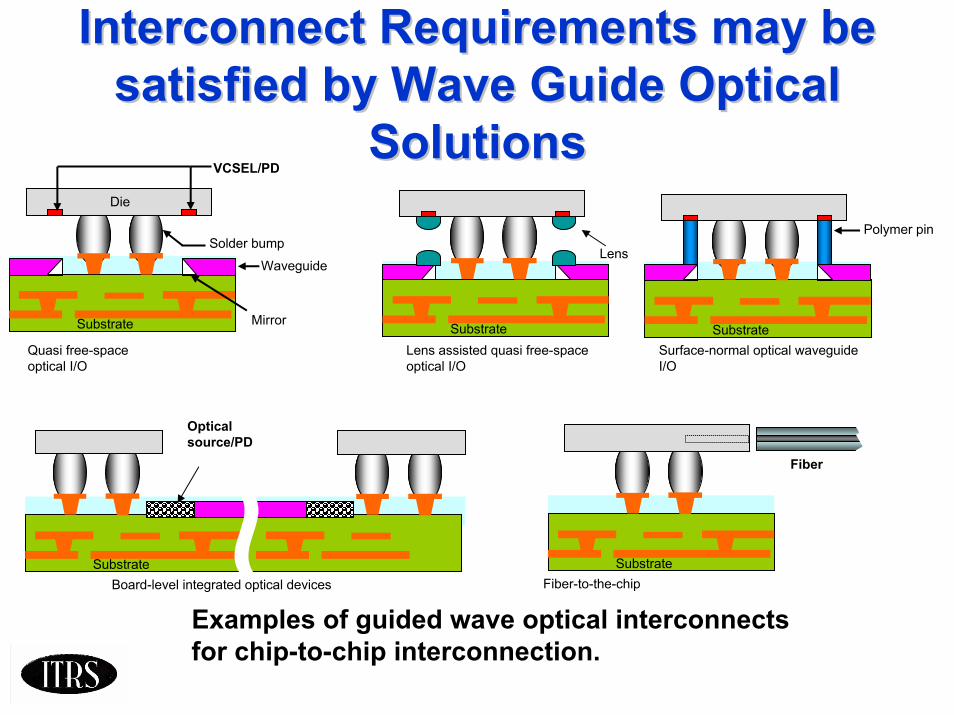
Interconnect Requirements may be Interconnect Requirements may be satisfied by Wave Guide Optical satisfied by Wave Guide Optical
SolutionsSolutions
Waveguide
Solder bump
Die
Mirror
VCSEL/PD
Substrate
Polymer pin
SubstrateSubstrate
Lens
Substrate Substrate
Fiber
Board-level integrated optical devices Fiber-to-the-chip
Quasi free-space optical I/O
Lens assisted quasi free-space optical I/O
Surface-normal optical waveguide I/O
Opticalsource/PD
Examples of guided wave optical interconnects for chip-to-chip interconnection.
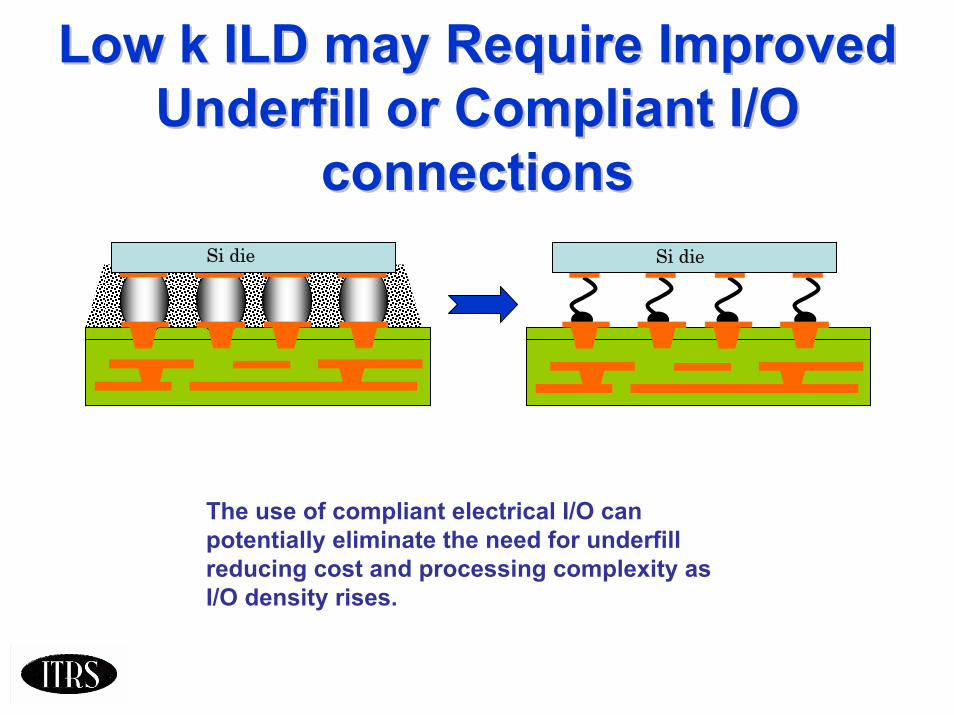
Low k ILD may Require Improved Low k ILD may Require Improved Underfill or Compliant I/O Underfill or Compliant I/O
connectionsconnectionsSi die Si die
The use of compliant electrical I/O can potentially eliminate the need for underfill reducing cost and processing complexity as I/O density rises.
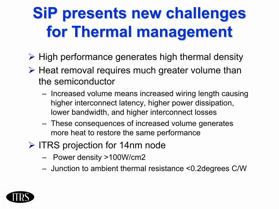
SiP presents new challenges SiP presents new challenges for Thermal management for Thermal management
High performance generates high thermal densityHeat removal requires much greater volume than the semiconductor– Increased volume means increased wiring length causing
higher interconnect latency, higher power dissipation, lower bandwidth, and higher interconnect losses
– These consequences of increased volume generates more heat to restore the same performance
ITRS projection for 14nm node– Power density >100W/cm2 – Junction to ambient thermal resistance <0.2degrees C/W
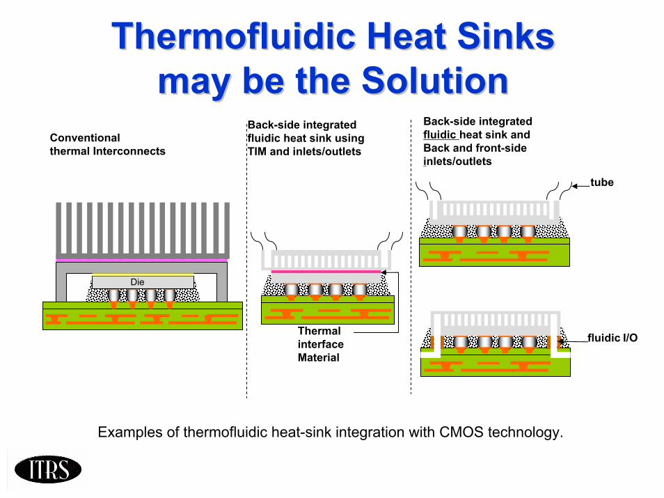
Thermofluidic Heat Sinks Thermofluidic Heat Sinks may be the Solutionmay be the Solution
Conventional thermal Interconnects
Back-side integratedfluidic heat sink and Back and front-side inlets/outlets
Thermal interface Material
Back-side integratedfluidic heat sink using TIM and inlets/outlets
tube
Die
fluidic I/O
Examples of thermofluidic heat-sink integration with CMOS technology.
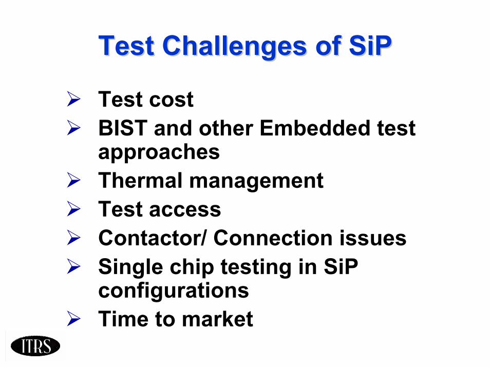
Test Challenges of SiPTest Challenges of SiP
Test costBIST and other Embedded test approachesThermal managementTest accessContactor/ Connection issuesSingle chip testing in SiP configurationsTime to market
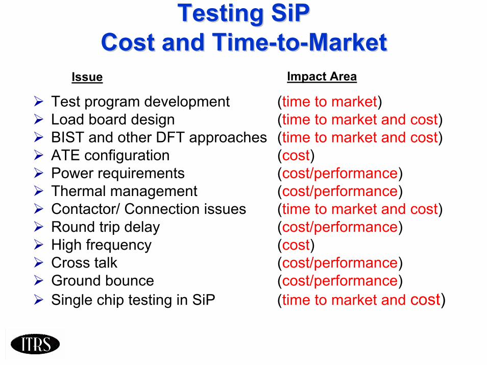
Testing SiPTesting SiPCost and TimeCost and Time--toto--Market Market
Impact AreaIssue
Test program development (time to market)Load board design (time to market and cost)BIST and other DFT approaches (time to market and cost)ATE configuration (cost)Power requirements (cost/performance)Thermal management (cost/performance)Contactor/ Connection issues (time to market and cost)Round trip delay (cost/performance)High frequency (cost)Cross talk (cost/performance)Ground bounce (cost/performance)Single chip testing in SiP (time to market and cost)
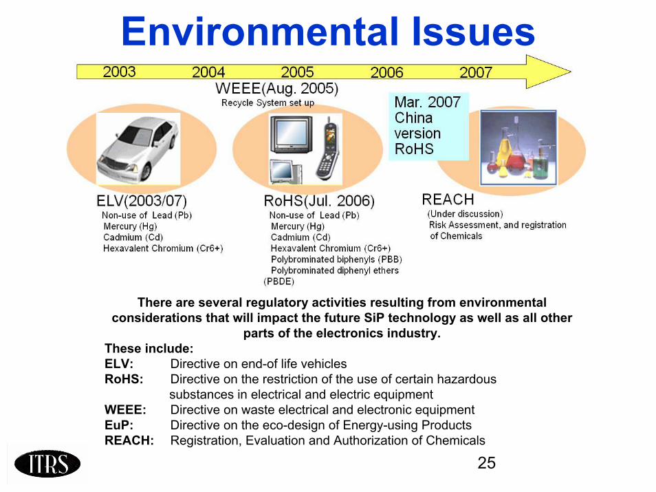
Environmental Issues
There are several regulatory activities resulting from environmental considerations that will impact the future SiP technology as well as all other
parts of the electronics industry. These include:ELV: Directive on end-of life vehiclesRoHS: Directive on the restriction of the use of certain hazardous
substances in electrical and electric equipmentWEEE: Directive on waste electrical and electronic equipmentEuP: Directive on the eco-design of Energy-using ProductsREACH: Registration, Evaluation and Authorization of Chemicals
25

Thank YouThank You


![International Technology Roadmap for Semiconductorsmaltiel-consulting.com/ITRS...Summary_2008_maltiel.pdf · 2008 ITRS Executive Summary Fig 5 [updated for 2007] Traditional . ORTC](https://img.dokumen.tips/doc/110x75/5f0ebd177e708231d440b30b/international-technology-roadmap-for-semiconductorsmaltiel-2008-itrs-executive.jpg)