Embed Size (px)
Citation preview
INTERNATIONAL TECHNOLOGY ROADMAP
FOR SEMICONDUCTORS
2009 EDITION
METROLOGY
THE ITRS IS DEVISED AND INTENDED FOR TECHNOLOGY ASSESSMENT ONLY AND IS WITHOUT REGARD TO ANY COMMERCIAL CONSIDERATIONS PERTAINING TO INDIVIDUAL PRODUCTS OR EQUIPMENT.
THE INTERNATIONAL TECHNOLOGY ROADMAP FOR SEMICONDUCTORS: 2009
TABLE OF CONTENTS Metrology.............................................................................................................................. 1
Scope...............................................................................................................................................2 Infrastructure Needs.....................................................................................................................................3
Critical Metrology Considerations ....................................................................................................3 Precision and Uncertainty ............................................................................................................................3 Sampling Requirements...............................................................................................................................4
Difficult Challenges ..........................................................................................................................5 Microscopy.......................................................................................................................................6 Lithography Metrology .....................................................................................................................7
Line Roughness .........................................................................................................................................10 Measurement Uncertainty ..........................................................................................................................10
Front End Processes Metrology ....................................................................................................14 Interconnect Metrology ..................................................................................................................18
3D Interconnect Issues and Metrology ......................................................................................................19 Cu-low κ Metallization Issues and Metrology Needs .................................................................................19 Low κ Dielectrics Issues and Metrology Needs .........................................................................................21
Materials and Contamination Characterization..............................................................................23 Reference Measurement System ..................................................................................................27
Reference Materials ...................................................................................................................................28 Integrated Metrology and Advanced Process Control ...................................................................29 Metrology for Emerging Research Materials and Devices.............................................................31
Update on Advances in Graphene Metrology............................................................................................31 3D Atomic Imaging and Spectroscopy.......................................................................................................31 Other Microscopy Needs including Scanning Probe Microscopy ..............................................................32 Optical Properties of Nanomaterials ..........................................................................................................33 Electrical Characterization for Emerging Materials and Devices ...............................................................34
References ....................................................................................................................................35
LIST OF FIGURES Figure MET1 Relations of Time, Tool, and Sample Dependent Components of
Uncertainty and Bias ........................................................................................4 Figure MET2a Lithography Metrology Potential Solutions: CD ..............................................13 Figure MET2b Lithography Metrology Potential Solutions: Overlay .......................................14 Figure MET3 Review of Stress/Strain Measurement Methods.............................................16 Figure MET4 3D Metrology Requirements ...........................................................................17 Figure MET5 FEP Metrology Potential Solutions .................................................................18 Figure MET6 Interconnect Metrology Potential Solutions ....................................................23 Figure MET7 Materials and Contamination Potential Solutions ...........................................27

LIST OF TABLES Table MET1 Metrology Difficult Challenges ..............................................................................5 Table MET2 Metrology Technology Requirements...................................................................6 Table MET3 Lithography Metrology (Wafer) Technology Requirements ................................12 Table MET4a Lithography Metrology (Mask) Technology Requirements: Optical ....................12 Table MET4b Lithography Metrology (Mask) Technology Requirements: EUV........................12 Table MET5 Front End Processes Metrology Technology Requirements ..............................15 Table MET6 Interconnect Metrology Technology Requirements ............................................21
THE INTERNATIONAL TECHNOLOGY ROADMAP FOR SEMICONDUCTORS: 2009
Metrology 1
METROLOGY Metrology is defined as the science of measurement. In the ITRS, the Metrology Roadmap describes the pathway for research and development of metrology for extending CMOS and accelerating Beyond CMOS. Metrology was the first semiconductor technology area to routinely work in the area of nanoelectronics. The advances fostered by this activity continue to accelerate process and metrology development for CMOS extension. Recent research into Beyond CMOS materials and devices is providing new capability as it points to unmet challenges. Metrology methods must routinely measure near and at atomic scale dimensions. Although materials characterization methods such as aberration corrected transmission electron microscopy are capable of imaging single layer graphene, critical dimension measurement with nm level precision is difficult to achieve. Familiar concepts continue to provide guidance. For example, a variation in features size one tenth of the nominal dimension often results in significant changes in device properties. The fact that some materials properties are not localized to atomic dimensions is noteworthy. Near atomic level measurements require a thorough understanding of nano-scale materials properties and of the physics involved in making the measurement. The fundamental challenge for factory metrology will be the measurement and control of atomic dimensions while maintaining profitable high volume manufacturing.
Exciting advances in metrology for Beyond CMOS are highlighted by efforts to image and characterize graphene. Optical microscopy continues to prove its importance as means of observing single layers of graphene on 30 nm of silicon dioxide on silicon. Aberration corrected high-resolution TEM images of single layers of carbon atoms were not previously possible. In addition to aberration correction, lower beam energies (80 keV) were required to reduce electron beam damage and chromatic aberrations were controlled by use of a monochromator and a high brightness source; still, with all of these tools, data interpretation requires thoughtful analysis and comparison with simulated images. Further, atomic resolution of atom positions in graphene may only be achievable for purpose-prepared samples and similar results may be impossible for single graphene layers incorporated into future devices. Raman spectroscopy and low energy electron microscopy (LEEM) can determine the number of graphene layers in a multilayer sample. New phenomena such as electron–hole puddles can be imaged using scanned probe microscopes based on single electron transistors. Low energy electron diffraction and TEM based electron diffraction are beginning to produce information about corrugation of the graphene layer. Hall measurements have demonstrated amazingly high carrier mobilities and observed the Berry Phase correction to semi-classical quantum mechanical transport theory. Metrology for other materials is also advancing in ways that are critical to the development of next generation devices, however in many cases measurements made on isolated films or surface layers may not transfer to materials integrated into functionally processed devices.
Metrology continues to enable research, development, and manufacture of integrated circuits. The pace of feature size reduction and the introduction of new materials and structures challenge existing measurement capability. In some instances, existing methods can be extended for several technology generations. In other cases, necessary measurements may be done with inadequate equipment. New lithography processes such as spacer – double patterning have pushed into manufacturing without well developed overlay and critical dimension measurements. The uncertain nature of device design adds to the challenge. Long-term research into nano-devices may provide both new measurement methods and potential test vehicles for metrology. In situ and clustered methods continue to move into manufacturing. All metrology is connected to factory-wide automation that includes database and intelligent information from data capability. Off-line materials characterization is also evolving toward compatibility with factory-wide automation. Advanced microscopy and other probing techniques are quickly becoming commercially available even as the fundamental understanding of their use and interpretation remains a part of basic research. Successful implementation of new materials characterization methods relies on development of rapid sample preparation for materials characterization. Although thorough materials characterization is a critical part of materials and process development, predicting the necessary metrology for manufacturing remains an elusive goal. Issues resolved by process improvements leave open the question of what to measure during device manufacturing to ensure reliability.
Control of a number of transistor properties such as enhanced mobility through either substrates with strained surface layers or process induced strained channels remain difficult challenges. Measurement of stress or strain in strain-engineered surface layers is possible. Direct measurement of stress or strain in a nano-sized, buried area such as the channel of a small dimension gate is a more difficult task. Destructive measurement by transmission electron microscopy requires cross-sectioning samples that may not be representative of the stress present in the entire structure. Often, one must measure a film or structure property at the surface and use modeling to determine the resultant property of a buried layer. The expected trend is the combined use of modeling with measurement of features at the wafer surface.
THE INTERNATIONAL TECHNOLOGY ROADMAP FOR SEMICONDUCTORS: 2007
2 Metrology
The Metrology roadmap has repeated the call for a proactive research, development, and supplier base for many years. The relationship between metrology and process technology development needs fundamental restructuring. In the past the challenge has been to develop metrology ahead of target process technology. Today we face major uncertainty from unresolved choices of fundamentally new materials and radically different device designs. Understanding the interaction between metrology data and information and optimum feed back, feed forward, and real-time process control are key to restructuring the relationship between metrology and process technology. A new section has been added to the Metrology Roadmap that covers metrology needs for emerging technology paradigms such as spintronics and molecular electronics.
Research and development of new as well as evolutionary metrology technology must keep pace with the three-year schedule for introduction of new technology generations. The roadmap for feature size reduction drives the timeline for metrology solutions for new materials, process, and structures. Substrate materials such as silicon on insulator and strained silicon channels add to the complexity of measurements. Metrology development must be done in the context of these issues. Metrology enables tool improvement, ramping in pilot lines and factory start-ups, and improvement of yield in mature factories. Metrology can reduce the cost of manufacturing and the time-to-market for new products through better characterization of process tools and processes. The increasing diversity of chip types will spread already limited metrology resources over a wider range of challenges. The metrology community including suppliers, chip manufacturers, consortia, and research institutions must provide cooperative research, development, and prototyping in order to meet the ITRS timeline. The forefront developments in measurement technology must be commercialized in a timely manner. The feature sizes and materials a decade away in the 2003 Roadmap already greatly challenge the measurements used in process and materials development.
The near-term challenges for metrology revolve around the need for controlling scaling as well as new materials, processes, and structures used for nanoelectronic transistors and interconnect. The lack of certainty in the 16 nm and below technology generation has a significant impact on metrology development. FINFETs and other new structures require measurement of films on sidewalls and other highly challenging configurations. The large number of candidate materials being considered for each generation requires characterization in evaluation and control in development and process. Moreover, it is entirely possible that different materials will be used by different manufacturers at a given technology generation, potentially requiring different metrologies. In the near term, advances in electrical and physical metrology for high- and low-κ dielectric films must continue. The requirement for technology for measurement of devices on ultra-thin and possibly strained silicon on insulator comes from the best available information that is discussed in the Front End Processes Roadmap. The increasing emphasis on active area measurements instead of test structures in scribe (kerf) lines places new demands on metrology. Long-term needs at the sub-16 nm technology generation are difficult to address due to the lack of clarity of device design and interconnect technology. The selection of a replacement for copper interconnect remains a research challenge. Although materials characterization and some existing inline metrology apply to new device and interconnect structures, development of manufacturing capable metrology requires a more certain knowledge of materials, devices, and interconnect structures.
Metrology for 3D Interconnect has a new urgency. Wafer alignment and observation of bonding and other defects requires advances in spatial resolution. Through silicon vias (TSV) must be checked for etch and fill defects.
All areas of measurement technology (especially those covered in the Yield Enhancement chapter) are being combined with computer integrated manufacturing (CIM) and data management systems for information-based process control. Although integrated metrology still needs a universal definition, it has become the term associated with the slow migration from offline to inline and in situ measurements. The proper combination of offline, inline, and in situ measurements will enable advanced process control and rapid yield learning.
Metrology tool development requires access to new materials and structures if it is to be successful. It requires the availability of state-of-the-art capabilities to be made available for fabrication of necessary standards and development of metrology methodologies in advance of production. This requires a greater attention to expanding close ties between metrology development and process development. When the metrology is well matched to the process tools and processes, ramping times for pilot lines and factories are reduced. An appropriate combination of well-engineered tools and appropriate metrology is necessary to maximize productivity while maintaining acceptable cost of ownership.
SCOPE The metrology topics covered in the 2009 Metrology roadmap are microscopy; critical dimension (CD) and overlay; film thickness and profile; materials and contamination analysis; dopant profile; in situ sensors and cluster stations for process control; reference materials; correlation of physical and electrical measurements; and packaging. These topics are reported in the following sections in this chapter: Microscopy; Lithography Metrology; Front End Processes Metrology;
THE INTERNATIONAL TECHNOLOGY ROADMAP FOR SEMICONDUCTORS: 2007
Metrology 3
Measurements for Processes Facing Statistical Limits and Physical Structures Reaching Atomic Dimensions; Interconnect Metrology; Materials and Contamination Characterization; Integrated Metrology; Reference Measurement Systems, Reference Materials; and Characterization and Metrology for Emerging Research Materials and Devices.
International cooperation in the development of new metrology technology and standards will be required. Both metrology and process research and development organizations must work together with the industry including both the supplier and IC manufacturer. Earlier cooperation between IC manufacturers and metrology suppliers will provide technology roadmaps that maximize the effectiveness of measurement equipment. Metrology, process, and standards research institutes, standards organizations, metrology tool suppliers, and the university community should continue to cooperate on standardization and improvement of methods and on production of reference materials. Despite the existence of standardized definitions and procedures for metrics, individualized implementation of metrics such as measurement precision to tolerance (P/T) ratio is typical.1 The P/T ratio for evaluation of automated measurement capability for use in statistical process control relates the measurement variation (precision) of the metrology cluster to the product specification limits. Determination of measurement tool variations is sometimes carried out using reference materials that are not representative of the product or process of interest. Thus, the measurement tool precision information may not reflect measurement-tool induced variations on product wafers. It is also possible that the sensitivity of the instrument could be insufficient to detect small but unacceptable process variations. There is a need for metrics that accurately describe the resolution capability of metrology tools for use in statistical process control. The inverse of the measurement precision-to-process variability is sometimes called the signal-to-noise ratio or the discrimination ratio. However, because the type of resolution depends on the process (such as thickness and width require spatial resolution while levels of metallics on the surface require resolution of atomic percent differences), topic-specific metrics may be required. A new need is for a standardized approach to determination of precision when the metrology tool provides discrete instead of continuous data. This situation occurs, for example, when significant differences are smaller than the instrument resolution.
The principles of integrated metrology can be applied to stand-alone and sensor-based metrology itself. Factors that impact tool calibration and measurement precision such as small changes in ambient temperature and humidity could be monitored and used to improve metrology tool performance and thus improve statistical process control.
Wafer manufacturers, process tool suppliers, pilot lines, and factory start-ups all have different timing and measurement requirements. The need for a shorter ramp-up time for pilot lines means that characterization of tools and processes prior to pilot line startup must improve. However, as the process matures, the need for metrology should decrease. As device dimensions shrink, the challenge for physical metrology will be to keep pace with inline electrical testing that provides critical electrical performance data.
INFRASTRUCTURE NEEDS A healthy industry infrastructure is required if suppliers are to provide cost-effective metrology tools, sensors, controllers, and reference materials. New research and development will be required if opportunities such as MEMS-based metrology and nano-technology are to make the transition from R&D to commercialized products. Many metrology suppliers are small companies that find the cost of providing new tools for leading-edge activities prohibitive. Initial sales of metrology tools are to tool and process developers. Sustained, high-volume sales of the same metrology equipment to chip manufacturers do not occur until several years later. The present infrastructure cannot support this delayed return on investment. Funding that meets the investment requirements of the supplier community is needed to take new technology from proof of concept to prototype systems and finally to volume sales.
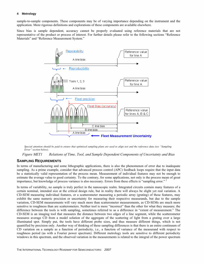
CRITICAL METROLOGY CONSIDERATIONS PRECISION AND UNCERTAINTY When comparing measurements with numbers in the roadmap, there are several important considerations to keep in mind. The validity of the comparison is strongly dependent upon how well those comparisons are made. The conventional interpretation of the ITRS precision1 has been to be purely the single tool 3σ reproducibility. After closer examination however2 3 it seems that the term “precision” is probably best thought of in broader terms as “uncertainty,” i.e. the error in measurement, colloquially known as the “error bar.” As follows from Figure MET1, measurement error is a complex function of time (reproducibility), tool (tool-to-tool matching) and sample (sample-to-sample bias variation). The measurement uncertainty is thus defined by total bias variation with measurement-to-measurement, tool-to-tool, and
1 For example, refer to SEMI E89-0999 “Guide for Measurement System Capability Analysis.”
THE INTERNATIONAL TECHNOLOGY ROADMAP FOR SEMICONDUCTORS: 2007
4 Metrology
sample-to-sample components. These components may be of varying importance depending on the instrument and the application. More rigorous definitions and explorations of these components are available elsewhere.
Since bias is sample dependent, accuracy cannot be properly evaluated using reference materials that are not representative of the product or process of interest. For further details please refer to the following sections “Reference Materials” and “Reference Measurement System.”
Fleet Measurement UncertaintyFleet Measurement UncertaintyFleet Measurement UncertaintyFleet Measurement Uncertainty
Special attention should be paid to ensure that optimized sampling plans are used to align test and the reference data (see “Sampling Error” section below).
Figure MET1 Relations of Time, Tool, and Sample Dependent Components of Uncertainty and Bias
SAMPLING REQUIREMENTS In terms of manufacturing and some lithographic applications, there is also the phenomenon of error due to inadequate sampling. As a prime example, consider that advanced process control (APC) feedback loops require that the input data be a statistically valid representation of the process mean. Measurement of individual features may not be enough to estimate the average value to good certainty. To the contrary, for some applications, not only is the process mean of great importance, but knowledge of process variance is also necessary. Errors from these effects is “sampling error.” 2
In terms of variability, no sample is truly perfect in the nanoscopic realm. Integrated circuits contain many features of a certain nominal, intended size at the critical design rule, but in reality there will always be slight yet real variation. A CD-SEM measuring individual features, or a scatterometer measuring a periodic array (grating) of these features, may exhibit the same numeric precision or uncertainty for measuring their respective measurands, but due to the sample variation, CD-SEM measurements will vary much more than scatterometer measurements, as CD-SEMs are much more sensitive to roughness than are scatterometers. Neither tool is more “incorrect” than the other for what they measure; the difference between the tools is with sampling, sometimes referred to as a difference in “extent of measurement.” The CD-SEM is an imaging tool that measures the distance between two edges of a line segment, while the scatterometer measures average CD from a model solution of the aggregate of the scattering of light from a grating over a large illuminated spot. Simply put, the tools have different probe sizes, and thus measure different things, which is not quantified by precision only. Another way of thinking of these sampling differences is that there is an entire continuum of CD variation on a sample as a function of periodicity, i.e., a function of variance of the measurand with respect to roughness period (as with a Fourier power spectrum). Different metrology tools are sensitive to different periodicity windows in this spectrum, and the observed variation in the measurements is related to the integral of the power spectrum
THE INTERNATIONAL TECHNOLOGY ROADMAP FOR SEMICONDUCTORS: 2007
Metrology 5
in each tool’s window of sensitivity. A scatterometer is more sensitive on very large periodicities with good estimation of average CD and little sensitivity to small periodicities, and a CD-SEM is more sensitive to smaller periodicities and localized variation. Note however, that with a larger sampling plan, a CD-SEM, averaging over a larger data set, can mimic the region of the scatterometer. Multiple Feature Measurement (MFM) applications are now available on CD-SEMs, allowing larger images to be analyzed and multiple CDs reported, improving confidence in the process mean while retaining sensitivity to real process variation and gaining sensitivity to larger roughness periodicities and linewidth variation. 4
When executing APC schemes, different techniques can yield different results due to differences in error in estimation of process mean. If sampling is not adequate, more variation is seen in the measurements (i.e., more “sampling noise”) and APC may be less successful. How to quantify the success of a tool with a given sampling scheme will be a topic of further future exploration. The answer will be highly dependent on the application in question. It will be very important to understand the needs of the application, such as the measurement objective (correlation/calibration, SPC, process assessment), how much variation is expected, and how important is knowledge of the variation and/or average value of the process. Further discussions of these considerations can be found elsewhere.
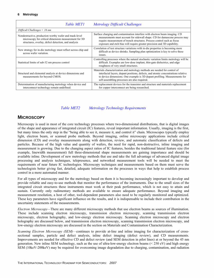
DIFFICULT CHALLENGES Many short-term metrology challenges listed below will continue beyond the 16 nm technology generation. Metrology needs after 2016 will be affected by unknown new materials and processes. Thus, it is difficult to identify all future metrology needs. Shrinking feature sizes, tighter control of device electrical parameters, such as threshold voltage and leakage current, and new interconnect technology such as 3D interconnect will provide the main challenges for physical metrology methods. To achieve desired device scaling, metrology tools must be capable of measurement of properties on atomic distances. Table MET1 presents the ten major challenges for metrology.
Table MET1 Metrology Difficult Challenges
Difficult Challenges ≥ 16 nm Summary of Issues Factory level and company wide metrology integration for real-
time in situ, integrated, and inline metrology tools; continued development of robust sensors and process controllers; and data management that allows integration of add-on sensors.
Standards for process controllers and data management must be agreed upon. Conversion of massive quantities of raw data to information useful for enhancing the yield of a semiconductor manufacturing process. Better sensors must be developed for trench etch end point, and ion species/energy/dosage (current).
Starting materials metrology and manufacturing metrology are impacted by the introduction of new substrates such as SOI. Impurity detection (especially particles) at levels of interest for starting materials and reduced edge exclusion for metrology tools. CD, film thickness, and defect detection are impacted by thin SOI optical properties and charging by electron and ion beams.
Existing capabilities will not meet Roadmap specifications. Very small particles must be detected and properly sized. Capability for SOI wafers needs enhancement. Challenges come from the extra optical reflection in SOI and the surface quality.
Control of new process technology such as Dual Patterning Lithography, complicated 3D structures such as capacitors and contacts for memory, and 3D Interconnect are not ready for their rapid introduction.
Overlay measurements for Dual Patterning have tighter control requirements. Overlay defines CD. 3D Interconnect comprises a number of different approaches. New process control needs are not yet established. For example, 3D (CD and depth) measurements will be required for trench structures including capacitors, devices, and contacts.
Measurement of complex material stacks and interfacial properties including physical and electrical properties.
Reference materials and standard measurement methodology for new high-κ gate and capacitor dielectrics with engineered thin films and interface layers as well as interconnect barrier and low-κ dielectric layers, and other process needs. Optical measurement of gate and capacitor dielectric averages over too large an area and needs to characterize interfacial layers. Carrier mobility characterization will be needed for stacks with strained silicon and SOI substrates, or for measurement of barrier layers. Metal gate work function characterization is another pressing need.
Measurement test structures and reference materials.
The area available for test structures is being reduced especially in the scribe lines. Measurements on test structures located in scribe lines may not correlate with in-die performance. Overlay and other test structures are sensitive to process variation, and test structure design must be improved to ensure correlation between measurements in the scribe line and on chip properties. Standards institutions need rapid access to state of the art development and manufacturing capability to fabricate relevant reference materials.
THE INTERNATIONAL TECHNOLOGY ROADMAP FOR SEMICONDUCTORS: 2007
6 Metrology
Table MET1 Metrology Difficult Challenges
Difficult Challenges < 16 nm
Nondestructive, production worthy wafer and mask-level microscopy for critical dimension measurement for 3D structures, overlay, defect detection, and analysis
Surface charging and contamination interfere with electron beam imaging. CD measurements must account for sidewall shape. CD for damascene process may require measurement of trench structures. Process control such as focus exposure and etch bias will require greater precision and 3D capability.
New strategy for in-die metrology must reflect across chip and across wafer variation.
Correlation of test structure variations with in-die properties is becoming more difficult as device shrinks. Sampling plan optimization is key to solve these issues.
Statistical limits of sub-32 nm process control Controlling processes where the natural stochastic variation limits metrology will be
difficult. Examples are low-dose implant, thin-gate dielectrics, and edge roughness of very small structures.
Structural and elemental analysis at device dimensions and measurements for beyond CMOS.
Materials characterization and metrology methods are needed for control of interfacial layers, dopant positions, defects, and atomic concentrations relative to device dimensions. One example is 3D dopant profiling. Measurements for self-assembling processes are also required.
Determination of manufacturing metrology when device and interconnect technology remain undefined.
The replacement devices for the transistor and structure and materials replacement for copper interconnect are being researched.
Table MET2 Metrology Technology Requirements
MICROSCOPY Microscopy is used in most of the core technology processes where two-dimensional distributions, that is digital images of the shape and appearance of integrated circuit (IC) features, reveal important information. Usually, imaging is the first, but many times the only step in the “being able to see it, measure it, and control it” chain. Microscopes typically employ light, electron beam, or scanned probe methods. Beyond imaging, online microscopy applications include critical dimension (CD) and overlay measurements along with detection, review, and automatic classification of defects and particles. Because of the high value and quantity of wafers, the need for rapid, non-destructive, inline imaging and measurement is growing. Due to the changing aspect ratios of IC features, besides the traditional lateral feature size (for example, linewidth measurement) full three-dimensional shape measurements are gaining importance and should be available inline. Development of new metrology methods that use and take the full advantage of advanced digital image processing and analysis techniques, telepresence, and networked measurement tools will be needed to meet the requirements of near future IC technologies. Microscopy techniques and measurements based on them must serve the technologists better giving fast, detailed, adequate information on the processes in ways that help to establish process control in a more automated manner.
For all types of microscopy and for the metrology based on them it is becoming increasingly important to develop and provide reliable and easy-to-use methods that monitor the performance of the instruments. Due to the small sizes of the integrated circuit structures these instruments must work at their peak performance, which is not easy to attain and sustain. Currently only rudimentary methods are available to ensure adequate performance. Beyond imaging and measurement resolution, a host of other, tool-dependent parameters also need to be regularly monitored and optimized. These key parameters have significant influence on the results, and it is indispensable to include their contribution in the uncertainty statements of the measurements.
Electron Microscopy—There are many different microscopy methods that use electron beams as sources of illumination. These include scanning electron microscopy, transmission electron microscopy, scanning transmission electron microscopy, electron holography, and low-energy electron microscopy. Scanning electron microscopy and electron holography are discussed below, and transmission electron microscopy, scanning transmission electron microscopy, and low-energy electron microscopy are discussed in the section on Materials and Contamination Characterization.
Scanning Electron Microscopy (SEM)—continues to provide at-line and inline imaging for characterization of cross-sectional samples, particle and defect analysis, inline defect imaging (defect review), and CD measurements. Improvements are needed for effective CD and defect review (and SEM detection in pilot lines) at or beyond the 45 nm generation. New inline SEM technology, such as the use of ultra-low-energy electron beams (< 250 eV) and high energy SEM (10keV-200keV) may be required for overcoming image degradation due to charging, contamination, and radiation
THE INTERNATIONAL TECHNOLOGY ROADMAP FOR SEMICONDUCTORS: 2007

Metrology 7
damage of the sample surface, while maintaining adequate resolution. Improving the resolution of the SEM by the reduction of spherical aberration leads to an unacceptably small depth of field and SEM imaging with several focus steps and/or use of algorithms that take the beam shape into account might be needed. Aberration correction lens technology has migrated from transmission electron microscopy to SEM providing a significant increase in capability. Other non-traditional SEM imaging techniques such as the implementation of nano-tips, and electron holography need to be developed, if they can prove to be production-worthy methodologies. A new alternative path could be high-pressure or environmental microscopy, which opens the possibility for higher accelerating voltage high-resolution imaging and metrology. Binary and phase-shifting chromium-on-quartz optical photomasks have been successfully investigated with this mode of high-resolution scanning electron microscopy. It has been found that the gaseous sample environment minimizes sample charging and contamination. This methodology also holds good potentials for the inspection, imaging, and metrology of wafers.
Data analysis methods that adhere to the physics of the measurement and do use all information collected were demonstrated to be better than arbitrary methods.5 Measured and modeled image and fast and accurate comparative techniques are likely to gain importance in SEM dimensional metrology. A better understanding of the relationship between the physical object and the waveform analyzed by the instrument is expected to improve CD measurement. Sample damage, which arises from direct ionization damage of the sample and deposition of charge in gate structures, may set fundamental limits to the utility of all microscopies relying on charged particle beams.
Determination of the real 3D shape for sub-90 nm contacts/vias, transistor gates, interconnect lines, or damascene trenches will require continuing advances in existing microscopy and sample preparation methods. Fully automated Cross-sectioning by FIB and semi-automated lift-out for imaging in a TEM or a STEM has been successfully demonstrated.
He Ion Microscopy (HIM)—has been proposed as a means of overcoming the issues associated with the spread in effect probe size associated with the interaction of finely focused electron beams and the sample. Potential applications of this technology include CD, defect review, and nanotechnology. Sub-1nm resolution by HIM has been achieved, but sample interaction questions are as yet unanswered.
Scanning Probe Microscopy (SPM)—may be used to calibrate CD-SEM measurements. Stylus microscopes, such as the atomic force microscope (AFM), offer 3D measurements that are insensitive to the material scanned. Flexing of the stylus degrades measurements, when the probe is too slender. The stylus shape and aspect ratio must, therefore, be appropriate for the probe material used and the forces encountered. High stiffness probe materials, such as short carbon nano-tubes, may alleviate this problem.
Far-field Optical Microscopy—is limited by the wavelength of light. Deep ultra-violet sources and near-field microscopy are being developed to overcome these limitations. Improved software allowing automatic classification of defects is needed. Optical microscopes will continue to have application in the inspection of large features, such as solder bump arrays for multi-chip modules.
For defect detection—each technology has limitations. A defect is defined as any physical, electrical, or parametric deviation capable of affecting yield. Existing SEMs and SPMs are considered too slow for the efficient detection of defects too small for optical microscopes. High-speed scanning has been demonstrated with arrayed SPMs, (that might be faster than SEMs) but issues associated with stylus lifetime, uniformity, characterization, and wear need to be addressed. This technology should be pursued both by expanding the size of the array and in developing additional operational modes. Arrayed micro-column SEMs have been proposed as a method of improving SEM throughput and operation of a single micro-SEM has been demonstrated. Research is needed into the limits of electrostatic and magnetic lens designs.
LITHOGRAPHY METROLOGY
Lithography metrology continues to be challenged by rapid advancement of patterning technology. New materials in all process areas add to the challenges faced by Lithography metrology. A proper control of the variation in transistor gate length starts with mask metrology. Although the overall features on a mask are four times larger than as printed, phase shift and optical proximity correction features are roughly half the size of the printed structures. Indeed, larger values for mask error factor (MEF) might require a tighter process control at mask level, too; hence, a more accurate and precise metrology has to be developed. Mask metrology includes measurements that determine that the phase of the light correctly prints. Both on-wafer measurement of critical dimension and overlay are also becoming more challenging. CD control for transistor gate length continues to be a critical part of manufacturing ICs with increasing clock speeds. The metrology needs for process control and dispositioning of product continue to drive improvements in measurement uncertainty. Acceleration of research and development activities for CD and overlay are essential if we are to provide
THE INTERNATIONAL TECHNOLOGY ROADMAP FOR SEMICONDUCTORS: 2007
8 Metrology
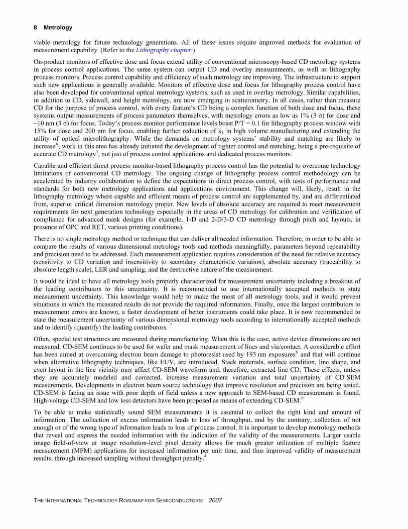
viable metrology for future technology generations. All of these issues require improved methods for evaluation of measurement capability. (Refer to the Lithography chapter.)
On-product monitors of effective dose and focus extend utility of conventional microscopy-based CD metrology systems in process control applications. The same system can output CD and overlay measurements, as well as lithography process monitors. Process control capability and efficiency of such metrology are improving. The infrastructure to support such new applications is generally available. Monitors of effective dose and focus for lithography process control have also been developed for conventional optical metrology systems, such as used in overlay metrology. Similar capabilities, in addition to CD, sidewall, and height metrology, are now emerging in scatterometry. In all cases, rather than measure CD for the purpose of process control, with every feature’s CD being a complex function of both dose and focus, these systems output measurements of process parameters themselves, with metrology errors as low as 1% (3 σ) for dose and ~10 nm (3 σ) for focus. Today’s process monitor performance levels boast P/T = 0.1 for lithography process window with 15% for dose and 200 nm for focus, enabling further reduction of k1 in high volume manufacturing and extending the utility of optical microlithography. While the demands on metrology systems’ stability and matching are likely to increase6, work in this area has already initiated the development of tighter control and matching, being a pre-requisite of accurate CD metrology3, not just of process control applications and dedicated process monitors.
Capable and efficient direct process monitor-based lithography process control has the potential to overcome technology limitations of conventional CD metrology. The ongoing change of lithography process control methodology can be accelerated by industry collaboration to define the expectations in direct process control, with tests of performance and standards for both new metrology applications and applications environment. This change will, likely, result in the lithography metrology where capable and efficient means of process control are supplemented by, and are differentiated from, superior critical dimension metrology proper. New levels of absolute accuracy are required to meet measurement requirements for next generation technology especially in the areas of CD metrology for calibration and verification of compliance for advanced mask designs (for example, 1-D and 2-D/3-D CD metrology through pitch and layouts, in presence of OPC and RET, various printing conditions).
There is no single metrology method or technique that can deliver all needed information. Therefore, in order to be able to compare the results of various dimensional metrology tools and methods meaningfully, parameters beyond repeatability and precision need to be addressed. Each measurement application requires consideration of the need for relative accuracy (sensitivity to CD variation and insensitivity to secondary characteristic variation), absolute accuracy (traceability to absolute length scale), LER and sampling, and the destructive nature of the measurement.
It would be ideal to have all metrology tools properly characterized for measurement uncertainty including a breakout of the leading contributors to this uncertainty. It is recommended to use internationally accepted methods to state measurement uncertainty. This knowledge would help to make the most of all metrology tools, and it would prevent situations in which the measured results do not provide the required information. Finally, once the largest contributors to measurement errors are known, a faster development of better instruments could take place. It is now recommended to state the measurement uncertainty of various dimensional metrology tools according to internationally accepted methods and to identify (quantify) the leading contributors. 7
Often, special test structures are measured during manufacturing. When this is the case, active device dimensions are not measured. CD-SEM continues to be used for wafer and mask measurement of lines and via/contact. A considerable effort has been aimed at overcoming electron beam damage to photoresist used by 193 nm exposures8 and that will continue when alternative lithography techniques, like EUV, are introduced. Stack materials, surface condition, line shape, and even layout in the line vicinity may affect CD-SEM waveform and, therefore, extracted line CD. These effects, unless they are accurately modeled and corrected, increase measurement variation and total uncertainty of CD-SEM measurements. Developments in electron beam source technology that improve resolution and precision are being tested. CD-SEM is facing an issue with poor depth of field unless a new approach to SEM-based CD measurement is found. High-voltage CD-SEM and low loss detectors have been proposed as means of extending CD-SEM.9
To be able to make statistically sound SEM measurements it is essential to collect the right kind and amount of information. The collection of excess information leads to loss of throughput, and by the contrary, collection of not enough or of the wrong type of information leads to loss of process control. It is important to develop metrology methods that reveal and express the needed information with the indication of the validity of the measurements. Larger usable image field-of-view at image resolution-level pixel density allows for much greater utilization of multiple feature measurement (MFM) applications for increased information per unit time, and thus improved validity of measurement results, through increased sampling without throughput penalty.4
THE INTERNATIONAL TECHNOLOGY ROADMAP FOR SEMICONDUCTORS: 2007
Metrology 9
For CD-SEMs, Design-Based Metrology (DBM) applications, which include automatic recipe setup from design information, allow for practical use of SEMs for large-scale verification of design intent, through the collection of feature 2D contour shape information and comparison to GDS files. DBM applications are becoming very important for development and verification of lithographic optical proximity corrections (OPC), as the number of measurements for successfully developing OPC is expected to grow exponentially with technology generation. Also, DBM applications for Double Patterning are being explored. This is a major role where metrology interfaces with the Design for Manufacturing (DFM) community.10 Also, collecting and applying CD information from reticle measurements for comparison to wafer CD measurements is an important application in some cases, and would be most efficient if done through contours.
However, much work remains to be done in defining contour error source testing methodologies, contour reference metrology, and SEM modeling for contours11 12 13. Contour fidelity is a prevailing challenge and an area where improvements in the state of the art could yield value to the industry. Gaps or missing segments in contours can occur for reasons related to both the sample and metrology tool. Major contributors are weak signal and breaks along edges parallel to the (fast) scan axis and contrast variation along the contour, which could be due to underlying variations in the structure (e.g., changes in sidewall angle or reentrance) or instrumental artifacts, such as edge proximity effects in an scanning electron microscope (SEM). In some cases, breaks in the contour are inherent when referencing one level to another (e.g., poly over active). This subject of contour integrity is closely related to the accuracy of contour extraction. Contour extraction algorithms employ 2-D image processing and thus function differently than conventional single-measurand critical dimension (CD) extraction algorithms, which are applied to individual line scans. There are known significant differences specifically with regard to edge detection and the inherent degree of signal averaging. Sampling can also have a large impact, as averaging as few as five contours can significantly improve precision and, due to averaging out local roughness effects in discrete features, also improve agreement between extracted contours and simulation.
Attention must also be paid to the requirements for registration between the SEM contours and the design for successful OPC. Models must be able to compensate for rotational and lateral offsets between the SEM contour and the design, as well as for potential field distortions. This relates somewhat to the question of metrology accuracy versus production accuracy. The extent to which it is acceptable to remove metrology errors when matching contours to the design is not agreed upon. For example, a uniform magnification error removed by stretching the contour could be less problematic than non-linearity across the SEM field of view.
Another area in which useful improvements could be made in contour metrology accuracy lies in the statistical sophistication of the contour extraction and modeling software, for example, the inclusion of a 95 % confidence interval for the extracted contour. It should be noted that the final metrics in measuring contours should be compatible with the same conventional linewidth metrics used in this roadmap.
Scatterometry has moved into manufacturing, and does provide line shape metrology. Scatterometry refers to both single wavelength—multi angle optical scattering and to multi-wavelength—single angle methods. Recent advances have resulted in the ability to determine CD and line shape without the aid of a library of simulated results. Scatterometry has already been shown to provide a tighter distribution of key transistor electrical properties when used in an advanced process control mode. The next step is the development of scatterometry for contact and via structures. Scatterometry models assume uniform optical property of line and background materials. Surface anomalies and non-uniform dopant distribution may affect scatterometry results. Therefore, scatterometry models need calibration and periodic verification. Lithography and etch microloading effects may noticeably affect line CD. Since scatterometry makes measurements on special test structures, other CD metrology techniques (such as SEM, AFM, or TEM) need to be employed to establish correlation between CD of the scatterometry structure and CDs of the circuit. Scatterometry needs to be capable of measuring smaller test structures while improving measurement precision. The increasing usage of double patterning may create some issues in measurement of double-patterned features, as many more parameters must be measured and controlled, potentially including two statistically distinct CD, sidewall, roughness, and pitch (overlay) populations. In some schemes, an ARC may prevent the UV light from penetrating deeper layers.
New CD measurement methods have been proposed, and it seems likely the first opportunity for them to move into manufacturing is at the 22 nm DRAM half pitch. The 32 nm half pitch is already well into the development stage and beta equipment is available for all process areas. The new potential solutions include the He ion microscope (discussed in the microscopy section) and small angle x-ray scattering (CD-SAXS). Using transmission measurements and a grating structure, CD-SAXS has shown the ability to measure average CD, sidewall roughness, and CD variation from an individual line in a grating structure.
The use of “feed forward” control concepts must be extended to lithography metrology taking data at least from resist and mask measurements and controlling subsequent processing, such as etch, to improve product performance. “Feed back”
THE INTERNATIONAL TECHNOLOGY ROADMAP FOR SEMICONDUCTORS: 2007
10 Metrology
controlling strategy is required as well to set properly process parameter setup from a huge amount of previously collected data. The use of overlay measurement equipment for CD control has also been reported. This method is based on the fact that the change in line width also affects the length of the photoresist lines that can then be measured using the optical microscope of the overlay system. A special test structure with arrays of line and arrays of spaces is required.
CD-AFM measurements can be used to verify line shape and calibrating CD or contour measurements. New probe tip technology and 3-D tiltable cantilever is required if CD-AFM is to be applied to dense line measurement below 50 nm. Focus–Exposure correlation studies (especially for contact/via) can be using all of the above methods as well as by the dual column FIB (SEM plus Focused Ion Beam) where there is an immediate correlation with line shape. Electron holography has been proposed as a long term CD measurement technology.
LINE ROUGHNESS Line edge roughness (LER) is an important part of lithography process control. Line width roughness (LWR) is an important part of etch process control. The Lithography Roadmap provides metrics for both LER and LWR. In 2001, LWR requirements were listed as LER. LWR was included in the 2001 ITRS because it was correlated to an increase in transistor leakage current but not to changes in drive current.14 LER and LWR are determined per the SEMI standard definition.15 It is important to note that the precision requirements for LER are several years ahead of those required for CD as indicated below. CD-SEM and lithography process simulation systems have software that determines LER, but not all systems yet adhere to the new SEMI standard for LER measurement.
LER/LWR is evaluated by two methods: spectral analysis and measurement of LER/LWR amplitude/degree (generally, 3 σ of residuals from average position or average CD). Fourier spectrum of LER/LWR is becoming popular in R&D; however, 3 σ is still the most useful index for practical in-line metrology. In evaluating LER/LWR, length of the inspected edge, L, and sampling interval of edge-detection, Δy, are the most important measurement parameters because 3 σ strongly depends upon these values.
The recommended LER/LWR metric is thus defined as the 3σ of residuals measured along 2- µ m-long line for the present; however, transistor performance could be more sensitive against in-gate roughness in the future. In that case, a new index for in-gate roughness (such as high-frequency LWR) should be additionally defined. To evaluate LWR-caused gate-CD variation separately, low-frequency LWR index should also be defined.
Another important factor in measurement of LWR/LER on imaging tools is edge detection noise. This noise has the effect of adding a positive bias to any roughness measurement. This is shown by the equation LWRmeas
2 = LWRactual2 + σε2
where LWRmeas is the measured value, LWRactual is the actual roughness of the target, and σε is the noise term, defined as the reproducibility of locating an edge along one single sampling point. The size of σε has been measured to be on the order of 2.5 nm, which means that at future technology generations this measurement artifact could mask the actual roughness to be measured. A methodology has been demonstrated to remove this noise term, leading to an unbiased estimation of the roughness. Use of this is deemed very important to ensuring accuracy of roughness measurement in the future, and should be a key ingredient in allowing for intercomparison of data across the litho-metrology community.16 It should be noted that LWR metrology becomes more challenging when the resolution of the metrology tool becomes close to the LWR requirement. At the 22 nm node the LWR required is 1.3 nm. Current CD-SEM equipment has comparable resolution performance.
MEASUREMENT UNCERTAINTY Critical dimension measurement capability does not meet precision requirements that comprehend measurement variation from individual tool reproducibility, tool-to-tool matching and sample-to-sample measurement bias variation. Precision is defined by SEMI as a multiple of reproducibility. Reproducibility includes repeatability, variation from reloading the wafer, and long-term drift. In practice, reproducibility is determined by repeated measurements on the same sample and target over an extended period of time. Although the precision requirements for CD measurement in the ITRS have always included the effects of line shape and materials variation, repeated measurements on the same sample would never detect measurement uncertainty related to sample-to-sample bias variation. Therefore, with the current methodology the uncertainty of measurement associated with variation of line shape, material, layout, or any other parameters will not be included in the precision. Typically, reference materials for CD process control are specially selected optimum or “golden” wafers from each process level. Thus, industry practice is to determine measurement precision as a reproducibility of the measurement for each process level. The measurement bias is not detected. This approach misses measurement bias variation component of measurement uncertainty. In light of this, a metric, total measurement uncertainty (TMU) can be used. 17, 18. The TMU is determined using a technology representative set of samples that accounts for variations in measurement bias associated with each process level. This idea can be extended to use with a production fleet of tools through another metric Fleet Matching Precision (FMP).19 These metrics assume accuracy for all
THE INTERNATIONAL TECHNOLOGY ROADMAP FOR SEMICONDUCTORS: 2007
Metrology 11
tools, and that a fleet of tools behave as well as a single tool would be required. It should be noted that other metrics for accuracy and matching are also available.
Calibration of inline CD metrology equipment requires careful implementation of the calibration measurement equipment referred to as reference metrology. For example, laboratory based TEM or CD-AFM must have precision that matches or exceeds inline CD and have to be frequently calibrated. Reference materials used during manufacturing must be representative to the actual process level and structure and reflect the pertinent process variations to be evaluated by the tool under test. Reports of this approach already exist.20
CD measurement has been extended to line shape control. Tilt beam CD-SEM, comparison of line scan intensity variation versus line scans from a golden wafer, scatterometry, CD-AFM, dual beam (electron and gallium ion beam systems) and triple beam (electron, Gallium ion beam and Argon ion beam systems) have all been applied to line shape measurement. Sidewall angle has been proposed as the key process variable. Already, photoresist lines have shapes that are not well described by a single planar description of the sidewall. Line edge and line width roughness along a line, vertical line edge roughness, and rounded top shapes are important considerations in process control. As mentioned above, precision values change with each process level. This adds to the difficulty in determination of etch bias (the difference in CD before and after etch). Electrical CD measurements provide a monitoring of gate and interconnect line width, but only after the point where reworking the wafers is no longer possible and does not allow a real-time correction of process parameter. Electric CD measurements are limited in their applicability to conducting samples.
Mask metrology is moving beyond the present optical technology. Binary and phase-shifting chromium on quartz optical photomasks have been successfully investigated with high-pressure/environmental scanning electron microscopy. Environmental SEM instrumentation equipped with high-resolution, high-signal, field emission technology in conjunction with large chamber and sample transfer capabilities are in use in the semiconductor industry for mask CD. The high-pressure SEM methodology employs a gaseous environment to help to compensate for the charge build-up that occurs under irradiation with the electron beam. Although potentially very desirable for the charge neutralization, this methodology has not been seriously employed in photomask or wafer metrology until now. This is a new application of this technology to this area, and it shows great promise in the inspection, imaging, and metrology of photomasks in a charge-free operational mode. This methodology also holds the potential of similar implications for wafer metrology. For accurate metrology, high-pressure SEM methodology also affords a path that minimizes, if not eliminates, the need for charge modeling.
Lithography metrology consists not only of overlay and CD metrology, but also includes the process control and characterization of materials needed for lithography process, especially photoresists, phase shifters, and antireflective coatings (ARCs). As these lithography materials become more complex, the materials characterization associated with them also increases in difficulty. Additionally, most non-lithography materials used in the wafer fabrication process (gate oxides, metals, low-κ dielectrics, SOI substrates) enter the lithography process indirectly, since their optical properties affect the reflection of light at a given wavelength. Even a small variation in process conditions for a layer not normally considered critical to the lithography process (such as the thickness of the buried oxide in SOI wafers) can change the dimensions or shapes of the printed feature, if this process change affected the optical response of the layer.
As a minimum, the complex refractive index (refractive index n and extinction coefficient κ) of all layers needs to be known at the lithography wavelength. Literature data for such properties are usually not available or obsolete and not reliable (derived from obsolete reflectance measurements on materials of unknown quality followed by Kramers-Kronig transform). In ideal cases, n and κ can be measured inline using spectroscopic ellipsometry at the exposure wavelength. Especially below 193 nm, such measurements are very difficult and usually performed outside of the fab by engineering personnel. EUV optical properties can only be determined using specialized light sources (such as a synchrotron or a EUV source for a EUV litho tool). Therefore, materials composition is often used as a figure of merit, when direct measurement of the optical properties is not practical. But even two materials with the same composition can have different optical properties (take amorphous and crystalline Si as an example).
Additional complications in the determination of the optical properties of a material arise from surface roughness, interfacial layers, birefringence, or optical anisotropy (often seen in photoresists or other organic layers responding to stress), or depth-dependent composition. For some materials for a wafer fab, it is impossible to determine the optical properties of such material, since the inverse problem of fitting the optical constants from the ellipsometric angles is underdetermined. Therefore, physical materials characterization must accompany the determination of optical properties, since physical characteristics, materials properties, and optical constants are all inter-related.
Overlay measurements are challenged by phase shift masks (PSM) and optical proximity correction (OPC) masks, and the use of different exposure tools and/or techniques for different process layers will compound the difficulty. Future overlay
THE INTERNATIONAL TECHNOLOGY ROADMAP FOR SEMICONDUCTORS: 2007
12 Metrology
metrology requirements, along with problems caused by low contrast levels, will drive the development of new optical or SEM methods along with scanning probe microscopy (SPM). The need for new target structures has been suggested as a means of overcoming the issues associated with phase shift mask and optical proximity mask alignment errors not detectable with traditional targets. Overlay for on-chip interconnect will continue to be challenging. The use of chemical mechanical polishing for planarization degrades target structures. Thus as requirements for tighter overlay control are introduced, the line edge of overlay targets in interconnect are roughened. The low-κ materials used as insulators will continue to make overlay more difficult especially as porous low κ move into manufacturing.
The dramatic tightening of the overlay budget up to 20% [or 25%] of the device half-pitch, required for advanced applications in DRAM and NVM, calls for a faster introduction of alternative measuring solutions, like high-voltage SEM and scatterometry techniques, which are still far from being mature enough today, and may require breakthroughs also in metrology integration.
The introduction of EUV lithography requires further development in the area of EUV mask metrology and EUV Aerial Image Measurements Systems (EUV AIMS).
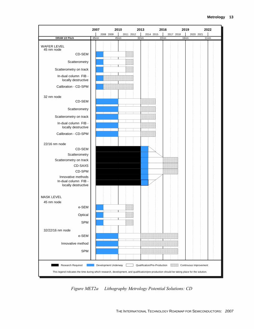
The Lithography Metrology Requirements Tables are divided into wafer and mask requirements Tables MET3, and MET4a and MET4b, respectively. The mask metrology requirements in Tables MET4a and MET4b are further divided into the needs for each type of exposure technology: optical, EUV, and electron projection.
EXPLANATION OF UNCERTAINTY IN TABLES MET3 AND MET4 The preceding concepts are summarized by the following consideration for the precision of patterning metrology: the definition for precision critically depends on the application. Given the application and the metrology instrument, a sampling plan needs to be defined. The precision specification needs to be interpreted in light of application, instrument, and sampling plan. The application defines the accuracy, single tool precision, and matching requirements. In some applications, the relative accuracy and single tool precision are paramount. In some applications, tool matching and single tool precision are paramount. In some applications, a single measurement event is not sufficient to provide the needed measurement; rather the average of multiple measurement events constitute the critical measurement episode; in this case the precision should be interpreted as the uncertainty requirement of the average. The precision numbers in the tables are changed to uncertainty numbers. The relation to precision and uncertainty (σ) is given in formula (1).
LLUL6
TP
−σ⋅
= (1)
2other
2S
2M
2p σ+σ+σ+σ=σ (2)
Uncertainty (σ) contains the following components: σP (Precision), σM (Matching), σS (Sampling) and σother (inaccuracy and other effects). We assume normal distributions where each factor is independent and only random variations occur.
Table MET3 Lithography Metrology (Wafer) Technology Requirements
Table MET4a Lithography Metrology (Mask) Technology Requirements: Optical
Table MET4b Lithography Metrology (Mask) Technology Requirements: EUV
THE INTERNATIONAL TECHNOLOGY ROADMAP FOR SEMICONDUCTORS: 2007
Metrology 13
DRAM 1/2 Pitch
Development Underway Qualification/Pre-Production Continuous ImprovementResearch Required
This legend indicates the time during which research, development, and qualification/pre-production should be taking place for the solution.
2008 2009 2011 2012 2014 2015 2017 2018 2020 202165nm
2007
45nm
2010
22nm
2016
16nm
2019
11nm
2022
32nm
2013
MASK LEVEL
32/22/16 nm nodee-SEM
Innovative method
SPM
45 nm nodee-SEM
Optical
SPM
WAFER LEVEL
22/16 nm nodeCD-SEM
ScatterometryScatterometry on track
CD-SAXS
CD-SPMInnovative methods
In-dual column FIB -locally destructive
32 nm nodeCD-SEM
Scatterometry
Scatterometry on track
In-dual column FIB -locally destructive
Calibration - CD-SPM
45 nm nodeCD-SEM
Scatterometry
Scatterometry on track
In-dual column FIB -locally destructive
Calibration - CD-SPM
Figure MET2a Lithography Metrology Potential Solutions: CD
THE INTERNATIONAL TECHNOLOGY ROADMAP FOR SEMICONDUCTORS: 2007
14 Metrology
DRAM 1/2 Pitch
Development Underway Qualification/Pre-Production Continuous ImprovementResearch Required
This legend indicates the time during which research, development, and qualification/pre-production should be taking place for the solution.
65nm
20072008 2009
45nm
20102011 2012
32nm
20132014 2015
22nm
20162017 2018
16nm
20192020 2021
11nm
2022
22/16 nm node
Scattering based optical
SEM
Optical
32 nm node
Scattering based optical
SEM
Optical
45 nm node
Scattering based optical
SEM
Optical
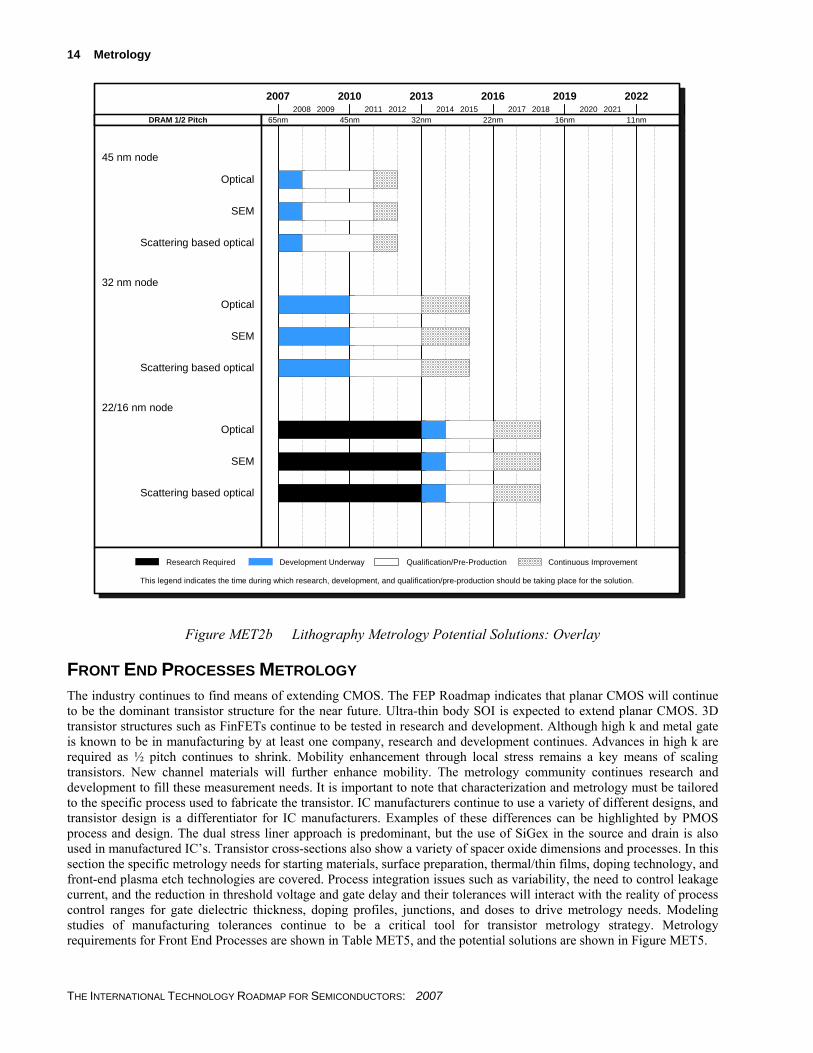
Figure MET2b Lithography Metrology Potential Solutions: Overlay
FRONT END PROCESSES METROLOGY The industry continues to find means of extending CMOS. The FEP Roadmap indicates that planar CMOS will continue to be the dominant transistor structure for the near future. Ultra-thin body SOI is expected to extend planar CMOS. 3D transistor structures such as FinFETs continue to be tested in research and development. Although high k and metal gate is known to be in manufacturing by at least one company, research and development continues. Advances in high k are required as ½ pitch continues to shrink. Mobility enhancement through local stress remains a key means of scaling transistors. New channel materials will further enhance mobility. The metrology community continues research and development to fill these measurement needs. It is important to note that characterization and metrology must be tailored to the specific process used to fabricate the transistor. IC manufacturers continue to use a variety of different designs, and transistor design is a differentiator for IC manufacturers. Examples of these differences can be highlighted by PMOS process and design. The dual stress liner approach is predominant, but the use of SiGex in the source and drain is also used in manufactured IC’s. Transistor cross-sections also show a variety of spacer oxide dimensions and processes. In this section the specific metrology needs for starting materials, surface preparation, thermal/thin films, doping technology, and front-end plasma etch technologies are covered. Process integration issues such as variability, the need to control leakage current, and the reduction in threshold voltage and gate delay and their tolerances will interact with the reality of process control ranges for gate dielectric thickness, doping profiles, junctions, and doses to drive metrology needs. Modeling studies of manufacturing tolerances continue to be a critical tool for transistor metrology strategy. Metrology requirements for Front End Processes are shown in Table MET5, and the potential solutions are shown in Figure MET5.
THE INTERNATIONAL TECHNOLOGY ROADMAP FOR SEMICONDUCTORS: 2007
Metrology 15
Table MET5 Front End Processes Metrology Technology Requirements
The impact of shrinking dimension on FEP metrology is already at the point where research devices and materials exhibit materials properties associated with nano-science. For example the properties of nanowire like shapes such as a FIN in a FINFET are quantum confined in two dimensions.
Starting materials—Many of the metrology challenges related to starting materials involve the emerging class of layered materials such as SOI and strained silicon on SOI. The trend toward thinner layers, along with multiple layer interfaces, poses a challenge to most material metrology techniques.
Areas of concern include the following: • Bulk Ni and Cu measurement on p+, silicon on insulator (SOI), strained silicon (SSi), and strained silicon on
insulator (SSOI) wafers • Measurement of 109–1010 cm-3 Fe (and other bulk metals) in the top Si of thin SOI wafers • Thickness and uniformity of very thin SOI layers (<20 nm) • Defectivity of thin layers (e.g., threading dislocations, “HF defects”) • Particle detection (<100 nm) on layered surfaces
Small particle detection continues to be of concern for the future. Note that due to metrology capability issues the silicon starting materials particle requirements below 65 nm size will not require sub-65 nm metrology but will model the critical number of sub-65 nm particles based upon the number of particles detected at 65 nm size. More information can be found in the Starting Materials section of the Front End Processes chapter.
Silicon-On-Insulator (SOI) is entering the mainstream of IC device applications, and this is expected to grow further along the Roadmap. An expectation has been that the materials specifications for polished silicon substrates would be transferred to SOI specifications. However, the underlying insulator structure in SOI negatively affects many of the metrology capabilities used for polished silicon substrates. Thus, there is some difficulty to measure and control SOI material properties at the level desired. The metrology community has addressed this but some issues remain. For more details on these metrology challenges see the FEP chapter on Starting Materials.
Surface preparation—In situ sensors for particles, chemical composition, and possibly for trace metallics are being introduced to some wet chemical cleaning tools. Particle detection is covered in the Yield Enhancement chapter. Particle/defect and metallic/organic contamination analyses are covered in the Materials Characterization Section of the Metrology chapter. The role of impurities in high-κ gate dielectrics, and therefore their measurement requirements, is a future research topic. For the present the required impurity levels are projected to be the same as for silicon oxynitride gate dielectrics, but the measurement of those impurities is not clear.
Thermal/thin films—While Hf-related oxides were first used for manufactured logic devices in 2008, the roadmap indicates that increasingly higher dielectric constants will be needed in the future. Thus, alternative oxides will need to be developed and metrology challenges are expected for these new developments. The high κ gate stack contains several significant challenges that require further research and development. Measurement of nitrogen concentration in high-κ dielectrics is difficult. The films used to adjust the gate work function are very thin and nanoscale roughness may prove to be of the same dimensions as film thickness making it impossible to use some traditional measurement methods. Materials characterization of annealed gate stacks challenges all methods including ultra-high resolution TEM. In addition, new DRAM structures that use mixed high-κ dielectrics, and even ultra-thin layers of stacked high-κ dielectrics, will challenge metrology development.
Metrology research and development is required for advancement of new channel materials including germanium and III-Vs. Measurement needs are driven by the challenges associated with producing defect free crystal structures due to lattice mismatch with the silicon substrate. Measurement needs include observation and quantification of defect states in the band gap and dislocation densities. Many measurements require blanket films. At this time, correlation of measurements of blanket films with channel layers in transistors will require use of cross-sections which may not be representative of the total transistor structure.
Strained Si processes—Carrier mobility enhancement through process induced local stress continues to be a critical means of improving drive current and thus transistor performance. Typically, NMOS transistors are given tensile stress by applying Si3N4 stress liner film over the gate electrode. One of several different processes is used for PMOS transistors. In the replacement source-drain process, PMOS transistor channels are given compressive stress by the replacement of the
THE INTERNATIONAL TECHNOLOGY ROADMAP FOR SEMICONDUCTORS: 2007
16 Metrology
silicon in the source and drain with selectively grown SiGe. The second means is through a compressive Si3N4 stress liner. Shallow trench isolation (STI) is another source of compressive stress in the channel. Here, the pattern layout of active area, gate electrode, and contact hole must be carefully designed and the processes should be tightly controlled. A combination of techniques and selection of Si crystal orientation in the channel have also been proposed. New processes in the development phase require stress characterization and metrology. These include a Si:C (heavily carbon-doped silicon) replacement source-drain process which is under consideration for NMOS. SiC would induce tensile stress in the NMOS channel region.
In order to accelerate design of the pattern layout and process conditions, a non-destructive direct measurement of the stress in the nano-sized area is desired. The importance of Finite Element Simulations of stress and resulting electrical properties has already been shown to be a key aspect of process development and metrology. Accurate stress metrology can help calibrate these simulations. As new processes are introduced with new technology generations, the challenge renews itself. Further complicating the challenge is the timing of the potential transition to alternate channels and the introduction of FINFETS or wrap around gates. This year line items for local stress/strain measurements for both of off-line and in-line metrology have been introduced to the metrology technology requirements Table MET5. It is expected that test pad would be used for in-line stress/strain measurement and its size is estimated as around 100 µm × 100 µm.
Review of Stress Measurement Methods is shown in Figure MET3. This review shows a clear contrast in spatial localization capability between off-line methods such as convergent beam electron diffraction (CBED) and potential in-line methods from the stand points of off-line destructive metrology and in-line non-destructive metrology.
Figure MET3 Review of Stress/Strain Measurement Methods
FERAM—Although the thickness of the dielectric films are 100 to 200 nm, optical models for inline film thickness measurement of the metal oxides must be developed when a new materials set is used. The main metrology need is for fatigue testing of the capacitor structures at 1016 read write cycles and above.
Cross-sections of memory devices illustrate the challenges associated with fabrication and process control for complex 3D memory structures created in a sequence of at least two patterning levels (pattern over pattern). Many measurement needs are not covered by simplified test structures. The impact of overlay errors is illustrated in Figure MET4. Cross-sectional metrology needs such as improved dimensional precision are a key requirement for memory and other 3D structures.
THE INTERNATIONAL TECHNOLOGY ROADMAP FOR SEMICONDUCTORS: 2007
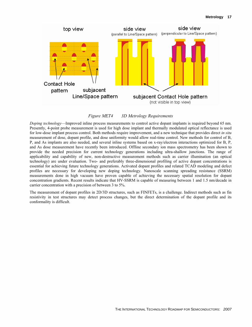
Metrology 17
Figure MET4 3D Metrology Requirements Doping technology—Improved inline process measurements to control active dopant implants is required beyond 65 nm. Presently, 4-point probe measurement is used for high dose implant and thermally modulated optical reflectance is used for low-dose implant process control. Both methods require improvement, and a new technique that provides direct in situ measurement of dose, dopant profile, and dose uniformity would allow real-time control. New methods for control of B, P, and As implants are also needed, and several inline systems based on x-ray/electron interactions optimized for B, P, and As dose measurement have recently been introduced. Offline secondary ion mass spectrometry has been shown to provide the needed precision for current technology generations including ultra-shallow junctions. The range of applicability and capability of new, non-destructive measurement methods such as carrier illumination (an optical technology) are under evaluation. Two- and preferably three-dimensional profiling of active dopant concentrations is essential for achieving future technology generations. Activated dopant profiles and related TCAD modeling and defect profiles are necessary for developing new doping technology. Nanoscale scanning spreading resistance (SSRM) measurements done in high vacuum have proven capable of achieving the necessary spatial resolution for dopant concentration gradients. Recent results indicate that HV-SSRM is capable of measuring between 1 and 1.5 nm/decade in carrier concentration with a precision of between 3 to 5%.
The measurement of dopant profiles in 2D/3D structures, such as FINFETs, is a challenge. Indirect methods such as fin resistivity in test structures may detect process changes, but the direct determination of the dopant profile and its conformality is difficult.
THE INTERNATIONAL TECHNOLOGY ROADMAP FOR SEMICONDUCTORS: 2007
18 Metrology
DRAM 1/2 Pitch
Development Underway Qualification/Pre-Production Continuous ImprovementResearch Required
This legend indicates the time during which research, development, and qualification/pre-production should be taking place for the solution.
65nm
20072008 2009
45nm
20102011 2012
32nm
20132014 2015
22nm
20162017 2018
16nm
20192020 2021
11nm
2022
22/16 nm node
Compositional metrology
Stress metrology(see Figure MET3)
Optical and x-rayfilm thickness
32 nm node
Compositional metrology
Stress metrology(see Figure MET3)
Optical and x-rayfilm thickness
45 nm node
Compositional metrology
Stress metrology(see Figure MET3)
Optical and x-rayfilm thickness
Figure MET5 FEP Metrology Potential Solutions
INTERCONNECT METROLOGY New processes and structures continue to drive metrology research and development. Porous low κ is moving into manufacturing, and 3D Interconnect is being used in a great variety of implementations. Copper contact structures were announced at key technical symposia. All areas of metrology including materials characterization, in-line measurements, and advanced equipment and process control are used for interconnect research, development, and manufacturing. Reliability of new processes such as copper contacts is largely unknown. As it has been in the past, reliability testing is a critical part of evaluating new processes.
Interconnects, including all of the IC structures necessary to connect from silicon to the boards and boxes of the outside world, have become a potential performance roadblock for the continuation of the semiconductor industry on the Moore’s Law curve. This roadblock has components in both technology and cost. It has technology components spanning the necessary transition from aluminum/SiO2 to Cu/low κ, as well as in transitions to more radical approaches to interconnects beyond the metal/dielectric system. It has cost components in the anticipated high cost of fabrication of alternatives to the incumbent metal dielectric interconnect system for global interconnects using current technology. Among the potential roadblocks and cost issues inherent in the switch from aluminum/SiO2 to Cu-low κ are the significant challenges for new metrology for process development, manufacturing validation, and process control. For example, in Cu-low κ it is desired to produce minimal thickness barriers between Cu and dielectrics. This has resulted in a need for metrology for detailed characterization of extremely thin layers and “zero thickness” interfaces without the
THE INTERNATIONAL TECHNOLOGY ROADMAP FOR SEMICONDUCTORS: 2007
Metrology 19
undesirable effects occurring during destructive sample preparation. One of the most challenging issues facing interconnect metrology is the lack of measurement capability for sidewalls of trenches and vias. The anticipation of moves to radical interconnect options, such as optical interconnects, has led to new metrology issues such as the need to profile optical properties of very narrow waveguides, and to be able to identify extremely small optical defects in such waveguide materials. Some of the needed metrology problems have been solved with creative applications and advances of existing techniques, and some new techniques have been developed. However, some problems have been identified as particularly difficult, and possibly not having solutions within the confines of currently envisioned metrology techniques.
Interconnect needs for metrology, as noted above, include continuing evolutionary advances in existing metrology techniques, as well as the increasing need for novel metrology approaches for more radical interconnect structures. The following sections will first describe some of the needs and status of existing metrology techniques for current Interconnects, and will then address some of the needed advances for future directions in interconnect. In addition to the on-chip interconnect, a new approach to chip to chip interconnect known as 3D interconnect has emerged. This section will also discuss metrology for 3D Interconnect. Refer to the Interconnect chapter.
3D INTERCONNECT ISSUES AND METROLOGY Through silicon vias (TSV) provide a means connecting die directly without using wires. TSV structures have high aspect ratios making them difficult to etch and fill despite their relatively large size. The first metrology challenge starts when the wafers are bonded. The alignment must be checked through the wafer, and bonding integrity determined. Infrared microscopy is capable of measuring overlay target structures through the silicon since silicon is transparent in the IR. Scanning acoustic microscopy (SAM) is also capable of measuring subsurface features. SAM has been successfully applied to observation of voids and defects between bonded wafers. X-ray microscopy is another method capable of “seeing” through silicon structures. All these methods require advances in spatial resolution especially as TSV diameter shrinks. A number of other measurement needs are receiving considerable attention including stress and adhesion (delamination) measurements. A list of TSV measurement needs includes:
• TSV Depth and Profile through multiple layers • Alignment of chips for stacking – wafer level integration • Bond strength • Defects in bonding • Damage to metal layers • Defects in vias between wafers • Through Si via is a high aspect ratio CD issue • Wafer thickness and TTV after thinning • Defects after thinning including wafer edge
CU-LOW κ METALLIZATION ISSUES AND METROLOGY NEEDS CU METALLIZATION ISSUES Copper metallization has been used for several generations. The latest advance in copper metallization is the use of copper contacts to the transistor replacing tungsten. With each shrink, the challenges of filling trenches and vias must be faced again. Among the most important of these is the need for precise control of electrochemical deposition baths, and identification of very low-level impurities that may cause resistivity increases in electrochemically deposited copper. We now know that the reliability of copper metal interconnects is degraded by the effects of electro and stress migration, and that the primary degradation modes are associated with surface diffusion of Cu along the interfaces between the Cu and dielectrics and barriers. Voids in metal lines and vias that occur during processing have also been identified as significant yield loss initiators. Voiding problems can show up after deposition/CMP/anneal, or from agglomeration of micro-voids due to electro or stress migration. Another significant problem relating to voids is a need to be able to identify relatively small, isolated voids in large fields of patterned Cu conductors. These isolated voids often do not show up as yield loss, but can be an incipient cause of later reliability failures. These voids may be on the surface of the conductors, but are often buried within the conductor pattern or in vias. Additional issues with Cu metallization arise from the use of thin barriers to isolate the Cu from underlying dielectrics. These thin barriers raise significant needs for measurement capabilities of ultra thin layers, interface properties, and defects and materials structure on sidewalls in very narrow channels.
THE INTERNATIONAL TECHNOLOGY ROADMAP FOR SEMICONDUCTORS: 2007
20 Metrology
The problems noted above have all been found to be important for Cu metallization at 90 nm and above. As the industry moves below 90 nm, it is expected that these issues will still be present, but that additional issues will arise. While we do not know all of the new issues that will arise, several problems associated with our inability to extrapolate current techniques to the very small geometries, or increasing importance of currently acceptable limitations of metrology for future technology generations, are already clear. Among these future needs for Cu metallization metrology is the increasing importance of metrology for ultra thin layers—especially barriers on sidewalls. This need requires not only the ability to establish physical properties and structure of these layers with thicknesses <2 nm, but also to identify and characterize defects in the films. An additional problem area that is currently not extensively studied, but that is expected to become increasingly important at smaller conductor geometries is the interface between the Cu and the barrier or dielectric that it interfaces. As the Cu conductors become smaller, it is expected that interface scattering will cause significant increases in resistivity of very narrow lines.
CU METALLIZATION METROLOGY Copper electroplating systems need quantitative determination of the additives, byproducts, and inorganic contents in the bath to maintain the desired properties in the electroplated copper film. Process monitoring requires in situ measurements of additives, byproducts, and inorganic content that result from bath aging. A mass spectrometry based method of real-time sampling of bath contents provides a new potential solution. Cyclic voltammetric stripping (CVS) is widely used to measure the combined effect of the additives and byproducts on the plating quality. Liquid Chromatography can be used to quantitative measure individual components or compounds that are electrochemically inactive and volumetric analysis using titration methods can be used for the monitoring of inorganics. Barrier layer metrology needs include measurement of thickness, spatial uniformity, defects, and adhesion. Inline measurement for 3D structures continues to be a major gap. Measurement of materials on sidewall of low κ trenches is made even more difficult by the roughness along the sidewall. There is some concern about the application of statistical process control to very thin barrier layers. Interconnect technical requirements indicate that barrier layers for future technology will be <5 nm thick. The 2001 ITRS specified a process window of 20% total thickness variation. The measurement precision (6σ) for a 6 nm film must be ≤0.12 nm, which is beyond current capabilities. It may be possible to use existing metrology capability to determine the presence or absence of these very thin films without using traditional SPC. Presently, a number of measurement methods are capable of measuring a barrier layer under seed copper when the films are horizontal. These methods include acoustic methods, X-ray reflectivity, and X-ray fluorescence. Some of these methods can be used on patterned wafers. At-line determination of the crystallographic texture (grain orientation) has been demonstrated using grazing X-ray diffraction. Detection of voids in copper lines is most useful after CMP and anneal processes. A metric for copper void content has been proposed in the Interconnect Roadmap and in line metrology for copper voids is the subject of much development. However, these efforts are focusing on the detection of voids only and not on the statistical sampling needed for process control. Many of the methods are based on detection of changes in the total volume of the copper lines. The typical across-chip variation in the thickness of copper lines will mask the amount of voiding that these methods can observe. Interconnect structures, which involve many layers of widely varying thickness made from a variety of material types, pose the most severe challenge to rapid, spatially resolved (for product wafers) multi-layer thickness measurements. Inline measurement of crystallographic phase and crystallographic texture (grain orientation) of copper/barrier films is now possible using X-ray diffraction based methods. This technology is under evaluation for process monitoring, and the connection to electrical properties and process yield is being investigated. Post CMP processes for interconnect structures require measurement of dishing and erosion in the copper lines. Current optical and acoustic techniques have been explored, but need to address the statistical sampling requirements for the accurate detection of dishing and erosion on a manufacturing environment. Other areas of metrological concern with the new materials and architectures include in-film moisture content, film stoichiometry, mechanical strength/rigidity, local stress (versus wafer stress), and line resistivity (versus bulk resistivity). In addition, calibration techniques and standards need to be developed in parallel with metrology. Advances in measurement technology have enabled in situ control of Chemical Mechanical Polishing (CMP) and determination of the thickness of buried barrier films on horizontal surfaces. The pose size distribution of porous low κ can be measured using small angle X-ray scattering or ellipsometric porisimetry. Although voids can be detected in fields of copper lines, most methods determine a change in the volume of copper lines. Thus, process induced changes such as those that occur across the wafer from CMP can mask the presence of voids. Metrology for inline control of bath chemistry is being implemented. Some measurements remain elusive. For example, measurement of barrier and seed copper film thickness on sidewalls is not yet possible. Recently crystallographic texture measurements on sidewalls have been reported. Adhesion strength
THE INTERNATIONAL TECHNOLOGY ROADMAP FOR SEMICONDUCTORS: 2007
Metrology 21
measurements are still done using destructive methods. End point detection for etch must be developed for new etch stop materials for porous low κ. Detection of killer pores and voids is not yet possible. The accelerated reduction in feature size makes development of metrology for high aspect ratio features a greater challenge for on-chip interconnect development and manufacture. Critical dimension measurements are also a key enabler for development of interconnect processes. CD metrology must be extended to very high aspect ratio structures made from porous dielectric materials and requires 3D information for trench and via/contact sidewalls. These measurements will be further complicated by the underlying multi film complexity. Development of interconnect tools, processes, and pilot line fabrication all require detailed characterization of patterned and unpatterned films. Currently, many of the inline measurements for interconnect structures are made on simplified structures or monitor wafers and are often destructive. Small feature sizes including ultra-thin barrier layers will continue to stretch current capabilities. Interconnect metrology development will continue to be challenged by the need to provide physical measurements that correlate to electrical performance, yield, and reliability. More efficient and cost-effective manufacturing metrology requires measurement on patterned wafers. Metrology requirements for Interconnect are shown in Table MET6 and the potential solutions are shown in Figure MET6 below. The new measurement requirements for void detection in copper lines and killer pores in low κ appear to be difficult or impossible to meet. The need is to have a rapid, inline observation of very small number of voids/larger pores. The main challenge is the requirement that the information be a statistically significant determination at the percentage specified in Table MET6.
Table MET6 Interconnect Metrology Technology Requirements
LOW κ DIELECTRICS ISSUES AND METROLOGY NEEDS LOW κ DIELECTRIC ISSUES The move from SiO2 to other dielectrics to provide lower dielectric constants in interconnect structures is proving as much, if not more, of a challenge to the semiconductor industry than the move from Al metallization to Cu. A significant part of the difficulties has come from the fact that low κ materials available thus far have significantly different physical and mechanical properties than the prior SiO2. Among the primary differences are significantly different mechanical properties, and the presence of pores in the material. The lower mechanical strength has resulted in a new set of issues stemming from problems resulting from materials and processes used in back end manufacturing showing up as problems at assembly and packaging. A significant part of the problem is that there is no convenient and competent metrology tools and methodology to qualify materials at the back end process stage for assembly and packaging viability. A second major issue has been identified with characterization of porous materials. At the present time there are no metrology techniques and methodologies to identify anomalously large or significantly connected pores (so called “killer pores”) in otherwise smaller pored materials. There are also no available metrology techniques to characterize the materials on the sidewalls of low κ patterns for physical properties, chemical structure, and electrical performance. This capability needs to be able to identify and quantify very thin layers on these sidewalls related to physical layers and damage due to processes such as pore sealing and plasma etch. These features need to be quantifiable both on continuous sidewall surfaces and into pores on porous materials. The two issues noted above, along with the standard measurements associated with dielectrics, need to be addressed for not only today’s dielectrics, but also for those that will be used in the few nanometer generations of the not too distant future.
LOW-Κ METROLOGY Inline metrology for non-porous low-κ processes is accomplished using measurements of film thickness and post CMP flatness. In situ sensors are widely used to control CMP. Metrology continues to be a critical part of research and development of porous low-κ materials. The need for transition of some of the measurements used during process development into volume manufacturing is a topic of debate. Examples include pore size distribution measurement. Pore size distribution has been characterized off-line by small angle neutron scattering, positron annihilation, a combination of gas absorption and ellipsometry (ellipsometric poresimetry), and small angle X-ray scattering (SAXS). SAXS and ellipsometric poresimetry can be used next to (at-line) a manufacturing line. The need for moving these methods into the fab is under evaluation. Detection of large, “killer,” pores in patterned low κ has been highlighted as a critical need for manufacturing metrology by the Interconnect Roadmap.
High-frequency measurement of low-κ materials and test structures has been developed up to 40 GHz. This needs to be extended to ~100 GHz because 20 GHz clocks have rising and falling edges much above 40 GHz. As a result of extensive
THE INTERNATIONAL TECHNOLOGY ROADMAP FOR SEMICONDUCTORS: 2007
22 Metrology
evaluation, the interconnect community no longer considers this measurement a critical need in the near term. Low-κ materials seem to have constant dielectric functions over the frequency range of interest (from 1 GHz to 10 GHz).
Thinning of porous low κ during chemical mechanical polishing technology must be controlled, and available flatness metrology further developed to for patterned porous low-κ wafers. Stylus profilers and scanned probe (atomic force) microscopes can provide local and global flatness information, but the throughput of these methods must be improved. Standards organizations have developed (and continue to develop) flatness tests that provide the information required for statistical process control that is useful for lithographic processing.
Interconnect specific CD measurement procedures must be further developed for control of etch processes. Key gaps include the ability to validate post etch clean effectiveness, sidewall damage layer and properties. Rapid 3D imaging of trench and contact/via structures must provide profile shape including sidewall angle and bottom CD. This is beyond the capabilities of current inline CD-SEMs. Etch bias determination is difficult due to the lack of adequate precision for resist CD measurements. One potential solution is scatterometry, which provides information that is averaged over many lines with good precision for M1 levels, but this precision may degrade for higher metal levels. Furthermore, scatterometry must be extended to contact and via structures. Electrical test structures continue to be an important means of evaluating the R-C properties of patterned low-κ films.
Measurement of low-κ mechanical properties lead to a reduced number of candidate materials. This work needs to continue for new low-κ materials. Other gaps include measurement of stress in closely spaced trenches.
THE INTERNATIONAL TECHNOLOGY ROADMAP FOR SEMICONDUCTORS: 2007
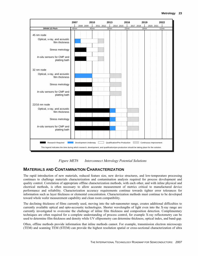
Metrology 23
DRAM 1/2 Pitch
Development Underway Qualification/Pre-Production Continuous ImprovementResearch Required
This legend indicates the time during which research, development, and qualification/pre-production should be taking place for the solution.
65nm
20072008 2009
45nm
20102011 2012
32nm
20132014 2015
22nm
20162017 2018
16nm
20192020 2021
11nm
2022
22/16 nm node
In-situ sensors for CMP andplatting bath
Stress metrology
Optical, x-ray, and acousticfilm thickness
32 nm node
In-situ sensors for CMP andplatting bath
Stress metrology
Optical, x-ray, and acousticfilm thickness
45 nm node
In-situ sensors for CMP andplatting bath
Stress metrology
Optical, x-ray, and acousticfilm thickness
Figure MET6 Interconnect Metrology Potential Solutions
MATERIALS AND CONTAMINATION CHARACTERIZATION The rapid introduction of new materials, reduced feature size, new device structures, and low-temperature processing continues to challenge materials characterization and contamination analysis required for process development and quality control. Correlation of appropriate offline characterization methods, with each other, and with inline physical and electrical methods, is often necessary to allow accurate measurement of metrics critical to manufactured device performance and reliability. Characterization accuracy requirements continue towards tighter error tolerances for information such as layer thickness or elemental concentration. Characterization methods must continue to be developed toward whole wafer measurement capability and clean room compatibility.
The declining thickness of films currently used, moving into the sub-nanometer range, creates additional difficulties to currently available optical and opto-accoustic technologies. Shorter wavelengths of light even into the X-ray range are currently investigated to overcome the challenge of inline film thickness and composition detection. Complimentary techniques are often required for a complete understanding of process control, for example X-ray reflectometry can be used to determine film thickness and density while UV ellipsometry can determine thickness, optical index, and band-gap.
Often, offline methods provide information that inline methods cannot. For example, transmission electron microscopy (TEM) and scanning TEM (STEM) can provide the highest resolution spatial or cross-sectional characterization of ultra
THE INTERNATIONAL TECHNOLOGY ROADMAP FOR SEMICONDUCTORS: 2007
24 Metrology
thin films and interfacial layers. STEM systems equipped with X-ray detection and electron energy loss spectroscopy (EELS) have provided new information about interface chemical bonding. High-performance secondary ion mass spectroscopy (SIMS), and its variant time-of-flight (TOF) SIMS, provide contamination analysis of surfaces and thin film stacks. Grazing incidence X-ray reflectivity (XRR) provides measurement of thin film thickness and density, while grazing incidence X-ray diffraction provides information about the crystalline texture of thin films. The importance of using diffuse scattering in addition to specular scattering during XRR seems to be critical to building interfacial models from XRR that can be compared to interfacial models from other methods such as TEM/STEM, SIMS, and ion backscattering. Field emission Auger electron spectroscopy (FE-AES) provides composition analysis of particulate contamination down to less than 20 nm in size. Offline characterization of physical properties such as void content and size in porous low-κ insulators, film adhesion, and mechanical properties, for example, is required for evaluation of new materials. Many of these tools are now available for full wafers up to 300 mm in diameter.
Continued development of TEM and STEM imaging capability is required. TEM/STEM methods require sample preparation methods that can result in metrology artifacts if care is not taken. Choice of detection angle for annular detectors employed in STEM instruments allows imaging contrast to vary from incoherent imaging sensitive to mass-thickness variations to coherent imaging sensitive to crystal orientation and strain. Several technologies are being applied to materials and process development for critical areas such as high and low κ. Electron energy loss spectroscopy (EELS) can achieve spatial resolution of atomic columns for oriented crystalline samples, however, choice of incident beam convergence angle and detector collection angles (especially for high convergence angles afforded by modern aberration corrected instruments). With this greatly improved spatial resolution, EELS can be used to characterize interfacial regions such as that between high κ and silicon substrate. STEM with Annular Dark Field imaging and EELS are becoming more routine in manufacturing support labs, however spatial resolution in regular practice is often limited by real device samples where amorphous and disordered interfaces increase probe interaction volumes beyond those afforded by channeling along atomic columns in perfect crystals. Further routine site-specific sample preparation conducted by focused ion beam generally produces samples in the 100 nm thickness range. For certain applications such as litho cross section metrology of photoresist and gate side wall angle measurements, this is sufficient21. More challenging applications require a thickness of below 50 nm for optimal spatial resolution in imaging and analysis. Great advances have been made using in situ argon beam thinning of samples22. Then, automated sample preparation of sub-100 nm thick samples becomes feasible. Advances in image reconstruction software have also improved image resolution and thus interfacial imaging. Several improvements in TEM/STEM technology are now commercially available including lens aberration correction and monochromators for the electron beam. Recent breakthroughs in aberration corrected scanning TEM look very promising and reveal details such as single misplaced atoms in a junction. Further, via combined application of aberration correctors and monochomators and high-brightness electron sources, improved resolution may be achieved at reduced incident beam acceleration potentials allowing TEM measurements below knock-on damage threshold energies that have plagued high resolution characterization of fragile materials including carbon nanotubes and graphene. All of these improved resolutions in TEM/STEM require improved sample preparation; thinner samples and reduced surface-damage layers are required. Though at present it’s generally considered time-prohibitive, electron tomography, producing 3D models of device structures, may play an increasingly important role in metrology. Tomography has less stringent sample preparation conditions as surface damage regions may be removed from reconstructions and thicker samples are generally desired to allow a larger reconstructed volume.
Prototype microcalorimeter energy dispersive spectrometers (EDS) and superconducting tunnel junction techniques have X-ray energy resolution capable of separating peaks that overlap and cannot be resolved with current generation lithium-drifted-silicon EDS detectors. Such new X-ray detectors will allow resolution of slight chemical shifts in X-ray peaks providing chemical information such as local bonding environments. These advances over traditional EDS and some wavelength dispersive spectrometers can enable particle and defect analysis on SEMs located in the clean room. Although beta site systems have been tested, unfortunately, these have not become widely available. These detectors can also be implemented in micro XRF systems, using either an electron beam or a micro focus X-ray beam as excitation source. XPS (X-ray photon electron spectroscopy) is now widely used as a means to determine thickness and composition of thin (up to 50 nm) films.
While these and other offline characterization tools provide critical information for implementing the Roadmap, there are still many challenges. Characterization of high-κ gate stacks is difficult due to the length-scales for which electrical properties are determined. For example chemical intermixing by reactions forming intermetallics or alloys may be easily confused with physical roughness at an interface, and characterization is difficult in these situations due to matrix-induced effects and overlapping signals. Characterization techniques which probe the local atom-atom interactions including electron energy loss spectroscopy, X-ray absorption near edge structure spectroscopies are often required. In addition, as device features continue to shrink and new non-planar MOS devices are developed, the applicability of characterizing
THE INTERNATIONAL TECHNOLOGY ROADMAP FOR SEMICONDUCTORS: 2007
Metrology 25
planar structures as representative of device features becomes more questionable. Furthermore, ongoing scaling makes the analysis of contamination in high aspect ratio structures even more difficult.
The introduction of new materials will raise new challenges in contamination analysis, such as happened with copper metallization where the very real possibility of cross contamination has led to the need to measure bulk copper contamination down to the order of 1010 atoms/cm3 and surface copper contamination even in the edge exclusion and bevel regions, all because of the high diffusivity properties of this deleterious metal. Device shrinks are also tending to lower the thermal budgets allowed for processing so that the behavior of metal contamination and how to reduce its negative effects are changing the characterization needs. For example, low-temperature processing is changing which surface contamination elements, and at what levels, need to be controlled and therefore measured. A key example is the role of surface calcium on very thin gate oxide integrity, and the difficult challenge of measuring this surface element at the 108 atoms/cm3 level. Traditional methods such as vapor phase decomposition ICP-MS can have day-to-day limitations at this level. In addition, low-temperature processing is changing how metal contamination gettering is achieved, challenging the way to characterize material properties to ensure proper gettering.
The 2007 Metrology Roadmap reported that a new approach to contamination control was being developed for inline measurement. Real-time sampling of wet chemical baths has been added to a mass spectrometry based detection system for measurement of trace contamination in the bath solutions. These systems do not appear to be widely available yet.
The accelerated use of strained silicon without SOI has resulted in new metrology and characterization requirements earlier than predicted in the 2003 Roadmap; these are currently under evaluation and development. Gate oxide metrology becomes even more complex if strained Si channel structures are used as the starting material instead of bulk Si or SOI wafers. Strained Si is either grown on thick relaxed SiGe buffer layers on bulk Si or on compliant substrates consisting of thin SiGe layers on SOI. In both cases, the metrology of the starting material is crucial with a large number of parameters to be controlled: 1) thickness and Ge profile of the SiGe buffer, 2) thickness of the strained Si channel, 3) roughness of the Si/SiGe interface and the Si surface, 4) magnitude and local variation of stress in the Si channel, 5) threading dislocation density in the Si channel (high sensitivity of the measurement is needed, since the desirable dislocation density is very low (at <103-104cm-2)), 6) density of other defects, such as twins, dislocation pile-ups, or misfit dislocations, particularly at the SiGe/Si channel interface, 7) distribution of dopants in channel and buffer (particularly after thermal annealing).
TEM is readily available to determine thicknesses and interface/surface roughness of strained silicon on a microscopic scale. Several methods employing TEM/STEM have been developed to measure and map strain distributions in strained-channel devices. It has been noted that thinning of a TEM sample may allow relaxation of some of the strain, and finite element modeling has been useful in understanding how strain may be relaxed during sample thinning, however strain measurement by TEM/STEM has had many successes. Both threading and misfit dislocations can be measured by TEM, but the limited sample size area if often a problem for required statistical analysis of dislocation densities. Atomic force microscopy determines the surface roughness of the Si channel. Optical microscopy has been successful for etch pit density (EPD) measurements to determine the density of threading dislocations intercepting the wafer surface. Clear prescriptions for EPD are needed to select the etch depth. The meaning of lines and points in the EPD optical images need to be explained. X-ray topography is another technique offering promise for defect detection. The Ge and dopant profiles can easily be measured with SIMS. A high sputtering rate is needed for thick SiGe buffers, while high depth resolution (possibly with a low-energy floating ion gun) enables the analysis of the thin Si channel and of the channel/buffer interface. Optical carrier excitation using a red photodiode directed at the sputtering crater has been used to avoid SIMS charging artifacts; this is particularly important for strained Si over SOI and for undoped layers.
Unique properties associated with strained silicon are being addressed with a variety of metrology methods. Stress is the force required to create lattice strain which affects the electronic band structure to provide mobility enhancement of electrons or holes. Raman spectroscopy can measure stress, while TEM and XRD measure strain. Raman spectrometry measures the energy of the Si-Si vibration in the Si channel which depends on changes in stress. However, the phonon deformation potential (describing the variation of the Si-Si phonon energy with stress) is not firmly established for thin Si channels. Such Raman measurements need to be performed using a UV laser to avoid penetration of the laser into the Si substrate. At 325 nm wavelength, the entire Raman signal stems from the thin Si channel, simplifying data analysis. For longer wavelengths, the Si-Si vibration in the SiGe buffer complicates the signal. The energy of the Si-Si vibration in SiGe depends on alloy composition and stress, which complicates the problem. Raman mapping yields the stress distribution across the wafer with a maximum resolution of about 0.5 µm, thus allowing prediction of transistor-to-transistor variations in mobility enhancement. It would be desirable to improve this resolution, possibly using solid or liquid immersion techniques. Micro-XRD is also applied to measure the stress in small structures, but currently the analysis spot is in the 5–10 micron range, making device analysis not yet feasible.
THE INTERNATIONAL TECHNOLOGY ROADMAP FOR SEMICONDUCTORS: 2007
26 Metrology
Analysis of ellipsometry data for strained Si channels is complicated, since the dielectric function of Si depends on the stress. This relationship (described by the piezo-optical or elasto-optical tensors) is qualitatively understood, but sufficiently accurate quantitative data for fitting ellipsometry data of strained Si channels is lacking. When only considering the UV portion of the ellipsometry spectra, there is some hope in the capability to determine the gate oxide thickness, at least for sufficiently smooth surfaces. For rougher surfaces, there is an additional source of error, since surface roughness enters the ellipsometry analysis in a similar fashion as the native or gate oxide. For accurate gate oxide metrology, the Si surface roughness should be an order of magnitude less than the gate oxide thickness. This is satisfied for bulk Si starting materials, but may cause concerns for measurements on strained Si channels. Confinement effects in the thin Si channel are not yet an issue in the visible and UV portions of the ellipsometry spectra. In principle, ellipsometry should not only be able to determine the Si channel thickness, but also the Ge content of the SiGe buffer underneath. In practice, however, the Ge content determined from ellipsometry data is much too low, possibly due to ignoring the strain effects on the Si dielectric function. On pseudomorphic Si/SiGe heterostructures, ellipsometry is much more successful.
X-ray reflectivity is an attractive alternative to spectroscopic ellipsometry to determine strained Si channel thickness since the refractive index for X-rays is very close to 1 and does not depend on the stress. For Si channel thicknesses of the order of 10–20 nm, a clear series of interference fringes (sometimes accompanied by an additional large-angle peak of unknown origin) is obtained. However, determining the Si channel thickness using commercial software fitting packages does not always yield the correct value (in comparison to TEM). Possibly, this is related to surface roughness that is more difficult to handle for X-ray reflectivity than for spectroscopic ellipsometry because of the smaller wavelength. Experimental concerns about X-ray instrument reliability and alignment are similar to that described for measurements on high-κ gate dielectrics. High-resolution triple-axis X-ray diffraction has been used successfully (using lab and synchrotron X-ray sources) to determine the vertical Si lattice constant in the channel, another measure for the stress in the structures. A number of microscopy methods are in the research and development phase. These include the point projection microscope (electron holography) and low-energy electron microscopy. Low-energy electron microscopy has been used to study surface science for several years. The application of this method to materials characterization and possibly to inline metrology needs to be studied. A discussion of these methods is provided in the Microscopy Section of the Metrology Roadmap.
One of the five long-term difficult challenges for metrology is structural and elemental analysis at device dimensions. Fulfilling this need will require developing materials characterization methods that provide maps of elemental or chemical distributions at an atomic scale in three dimensions. 3D Atom Probes and similar methods hold promise of providing atom-by-atom maps for small (50-150 nm diameter) needle shaped samples that may be prepared by FIB lift-out techniques. LEAP technology needs further method and data analysis development, and currently has difficulties in measuring non-conductive and heterogeneously-conductive structures with both conducting and non-conducting features. One challenge will be obtaining near 100% detection of each element during data acquisition. Electron tomography is a growing region of interest and is being pursued by both tilt-series and focal series methods in both STEM and TEM. Aberration corrected TEM currently shows promise in this area as smaller and more intense probes may allow increased resolution and signal to noise required for tomographic analysis.
THE INTERNATIONAL TECHNOLOGY ROADMAP FOR SEMICONDUCTORS: 2007
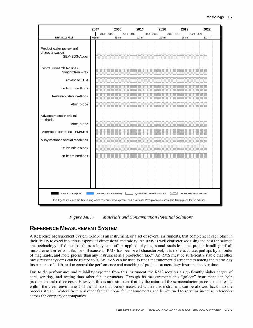
Metrology 27
DRAM 1/2 Pitch
Development Underway Qualification/Pre-Production Continuous ImprovementResearch Required
This legend indicates the time during which research, development, and qualification/pre-production should be taking place for the solution.
65nm
20072008 2009
45nm
20102011 2012
32nm
20132014 2015
22nm
20162017 2018
16nm
20192020 2021
11nm
2022
Advancements in criticalmethods
Ion beam methods
He ion microscopy
X-ray methods spatial resolution
Aberration corrected TEM/SEM
Atom probe
Central research facilities
Atom probe
New innovative methods
Ion beam methods
Advanced TEM
Synchrotron x-ray
Product wafer review andcharacterization
SEM-EDS-Auger
Figure MET7 Materials and Contamination Potential Solutions
REFERENCE MEASUREMENT SYSTEM A Reference Measurement System (RMS) is an instrument, or a set of several instruments, that complement each other in their ability to excel in various aspects of dimensional metrology. An RMS is well characterized using the best the science and technology of dimensional metrology can offer: applied physics, sound statistics, and proper handling of all measurement error contributions. Because an RMS has been well characterized, it is more accurate, perhaps by an order of magnitude, and more precise than any instrument in a production fab.23 An RMS must be sufficiently stable that other measurement systems can be related to it. An RMS can be used to track measurement discrepancies among the metrology instruments of a fab, and to control the performance and matching of production metrology instruments over time.
Due to the performance and reliability expected from this instrument, the RMS requires a significantly higher degree of care, scrutiny, and testing than other fab instruments. Through its measurements this “golden” instrument can help production and reduce costs. However, this is an instrument that, by the nature of the semiconductor process, must reside within the clean environment of the fab so that wafers measured within this instrument can be allowed back into the process stream. Wafers from any other fab can come for measurements and be returned to serve as in-house references across the company or companies.
THE INTERNATIONAL TECHNOLOGY ROADMAP FOR SEMICONDUCTORS: 2007
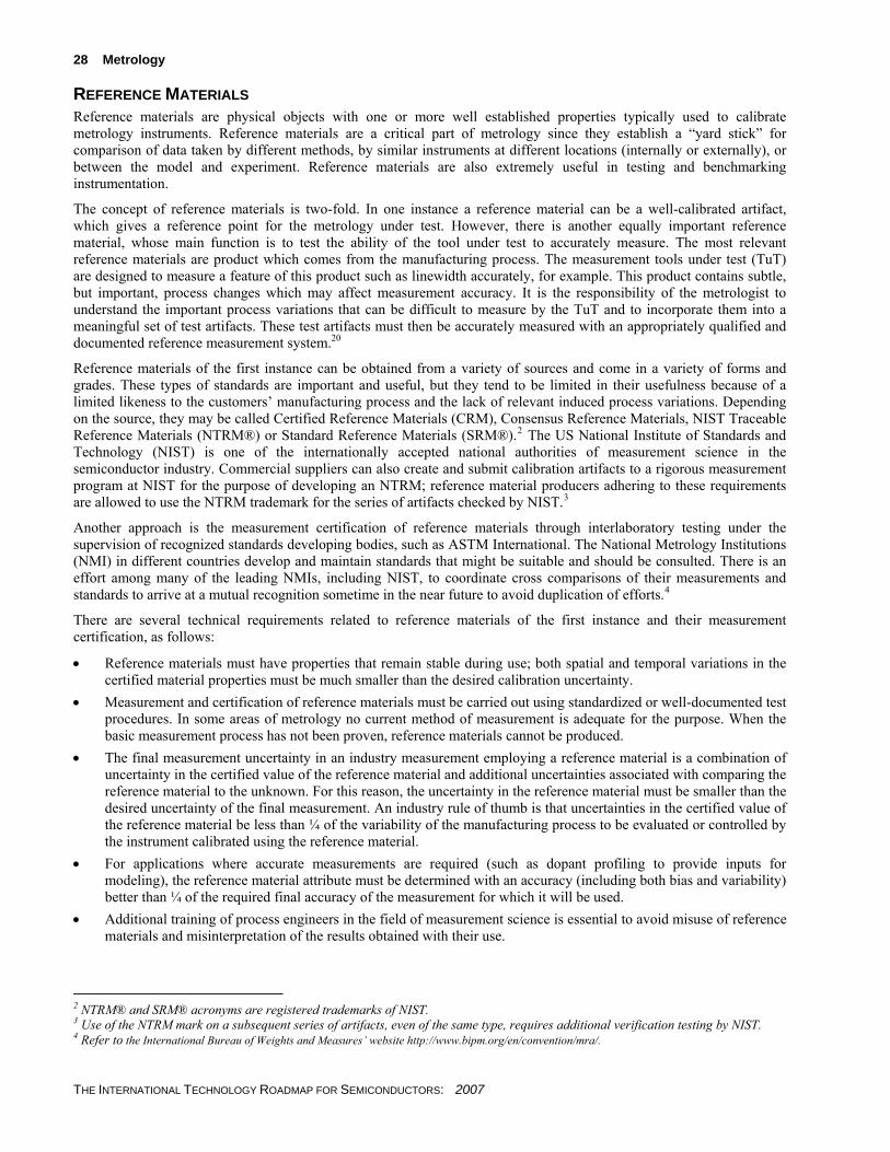
28 Metrology
REFERENCE MATERIALS Reference materials are physical objects with one or more well established properties typically used to calibrate
ce materials are a critical part of metrology since they establish a “yard stick” for
ference point for the metrology under test. However, there is another equally important reference
and useful, but they tend to be limited in their usefulness because of a
he National Metrology Institutions
operties must be much smaller than the desired calibration uncertainty.
ciated with comparing the
metrology instruments. Referencomparison of data taken by different methods, by similar instruments at different locations (internally or externally), or between the model and experiment. Reference materials are also extremely useful in testing and benchmarking instrumentation.
The concept of reference materials is two-fold. In one instance a reference material can be a well-calibrated artifact, which gives a rematerial, whose main function is to test the ability of the tool under test to accurately measure. The most relevant reference materials are product which comes from the manufacturing process. The measurement tools under test (TuT) are designed to measure a feature of this product such as linewidth accurately, for example. This product contains subtle, but important, process changes which may affect measurement accuracy. It is the responsibility of the metrologist to understand the important process variations that can be difficult to measure by the TuT and to incorporate them into a meaningful set of test artifacts. These test artifacts must then be accurately measured with an appropriately qualified and documented reference measurement system.20
Reference materials of the first instance can be obtained from a variety of sources and come in a variety of forms and grades. These types of standards are importantlimited likeness to the customers’ manufacturing process and the lack of relevant induced process variations. Depending on the source, they may be called Certified Reference Materials (CRM), Consensus Reference Materials, NIST Traceable Reference Materials (NTRM®) or Standard Reference Materials (SRM®).2 The US National Institute of Standards and Technology (NIST) is one of the internationally accepted national authorities of measurement science in the semiconductor industry. Commercial suppliers can also create and submit calibration artifacts to a rigorous measurement program at NIST for the purpose of developing an NTRM; reference material producers adhering to these requirements are allowed to use the NTRM trademark for the series of artifacts checked by NIST.3
Another approach is the measurement certification of reference materials through interlaboratory testing under the supervision of recognized standards developing bodies, such as ASTM International. T(NMI) in different countries develop and maintain standards that might be suitable and should be consulted. There is an effort among many of the leading NMIs, including NIST, to coordinate cross comparisons of their measurements and standards to arrive at a mutual recognition sometime in the near future to avoid duplication of efforts.4
There are several technical requirements related to reference materials of the first instance and their measurement certification, as follows:
• Reference materials must have properties that remain stable during use; both spatial and temporal variations in the certified material pr
• Measurement and certification of reference materials must be carried out using standardized or well-documented test procedures. In some areas of metrology no current method of measurement is adequate for the purpose. When the basic measurement process has not been proven, reference materials cannot be produced.
• The final measurement uncertainty in an industry measurement employing a reference material is a combination of uncertainty in the certified value of the reference material and additional uncertainties assoreference material to the unknown. For this reason, the uncertainty in the reference material must be smaller than the desired uncertainty of the final measurement. An industry rule of thumb is that uncertainties in the certified value of the reference material be less than ¼ of the variability of the manufacturing process to be evaluated or controlled by the instrument calibrated using the reference material.
• For applications where accurate measurements are required (such as dopant profiling to provide inputs for modeling), the reference material attribute must be determined with an accuracy (including both bias and variability) better than ¼ of the required final accuracy of the measurement for which it will be used.
• Additional training of process engineers in the field of measurement science is essential to avoid misuse of reference materials and misinterpretation of the results obtained with their use.
2 NTRM® and SRM® acronyms are registered trademarks of NIST. 3 Use of the NTRM mark on a subsequent series of artifacts, even of the same type, requires additional verification testing by NIST. 4 Refer to the International Bureau of Weights and Measures’ website http://www.bipm.org/en/convention/mra/.
THE INTERNATIONAL TECHNOLOGY ROADMAP FOR SEMICONDUCTORS: 2007
Metrology 29
• It is critically important to have suitable reference materials available when a measurement is first applied to a technology generation, especially during early materials and process equipment development. Each type of reference
rol (APC). The trend toward powerful spectrum of process
r systematic drift in ss behavior. Here, R2R control has been the dominant driver, in which
e sensors are used to identify common equipment
r multivariate control capabilities. While in situ real-time sensors in principle can drive run-to-run
ipment drifts, using feedback information to adjust process settings for the next wafer, and/or compensating for
material has its own set of difficult challenges, involving different combinations of the challenges described above.
INTEGRATED METROLOGY AND ADVANCED PROCESS CONTROL Metrology plays a key role enabling productivity gains made through advanced process contintegrated metrology—from offline to inline to in situ techniques—enables a richer, more control strategies. At this point, advances in APC have been driven primarily by successes in run-to-run (R2R) control and in fault detection and classification (FDC). The advances in integrated metrology and APC have been substantial though in some ways serendipitous. It is clear that: 1) APC has demonstrated major value to the industry, and has been adopted by most manufacturers; 2) APC capabilities and associated sensors and metrology to support APC are available today for key process areas such as CMP and lithography, but 3) a truly comprehensive APC manufacturing strategy is not yet reality, nor is a portfolio of sensors and metrology tools to support complete factory-wide deployment, particularly given the profound changes in materials, processes, and device structures expected for future technology generations. The benefits already realized from APC are driving the development of new sensor technologies and associated control software, which will allow factory-wide comprehensive solutions to be realized in the near future.
APC comprises two different thrusts as follows:
1) Course correction is aimed at adjustment of process parameters in order to compensate foequipment, incoming product variation, and proceinline metrology is employed for feedback or feed-forward control, either on a wafer-to-wafer or batch-to-batch basis to maintain product quality in the presence of process variations, and also to reduce non-product wafers. Real-time control, based on in situ and real-time sensors for during-process course correction, generally requires further development of more process-specific sensors with sufficient metrological precision.
2) Fault management is directed at rapid identification and response to equipment problems. The primary driver has been fault detection and classification (FDC), in which in situ and real-timfaults, suggest or initiate repair actions, and reduce product scrap. Additional benefit is envisioned as sensor and metrology data are combined with informatics approaches to enable more sophisticated classification of more subtle fault sources, along with fault prognosis and maintenance rescheduling consistent with overall tool and factory efficiency improvement. Building on the increasing confidence that R2R and FDC successes have provided, the challenges for these two APC components are to add real-time control to R2R control for course correction, and to expand FDC to broader fault management.
Inline metrology tools now underpin broad implementations of R2R control, involving both feedback and multi-step feed-forward univariate ocontrol, they have been primarily exploited for real-time fault detection, with a limited number of examples in real-time course correction (e.g., interferometric etch end-point control). The economic value of both run-to-run course correction and real-time fault detection have led to advances in equipment engineering capabilities (EEC),that is, broad integration of APC hardware, models and algorithms with factory-level information distribution, scheduling, and operations. Despite these advances, availability of comprehensive APC systems requires further R&D in sensors, control strategies, new applications, and improved user interfaces to these APC systems to reduce the barriers to understanding and acceptance of APC.
Since R2R is primarily based on inline metrology, it delivers value primarily by compensating for longer-term process and equincoming product variability (wafer-to-wafer, lot-to-lot, etc.) by using feed-forward information to adjust the subsequent process(es) experienced by the same wafer. FDC delivers value by determining the health of the tool or process through evaluation of in situ information (process, equipment, and wafer). This evaluation may occur in real-time, i.e., during processing, or as summary activity after processing has been completed. In the latter case, inline wafer metrology represents a driver for FDC as well as R2R control. The increased availability and standardization of R2R control and FDC and their associated interfaces will also lead to control strategies and solutions that incorporate both capabilities in a complementary fashion. R2R control and FDC will be integrated as follows: 1) at the data storage level, thereby supporting data sharing and data mining between application types; 2) at the user interface level, thereby reducing the APC learning curve and allowing APC to be represented as a single entity in the factory; 3), at the logic interaction level, whereby control rules will allow FDC results to impact R2R control operation and vice-versa to support complementary utilization of these capabilities, and 4) eventually, at the algorithm level, where FDC and R2R models and modeling
THE INTERNATIONAL TECHNOLOGY ROADMAP FOR SEMICONDUCTORS: 2007
30 Metrology
approaches would be integrated. Items 1) through 3) above will be critical to the realization of comprehensive factory-wide manufacturing strategies. The technology to support all of these items is incomplete. Other factors that will lead to factory-wide strategies include hierarchical control solutions, cascaded control between processes, and coordination of control with yield management applications. Another key APC enabler is the development of standards that define the interaction of the APC applications with each other and with outside agents, and ensure access to wafer, process and equipment data as necessary to support these applications.
APC will benefit from the move to integrated metrology, though a significant number of benefits from R2R control can be achieved with offline metrology. For example, with lithography overlay and CD control, integrated metrology will
metrology, which should be comparable to those for stand-alone
pensates for short-term, random process variability. In turn, this will enable a true
r development and demonstration as sufficiently quantitative
ntegrated to enable causal identification of more
prerequisite to APC deployment is thus acceptable levels of data quality provided by the tool, metrology, and sensors.
provide benefit by the following: 1) shortening the control loop time, thereby improving control accuracy; 2) eliminating the human and associated wafer transport factors associated with non-integrated metrology; 3) allowing the metrology to be better tuned and optimized to the process; and 4) automating the matching process through recipe download to the tool and metrology. All of these factors lead to improved throughput and yield. Today integrated metrology is prevalent only in CMP (film thickness), but it is beginning to appear in etch (film thickness and CD) and lithography (CD) process types. Overlay metrology for lithography must evolve from offline (stand-alone) to inline for improved throughput and enabling of 100% sampling with minimal throughput penalty. Inline metrology, as a replacement for offline metrology, will improve throughput, reduce cycle time, allow for increased sampling (number of wafers as well as points per wafer), and reduce control feed forward and feedback lag times.
Difficult challenges must be overcome before integrated metrology is accepted on a large scale. These challenges are in the areas of: 1) performance and cost for integratedmetrology; 2) impact on tool throughput (which should approach zero); 3), integration; 4) data management; 5) setup (including calibration and training) and configuration time; 6) difficulty and cost of maintenance and its impact on tool up-time, and 7) the understanding that the level of accuracy of integrated metrology is a function of the integration and control environment (unlike stand-alone metrology), and accuracy equivalence with stand-alone metrology may not be required to deliver significant benefit.
To the extent that real-time, in situ sensors can be made sufficiently quantitative and precise, they will add the capability for real-time course correction that comreal-time APC, in which in situ sensors with real-time response drive both course correction and fault detection. The availability of real-time course correction will stimulate a new APC hierarchy, in which real-time course correction and fault detection operate at the tool (unit process) level much as regulatory control of equipment has long been practiced. Real-time course correction will tighten unit process variability as seen by inline metrology, but benefit from run-to-run control will remain. This scenario suggests that a new control hierarchy should be developed which optimizes algorithms and responsibilities within the overall APC strategy, and which delivers metrology information upward in the hierarchy (e.g., in situ sensor data may enhance run-to-run control).
In situ sensor technology remains far from complete. A reasonable group of sensors based on optical, chemical, and electrical signals from processes are available, but theimetrology techniques for course correction has been limited. Note that the course correction demands substantially higher quantitative accuracy at this point than does fault management. In situ sensors that measure across-wafer uniformity and vertical profile are particularly needed, and if possible these should be accompanied by equipment designs that enable real-time control actions that directly compensate for non-uniformities.
While in situ, real-time sensors are broadly deployed for detection and response to key equipment failure modes, in situ sensor and inline metrology have yet to be broadly coordinated and isubtle failure modes and optimized maintenance/repair scheduling (such as fault classification and prognosis). This is an important challenge given the economic consequences of downtime for preventive or emergency equipment maintenance.
In situ sensors face additional challenges in the wealth of complex materials, processes, and device structures anticipated for future technology generations. Measuring the composition, thickness, and uniformity of ultrathin gate dielectrics or metallic barrier layers presents a significant challenge, even with the adoption of atomic layer deposition (ALD). ALD chemistries, as well as materials, are complex, and their advantages must be compromised with the demands of manufacturing throughput. Nanoporous low-κ materials, and particularly their interfaces with barrier layers, present an equal challenge for in situ sensors. In situ chemical identification is increasingly critical where surface chemistry plays a key role in product quality (for example, in high-κ gate dielectrics, electroplating additives, CMP, and low-κ dielectrics).
A key factor that will dictate not only the capability, but also acceptance, of all forms of APC and integrated metrology is data quality. Poor data quality can cause an APC system to reduce process performance rather than improve it. A
THE INTERNATIONAL TECHNOLOGY ROADMAP FOR SEMICONDUCTORS: 2007
Metrology 31
Data quality issues include availability, timeliness (of data capture and delivery), accuracy, resolution, freshness, and contextual richness (including time stamping). APC systems will benefit from the quantification of data quality by identifying minimum data quality required for effective APC deployment. Thus the roadmap must establish minimum data quality requirements for each application and technology generation to support effective APC. A link is provided to show key sensor technology requirements.
While Fab Level APC using stand-alone metrology is still widely adopted and may be theoretically superior in terms of decision quality, shrinking process windows and the introduction of new materials and integration schemes lead to a significant increase in the need for control; at the same time, fab productivity requirements are putting a premium on
This section covers the materials and device characterization and inline measurement needs for emerging materials and since the last update to en that the atomic
earchers are working in the area of graphene materials, device, and metrology development. ne properties. It is now widely recognized that the
ne (FLG) depend on sample cleanliness the substrate that
ized transmission and scanning transmission electron microscopy. mmercially available TEM and s have d monstrated sub 0.1 nm resolution and electron energy loss
tion corrected STEM systems are approaching 3D atomic
3
reducing response time and speeding the learning cycle. Therefore, an optimized control scheme should combine APC, tool-level Advanced Equipment Control (AEC), sensors, in situ, integrated, and stand-alone metrology. The following is needed to provide fabs with an optimized scheme: 1) Tool level AEC should provide a cheaper, faster proxy with limited loss of accuracy and precision compared to the traditional APC; 2) Control algorithms should advance to comprehend multi-level, dynamic data collection, analysis, and fusion, and 3) Sensor technology should advance to provide a wide range of cost-effective stand-alone, integrated, and in-situ capabilities.
METROLOGY FOR EMERGING RESEARCH MATERIALS AND DEVICES
devices (Refer to the Emerging Research Devices chapter). Considerable progress has been madethe ITRS. Due to the great interest of the ITRS community in graphene, great advances have provstructure can be imaged and electrical properties tested for a variety of new devices. We summarize this below. This section is divided into sub-sections on 3D Atomic Imaging and Spectroscopy, Other Microscopy Needs including Scanned Probe Microscopies., Optical Properties of nanomaterials, and Electrical Characterization for Emerging Materials and Devices.
UPDATE ON ADVANCES IN GRAPHENE METROLOGY A great number of resMetrology has been a key enabler for determination of grapheproperties of single layer graphene (SLG) and few layer graphethe graphene sits on, and the stacking configuration of FLG. The properties of bi-layer graphene depend on the stacking pattern and the rotational orientation of the two layers. One of the key needs for graphene is determining the number of layers across the sample. Low energy electron microscopy24, Raman spectroscopy25, and when low spatial resolution is required, optical microscopy. HR-TEM and STM provide atomic resolution imaging of surface structure.26, 27 The rotational misorientation of bi-layer graphene (BLG) can be determined using HR-TEM and STM.28, 29 Electron-hole puddles in SLG have been observed using a single electron microscope and attributed to charge inhomogeneities in the SiO2 layer below.30 This work illustrates the importance of the properties of the substrate in the overall device properties. The electrical properties have been studied for a great variety of configurations including suspended SLG, single gate, and dual gate devices.31, 32, 33 Scanning Kelvin Microscopy can measure the electrostatic potential (electrostatic doping) induced by the gate electrodes below the graphene.34 New results on the quantum Hall effect in graphene have elucidated differences between SLG and BLG and evaluated the impact of p-n and p-n-p junctions.32, 33 A new method for measuring the quantum Hall effect based on STM allows the high resolution mapping of electrical properties. The method measures tunneling magneto-conductance oscillations (TMCOs) and allows the low-energy dispersion to be determined with high resolution (2.8 meV).35 A recent review of graphene metrology provides additional references and further discussion.36
3D ATOMIC IMAGING AND SPECTROSCOPY ABERRATION CORRECTED TEM AND STEM W/ELS Aberration corrected lens technology has revolutionCo STEM system espectra have located atoms in an atomic column. Aberraresolution as increased convergence angles reduce the depth of focus. This technology has already been applied to nanotechnology. Recently, single layer graphene has been imaged along with defects in the stacking configuration of multilayer graphene.26, 28 Some of the achievements of aberration corrected electron microscopy of nanotechnology include:
• Imaging of single layer graphene, layer corrugation, and defects. • ELS spectra of a single Sr atom in an atomic column of CaTiO
THE INTERNATIONAL TECHNOLOGY ROADMAP FOR SEMICONDUCTORS: 2007
32 Metrology
• Imaging both K and I atoms of a KI crystal inside a carbon nanotube
gold catalyst and a silicon nanowire.
its associated advances such as energy filters for the electron lti-slice
xceedingly difficult. Still, as the current density
in nanowires is difficult. 3D atom probe provides a means of measuring the atomic tanding wires. The 3D atom probe is an advanced version of a field ionization microscope combined
structure and local properties of current CMOS devices as they scale echnologies.
ools have been reading Resistance
ultiple contacts to the sample. A family of frequency dependent
erconnect structures. At higher
the potential for increased energy resolution for localized
• Observation of the movement of atoms in nanodots • Observation of the relationship between the gold atoms in the nanodot
Achieving the full potential of aberration correction andsource and higher energy resolution/electron energy loss requires advances in image and spectral modeling. Musimulations are already being modified for nano-dimensional materials and other applications. These first simulations indicate that the observation of twinning defects in nanowires requires use of multiple angles of observation. The impact of nano-dimensions on electron diffraction patterns is also interesting.
Microscopy of carbon containing samples has moved beyond just carbon nanotubes into single layer graphene. Despite all the above-mentioned advances, microscopy of soft matter remains eincreases, bonds are more readily broken in molecular samples. Higher energy resolution for ELS is critical to understanding molecular samples.
3D ATOM PROBE Measurement of the doping densityarrangement of free swith a mass spectrometer capable of atom-by-atom three dimensional reconstruction of a small needle-shaped sample (which may be prepared for a device specific site by focused ion-beam lift-out techniques similar to those commonly used for TEM sample preparation, or by chemical or plasma etching methods). In the 3D atom probe experiment, a needle-shaped sample is placed in close proximity to electrode with a strong field applied to ionize atoms from the sample tip, stripping them from the sample and accelerating them through a position sensitive mass spectrometer. The original position of atoms in the sample is determined from geometric considerations and the atomic mass is determined from time of flight. Non-metallic samples have had difficulties but progress has been made with the addition of laser pulsing. The 3D atom probe brings us closer to the dream of atomic mapping in three dimensions. Current detection efficiency is approximately 60% of the atoms ionized and there has been much progress recently in developing an understanding of local field effects that affect resultant 3D models.
OTHER MICROSCOPY NEEDS INCLUDING SCANNING PROBE MICROSCOPY Assumption—there is a need for characterizing thedown in size, as well as for anticipating the metrology requirements of post CMOS device t
PROBES OF LOCAL PROPERTIES WITH HIGH SPATIAL RESOLUTION: OPPORTUNITIES Scanning Probe Microscopy (SPM) is a platform upon which a variety of local structure/property tdeveloped with spatial resolution spanning 50-0.1 nm Scanning Capacitance Microscopy, SpMicroscopy and Conductive Tip Atomic Force Microscopy have been optimized for dopant concentration profile measurement with spatial resolution dependent on dopant concentration. Recent developments in SPM involving frequency dependent signals on the sample and tip, and simultaneous perturbation with more than one frequency and/or probe expand the range and resolution of measurements.
Local Measurements Related to Charge and Transport—In situ measurement during device operation or implementation of frequency dependent measurements is enabled with mmeasurements, Scanning Impedance Microscopy, Nano Impedance Spectroscopy, spans 8 orders of magnitude in frequency to quantify interface and defect properties, including charge trapping. Individual defects in molecular nanowires can be detected with these tools, as well as contact potential at local scales. STM based tunneling magneto-conductance oscillations measurements can now map electrical properties of graphene. 35
Scanning Surface Potential Microscopy (also called Kelvin Force Microscopy), related to work function, can easily map materials variations at 10s nm scale and can be exploited to characterize FET and intenergy resolution, surface potential variations that occur on high k dielectric films before metal deposition can be characterized providing insight on interface properties after metallization. There is recent evidence that the spatial resolution of this technique can be extended to atomic scales.
Recent observations with SPM and quantum dots demonstrated that single electron detection is possible. While single electron detection is necessarily a low temperature, it implies measurements.
THE INTERNATIONAL TECHNOLOGY ROADMAP FOR SEMICONDUCTORS: 2007
Metrology 33
Local Measurements Related to Spin— A scanning probe related tool, Magnetic Resonance Force Microscopy, has recently demonstrated that single spins can be detected with magnetic probes. Further development will determine limitations on spatial resolution and the potential to study spin polarization and characterize spin based devices.
At lower sensitivity, Magnetic Force Microscopy can be used to map current flow through devices. To be generally useful the limits of field detection and development of standardized commercially available magnetic tips is required.
Complex Properties—Future generation devices involving a wider materials set, perhaps including organic and biomolecular constituents require additional property measurements. Utilizing high frequencies in various detection configurations yields local dielectric constant, electrostriction, piezo-electric coefficient, switching dynamics, etc. These measurements are critical in the development of capacitor based memory and for hybrid device structures, as well as dielectric characterization.
Multiple Modulation and Combined Probes—The combination of multiple measurements is sometimes necessary to isolate properties and is sometimes useful to maximize information. For example electrostatic interactions that occur during magnetic force measurements can be incapacitating. By measuring surface potential at high frequency, nulling it, and measuring magnetic forces at low frequency, the interactions are separated and quantified. This approach can be applied to produce generalized metrology tools.
PROBES OF LOCAL PROPERTIES WITH HIGH SPATIAL RESOLUTION: CHALLENGES The challenges to implementing these tools on increasingly miniaturized devices and complex materials systems in an industrial environment are similar.
General Accessibility—The time from development in the lab to commercialization results in a large gap between capability and accessibility. This is particularly critical now that device research is encompassing new materials for high-κ dielectrics, exploring information storage options and looking toward post CMOS technologies. For some companies the design time line is on the order of 6 years. Other mechanisms of accessibility are necessary to meet roadmap requirements.
Increased resolution—In all cases, a trend toward higher spatial resolution is desirable. For some SPM tools, fundamental principles will limit ultimate resolution. Other tools are so new that limits have not been examined. Recent results in SSPM (acronym not defined, SSRM-above it was just called SRM?) and work function spectroscopy suggest that atomic scale resolution is possible for some of the complex property probes. If so, new physics will emerge and theory will be required to interpret the output.
There is a potential to increase the energy resolution of most of the measurements, as demonstrated by inelastic tunneling and single electron detection. The maximum energy resolution will be achieved at low temperature, which is a trade off with convenience.
Tip Technology—Commercial vendors have developed a large toolbox of specialized SPM cantilevers and tips. Reproducibility is often an issue; in some cases yields of good tips are on the order of 30%. More important is the gap between commercially available cantilevers/tips and those required for tool development. This becomes more difficult as the tips envisioned for tool development involve embedded circuitry and complex tip geometries.
Calibration Standards—The lack of calibration standards for nm sized physical structures is a significant problem. At high spatial resolution under specialized circumstances, atomic structure can be used. Carbon nanotubes have been suggested as a general alternative and demonstrated for electrostatic property calibration as well. Standard calibration processes should be developed.
OPTICAL PROPERTIES OF NANOMATERIALS The optical properties of nano-scale crystalline materials, especially semiconductors, are modified by quantum confinement and surface states. The fundamental expression of the optical response of a material is its dielectric function. The imaginary part of the dielectric function is directly related to the absorption of light. For both direct and indirect band gap materials, the optical response is characterized by critical points where electrons are excited from the top of a valence band to the conduction band. Certain transitions have a strong excitonic nature. These transitions change as one moves from bulk to thin film to nanowires and then nano-dots.
The symmetry of a bulk sample strongly influences both the band structure and the joint density of states. Quantum confinement in one, two, or three dimensions changes the energy of the critical points and the joint density of states. Thus, the shape of imaginary part of the dielectric function of nano-sized materials is altered by the change in the joint density of states and the appearance of new critical points due to the confinement. One interesting example is the emergence of strong anisotropy in silicon nanowires less than 2.2 nm in diameter and the theoretical prediction of new
THE INTERNATIONAL TECHNOLOGY ROADMAP FOR SEMICONDUCTORS: 2007
34 Metrology
absorption peaks for light polarizations along the wire axis.26 The nature of optical transitions with a strong excitonic nature are not well understood, and further theoretical and experimental work is required for understanding the role of excitons in nanoscale materials.
ELECTRICAL CHARACTERIZATION FOR EMERGING MATERIALS AND DEVICES Many emerging nanoelectronic devices exhibit non-conventional behavior such as negative differential resistance and hysteretic switching.37, 38, 39 New electrical measurement methodologies and analyses will be required to characterize the behavior of these new emerging materials and devices. Certain traditional parameters, such as mobility, are much more challenging to extract at the nanoscale.40 It is important to determine what parameters are determining final device performance for a given emerging device technology. In addition, the behavior of some categories of emerging devices are based upon completely different mechanisms than those in traditional CMOS. For example certain devices have intrinsically quantum mechanical behavior, while others do not utilize charge transport to change the computational state, but rely upon other mechanisms such as magnetic flux changes. Salient device parameters and their extraction methods will need to be defined for such new devices that switch by different physical principals than standard MOSFET structures. Methodologies will need to be established for characterizing the stability and reliability of new device structures and circuit architectures.
In addition to advances in electrical test methodologies, viable test structures are critically needed to reliably and repeatably interface nm-sized elements (such as individual molecules and nm-sized semiconductor quantum dots) with larger electrodes and leads that can be electrically contacted by probes or wire bonds. Methods to contact sub-lithographic components of emerging nanoelectronic devices are perhaps the greatest challenge for the electrical characterization of emerging materials and devices. Furthermore, parametric test structures need to be developed that interrogate the interface between metal interconnect and the active region of nano-scale devices, especially those fabricated with organic materials. Parameters such as work function, barrier height, and transport process need to be investigated and defined for metal interconnect systems for devices fabricated with unconventional materials. Refer to the Emerging Research Materials chapter.
THE INTERNATIONAL TECHNOLOGY ROADMAP FOR SEMICONDUCTORS: 2007
Metrology 35
REFERENCES 1 SEMI P24-94, CD Metrology Procedures, 1994
SAMPLING 2 B. Bunday, B. Rijpers, B. Banke, C. Archie, T. Hingst, I. Peterson, A. Vladar, M. Asano, “ Impact of sampling on
uncertainty: semiconductor dimensional metrology applications", Proc. SPIE 2008, paper 6922-31 3 SEMATECH/ISMI Advanced Metrology Advisory Group.(AMAG) 4 B. Bunday, D. Michelson, J. Allgair, A. Tam, D. Chase-Colin, A. Dajcman, O. Adan, and M. Har-Zvi. “CD-SEM Metrology: Macro
CD Technology—Beyond the Average,” Proceedings of the SPIE: Metrology, Inspection, and Process Control for Microlithography XIX (2005), 111–126, 2005.
5 J.S. Villarrubia, A.E. Vladár, and M.T. Postek, “A Simulation Study of Repeatability and Bias in the CD-SEM,” Proceedings of SPIE, v5038, pp 138–149, 2003.
LITHOGRAPHY METROLOGY 6 J. Allgair et al., Applications of image diagnostics to metrology quality assurance and process control, Proc. SPIE, Vol. 5042; 2003. 7 NIST Technical Note 1297 8 Bunday, Cordes, Orji, ,Piscani, Cochran, Byers, Allgair, Rice, Avitan, Peltinov, Bar-zvi, Adan, Characterization of CD-SEM
metrology for iArF photoresist materials, Metrology, Proceedings of the SPIE, Volume 6922, pp. 69221A-69221A-17 (2008). 9 A.C. Diebold and D. Joy, “CD measurements for Future Technology Generations,” Solid State Technoloy, June 2003. 10 Bunday, B., Allgair, J., Lipscomb, P., Yang, K., Koshihara, S., Morokuma, H., Page, L., & Danilevsky, A. “Automated CD-SEM
Recipe Creation: A New Paradigm in CD-SEM Utilization,” Proceedings of SPIE Metrology, v6152, Chapter 1-B, 2006. 11 Daniel Fischer, Geng Han, James Oberschmidt, Yong Wah Cheng, Jae Yeol Maeng, Charles Archie, Wei Lu, and Cyrus Tabery
“Challenges of Implementing Contour Modeling in 32nm technology”. Proc. SPIE Vol. 6922, 69220A (Mar. 22, 2008) 12 Uwe Kramer, David Jackisch, Robert Wildfeuer, Stefan Fuchs, Franck Jauzion-Graverolle, Gilad Ben-Nahum, Ovadya Menadeva, &
Stefano Ventola. "CD-SEM Contour Based Process Monitoring In DRAM Production Environment". Metrology, Inspection, and Process Control for Microlithography XXII, Proc. of SPIE Vol. 6922, 69221C, (2008)
13 Advanced Litho Metrology Council (AMAG) & Films Metrology Council (FMAG) Presentations, Open Sessions, Day 1, February 20, 2008 (Technology Transfer # 32344)
14 K. Patterson, J.L. Sturtevant, J. Alvis, N. Benavides, D. Bonser, N. Cave, C. Nelson-Thomas, B. Taylor, K. Turnquest, “Experimental Determination of the Impact of Polysilicon LER on sub-100 nm Transistor Performance,” Metrology, Inspection, and Process Control for Microlithography XV, SPIE Vol 4344, 2001, 809–814.
15 SEMI P47-0307 Test Method for Evaluation of Line-Edge Roughness and Linewidth Roughness. March 2007 16 J. S. Villarrubia and B. D. Bunday, “Unbiased Estimation of Linewidth Roughness,” Metrology, Inspection, and Process Control for
Microlithography XIX, SPIE, Vol 5752, 2005, 480–488. 17 Characteristics of accuracy for CD metrology”, G. W. Banke, Jr., Charles N. Archie, Proc. SPIE Vol. 3677, p. 291-308, Metrology,
Inspection, and Process Control for Microlithography XIII; Bhanwar Singh; Ed., June 1999 18 M. Sendelbach and C. Archie, "Scatterometry measurement precision and accuracy below 70 nm", Proceedings of SPIE, Vol. 5038,
Metrology, Inspection, and Process Control for Microlithography XV11, Daniel J. Herr, Editor, pp. 224-238, 2003 19 New comprehensive metrics and methodology for metrology tool fleet matching”, Eric Solecky, Chas Archie, Bill Banke, Proc.
SPIE Vol. 5752, p. 248-258, Metrology, Inspection, and Process Control for Microlithography XIX; Richard M. Silver; Ed., May 2005
REFERENCE MEASUREMENT SYSTEM 20 N.G. Orji, R. G. Dixson, A. Martinez, B.D. Bunday, J.A Allgair, T. V. Vorburger. “Progress on implementation of a reference
measurement system based on a critical-dimension atomic force microscope” J. Micro/Nanolith. MEMS MOEMS 6(2), 2007 21 B. Rijpers, E. Langer, D. Verkleij, “Automated TEM sample preparation on wafer level for Metrology and Process Control,
Proceedings of the 33rd International Symposium for Testing and Failure Analysis (ISTFA), 2007 22 B, Rijpers, J. Finders, H. Suzuki, T. Fujii, Y. Yamazaki, H.Abe, F. Perez-Willard, Use of 3D Metrology for process control,
Proceedings of SPIE Volume 7272, 7272-127, 2009
THE INTERNATIONAL TECHNOLOGY ROADMAP FOR SEMICONDUCTORS: 2007
36 Metrology
23 Lauchlan, L., Nyyssonen, D. and Sullivan, N. 1997. Metrology Methods in Photolithography in Handbook of Microlithography,
Micromachining, and Microfabrication Vol 1. P. Rai-Choudhury, ed. SPIE Engineering Press, Bellingham, WA.
EMERGING RESEARCH MATERIALS AND DEVICES
24 H. Hibino, H. Kageshima, F. Maeda, M. Nagase, Y. Kobayashi, and H. Yamaguchi, Phys. Rev. B. 77, (2008), , 075413 25 I Calizo, D Teweldebrhan, W Bao, F Miao, N Lau, and A A Balandin, Journal of Physics: Conference Series 109 (2008) 012008 and
P. Poncharal, A. Ayari, T. Michel, and J.-L. Sauvajol, Phys. Rev. B 78, (2008), 113407. 26 J.C. Meyer, C. Kisielowski, R. Erni, M.D. Rossell, M. F. Crommie, and A. Zettl, Direct Imaging of Lattice Atoms and Topological
Defects in Graphene Membranes, Nano Lett.8, (2008), 3582–3586 27 G. M. Rutter, J. N. Crain, T. Li, P. N. First, and J. A. Stroscio, Scattering and Interference in Epitaxial Graphene, Science 317,
(2007), 219-222. 28 J.H. Warner, M.H. Rummeli, Thomas Gemming, B. Buchner, and G.A. D. Briggs, Direct Imaging of Rotational Stacking Faults in
Few Layer Graphene, Nano Letters 9 (2009), 102 – 106. 29 F. Varchon, P. Mallet, L. Magaud, and J-Y Veuillen, Rotational disorder in few-layer graphene films on 6H-SiC(000-1): A scanning
tunneling microscopy study, Phys. Rev. B 77, (2008), 165415. 30 J. Martin, N. Akerman, G. Ulbricht, T. Lohmann, J. H. Smet, K.von Klitzing, and A. Yacoby, Nature Physics, 4, (2008), 144-148. 31 Y. Zhang, Y-W Tan, H. L. Stormer1, and P. Kim, Experimental observation of the quantum Hall effect and Berry’s phase in
graphene, Nature 438, (2005), 201. 32 J. R. Williams, L. DiCarlo, C. M. Marcus, Quantum Hall Effect in a Gate-Controlled p-n Junction of Graphene, Science 317, (2007),
638. 33 B.O¨zyilmaz, P. Jarillo-Herrero, D. Efetov, D.A. Abanin, L.S. Levitov, and P. Kim, Electronic Transport and Quantum Hall Effect in
Bipolar Graphene p-n-p Junctions, Phys. Rev. Lett. 99, (2007), 166804. 34 R. Geer, private communication of recent results. 35 D.L. Miller, K.D. Kubista, G.M. Rutter, M. Ruan, W.A. de Heer, P.N. First, J.A. Stroscio, Science 324 (2009) 924-927. 36 A.C. Diebold, Metrology for Emerging Materials, Devices, and Structures: Graphene as an Example, Frontiers of Characterization
and Metrology for Nanoelectronics 2009, AIP Conference Proceedings, in press. 37 J. Chen, M.A. Reed, A.M. Rawlett, and J.M. Tour, Science, 286, 1550–1552 (1999). 38 C.P. Collier, G. Mattersteig, E.W. Wong, et al., Science 289, 1172–1175 (2000). 39 Richter, C.A., D.R. Stewart, D.A.A. Ohlberg, R.S. Williams, Appl. Phys. A, 80, 1355–1362 (2005). 40 S.-M. Koo, A.-F. Fujuwara, J.-P. Han, E. Vogel, C. Richter, and J. Bonevich, Nano Lett., Vol. 4, 2107–2111 (2004).
THE INTERNATIONAL TECHNOLOGY ROADMAP FOR SEMICONDUCTORS: 2007