Embed Size (px)
Citation preview
Overall Roadmap Technology Characteristics 1
THE INTERNATIONAL TECHNOLOGY ROADMAP FOR SEMICONDUCTORS: 2003
OVERALL ROADMAP TECHNOLOGY CHARACTERISTICS
BACKGROUND The Overall Roadmap Technology Characteristics (ORTC) tables are created early in the Roadmap process and are used as the basis for initiating the activities of the International Technology Working Groups (ITWGs) in producing their detailed chapters. These tables are also used throughout the renewal effort of the Roadmap as a means of providing synchronization among the TWGs by highlighting inconsistencies between the specific tables. The process to revise the tables includes increasing levels of cross-TWG and international coordination and consensus building to develop underlying models of trends and to reach agreement on target metrics. As a result, the ORTC tables undergo several iterations and reviews.
The metric values of the ORTC tables can be found throughout the Roadmap in greater detail in each Technology Working Group chapter. The information in this section is intended to highlight the current rapid pace of advancement in semiconductor technology. It represents a completion of the revision update and renewal work that began in 2002. Additionally, an ORTC Glossary is provided as an appendix.
OVERVIEW OF 2003 REVISIONS
DEFINITIONS
As noted above, the Overall Roadmap Technology Characteristics tables provide a consolidated summary of the key technology metrics. Please note that the year header on the tables may refer to different points in the development/life cycle of integrated circuits, depending on the individual line item metric. However, unless otherwise specified for a particular line item, the default year header still refers (as in previous Roadmaps) to the year when product shipment first exceeds 10,000 units per month of ICs from a manufacturing site using “production tooling,” Furthermore, a second company must begin production within three months. To satisfy this definition, ASIC production may represent the cumulative volume of many individual product line items processed through the facility.
Due to confusion in public press announcements, especially regarding Logic technology “nodes,” additional clarification was provided this year by the ITRS executive International Roadmap Committee (IRC), adding a technology node designator, “hpXX” to the table header. This designator represents the most aggressive interconnect half-pitch in the industry, which at present is the DRAM cell metal half-pitch. At some point in the future it may be represented by a half-pitch of a different product. Please see the Glossary section for additional details on “Technology Node” and “Production” timing definitions.
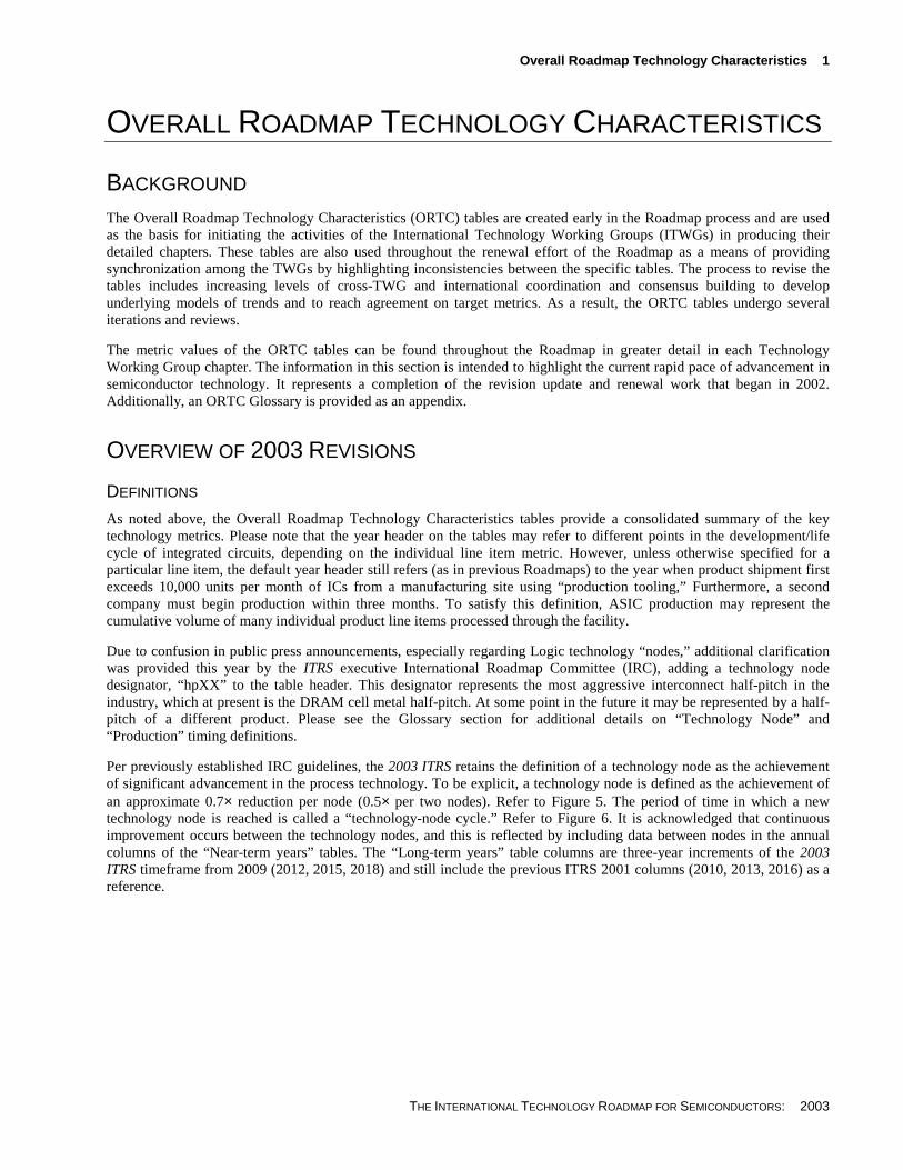
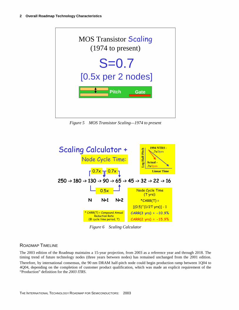
Per previously established IRC guidelines, the 2003 ITRS retains the definition of a technology node as the achievement of significant advancement in the process technology. To be explicit, a technology node is defined as the achievement of an approximate 0.7× reduction per node (0.5× per two nodes). Refer to Figure 5. The period of time in which a new technology node is reached is called a “technology-node cycle.” Refer to Figure 6. It is acknowledged that continuous improvement occurs between the technology nodes, and this is reflected by including data between nodes in the annual columns of the “Near-term years” tables. The “Long-term years” table columns are three-year increments of the 2003 ITRS timeframe from 2009 (2012, 2015, 2018) and still include the previous ITRS 2001 columns (2010, 2013, 2016) as a reference.
2 Overall Roadmap Technology Characteristics
THE INTERNATIONAL TECHNOLOGY ROADMAP FOR SEMICONDUCTORS: 2003
Figure 5 MOS Transistor Scaling—1974 to present
Figure 6 Scaling Calculator
ROADMAP TIMELINE
The 2003 edition of the Roadmap maintains a 15-year projection, from 2003 as a reference year and through 2018. The timing trend of future technology nodes (three years between nodes) has remained unchanged from the 2001 edition.
Therefore, by international consensus, the 90 nm DRAM half-pitch node could begin production ramp between 1Q04 to 4Q04, depending on the completion of customer product qualification, which was made an explicit requirement of the “Production” definition for the 2003 ITRS.
MOS Transistor Scaling(1974 to present)
S=0.7[0.5x per 2 nodes]
Pitch Gate
250 -> 180 -> 130 -> 90 -> 65 -> 45 -> 32 -> 22 -> 16
0.5x
0.7x 0.7x
N N+1 N+2
Node Cycle Time (T yrs):
*CARR(T) =
[(0.5)^(1/2T yrs)] - 1
CARR(3 yrs) = -10.9%
CARR(2 yrs) = -15.9%
* CARR(T) = Compound Annual Reduction Rate
(@ cycle time period, T)
Log
Hal
f-P
itch
Linear Time
1994 NTRS -.7x/3yrs
Actual -.7x/2yrs
Scaling Calculator +Node Cycle Time:
250 -> 180 -> 130 -> 90 -> 65 -> 45 -> 32 -> 22 -> 16
0.5x
0.7x 0.7x
N N+1 N+2
Node Cycle Time (T yrs):
*CARR(T) =
[(0.5)^(1/2T yrs)] - 1
CARR(3 yrs) = -10.9%
CARR(2 yrs) = -15.9%
* CARR(T) = Compound Annual Reduction Rate
(@ cycle time period, T)
Log
Hal
f-P
itch
Linear Time
1994 NTRS -.7x/3yrs
Actual -.7x/2yrs
250 -> 180 -> 130 -> 90 -> 65 -> 45 -> 32 -> 22 -> 16
0.5x
0.7x 0.7x
N N+1 N+2
250 -> 180 -> 130 -> 90 -> 65 -> 45 -> 32 -> 22 -> 16
0.5x
0.7x 0.7x
N N+1 N+2
0.5x
0.7x 0.7x
0.5x
0.7x0.7x 0.7x0.7x
N N+1 N+2N N+1 N+2
Node Cycle Time (T yrs):
*CARR(T) =
[(0.5)^(1/2T yrs)] - 1
CARR(3 yrs) = -10.9%
CARR(2 yrs) = -15.9%
* CARR(T) = Compound Annual Reduction Rate
(@ cycle time period, T)
Log
Hal
f-P
itch
Linear Time
1994 NTRS -.7x/3yrs
Actual -.7x/2yrsL
og H
alf-
Pit
ch
Linear Time
1994 NTRS -.7x/3yrs
Actual -.7x/2yrs
Scaling Calculator +Node Cycle Time:
Overall Roadmap Technology Characteristics 3
THE INTERNATIONAL TECHNOLOGY ROADMAP FOR SEMICONDUCTORS: 2003
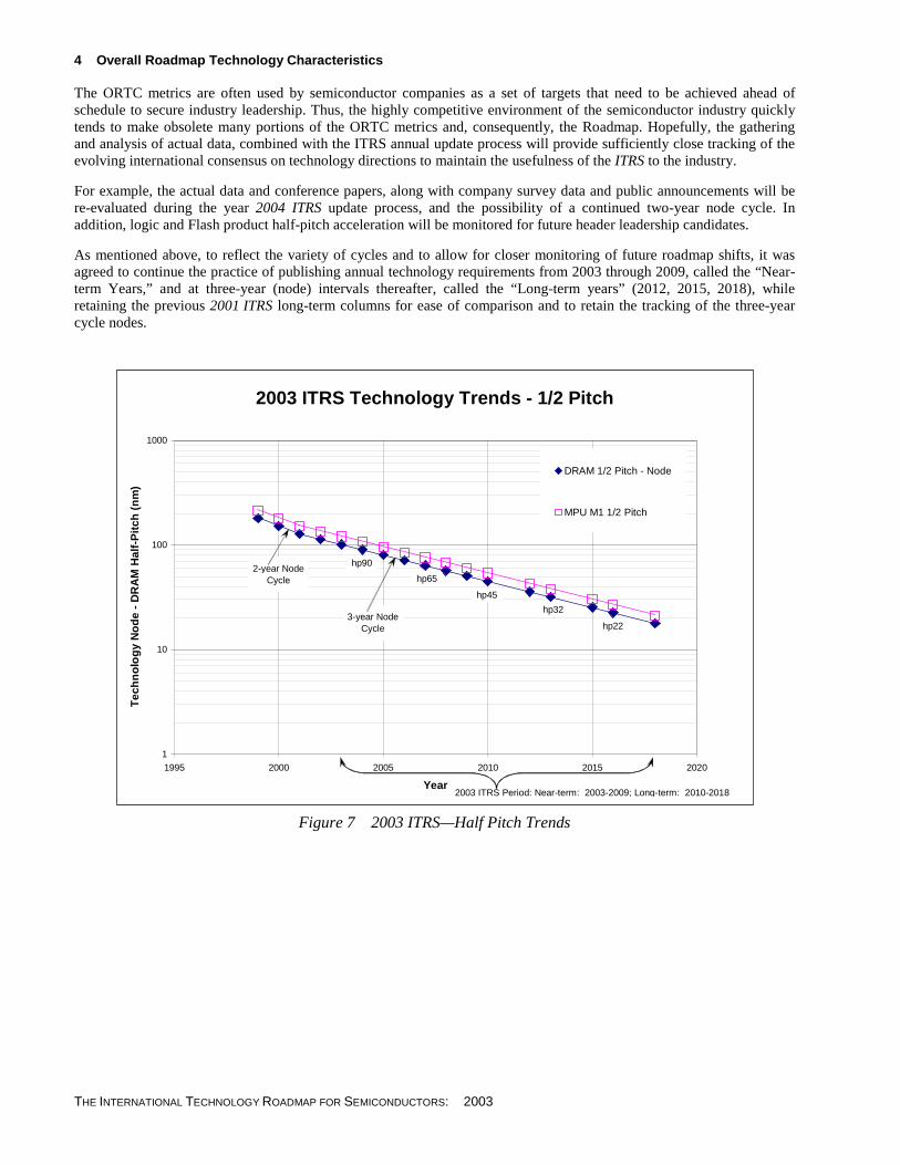
In the 2001 ITRS, the 130 nm node was pulled in an additional year (from 2002 in the 1999 ITRS to 2001), anticipating a continuation of an observed historical two-year technology-node cycle calculated from 350 nm/1995, 250 nm node in 1997, 180 nm node in 1999). Data provided by DRAM manufacturers in 2003, which was based upon the rigorous customer-product-qualified production ramp, indicated that the actual production ramp timing was as follows: 350 nm/1995, 250 nm/1998, 180 nm/2000 and 130 nm/2002. This new data indicates a two-year node cycle timing, but delayed one year from the original 2001 ITRS timing. Data gathered on actual DRAM product ramped in 2003 will confirm if the interim node step is 100 nm, per the 2001 and 2003 ITRS, or 110 nm, which would indicate a two-year cycle step between 130 nm/2002 and 90 nm/2004. Although there is the possibility of a continuation of this new delayed two-year-node cycle trend, the present consensus projects a three-year cycle for DRAM interconnect half-pitch nodes throughout the 2003–2018 Roadmap period, as illustrated in Figure 7.
As mentioned above, the DRAM interconnect half-pitch will continue to be used as the most representative feature of leading-edge semiconductor manufacturing technology for defining the achievement of a technology node. However, future data analysis might indicate an aggressive trend for the lagging MPU, ASIC, and Flash metal and/or polysilicon interconnect half-pitches to pass the DRAM half-pitch after 2004, and become the ITRS header node standard. See Figure 7.
ROUNDED TREND NUMBERS
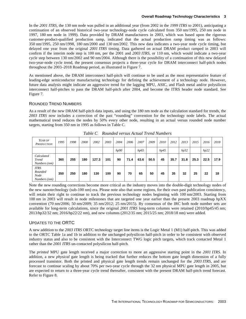
As a result of the new DRAM half-pitch data inputs, and using the 180 nm node as the calculation standard for trends, the 2003 ITRS now includes a correction of the past “rounding” convention for the technology node labels. The actual mathematical trend reduces the nodes by 50% every other node, resulting in an actual versus rounded node number targets, starting from 350 nm in 1995 as follows in Table C.
Table C Rounded versus Actual Trend Numbers
YEAR OF
PRODUCTION 1995 1998 2000 2002 2003 2004 2006 2007 2009 2010 2012 2013 2015 2016 2018
hp90 hp65 hp45 hp32 hp22
Calculated Trend Numbers (nm)
360 255 180 127.3 101 90 71.4 63.6 50.5 45 35.7 31.8 25.3 22.5 17.9
ITRS Rounded Node Numbers (nm)
350 250 180 130 100 90 70 65 50 45 35 32 25 22 18
Note the new rounding corrections become more critical as the industry moves into the double-digit technology nodes of the new nanotechnology (sub-100 nm) era. Please note also that some regions, for their own past publication consistency, will retain their right to continue to track the previous technology nodes beginning with 100 nm/2003. Starting from 100 nm in 2003 will result in node milestones that are targeted one year earlier than the present 2003 roadmap hpXX convention (70 nm/2006; 50 nm/2009; 35 nm/2012; 25 nm/2015). By consensus of the IRC both node number sets are available for long-term calculations, since the original 2001 ITRS long-term columns were retained (2010/hp45/45 nm; 2013/hp32/32 nm; 2016/hp22/22 nm), and new columns (2012/35 nm; 2015/25 nm; 2018/18 nm) were added.
UPDATES TO THE ORTC
A new addition to the 2003 ITRS ORTC technology target line items is the Logic Metal 1 (M1) half-pitch. This was added to the ORTC Table 1a and 1b in addition to the unchanged polysilicon half-pitch in order to be consistent with observed industry status and also to be consistent with the Interconnect TWG logic pitch targets, which track contacted Metal 1 rather than the 2001 ITRS un-contacted polysilicon half-pitch.
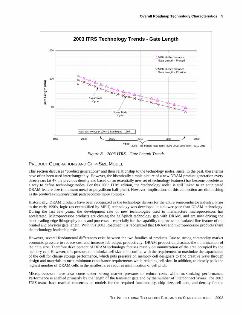
The printed MPU gate length received a major correction to more an aggressive starting point in the 2001 ITRS. In addition, a new physical gate length is being tracked that further reduces the bottom gate length dimension of a fully processed transistor. Both the printed and physical gate length trends remain unchanged for the 2003 ITRS, and are forecast to continue scaling by about 70% per two-year cycle through the 32 nm physical MPU gate length in 2005, but are expected to return to a three-year cycle trend thereafter, consistent with the present DRAM half-pitch trend forecast. Refer to Figure 8.
4 Overall Roadmap Technology Characteristics
THE INTERNATIONAL TECHNOLOGY ROADMAP FOR SEMICONDUCTORS: 2003
The ORTC metrics are often used by semiconductor companies as a set of targets that need to be achieved ahead of schedule to secure industry leadership. Thus, the highly competitive environment of the semiconductor industry quickly tends to make obsolete many portions of the ORTC metrics and, consequently, the Roadmap. Hopefully, the gathering and analysis of actual data, combined with the ITRS annual update process will provide sufficiently close tracking of the evolving international consensus on technology directions to maintain the usefulness of the ITRS to the industry.
For example, the actual data and conference papers, along with company survey data and public announcements will be re-evaluated during the year 2004 ITRS update process, and the possibility of a continued two-year node cycle. In addition, logic and Flash product half-pitch acceleration will be monitored for future header leadership candidates.
As mentioned above, to reflect the variety of cycles and to allow for closer monitoring of future roadmap shifts, it was agreed to continue the practice of publishing annual technology requirements from 2003 through 2009, called the “Near-term Years,” and at three-year (node) intervals thereafter, called the “Long-term years” (2012, 2015, 2018), while retaining the previous 2001 ITRS long-term columns for ease of comparison and to retain the tracking of the three-year cycle nodes.
Figure 7 2003 ITRS—Half Pitch Trends
2003 ITRS Technology Trends - 1/2 Pitch
1
10
100
1000
1995 2000 2005 2010 2015 2020
Year
Tec
hn
olo
gy
No
de
- D
RA
M H
alf-
Pit
ch (
nm
)
DRAM 1/2 Pitch - Node
MPU M1 1/2 Pitch
2003 ITRS Period: Near-term: 2003-2009; Long-term: 2010-2018
hp90
hp65
hp45
hp32
hp22
2-year Node Cycle
3-year Node Cycle
Overall Roadmap Technology Characteristics 5
THE INTERNATIONAL TECHNOLOGY ROADMAP FOR SEMICONDUCTORS: 2003
Figure 8 2003 ITRS—Gate Length Trends
PRODUCT GENERATIONS AND CHIP-SIZE MODEL
This section discusses “product generations” and their relationship to the technology nodes, since, in the past, these terms have often been used interchangeably. However, the historically simple picture of a new DRAM product generation every three years (at 4× the previous density and based on an essentially new set of technology features) has become obsolete as a way to define technology nodes. For this 2003 ITRS edition, the “technology node” is still linked to an anticipated DRAM feature size (minimum metal or polysilicon half-pitch). However, implications of this connection are diminishing as the product evolution/shrink path becomes more complex.
Historically, DRAM products have been recognized as the technology drivers for the entire semiconductor industry. Prior to the early 1990s, logic (as exemplified by MPU) technology was developed at a slower pace than DRAM technology. During the last few years, the development rate of new technologies used to manufacture microprocessors has accelerated. Microprocessor products are closing the half-pitch technology gap with DRAM, and are now driving the most leading-edge lithography tools and processes—especially for the capability to process the isolated-line feature of the printed and physical gate length. With this 2003 Roadmap it is recognized that DRAM and microprocessor products share the technology leadership role.
However, several fundamental differences exist between the two families of products. Due to strong commodity market economic pressure to reduce cost and increase fab output productivity, DRAM product emphasizes the minimization of the chip size. Therefore development of DRAM technology focuses mainly on minimization of the area occupied by the memory cell. However, this pressure to minimize cell size is in conflict with the requirement to maximize the capacitance of the cell for charge storage performance, which puts pressure on memory cell designers to find creative ways through design and materials to meet minimum capacitance requirements while reducing cell size. In addition, to closely pack the highest number of DRAM cells in the smallest area requires minimization of cell pitch.
Microprocessors have also come under strong market pressure to reduce costs while maximizing performance. Performance is enabled primarily by the length of the transistor gate and by the number of interconnect layers. The 2003 ITRS teams have reached consensus on models for the required functionality, chip size, cell area, and density for the
2003 ITRS Technology Trends - Gate Length
1
10
100
1000
1995 2000 2005 2010 2015 2020
Year
Gat
e L
eng
th (
nm
)
MPU Hi-PerformanceGate Length - Printed
MPU Hi-PerformanceGate Length - Physical
Nano-technology (<100nm) Era Begins - 1999
2003 ITRS Period: Near-term: 2003-2009; Long-term: 2010-2018
2-year Node Cycle
3-year Node Cycle
6 Overall Roadmap Technology Characteristics
THE INTERNATIONAL TECHNOLOGY ROADMAP FOR SEMICONDUCTORS: 2003
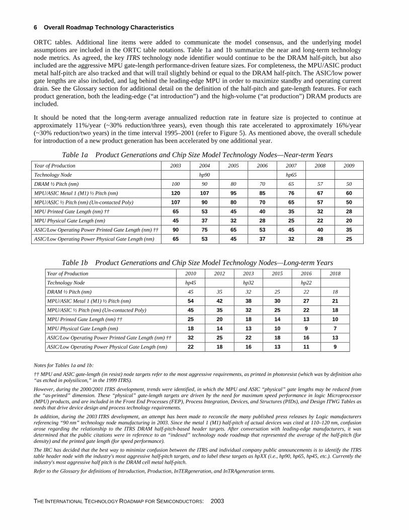
ORTC tables. Additional line items were added to communicate the model consensus, and the underlying model assumptions are included in the ORTC table notations. Table 1a and 1b summarize the near and long-term technology node metrics. As agreed, the key ITRS technology node identifier would continue to be the DRAM half-pitch, but also included are the aggressive MPU gate-length performance-driven feature sizes. For completeness, the MPU/ASIC product metal half-pitch are also tracked and that will trail slightly behind or equal to the DRAM half-pitch. The ASIC/low power gate lengths are also included, and lag behind the leading-edge MPU in order to maximize standby and operating current drain. See the Glossary section for additional detail on the definition of the half-pitch and gate-length features. For each product generation, both the leading-edge (“at introduction”) and the high-volume (“at production”) DRAM products are included.
It should be noted that the long-term average annualized reduction rate in feature size is projected to continue at approximately 11%/year (~30% reduction/three years), even though this rate accelerated to approximately 16%/year (~30% reduction/two years) in the time interval 1995–2001 (refer to Figure 5). As mentioned above, the overall schedule for introduction of a new product generation has been accelerated by one additional year.
Table 1a Product Generations and Chip Size Model Technology Nodes—Near-term Years
Year of Production 2003 2004 2005 2006 2007 2008 2009
Technology Node hp90 hp65
DRAM ½ Pitch (nm) 100 90 80 70 65 57 50
MPU/ASIC Metal 1 (M1) ½ Pitch (nm) 120 107 95 85 76 67 60
MPU/ASIC ½ Pitch (nm) (Un-contacted Poly) 107 90 80 70 65 57 50
MPU Printed Gate Length (nm) †† 65 53 45 40 35 32 28
MPU Physical Gate Length (nm) 45 37 32 28 25 22 20
ASIC/Low Operating Power Printed Gate Length (nm) †† 90 75 65 53 45 40 35
ASIC/Low Operating Power Physical Gate Length (nm) 65 53 45 37 32 28 25
Table 1b Product Generations and Chip Size Model Technology Nodes—Long-term Years
Year of Production 2010 2012 2013 2015 2016 2018
Technology Node hp45 hp32 hp22
DRAM ½ Pitch (nm) 45 35 32 25 22 18
MPU/ASIC Metal 1 (M1) ½ Pitch (nm) 54 42 38 30 27 21
MPU/ASIC ½ Pitch (nm) (Un-contacted Poly) 45 35 32 25 22 18
MPU Printed Gate Length (nm) †† 25 20 18 14 13 10
MPU Physical Gate Length (nm) 18 14 13 10 9 7
ASIC/Low Operating Power Printed Gate Length (nm) †† 32 25 22 18 16 13
ASIC/Low Operating Power Physical Gate Length (nm) 22 18 16 13 11 9
Notes for Tables 1a and 1b:
†† MPU and ASIC gate-length (in resist) node targets refer to the most aggressive requirements, as printed in photoresist (which was by definition also “as etched in polysilicon,” in the 1999 ITRS).
However, during the 2000/2001 ITRS development, trends were identified, in which the MPU and ASIC “physical” gate lengths may be reduced from the “as-printed” dimension. These “physical” gate-length targets are driven by the need for maximum speed performance in logic Microprocessor (MPU) products, and are included in the Front End Processes (FEP), Process Integration, Devices, and Structures (PIDs), and Design ITWG Tables as needs that drive device design and process technology requirements.
In addition, during the 2003 ITRS development, an attempt has been made to reconcile the many published press releases by Logic manufacturers referencing “90 nm” technology node manufacturing in 2003. Since the metal 1 (M1) half-pitch of actual devices was cited at 110–120 nm, confusion arose regarding the relationship to the ITRS DRAM half-pitch-based header targets. After conversation with leading-edge manufacturers, it was determined that the public citations were in reference to an “indexed” technology node roadmap that represented the average of the half-pitch (for density) and the printed gate length (for speed performance).
The IRC has decided that the best way to minimize confusion between the ITRS and individual company public announcements is to identify the ITRS table header node with the industry's most aggressive half-pitch targets, and to label these targets as hpXX (i.e., hp90, hp65, hp45, etc.). Currently the industry's most aggressive half pitch is the DRAM cell metal half-pitch.
Refer to the Glossary for definitions of Introduction, Production, InTERgeneration, and InTRAgeneration terms.
Overall Roadmap Technology Characteristics 7
THE INTERNATIONAL TECHNOLOGY ROADMAP FOR SEMICONDUCTORS: 2003
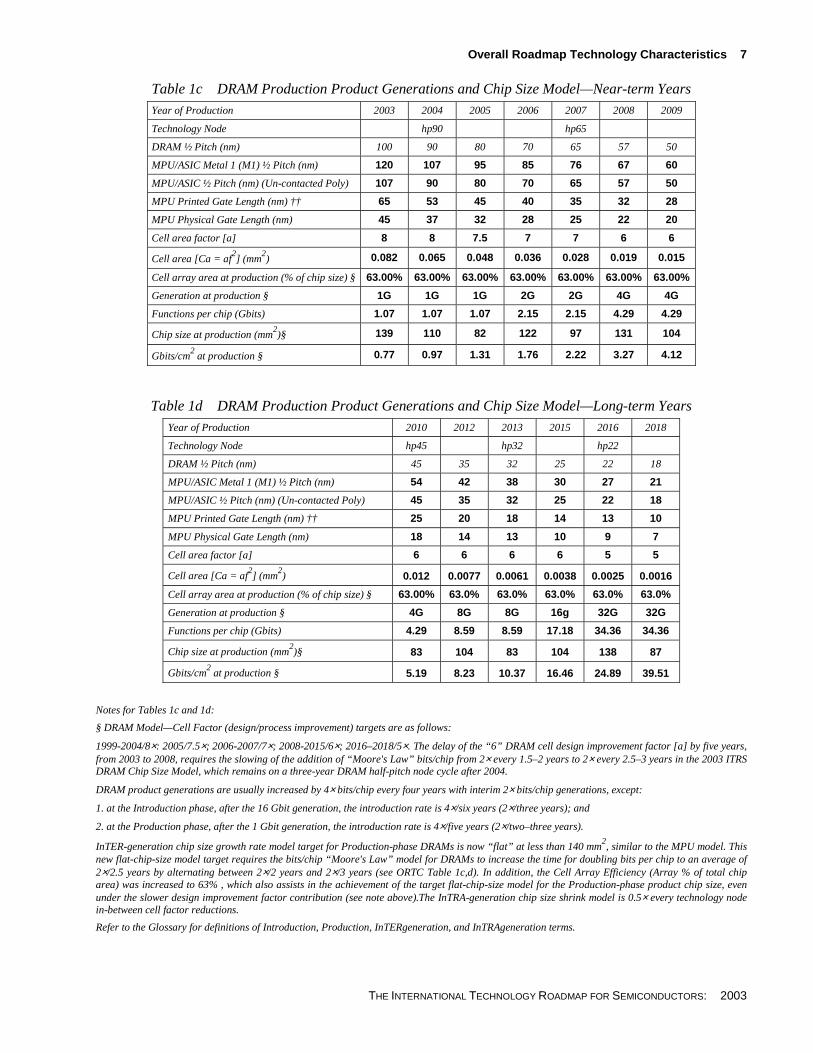
Table 1c DRAM Production Product Generations and Chip Size Model—Near-term Years
Year of Production 2003 2004 2005 2006 2007 2008 2009
Technology Node hp90 hp65
DRAM ½ Pitch (nm) 100 90 80 70 65 57 50
MPU/ASIC Metal 1 (M1) ½ Pitch (nm) 120 107 95 85 76 67 60
MPU/ASIC ½ Pitch (nm) (Un-contacted Poly) 107 90 80 70 65 57 50
MPU Printed Gate Length (nm) †† 65 53 45 40 35 32 28
MPU Physical Gate Length (nm) 45 37 32 28 25 22 20
Cell area factor [a] 8 8 7.5 7 7 6 6
Cell area [Ca = af2] (mm
2) 0.082 0.065 0.048 0.036 0.028 0.019 0.015
Cell array area at production (% of chip size) § 63.00% 63.00% 63.00% 63.00% 63.00% 63.00% 63.00%
Generation at production § 1G 1G 1G 2G 2G 4G 4G
Functions per chip (Gbits) 1.07 1.07 1.07 2.15 2.15 4.29 4.29
Chip size at production (mm2)§ 139 110 82 122 97 131 104
Gbits/cm2 at production § 0.77 0.97 1.31 1.76 2.22 3.27 4.12
Table 1d DRAM Production Product Generations and Chip Size Model—Long-term Years
Year of Production 2010 2012 2013 2015 2016 2018
Technology Node hp45 hp32 hp22
DRAM ½ Pitch (nm) 45 35 32 25 22 18
MPU/ASIC Metal 1 (M1) ½ Pitch (nm) 54 42 38 30 27 21
MPU/ASIC ½ Pitch (nm) (Un-contacted Poly) 45 35 32 25 22 18
MPU Printed Gate Length (nm) †† 25 20 18 14 13 10
MPU Physical Gate Length (nm) 18 14 13 10 9 7
Cell area factor [a] 6 6 6 6 5 5
Cell area [Ca = af2] (mm
2) 0.012 0.0077 0.0061 0.0038 0.0025 0.0016
Cell array area at production (% of chip size) § 63.00% 63.0% 63.0% 63.0% 63.0% 63.0%
Generation at production § 4G 8G 8G 16g 32G 32G
Functions per chip (Gbits) 4.29 8.59 8.59 17.18 34.36 34.36
Chip size at production (mm2)§ 83 104 83 104 138 87
Gbits/cm2 at production § 5.19 8.23 10.37 16.46 24.89 39.51
Notes for Tables 1c and 1d:
§ DRAM Model—Cell Factor (design/process improvement) targets are as follows:
1999-2004/8×: 2005/7.5×; 2006-2007/7×; 2008-2015/6×; 2016–2018/5×. The delay of the “6” DRAM cell design improvement factor [a] by five years, from 2003 to 2008, requires the slowing of the addition of “Moore's Law” bits/chip from 2× every 1.5–2 years to 2× every 2.5–3 years in the 2003 ITRS DRAM Chip Size Model, which remains on a three-year DRAM half-pitch node cycle after 2004.
DRAM product generations are usually increased by 4× bits/chip every four years with interim 2× bits/chip generations, except:
1. at the Introduction phase, after the 16 Gbit generation, the introduction rate is 4×/six years (2×/three years); and
2. at the Production phase, after the 1 Gbit generation, the introduction rate is 4×/five years (2×/two–three years).
InTER-generation chip size growth rate model target for Production-phase DRAMs is now “flat” at less than 140 mm2, similar to the MPU model. This
new flat-chip-size model target requires the bits/chip “Moore's Law” model for DRAMs to increase the time for doubling bits per chip to an average of 2×/2.5 years by alternating between 2×/2 years and 2×/3 years (see ORTC Table 1c,d). In addition, the Cell Array Efficiency (Array % of total chip area) was increased to 63% , which also assists in the achievement of the target flat-chip-size model for the Production-phase product chip size, even under the slower design improvement factor contribution (see note above).The InTRA-generation chip size shrink model is 0.5× every technology node in-between cell factor reductions.
Refer to the Glossary for definitions of Introduction, Production, InTERgeneration, and InTRAgeneration terms.
8 Overall Roadmap Technology Characteristics
THE INTERNATIONAL TECHNOLOGY ROADMAP FOR SEMICONDUCTORS: 2003
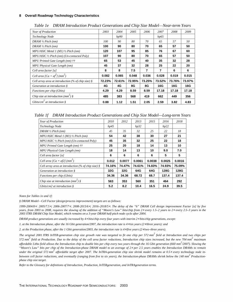
Table 1e DRAM Introduction Product Generations and Chip Size Model—Near-term Years
Year of Production 2003 2004 2005 2006 2007 2008 2009
Technology Node hp90 hp65
DRAM ½ Pitch (nm) 100 90 80 70 65 57 50
DRAM ½ Pitch (nm) 100 90 80 70 65 57 50
MPU/ASIC Metal 1 (M1) ½ Pitch (nm) 120 107 95 85 76 67 60
MPU/ASIC ½ Pitch (nm) (Un-contacted Poly) 107 90 80 70 65 57 50
MPU Printed Gate Length (nm) †† 65 53 45 40 35 32 28
MPU Physical Gate Length (nm) 45 37 32 28 25 22 20
Cell area factor [a] 8 8 7.5 7 7 6 6
Cell area [Ca = af2] (mm
2) 0.082 0.065 0.048 0.036 0.028 0.019 0.015
Cell array area at introduction (% of chip size) § 72.23% 72.61% 72.95% 73.25% 73.52% 73.76% 73.97%
Generation at introduction § 4G 4G 8G 8G 16G 16G 16G
Functions per chip (Gbits) 4.29 4.29 8.59 8.59 17.18 17.18 17.18
Chip size at introduction (mm2) § 485 383 568 419 662 449 356
Gbits/cm2 at introduction § 0.88 1.12 1.51 2.05 2.59 3.82 4.83
Table 1f DRAM Introduction Product Generations and Chip Size Model—Long-term Years
Year of Production 2010 2012 2013 2015 2016 2018
Technology Node hp45 hp32 hp22
DRAM ½ Pitch (nm) 45 35 32 25 22 18
MPU/ASIC Metal 1 (M1) ½ Pitch (nm) 54 42 38 30 27 21
MPU/ASIC ½ Pitch (nm) (Un-contacted Poly) 45 35 32 25 22 18
MPU Printed Gate Length (nm) †† 25 20 18 14 13 10
MPU Physical Gate Length (nm) 18 14 13 10 9.0 7.0
Cell area factor [a] 6 6 6 6 5 5
Cell area [Ca = af2] (mm2) 0.012 0.0077 0.0061 0.0038 0.0025 0.0016
Cell array area at introduction (% of chip size) § 74.16% 74.47% 74.61% 74.83% 74.93% 75.09%
Generation at introduction § 32G 32G 64G 64G 128G 128G
Functions per chip (Gbits) 34.36 34.36 68.72 68.7 137.4 137.4
Chip size at introduction (mm2) § 563 353 560 351 464 292
Gbits/cm2 at introduction § 5.2 8.2 10.4 16.5 24.9 39.5
Notes for Tables 1e and 1f:
§ DRAM Model—Cell Factor (design/process improvement) targets are as follows:
1999-2004/8×: 2005/7.5×; 2006-2007/7×; 2008-2015/6×; 2016–2018/5×. The delay of the “6” DRAM Cell design improvement Factor [a] by five years, from 2003 to 2008, requires the slowing of the addition of “Moore's Law” bits/chip from 2× every 1.5–2 years to 2× every 2.5–3 years in the 2003 ITRS DRAM Chip Size Model, which remains on a 3-year DRAM half-pitch node cycle after 2004.
DRAM product generations are usually increased by 4× bits/chip every four years with interim 2× bits/chip generations, except:
1. at the Introduction phase, after the 16 Gbit generation/2007, the introduction rate is 4×/six years (2×/three years); and
2. at the Production phase, after the 1 Gbit generation/2003, the introduction rate is 4×/five years (2×/two–three years).
The original 2001 ITRS InTER-generation chip size growth rate was targeted to fit one chip per 572 mm2 field at Introduction and two chips per
572 mm2 field at Production. Due to the delay of the cell area factor reductions, Introduction chip sizes increased, but the new 704 mm
2 maximum
affordable Litho field allows the Introduction chip to double bits per chip every two years through the 16 Gbit generation (660 mm2/2007). Slowing the
“Moore's Law” bits per chip of the Introduction-phase DRAM model to an average of 2× per 2.5 years enables the Introduction DRAMs to remain under the original 572 mm
2 affordable target after 2007. The InTRA-generation chip size shrink model remains at 0.5× every technology node in-
between cell factor reductions, and eventually (ranging from five to six years), the Introduction-phase DRAMs shrink below the 140 mm2 Production-
phase chip size target.
Refer to the Glossary for definitions of Introduction, Production, InTERgeneration, and InTRAgeneration terms.
Overall Roadmap Technology Characteristics 9
THE INTERNATIONAL TECHNOLOGY ROADMAP FOR SEMICONDUCTORS: 2003
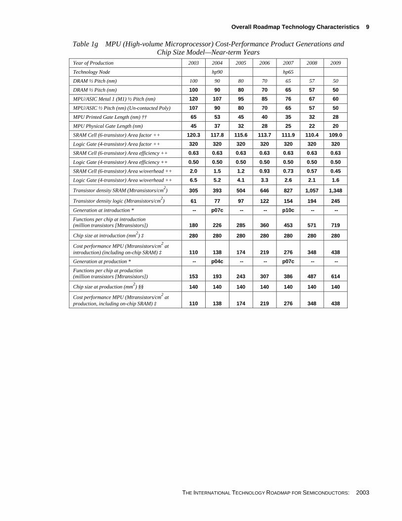
Table 1g MPU (High-volume Microprocessor) Cost-Performance Product Generations and Chip Size Model—Near-term Years
Year of Production 2003 2004 2005 2006 2007 2008 2009
Technology Node hp90 hp65
DRAM ½ Pitch (nm) 100 90 80 70 65 57 50
DRAM ½ Pitch (nm) 100 90 80 70 65 57 50
MPU/ASIC Metal 1 (M1) ½ Pitch (nm) 120 107 95 85 76 67 60
MPU/ASIC ½ Pitch (nm) (Un-contacted Poly) 107 90 80 70 65 57 50
MPU Printed Gate Length (nm) †† 65 53 45 40 35 32 28
MPU Physical Gate Length (nm) 45 37 32 28 25 22 20
SRAM Cell (6-transistor) Area factor ++ 120.3 117.8 115.6 113.7 111.9 110.4 109.0
Logic Gate (4-transistor) Area factor ++ 320 320 320 320 320 320 320
SRAM Cell (6-transistor) Area efficiency ++ 0.63 0.63 0.63 0.63 0.63 0.63 0.63
Logic Gate (4-transistor) Area efficiency ++ 0.50 0.50 0.50 0.50 0.50 0.50 0.50
SRAM Cell (6-transistor) Area w/overhead ++ 2.0 1.5 1.2 0.93 0.73 0.57 0.45
Logic Gate (4-transistor) Area w/overhead ++ 6.5 5.2 4.1 3.3 2.6 2.1 1.6
Transistor density SRAM (Mtransistors/cm2) 305 393 504 646 827 1,057 1,348
Transistor density logic (Mtransistors/cm2) 61 77 97 122 154 194 245
Generation at introduction * -- p07c -- -- p10c -- --
Functions per chip at introduction (million transistors [Mtransistors]) 180 226 285 360 453 571 719
Chip size at introduction (mm2) ‡ 280 280 280 280 280 280 280
Cost performance MPU (Mtransistors/cm2 at
introduction) (including on-chip SRAM) ‡ 110 138 174 219 276 348 438
Generation at production * -- p04c -- -- p07c -- --
Functions per chip at production (million transistors [Mtransistors]) 153 193 243 307 386 487 614
Chip size at production (mm2) §§ 140 140 140 140 140 140 140
Cost performance MPU (Mtransistors/cm2 at
production, including on-chip SRAM) ‡ 110 138 174 219 276 348 438
10 Overall Roadmap Technology Characteristics
THE INTERNATIONAL TECHNOLOGY ROADMAP FOR SEMICONDUCTORS: 2003
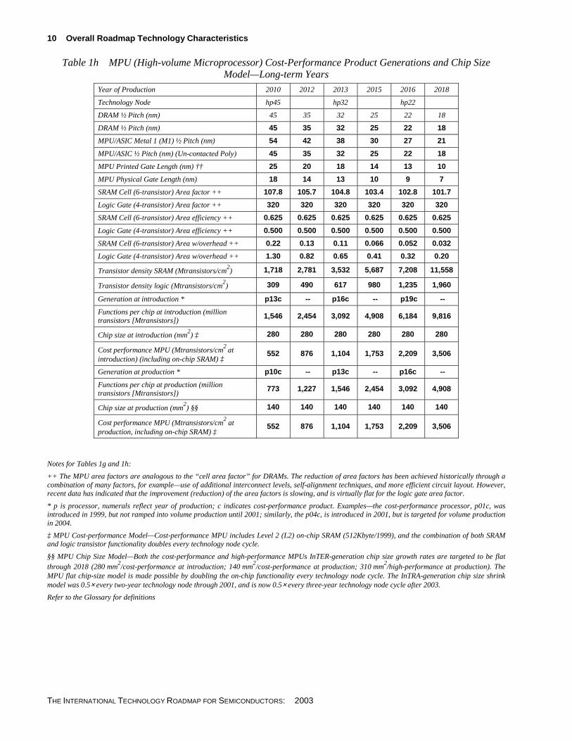
Table 1h MPU (High-volume Microprocessor) Cost-Performance Product Generations and Chip Size Model—Long-term Years
Year of Production 2010 2012 2013 2015 2016 2018
Technology Node hp45 hp32 hp22
DRAM ½ Pitch (nm) 45 35 32 25 22 18
DRAM ½ Pitch (nm) 45 35 32 25 22 18
MPU/ASIC Metal 1 (M1) ½ Pitch (nm) 54 42 38 30 27 21
MPU/ASIC ½ Pitch (nm) (Un-contacted Poly) 45 35 32 25 22 18
MPU Printed Gate Length (nm) †† 25 20 18 14 13 10
MPU Physical Gate Length (nm) 18 14 13 10 9 7
SRAM Cell (6-transistor) Area factor ++ 107.8 105.7 104.8 103.4 102.8 101.7
Logic Gate (4-transistor) Area factor ++ 320 320 320 320 320 320
SRAM Cell (6-transistor) Area efficiency ++ 0.625 0.625 0.625 0.625 0.625 0.625
Logic Gate (4-transistor) Area efficiency ++ 0.500 0.500 0.500 0.500 0.500 0.500
SRAM Cell (6-transistor) Area w/overhead ++ 0.22 0.13 0.11 0.066 0.052 0.032
Logic Gate (4-transistor) Area w/overhead ++ 1.30 0.82 0.65 0.41 0.32 0.20
Transistor density SRAM (Mtransistors/cm2) 1,718 2,781 3,532 5,687 7,208 11,558
Transistor density logic (Mtransistors/cm2) 309 490 617 980 1,235 1,960
Generation at introduction * p13c -- p16c -- p19c --
Functions per chip at introduction (million transistors [Mtransistors])
1,546 2,454 3,092 4,908 6,184 9,816
Chip size at introduction (mm2) ‡ 280 280 280 280 280 280
Cost performance MPU (Mtransistors/cm2
at introduction) (including on-chip SRAM) ‡
552 876 1,104 1,753 2,209 3,506
Generation at production * p10c -- p13c -- p16c --
Functions per chip at production (million transistors [Mtransistors])
773 1,227 1,546 2,454 3,092 4,908
Chip size at production (mm2) §§ 140 140 140 140 140 140
Cost performance MPU (Mtransistors/cm2 at
production, including on-chip SRAM) ‡ 552 876 1,104 1,753 2,209 3,506
Notes for Tables 1g and 1h:
++ The MPU area factors are analogous to the “cell area factor” for DRAMs. The reduction of area factors has been achieved historically through a combination of many factors, for example—use of additional interconnect levels, self-alignment techniques, and more efficient circuit layout. However, recent data has indicated that the improvement (reduction) of the area factors is slowing, and is virtually flat for the logic gate area factor.
* p is processor, numerals reflect year of production; c indicates cost-performance product. Examples—the cost-performance processor, p01c, was introduced in 1999, but not ramped into volume production until 2001; similarly, the p04c, is introduced in 2001, but is targeted for volume production in 2004.
‡ MPU Cost-performance Model—Cost-performance MPU includes Level 2 (L2) on-chip SRAM (512Kbyte/1999), and the combination of both SRAM and logic transistor functionality doubles every technology node cycle.
§§ MPU Chip Size Model—Both the cost-performance and high-performance MPUs InTER-generation chip size growth rates are targeted to be flat through 2018 (280 mm
2/cost-performance at introduction; 140 mm
2/cost-performance at production; 310 mm
2/high-performance at production). The
MPU flat chip-size model is made possible by doubling the on-chip functionality every technology node cycle. The InTRA-generation chip size shrink model was 0.5× every two-year technology node through 2001, and is now 0.5× every three-year technology node cycle after 2003.
Refer to the Glossary for definitions
Overall Roadmap Technology Characteristics 11
THE INTERNATIONAL TECHNOLOGY ROADMAP FOR SEMICONDUCTORS: 2003
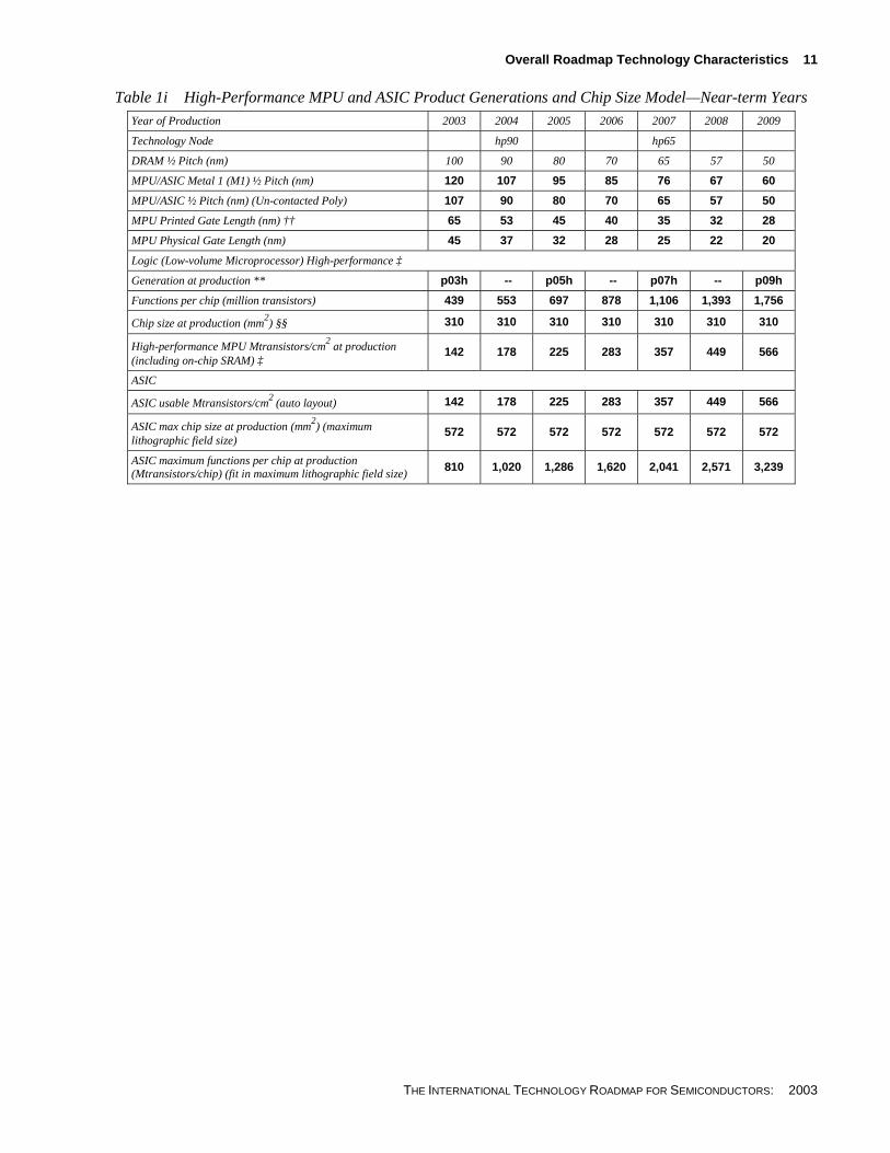
Table 1i High-Performance MPU and ASIC Product Generations and Chip Size Model—Near-term Years
Year of Production 2003 2004 2005 2006 2007 2008 2009
Technology Node hp90 hp65
DRAM ½ Pitch (nm) 100 90 80 70 65 57 50
MPU/ASIC Metal 1 (M1) ½ Pitch (nm) 120 107 95 85 76 67 60
MPU/ASIC ½ Pitch (nm) (Un-contacted Poly) 107 90 80 70 65 57 50
MPU Printed Gate Length (nm) †† 65 53 45 40 35 32 28
MPU Physical Gate Length (nm) 45 37 32 28 25 22 20
Logic (Low-volume Microprocessor) High-performance ‡
Generation at production ** p03h -- p05h -- p07h -- p09h
Functions per chip (million transistors) 439 553 697 878 1,106 1,393 1,756
Chip size at production (mm2) §§ 310 310 310 310 310 310 310
High-performance MPU Mtransistors/cm2 at production
(including on-chip SRAM) ‡ 142 178 225 283 357 449 566
ASIC
ASIC usable Mtransistors/cm2
(auto layout) 142 178 225 283 357 449 566
ASIC max chip size at production (mm2) (maximum
lithographic field size) 572 572 572 572 572 572 572
ASIC maximum functions per chip at production (Mtransistors/chip) (fit in maximum lithographic field size)
810 1,020 1,286 1,620 2,041 2,571 3,239
12 Overall Roadmap Technology Characteristics
THE INTERNATIONAL TECHNOLOGY ROADMAP FOR SEMICONDUCTORS: 2003
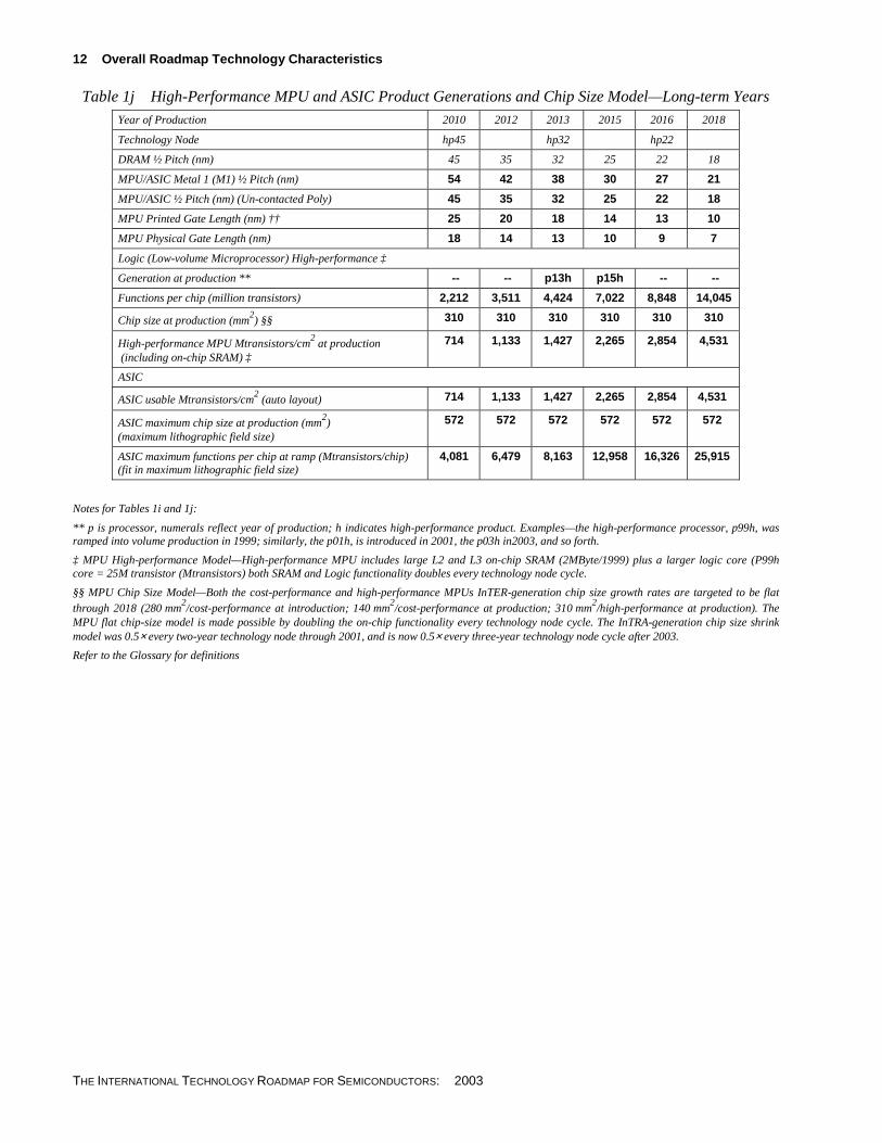
Table 1j High-Performance MPU and ASIC Product Generations and Chip Size Model—Long-term Years
Year of Production 2010 2012 2013 2015 2016 2018
Technology Node hp45 hp32 hp22
DRAM ½ Pitch (nm) 45 35 32 25 22 18
MPU/ASIC Metal 1 (M1) ½ Pitch (nm) 54 42 38 30 27 21
MPU/ASIC ½ Pitch (nm) (Un-contacted Poly) 45 35 32 25 22 18
MPU Printed Gate Length (nm) †† 25 20 18 14 13 10
MPU Physical Gate Length (nm) 18 14 13 10 9 7
Logic (Low-volume Microprocessor) High-performance ‡
Generation at production ** -- -- p13h p15h -- --
Functions per chip (million transistors) 2,212 3,511 4,424 7,022 8,848 14,045
Chip size at production (mm2) §§ 310 310 310 310 310 310
High-performance MPU Mtransistors/cm2 at production
(including on-chip SRAM) ‡
714 1,133 1,427 2,265 2,854 4,531
ASIC
ASIC usable Mtransistors/cm2 (auto layout) 714 1,133 1,427 2,265 2,854 4,531
ASIC maximum chip size at production (mm2)
(maximum lithographic field size)
572 572 572 572 572 572
ASIC maximum functions per chip at ramp (Mtransistors/chip) (fit in maximum lithographic field size)
4,081 6,479 8,163 12,958 16,326 25,915
Notes for Tables 1i and 1j:
** p is processor, numerals reflect year of production; h indicates high-performance product. Examples—the high-performance processor, p99h, was ramped into volume production in 1999; similarly, the p01h, is introduced in 2001, the p03h in2003, and so forth.
‡ MPU High-performance Model—High-performance MPU includes large L2 and L3 on-chip SRAM (2MByte/1999) plus a larger logic core (P99h core = 25M transistor (Mtransistors) both SRAM and Logic functionality doubles every technology node cycle.
§§ MPU Chip Size Model—Both the cost-performance and high-performance MPUs InTER-generation chip size growth rates are targeted to be flat through 2018 (280 mm
2/cost-performance at introduction; 140 mm
2/cost-performance at production; 310 mm
2/high-performance at production). The
MPU flat chip-size model is made possible by doubling the on-chip functionality every technology node cycle. The InTRA-generation chip size shrink model was 0.5× every two-year technology node through 2001, and is now 0.5× every three-year technology node cycle after 2003.
Refer to the Glossary for definitions

Overall Roadmap Technology Characteristics 13
THE INTERNATIONAL TECHNOLOGY ROADMAP FOR SEMICONDUCTORS: 2003
CHIP-SIZE, LITHOGRAPHIC-FIELD, AND WAFER-SIZE TRENDS
Despite the continuous reduction in feature size of about 30% every three years, the size of first DRAM product demonstration in technical forums such as the IEEE International Solid State Circuits Conference (ISSCC) has continued to double every six years (an increase of about 12%/year). This increase in chip area has been necessary to accommodate 59% more bits/capacitors/transistors per year in accordance with Moore's Law (historically doubling functions per chip every 1.5–2 years). However, to maintain the historical trend of reducing cost/function by ~25–30%/year, it is necessary to continuously enhance equipment productivity, increase manufacturing yields, use the largest wafer size available, and, most of all, increase the number of chips available on a wafer.
The increase in the gross number of chips available on a wafer is primarily obtained by reducing the area of the chip by means of a combination of smaller feature size (shrink/scaling) and product/process redesign (compaction). For instance, using the latest models, it is forecast that the introduction chip area of a cost-effective product generation [which doubles the inter-generation (generation-to-generation) functionality every two years] must either remain as flat as possible. Furthermore, the area must be shrunk at an intra-generation (within a generation) annual reduction rate of 50% (the square of the .7× lithography reduction rate) during every technology node period.
In order for affordable DRAM products to achieve virtually flat intra-generation chip-sizes, they must also maintain a cell area array efficiency ratio of 63% of total chip area. Therefore, DRAM products require reduction of cell area design factors (cell area in units of minimum-feature-size-squared). The PIDS and FEP ITWGs have provided member survey data for the array efficiency targets, the cell area factors, and bits per chip. In addition, detailed challenges and needs for solutions to meet the aggressive cell area goals are documented in the Front End Processes chapter. Due to the importance of tracking/coordinating these new challenges, the DRAM cell area factor, the target cell sizes, and the cell array area percentage of total chip-size line items will continue to be tracked in ORTC Tables 1c, d, e, and f. (also refer to the Glossary for additional details). Notably, the reduction rate of DRAM cell area factors for the 2003 ITRS models has been slowed significantly (the 6 factor moved from 2003 to 2008, and the 4 factor has been increased to 5 and moved from 2011 to 2016). In order to maintain the goal of flat chip sizes, the 2003 ITRS DRAM chip size model now includes more aggressive array efficiency targets, and the rate of increase of “Moore’s Law” bits per chip targets has been slowed from 2× every three years to 2× every three years.
In the 2001 ITRS the Design ITWG improved the MPU chip size model to update with the latest transistor densities, large on-chip SRAM, and smaller target chip sizes. The Design ITWG has also added additional detail to the model, including transistor design improvement factors. The Design ITWG notes that design improvements occur at a slow rate in SRAM transistors and very little in logic gate transistors. Almost all the “shrink” and density improvement comes from lithography-enabled interconnect half-pitch scaling alone.
The present 2003 ITRS MPU chip size model is unchanged from the 2001 ITRS, and continues to reflect the additional competitive requirements for affordability and power management by targeting flat chip size trends for both high-performance MPUs (310 mm2) and cost-performance MPUs (140 mm2). Due to the MPU two-year-cycle half-pitch “catch-up phase” through the year 2004, the MPU products may be able to maintain flat chip sizes due to lithography improvements alone. However, after 2004, the inter-generation MPU chip size model, which is indexed to the ITRS technology node, can remain flat only by slowing the rate of on-chip transistors to double every technology node.
Due to the forecasted return to a three-year technology node cycle, the present MPU chip-size model slows the Moore's Law rate of on-chip transistors to 2× every three years. In order to maintain a flat chip size target and also return to the historical doubling every two years of on-chip functionality (transistors), MPU chip and process designers must add additional design/process improvements to the fundamental lithography-based scaling trends. The new target metrics of the MPU model are summarized in Tables 1g, h, i, and j.
To improve productivity, it is necessary to increase the output of good chips at each step in the fabrication process. The ability of printing multiple chips in a single exposure is a key productivity driver and is determined by the field size of the lithographic tool and the size and aspect ratio of the chips being printed on the wafer. In the past, lithography exposure field sizes doubled every other technology node to meet the demand for increasing chip sizes. The result was the achievement of very large step-and-scan fields (25×32 = 800 mm2) by 1999. However, the Lithography ITWG indicates that maintaining the large field size under continued reduction of exposure features is increasing costs dramatically. Therefore, the ITWG forecasts of a requirement for the economically affordable lithography field was reduced to 572 mm2 (22×26) by the 90 nm node. After addition review, the Lithography TWG increased the “Affordable” field size to 704 mm2 (22×32) for the 2003 ITRS. That trend is shown in Tables 2a and b.
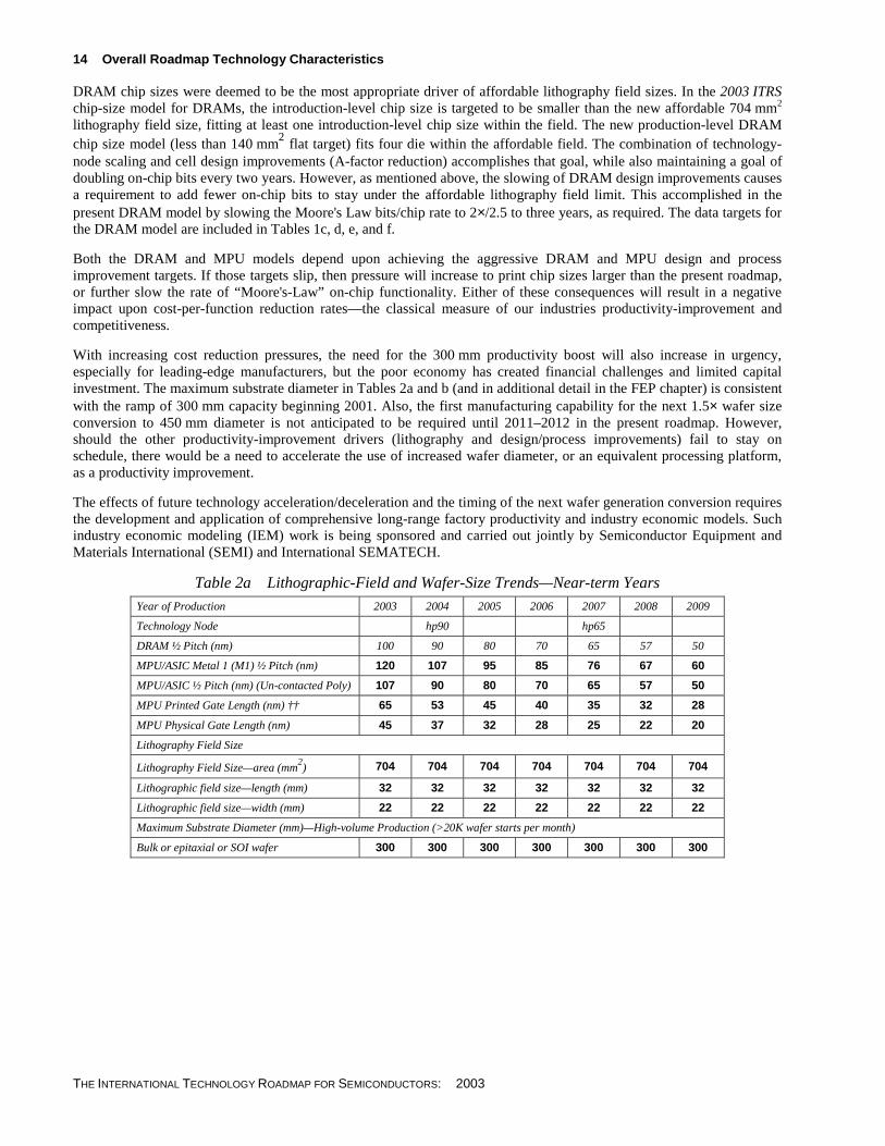
14 Overall Roadmap Technology Characteristics
THE INTERNATIONAL TECHNOLOGY ROADMAP FOR SEMICONDUCTORS: 2003
DRAM chip sizes were deemed to be the most appropriate driver of affordable lithography field sizes. In the 2003 ITRS chip-size model for DRAMs, the introduction-level chip size is targeted to be smaller than the new affordable 704 mm2 lithography field size, fitting at least one introduction-level chip size within the field. The new production-level DRAM chip size model (less than 140 mm2 flat target) fits four die within the affordable field. The combination of technology-node scaling and cell design improvements (A-factor reduction) accomplishes that goal, while also maintaining a goal of doubling on-chip bits every two years. However, as mentioned above, the slowing of DRAM design improvements causes a requirement to add fewer on-chip bits to stay under the affordable lithography field limit. This accomplished in the present DRAM model by slowing the Moore's Law bits/chip rate to 2×/2.5 to three years, as required. The data targets for the DRAM model are included in Tables 1c, d, e, and f.
Both the DRAM and MPU models depend upon achieving the aggressive DRAM and MPU design and process improvement targets. If those targets slip, then pressure will increase to print chip sizes larger than the present roadmap, or further slow the rate of “Moore's-Law” on-chip functionality. Either of these consequences will result in a negative impact upon cost-per-function reduction rates—the classical measure of our industries productivity-improvement and competitiveness.
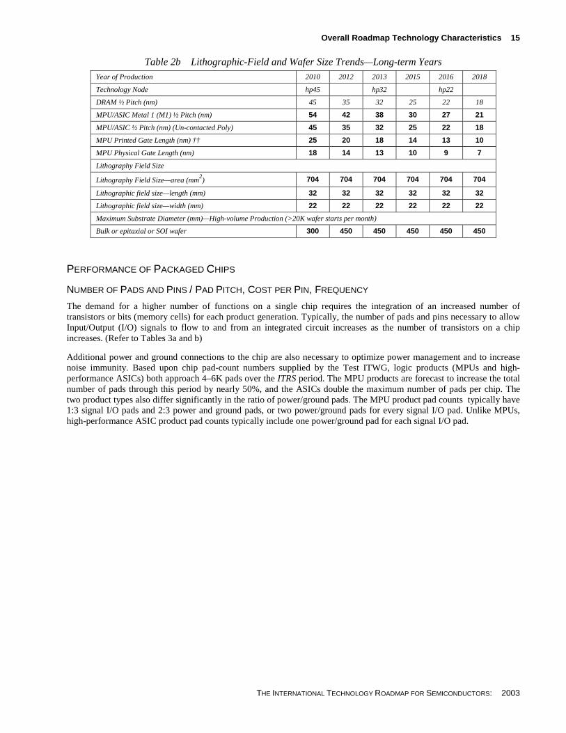
With increasing cost reduction pressures, the need for the 300 mm productivity boost will also increase in urgency, especially for leading-edge manufacturers, but the poor economy has created financial challenges and limited capital investment. The maximum substrate diameter in Tables 2a and b (and in additional detail in the FEP chapter) is consistent with the ramp of 300 mm capacity beginning 2001. Also, the first manufacturing capability for the next 1.5× wafer size conversion to 450 mm diameter is not anticipated to be required until 2011–2012 in the present roadmap. However, should the other productivity-improvement drivers (lithography and design/process improvements) fail to stay on schedule, there would be a need to accelerate the use of increased wafer diameter, or an equivalent processing platform, as a productivity improvement.
The effects of future technology acceleration/deceleration and the timing of the next wafer generation conversion requires the development and application of comprehensive long-range factory productivity and industry economic models. Such industry economic modeling (IEM) work is being sponsored and carried out jointly by Semiconductor Equipment and Materials International (SEMI) and International SEMATECH.
Table 2a Lithographic-Field and Wafer-Size Trends—Near-term Years
Year of Production 2003 2004 2005 2006 2007 2008 2009
Technology Node hp90 hp65
DRAM ½ Pitch (nm) 100 90 80 70 65 57 50
MPU/ASIC Metal 1 (M1) ½ Pitch (nm) 120 107 95 85 76 67 60
MPU/ASIC ½ Pitch (nm) (Un-contacted Poly) 107 90 80 70 65 57 50
MPU Printed Gate Length (nm) †† 65 53 45 40 35 32 28
MPU Physical Gate Length (nm) 45 37 32 28 25 22 20
Lithography Field Size
Lithography Field Size—area (mm2) 704 704 704 704 704 704 704
Lithographic field size—length (mm) 32 32 32 32 32 32 32
Lithographic field size—width (mm) 22 22 22 22 22 22 22
Maximum Substrate Diameter (mm)—High-volume Production (>20K wafer starts per month)
Bulk or epitaxial or SOI wafer 300 300 300 300 300 300 300
Overall Roadmap Technology Characteristics 15
THE INTERNATIONAL TECHNOLOGY ROADMAP FOR SEMICONDUCTORS: 2003
Table 2b Lithographic-Field and Wafer Size Trends—Long-term Years
Year of Production 2010 2012 2013 2015 2016 2018
Technology Node hp45 hp32 hp22
DRAM ½ Pitch (nm) 45 35 32 25 22 18
MPU/ASIC Metal 1 (M1) ½ Pitch (nm) 54 42 38 30 27 21
MPU/ASIC ½ Pitch (nm) (Un-contacted Poly) 45 35 32 25 22 18
MPU Printed Gate Length (nm) †† 25 20 18 14 13 10
MPU Physical Gate Length (nm) 18 14 13 10 9 7
Lithography Field Size
Lithography Field Size—area (mm2) 704 704 704 704 704 704
Lithographic field size—length (mm) 32 32 32 32 32 32
Lithographic field size—width (mm) 22 22 22 22 22 22
Maximum Substrate Diameter (mm)—High-volume Production (>20K wafer starts per month)
Bulk or epitaxial or SOI wafer 300 450 450 450 450 450
PERFORMANCE OF PACKAGED CHIPS
NUMBER OF PADS AND PINS / PAD PITCH, COST PER PIN, FREQUENCY
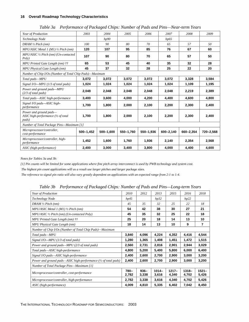
The demand for a higher number of functions on a single chip requires the integration of an increased number of transistors or bits (memory cells) for each product generation. Typically, the number of pads and pins necessary to allow Input/Output (I/O) signals to flow to and from an integrated circuit increases as the number of transistors on a chip increases. (Refer to Tables 3a and b)
Additional power and ground connections to the chip are also necessary to optimize power management and to increase noise immunity. Based upon chip pad-count numbers supplied by the Test ITWG, logic products (MPUs and high-performance ASICs) both approach 4–6K pads over the ITRS period. The MPU products are forecast to increase the total number of pads through this period by nearly 50%, and the ASICs double the maximum number of pads per chip. The two product types also differ significantly in the ratio of power/ground pads. The MPU product pad counts typically have 1:3 signal I/O pads and 2:3 power and ground pads, or two power/ground pads for every signal I/O pad. Unlike MPUs, high-performance ASIC product pad counts typically include one power/ground pad for each signal I/O pad.
16 Overall Roadmap Technology Characteristics
THE INTERNATIONAL TECHNOLOGY ROADMAP FOR SEMICONDUCTORS: 2003
Table 3a Performance of Packaged Chips: Number of Pads and Pins—Near-term Years
Year of Production 2003 2004 2005 2006 2007 2008 2009
Technology Node hp90 hp65
DRAM ½ Pitch (nm) 100 90 80 70 65 57 50
MPU/ASIC Metal 1 (M1) ½ Pitch (nm) 120 107 95 85 76 67 60
MPU/ASIC ½ Pitch (nm) (Un-contacted Poly)
107 90 80 70 65 57 50
MPU Printed Gate Length (nm) †† 65 53 45 40 35 32 28
MPU Physical Gate Length (nm) 45 37 32 28 25 22 20
Number of Chip I/Os (Number of Total Chip Pads)—Maximum
Total pads—MPU 3,072 3,072 3,072 3,072 3,072 3,328 3,584
Signal I/O—MPU (1/3 of total pads) 1,024 1,024 1,024 1,024 1,024 1,109 1,195
Power and ground pads—MPU (2/3 of total pads)
2,048 2,048 2,048 2,048 2,048 2,219 2,389
Total pads—ASIC high-performance 3,400 3,600 4,000 4,200 4,400 4,600 4,800
Signal I/O pads—ASIC high-performance
1,700 1,800 2,000 2,100 2,200 2,300 2,400
Power and ground pads— ASIC high-performance (½ of total pads)
1,700 1,800 2,000 2,100 2,200 2,300 2,400
Number of Total Package Pins—Maximum [1]
Microprocessor/controller, cost-performance
500–1,452 500–1,600 550–1,760 550–1,936 600–2,140 660–2,354 720–2,568
Microprocessor/controller, high-performance
1,452 1,600 1,760 1,936 2,140 2,354 2,568
ASIC (high-performance) 2,400 3,000 3,400 3,800 4,000 4,400 4,600
Notes for Tables 3a and 3b:
[1] Pin counts will be limited for some applications where fine pitch array interconnect is used by PWB technology and system cost.
The highest pin count applications will as a result use larger pitches and larger package sizes.
The reference to signal pin ratio will also vary greatly dependent on applications with an expected range from 2:1 to 1:4.
Table 3b Performance of Packaged Chips: Number of Pads and Pins—Long-term Years
Year of Production 2010 2012 2013 2015 2016 2018
Technology Node hp45 hp32 hp22
DRAM ½ Pitch (nm) 45 35 32 25 22 18
MPU/ASIC Metal 1 (M1) ½ Pitch (nm) 54 42 38 30 27 21
MPU/ASIC ½ Pitch (nm) (Un-contacted Poly) 45 35 32 25 22 18
MPU Printed Gate Length (nm) †† 25 20 18 14 13 10
MPU Physical Gate Length (nm) 18 14 13 10 9 7
Number of Chip I/Os (Number of Total Chip Pads)—Maximum
Total pads—MPU 3,840 4,096 4,224 4,352 4,416 4,544
Signal I/O—MPU (1/3 of total pads) 1,280 1,365 1,408 1,451 1,472 1,515
Power and ground pads—MPU (2/3 of total pads) 2,560 2,731 2,816 2,901 2,944 3,029
Total pads—ASIC high-performance 4,800 5,200 5,400 5,800 6,000 6,400
Signal I/O pads—ASIC high-performance 2,400 2,600 2,700 2,900 3,000 3,200
Power and ground pads—ASIC high-performance (½ of total pads) 2,400 2,600 2,700 2,900 3,000 3,200
Number of Total Package Pins—Maximum [1]
Microprocessor/controller, cost-performance 780–2,782
936–3,338
1014–3,616
1217–4,340
1318–4,702
1521–5,426
Microprocessor/controller, high-performance 2,782 3,338 3,616 4,340 4,702 5,426
ASIC (high-performance) 4,009 4,810 5,335 6,402 7,042 8,450
Overall Roadmap Technology Characteristics 17
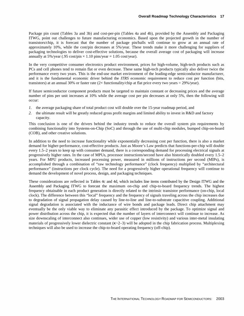
THE INTERNATIONAL TECHNOLOGY ROADMAP FOR SEMICONDUCTORS: 2003
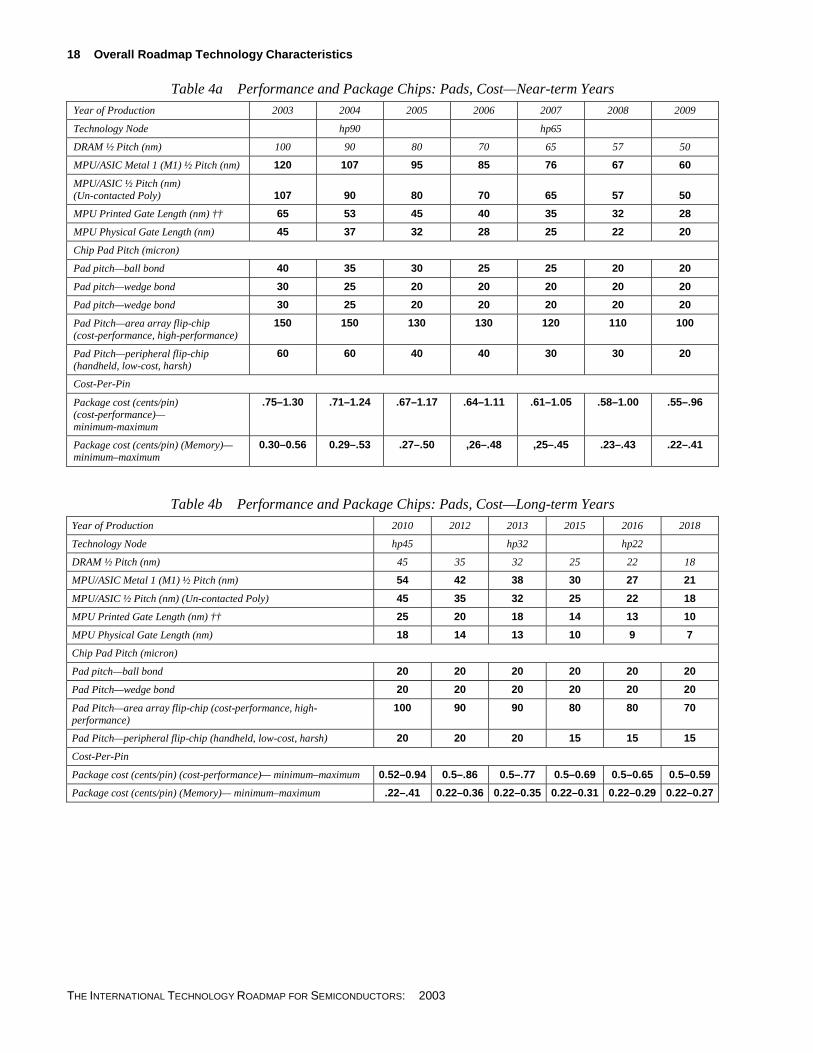
Package pin count (Tables 3a and 3b) and cost-per-pin (Tables 4a and 4b), provided by the Assembly and Packaging ITWG, point out challenges to future manufacturing economics. Based upon the projected growth in the number of transistors/chip, it is forecast that the number of package pin/balls will continue to grow at an annual rate of approximately 10%, while the cost/pin decreases at 5%/year. These trends make it more challenging for suppliers of packaging technologies to deliver cost-effective solutions, because the overall average cost of packaging will increase annually at 5%/year (.95 cost/pin × 1.10 pins/year = 1.05 cost/year).
In the very competitive consumer electronics product environment, prices for high-volume, high-tech products such as PCs and cell phones tend to remain flat or even decrease. These same high-tech products typically also deliver twice the performance every two years. This is the end-use market environment of the leading-edge semiconductor manufacturer, and it is the fundamental economic driver behind the ITRS economic requirement to reduce cost per function (bits, transistors) at an annual 30% or faster rate (2× functionality/chip at flat price every two years = 29%/year).
If future semiconductor component products must be targeted to maintain constant or decreasing prices and the average number of pins per unit increases at 10% while the average cost per pin decreases at only 5%, then the following will occur:
1. the average packaging share of total product cost will double over the 15-year roadmap period, and 2. the ultimate result will be greatly reduced gross profit margins and limited ability to invest in R&D and factory
capacity.
This conclusion is one of the drivers behind the industry trends to reduce the overall system pin requirements by combining functionality into Systems-on-Chip (SoC) and through the use of multi-chip modules, bumped chip-on-board (COB), and other creative solutions.
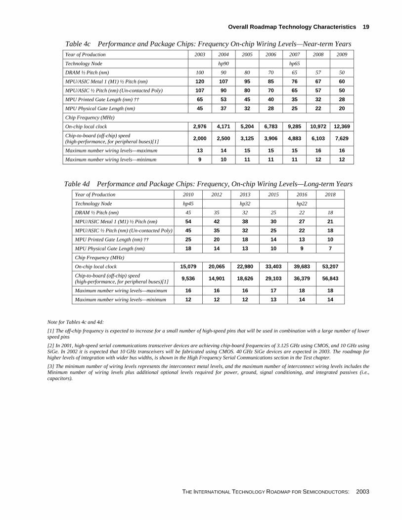
In addition to the need to increase functionality while exponentially decreasing cost per function, there is also a market demand for higher-performance, cost-effective products. Just as Moore’s Law predicts that functions-per-chip will double every 1.5–2 years to keep up with consumer demand, there is a corresponding demand for processing electrical signals at progressively higher rates. In the case of MPUs, processor instructions/second have also historically doubled every 1.5–2 years. For MPU products, increased processing power, measured in millions of instructions per second (MIPs), is accomplished through a combination of “raw technology performance” (clock frequency) multiplied by “architectural performance” (instructions per clock cycle). The need for a progressively higher operational frequency will continue to demand the development of novel process, design, and packaging techniques.
These considerations are reflected in Tables 4c and 4d, which includes line items contributed by the Design ITWG and the Assembly and Packaging ITWG to forecast the maximum on-chip and chip-to-board frequency trends. The highest frequency obtainable in each product generation is directly related to the intrinsic transistor performance (on-chip, local clock). The difference between this “local” frequency and the frequency of signals traveling across the chip increases due to degradation of signal propagation delay caused by line-to-line and line-to-substrate capacitive coupling. Additional signal degradation is associated with the inductance of wire bonds and package leads. Direct chip attachment may eventually be the only viable way to eliminate any parasitic effect introduced by the package. To optimize signal and power distribution across the chip, it is expected that the number of layers of interconnect will continue to increase. As size downscaling of interconnect also continues, wider use of copper (low resistivity) and various inter-metal insulating materials of progressively lower dielectric constant (κ~2–3) will be adopted in the chip fabrication process. Multiplexing techniques will also be used to increase the chip-to-board operating frequency (off-chip).
18 Overall Roadmap Technology Characteristics
THE INTERNATIONAL TECHNOLOGY ROADMAP FOR SEMICONDUCTORS: 2003
Table 4a Performance and Package Chips: Pads, Cost—Near-term Years
Year of Production 2003 2004 2005 2006 2007 2008 2009
Technology Node hp90 hp65
DRAM ½ Pitch (nm) 100 90 80 70 65 57 50
MPU/ASIC Metal 1 (M1) ½ Pitch (nm) 120 107 95 85 76 67 60
MPU/ASIC ½ Pitch (nm) (Un-contacted Poly) 107 90 80 70 65 57 50
MPU Printed Gate Length (nm) †† 65 53 45 40 35 32 28
MPU Physical Gate Length (nm) 45 37 32 28 25 22 20
Chip Pad Pitch (micron)
Pad pitch—ball bond 40 35 30 25 25 20 20
Pad pitch—wedge bond 30 25 20 20 20 20 20
Pad pitch—wedge bond 30 25 20 20 20 20 20
Pad Pitch—area array flip-chip (cost-performance, high-performance)
150 150 130 130 120 110 100
Pad Pitch—peripheral flip-chip (handheld, low-cost, harsh)
60 60 40 40 30 30 20
Cost-Per-Pin
Package cost (cents/pin) (cost-performance)— minimum-maximum
.75–1.30 .71–1.24 .67–1.17 .64–1.11 .61–1.05 .58–1.00 .55–.96
Package cost (cents/pin) (Memory)—minimum–maximum
0.30–0.56 0.29–.53 .27–.50 ,26–.48 ,25–.45 .23–.43 .22–.41
Table 4b Performance and Package Chips: Pads, Cost—Long-term Years
Year of Production 2010 2012 2013 2015 2016 2018
Technology Node hp45 hp32 hp22
DRAM ½ Pitch (nm) 45 35 32 25 22 18
MPU/ASIC Metal 1 (M1) ½ Pitch (nm) 54 42 38 30 27 21
MPU/ASIC ½ Pitch (nm) (Un-contacted Poly) 45 35 32 25 22 18
MPU Printed Gate Length (nm) †† 25 20 18 14 13 10
MPU Physical Gate Length (nm) 18 14 13 10 9 7
Chip Pad Pitch (micron)
Pad pitch—ball bond 20 20 20 20 20 20
Pad Pitch—wedge bond 20 20 20 20 20 20
Pad Pitch—area array flip-chip (cost-performance, high-performance)
100 90 90 80 80 70
Pad Pitch—peripheral flip-chip (handheld, low-cost, harsh) 20 20 20 15 15 15
Cost-Per-Pin
Package cost (cents/pin) (cost-performance)— minimum–maximum 0.52–0.94 0.5–.86 0.5–.77 0.5–0.69 0.5–0.65 0.5–0.59
Package cost (cents/pin) (Memory)— minimum–maximum .22–.41 0.22–0.36 0.22–0.35 0.22–0.31 0.22–0.29 0.22–0.27
Overall Roadmap Technology Characteristics 19
THE INTERNATIONAL TECHNOLOGY ROADMAP FOR SEMICONDUCTORS: 2003
Table 4c Performance and Package Chips: Frequency On-chip Wiring Levels—Near-term Years
Year of Production 2003 2004 2005 2006 2007 2008 2009
Technology Node hp90 hp65
DRAM ½ Pitch (nm) 100 90 80 70 65 57 50
MPU/ASIC Metal 1 (M1) ½ Pitch (nm) 120 107 95 85 76 67 60
MPU/ASIC ½ Pitch (nm) (Un-contacted Poly) 107 90 80 70 65 57 50
MPU Printed Gate Length (nm) †† 65 53 45 40 35 32 28
MPU Physical Gate Length (nm) 45 37 32 28 25 22 20
Chip Frequency (MHz)
On-chip local clock 2,976 4,171 5,204 6,783 9,285 10,972 12,369
Chip-to-board (off-chip) speed (high-performance, for peripheral buses)[1]
2,000 2,500 3,125 3,906 4,883 6,103 7,629
Maximum number wiring levels—maximum 13 14 15 15 15 16 16
Maximum number wiring levels—minimum 9 10 11 11 11 12 12
Table 4d Performance and Package Chips: Frequency, On-chip Wiring Levels—Long-term Years
Year of Production 2010 2012 2013 2015 2016 2018
Technology Node hp45 hp32 hp22
DRAM ½ Pitch (nm) 45 35 32 25 22 18
MPU/ASIC Metal 1 (M1) ½ Pitch (nm) 54 42 38 30 27 21
MPU/ASIC ½ Pitch (nm) (Un-contacted Poly) 45 35 32 25 22 18
MPU Printed Gate Length (nm) †† 25 20 18 14 13 10
MPU Physical Gate Length (nm) 18 14 13 10 9 7
Chip Frequency (MHz)
On-chip local clock 15,079 20,065 22,980 33,403 39,683 53,207
Chip-to-board (off-chip) speed (high-performance, for peripheral buses)[1]
9,536 14,901 18,626 29,103 36,379 56,843
Maximum number wiring levels—maximum 16 16 16 17 18 18
Maximum number wiring levels—minimum 12 12 12 13 14 14
Note for Tables 4c and 4d:
[1] The off-chip frequency is expected to increase for a small number of high-speed pins that will be used in combination with a large number of lower speed pins
[2] In 2001, high-speed serial communications transceiver devices are achieving chip-board frequencies of 3.125 GHz using CMOS, and 10 GHz using SiGe. In 2002 it is expected that 10 GHz transceivers will be fabricated using CMOS. 40 GHz SiGe devices are expected in 2003. The roadmap for higher levels of integration with wider bus widths, is shown in the High Frequency Serial Communications section in the Test chapter.
[3] The minimum number of wiring levels represents the interconnect metal levels, and the maximum number of interconnect wiring levels includes the Minimum number of wiring levels plus additional optional levels required for power, ground, signal conditioning, and integrated passives (i.e., capacitors).
20 Overall Roadmap Technology Characteristics
THE INTERNATIONAL TECHNOLOGY ROADMAP FOR SEMICONDUCTORS: 2003
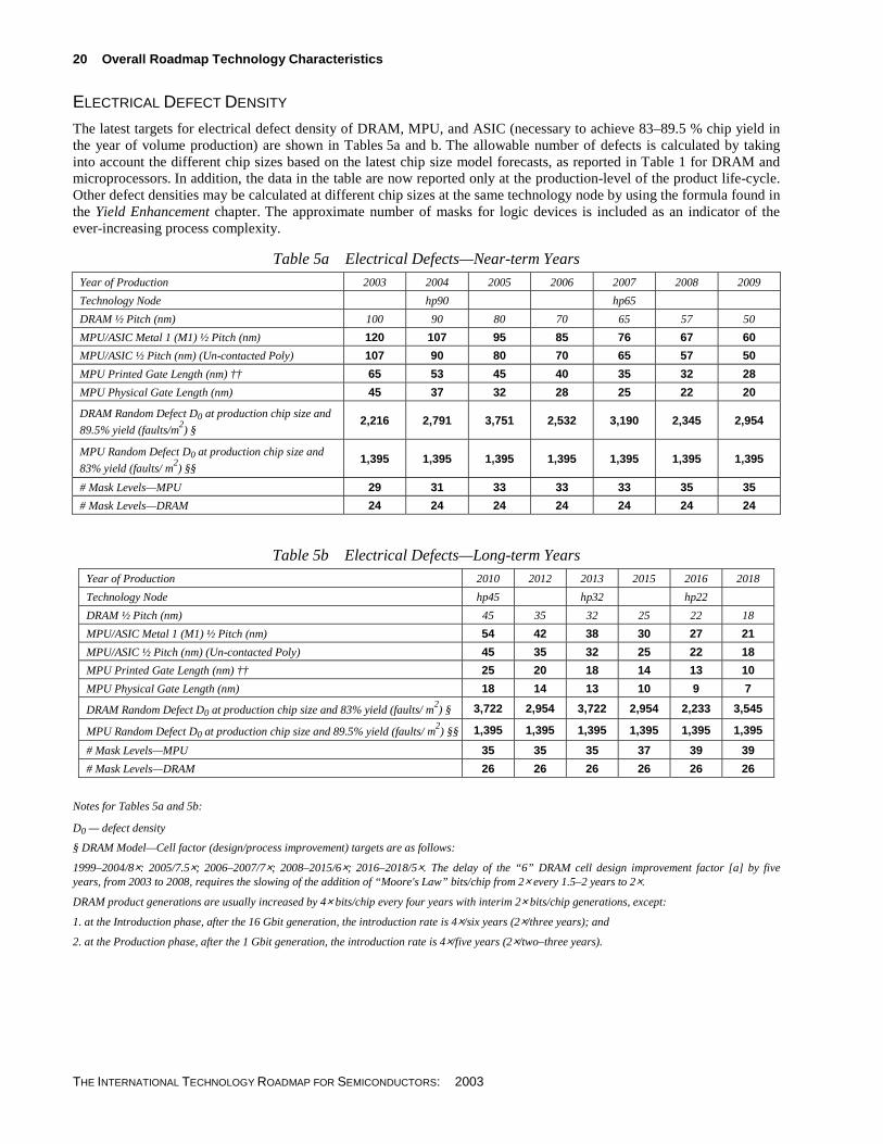
ELECTRICAL DEFECT DENSITY
The latest targets for electrical defect density of DRAM, MPU, and ASIC (necessary to achieve 83–89.5 % chip yield in the year of volume production) are shown in Tables 5a and b. The allowable number of defects is calculated by taking into account the different chip sizes based on the latest chip size model forecasts, as reported in Table 1 for DRAM and microprocessors. In addition, the data in the table are now reported only at the production-level of the product life-cycle. Other defect densities may be calculated at different chip sizes at the same technology node by using the formula found in the Yield Enhancement chapter. The approximate number of masks for logic devices is included as an indicator of the ever-increasing process complexity.
Table 5a Electrical Defects—Near-term Years
Year of Production 2003 2004 2005 2006 2007 2008 2009
Technology Node hp90 hp65
DRAM ½ Pitch (nm) 100 90 80 70 65 57 50
MPU/ASIC Metal 1 (M1) ½ Pitch (nm) 120 107 95 85 76 67 60
MPU/ASIC ½ Pitch (nm) (Un-contacted Poly) 107 90 80 70 65 57 50
MPU Printed Gate Length (nm) †† 65 53 45 40 35 32 28
MPU Physical Gate Length (nm) 45 37 32 28 25 22 20
DRAM Random Defect D0 at production chip size and
89.5% yield (faults/m2) §
2,216 2,791 3,751 2,532 3,190 2,345 2,954
MPU Random Defect D0 at production chip size and
83% yield (faults/ m2) §§
1,395 1,395 1,395 1,395 1,395 1,395 1,395
# Mask Levels—MPU 29 31 33 33 33 35 35
# Mask Levels—DRAM 24 24 24 24 24 24 24
Table 5b Electrical Defects—Long-term Years
Year of Production 2010 2012 2013 2015 2016 2018
Technology Node hp45 hp32 hp22
DRAM ½ Pitch (nm) 45 35 32 25 22 18
MPU/ASIC Metal 1 (M1) ½ Pitch (nm) 54 42 38 30 27 21
MPU/ASIC ½ Pitch (nm) (Un-contacted Poly) 45 35 32 25 22 18
MPU Printed Gate Length (nm) †† 25 20 18 14 13 10
MPU Physical Gate Length (nm) 18 14 13 10 9 7
DRAM Random Defect D0 at production chip size and 83% yield (faults/ m2) § 3,722 2,954 3,722 2,954 2,233 3,545
MPU Random Defect D0 at production chip size and 89.5% yield (faults/ m2) §§ 1,395 1,395 1,395 1,395 1,395 1,395
# Mask Levels—MPU 35 35 35 37 39 39
# Mask Levels—DRAM 26 26 26 26 26 26
Notes for Tables 5a and 5b:
D0 — defect density
§ DRAM Model—Cell factor (design/process improvement) targets are as follows:
1999–2004/8×: 2005/7.5×; 2006–2007/7×; 2008–2015/6×; 2016–2018/5×. The delay of the “6” DRAM cell design improvement factor [a] by five years, from 2003 to 2008, requires the slowing of the addition of “Moore's Law” bits/chip from 2× every 1.5–2 years to 2×.
DRAM product generations are usually increased by 4× bits/chip every four years with interim 2× bits/chip generations, except:
1. at the Introduction phase, after the 16 Gbit generation, the introduction rate is 4×/six years (2×/three years); and
2. at the Production phase, after the 1 Gbit generation, the introduction rate is 4×/five years (2×/two–three years).
Overall Roadmap Technology Characteristics 21
THE INTERNATIONAL TECHNOLOGY ROADMAP FOR SEMICONDUCTORS: 2003
The original 2001 ITRS InTER-generation chip size growth rate was targeted to fit one chip per 572 mm2 field at Introduction and two chips per
572 mm2 field at Production. Due to the delay of the cell area factor reductions, Introduction chip sizes increased, but the new 704 mm
2 maximum
affordable lithography field allows the Introduction chip to double bits per chip every two years through the 16 Gbit generation (660 mm2/2007).
Slowing the “Moore's Law” bits per chip of the Introduction-phase DRAM model to an average of 2× per 2.5 years enables the Introduction DRAMs to remain under the original 572 mm
2 affordable target after 2007. The InTRA-generation chip size shrink model remains at 0.5× every technology node
in-between cell factor reductions, and eventually (ranging from five to six years), the Introduction-phase DRAMs shrink below the 140 mm2 Production-
phase chip size target.
§§ MPU Chip Size Model—Both the cost-performance and high-performance MPUs InTER-generation chip size growth rates are targeted to be flat through 2018 (280 mm
2/cost-performance at introduction; 140 mm
2/cost-performance at production; 310 mm
2/high-performance at production). The
MPU flat chip-size model is made possible by doubling the on-chip functionality every technology node cycle. The InTRA-generation chip size shrink model was 0.5× every two-year technology node through 2001, and is now 0.5× every three-year technology node cycle after 2003.
Refer to the Glossary for definitions of Introduction, Production, InTERgeneration, and InTRAgeneration terms.
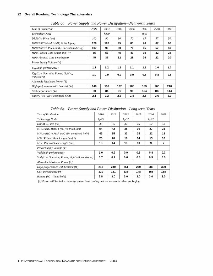
POWER SUPPLY AND POWER DISSIPATION
The reduction of power supply voltage is driven by several factors—reduction of power dissipation, reduced transistor channel length, and reliability of gate dielectrics. As seen in Tables 6a and b, the value of the power supply voltage is now given as a range.
Selection of a specific Vdd value continues to be a part of the analysis undertaken to simultaneously optimize speed and power for an IC, leading to a range of usable power supply voltages in each product generation. Values of Vdd as low as 0.5 volts are not expected to be achieved by high-performance processors until beyond 2018 (versus 2013 in the 2001 ITRS). The lowest Vdd target is now 0.5V in 2016 for the low operating power applications, a lower target than the 0.6V goal in the 2001 ITRS).
Maximum power trends (e.g., for MPUs) are presented in three categories—1) high-performance desktop applications, for which a heat sink on the package is permitted; 2) cost-performance, where economical power management solutions of the highest performance are most important; and 3) portable battery operations (now designated as the “Harsh” application category by the Assembly and Packaging TWG). In all cases, total power consumption continues to increase, despite the use of a lower supply voltage. The increased power consumption is driven by higher chip operating frequencies, the higher interconnect overall capacitance and resistance and the increasing gate leakage of exponentially growing and scaled on-chip transistors.
22 Overall Roadmap Technology Characteristics
THE INTERNATIONAL TECHNOLOGY ROADMAP FOR SEMICONDUCTORS: 2003
Table 6a Power Supply and Power Dissipation—Near-term Years
Year of Production 2003 2004 2005 2006 2007 2008 2009
Technology Node hp90 hp65
DRAM ½ Pitch (nm) 100 90 80 70 65 57 50
MPU/ASIC Metal 1 (M1) ½ Pitch (nm) 120 107 95 85 76 67 60
MPU/ASIC ½ Pitch (nm) (Un-contacted Poly) 107 90 80 70 65 57 50
MPU Printed Gate Length (nm) †† 65 53 45 40 35 32 28
MPU Physical Gate Length (nm) 45 37 32 28 25 22 20
Power Supply Voltage (V)
Vdd (high-performance) 1.2 1.2 1.1 1.1 1.1 1.0 1.0
Vdd (Low Operating Power, high Vdd transistors)
1.0 0.9 0.9 0.9 0.8 0.8 0.8
Allowable Maximum Power [1]
High-performance with heatsink (W) 149 158 167 180 189 200 210
Cost-performance (W) 80 84 91 98 104 109 114
Battery (W)—(low-cost/hand-held) 2.1 2.2 2.3 2.4 2.5 2.6 2.7
Table 6b Power Supply and Power Dissipation—Long-term Years
Year of Production 2010 2012 2013 2015 2016 2018
Technology Node hp45 hp32 hp22
DRAM ½ Pitch (nm) 45 35 32 25 22 18
MPU/ASIC Metal 1 (M1) ½ Pitch (nm) 54 42 38 30 27 21
MPU/ASIC ½ Pitch (nm) (Un-contacted Poly) 45 35 32 25 22 18
MPU Printed Gate Length (nm) †† 25 20 18 14 13 10
MPU Physical Gate Length (nm) 18 14 13 10 9 7
Power Supply Voltage (V)
Vdd (high-performance) 1.0 0.9 0.9 0.8 0.8 0.7
Vdd (Low Operating Power, high Vdd transistors) 0.7 0.7 0.6 0.6 0.5 0.5
Allowable Maximum Power [1]
High-performance with heatsink (W) 218 240 251 270 288 300
Cost-performance (W) 120 131 138 148 158 168
Battery (W)—(hand-held) 2.8 3.0 3.0 3.0 3.0 3.0
[1] Power will be limited more by system level cooling and test constraints than packaging
Overall Roadmap Technology Characteristics 23
THE INTERNATIONAL TECHNOLOGY ROADMAP FOR SEMICONDUCTORS: 2003
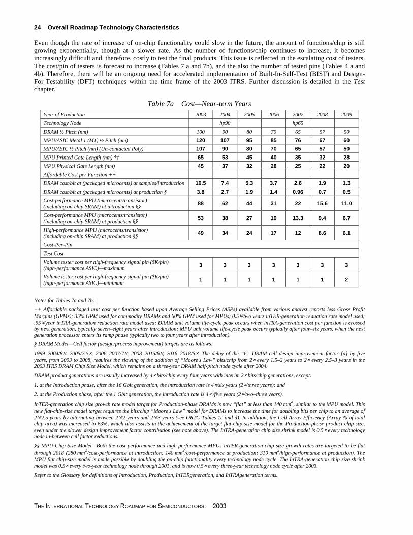
COST
Tables 7a and 7b are dedicated to cost trends. The historical ability to reduce the cost per function by an average 25–30% each year has represented one of the unique features of the semiconductor industry and is a direct consequence of the market pressure to continue to deliver twice the functionality on-chip every 1.5–2 years in an environment of constant or reducing prices. In support of this market cost reduction mandate, a continuously increasing amount of investment is needed for R&D and manufacturing capital. Even on a per-factory basis, the capital cost of manufacturing continues to escalate. Yet, the semiconductor industry has historically delivered two times as many functions per chip every 1.5–2 years with an approximately constant cost per cm2 of silicon. This technological and economic performance is the fundamental engine behind the growth of the semiconductor industry.
However, the customers in today’s challenging economic and competitive market environment continue to be resistant to even “moderate” increases in cost, putting pressure upon the semiconductor industry to slow rate of doubling functions per chip (Moore’s Law) in order to keep chip and unit costs under control. The semiconductor manufacturers had to seek a new model to deliver the same cost-per-function reduction requirements that have fueled industry growth. Consequently, the 1999 ITRS proposed a new model for achieving the required reduction: provide the customer twice the functionality every two years at constant cost targets. The 2001 and 2003 ITRS models both continue to use that model, which results in 29% cost reduction of a function (bit, transistor, etc.). That rate of function cost reduction was achieved historically (prior to 1999) by delivering four times the functionality per chip every three years at 1.4× increase in cost per unit.
The 2003 ITRS DRAM and MPU cost models continue to use the need for that 29% cost-per-function productivity reduction rate as an economic driver of the industry. Therefore, that core cost-per-function trend has been used to set the INTRA-generation trends for the affordable cost/bit and cost/transistor for DRAM and microprocessors, respectively. Extrapolation of historical trends would indicate an “at introduction” affordable cost/bit of 10.5 microcents for 4-Gbit DRAMs in 2003. In addition, the historical trends indicate that, within a DRAM generation, a 45%/year reduction in cost/bit should be expected.1 A corresponding analysis conducted from published data for microprocessors yields similar results.2 Therefore, the 29%/year target for reduction in affordable cost/transistor from generation to generation is also being used in the MPU model, along with the 45%/year reduction rate within the same generation.
The 2003 ITRS retains the original 2001 MPU chip size model. The Design ITWG updated the MPU model in the 2001 ITRS, based upon available data. At that time, the data indicated that logic transistor size is improving only at the rate of the lithography (0.7× linear, 0.5× area reduction every technology node). Therefore in order to keep the MPU chip sizes flat, the number of transistors can be doubled only every technology node. The technology node rate is projected to return to a three-year cycle after 2001, therefore the transistors per MPU chip can double only every three years after 2001.
DRAM memory bit cell design improvements are also continuing to slow, as reflected in the 2003 ITRS DRAM Chip Size Model targets. The “6” design factor, a 25% improvement over the “8” factor, was expected to be implemented in 2003, but has now been delayed five years to 2008. Furthermore the “4” design factor, a 33% improvement over the “6” factor, was changed to “5” in the 2003 ITRS, and delayed from 2011 to 2016. Consequently the target for the cell array efficiency percentage was increased to 63% and the rate of bits per chip was slowed in the future from 2×/two years to 2×/2.5-3 years. These adjustments to the 2003 ITRS DRAM chip size model were required in order to preserve a constant chip size target of less than 140 mm2.
To compensate for slowing DRAM and MPU functions-per-chip, there will be increasing pressure to find alternative productivity enhancements from the equivalent productivity scaling benefits of chip, package, board, and system-level architecture and designs.
1 McClean, William J., ed. Mid-Term 1994: Status and Forecast of the IC Industry. Scottsdale: Integrated Circuit Engineering Corporation, 1994. McClean, William J., ed. Mid-Term 1995: Status and Forecast of the IC Industry. Scottsdale: Integrated Circuit Engineering Corporation, 1995. 2 a) Dataquest Incorporated. x86 Market: Detailed Forecast, Assumptions, and Trends. MCRO–WW–MT–9501. San Jose: Dataquest Incorporated, January 16, 1995. b) Port, Otis; Reinhardt, Andy; McWilliams, Gary; and Brull, Steven V. “The Silicon Age? It's Just Dawning,” Table 1. Business Week, December 9, 1996, 148–152.
24 Overall Roadmap Technology Characteristics
THE INTERNATIONAL TECHNOLOGY ROADMAP FOR SEMICONDUCTORS: 2003
Even though the rate of increase of on-chip functionality could slow in the future, the amount of functions/chip is still growing exponentially, though at a slower rate. As the number of functions/chip continues to increase, it becomes increasingly difficult and, therefore, costly to test the final products. This issue is reflected in the escalating cost of testers. The cost/pin of testers is forecast to increase (Tables 7 a and 7b), and the also the number of tested pins (Tables 4 a and 4b). Therefore, there will be an ongoing need for accelerated implementation of Built-In-Self-Test (BIST) and Design-For-Testability (DFT) techniques within the time frame of the 2003 ITRS. Further discussion is detailed in the Test chapter.
Table 7a Cost—Near-term Years
Year of Production 2003 2004 2005 2006 2007 2008 2009
Technology Node hp90 hp65
DRAM ½ Pitch (nm) 100 90 80 70 65 57 50
MPU/ASIC Metal 1 (M1) ½ Pitch (nm) 120 107 95 85 76 67 60
MPU/ASIC ½ Pitch (nm) (Un-contacted Poly) 107 90 80 70 65 57 50
MPU Printed Gate Length (nm) †† 65 53 45 40 35 32 28
MPU Physical Gate Length (nm) 45 37 32 28 25 22 20
Affordable Cost per Function ++
DRAM cost/bit at (packaged microcents) at samples/introduction 10.5 7.4 5.3 3.7 2.6 1.9 1.3
DRAM cost/bit at (packaged microcents) at production § 3.8 2.7 1.9 1.4 0.96 0.7 0.5
Cost-performance MPU (microcents/transistor) (including on-chip SRAM) at introduction §§
88 62 44 31 22 15.6 11.0
Cost-performance MPU (microcents/transistor) (including on-chip SRAM) at production §§
53 38 27 19 13.3 9.4 6.7
High-performance MPU (microcents/transistor) (including on-chip SRAM) at production §§
49 34 24 17 12 8.6 6.1
Cost-Per-Pin
Test Cost
Volume tester cost per high-frequency signal pin ($K/pin) (high-performance ASIC)—maximum
3 3 3 3 3 3 3
Volume tester cost per high-frequency signal pin ($K/pin) (high-performance ASIC)—minimum
1 1 1 1 1 1 2
Notes for Tables 7a and 7b:
++ Affordable packaged unit cost per function based upon Average Selling Prices (ASPs) available from various analyst reports less Gross Profit Margins (GPMs); 35% GPM used for commodity DRAMs and 60% GPM used for MPUs; 0.5×/two years inTER-generation reduction rate model used; .55×/year inTRA-generation reduction rate model used; DRAM unit volume life-cycle peak occurs when inTRA-generation cost per function is crossed by next generation, typically seven–eight years after introduction; MPU unit volume life-cycle peak occurs typically after four–six years, when the next generation processor enters its ramp phase (typically two to four years after introduction).
§ DRAM Model—Cell factor (design/process improvement) targets are as follows:
1999–2004/8×: 2005/7.5×; 2006–2007/7×; 2008–2015/6×; 2016–2018/5×. The delay of the “6” DRAM cell design improvement factor [a] by five years, from 2003 to 2008, requires the slowing of the addition of “Moore's Law” bits/chip from 2× every 1.5–2 years to 2× every 2.5–3 years in the 2003 ITRS DRAM Chip Size Model, which remains on a three-year DRAM half-pitch node cycle after 2004.
DRAM product generations are usually increased by 4× bits/chip every four years with interim 2× bits/chip generations, except:
1. at the Introduction phase, after the 16 Gbit generation, the introduction rate is 4×/six years (2×/three years); and
2. at the Production phase, after the 1 Gbit generation, the introduction rate is 4× /five years (2×/two–three years).
InTER-generation chip size growth rate model target for Production-phase DRAMs is now “flat” at less than 140 mm2, similar to the MPU model. This
new flat-chip-size model target requires the bits/chip “Moore's Law” model for DRAMs to increase the time for doubling bits per chip to an average of 2×/2.5 years by alternating between 2×/2 years and 2×/3 years (see ORTC Tables 1c and d). In addition, the Cell Array Efficiency (Array % of total chip area) was increased to 63%, which also assists in the achievement of the target flat-chip-size model for the Production-phase product chip size, even under the slower design improvement factor contribution (see note above). The InTRA-generation chip size shrink model is 0.5× every technology node in-between cell factor reductions.
§§ MPU Chip Size Model—Both the cost-performance and high-performance MPUs InTER-generation chip size growth rates are targeted to be flat through 2018 (280 mm
2/cost-performance at introduction; 140 mm
2/cost-performance at production; 310 mm
2/high-performance at production). The
MPU flat chip-size model is made possible by doubling the on-chip functionality every technology node cycle. The InTRA-generation chip size shrink model was 0.5× every two-year technology node through 2001, and is now 0.5× every three-year technology node cycle after 2003.
Refer to the Glossary for definitions of Introduction, Production, InTERgeneration, and InTRAgeneration terms.
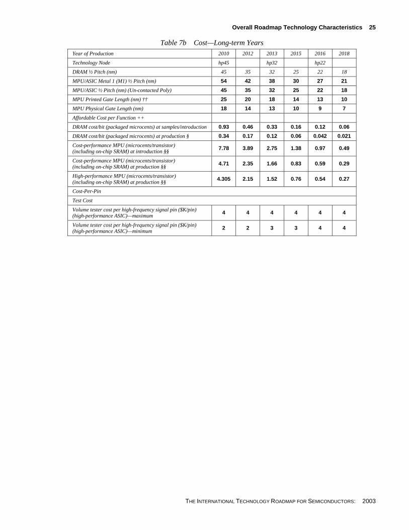
Overall Roadmap Technology Characteristics 25
THE INTERNATIONAL TECHNOLOGY ROADMAP FOR SEMICONDUCTORS: 2003
Table 7b Cost—Long-term Years
Year of Production 2010 2012 2013 2015 2016 2018
Technology Node hp45 hp32 hp22
DRAM ½ Pitch (nm) 45 35 32 25 22 18
MPU/ASIC Metal 1 (M1) ½ Pitch (nm) 54 42 38 30 27 21
MPU/ASIC ½ Pitch (nm) (Un-contacted Poly) 45 35 32 25 22 18
MPU Printed Gate Length (nm) †† 25 20 18 14 13 10
MPU Physical Gate Length (nm) 18 14 13 10 9 7
Affordable Cost per Function ++
DRAM cost/bit (packaged microcents) at samples/introduction 0.93 0.46 0.33 0.16 0.12 0.06
DRAM cost/bit (packaged microcents) at production § 0.34 0.17 0.12 0.06 0.042 0.021
Cost-performance MPU (microcents/transistor) (including on-chip SRAM) at introduction §§
7.78 3.89 2.75 1.38 0.97 0.49
Cost-performance MPU (microcents/transistor) (including on-chip SRAM) at production §§
4.71 2.35 1.66 0.83 0.59 0.29
High-performance MPU (microcents/transistor) (including on-chip SRAM) at production §§
4.305 2.15 1.52 0.76 0.54 0.27
Cost-Per-Pin
Test Cost
Volume tester cost per high-frequency signal pin ($K/pin) (high-performance ASIC)—maximum
4 4 4 4 4 4
Volume tester cost per high-frequency signal pin ($K/pin) (high-performance ASIC)—minimum
2 2 3 3 4 4
26 Glossary
THE INTERNATIONAL TECHNOLOGY ROADMAP FOR SEMICONDUCTORS: 2003
GLOSSARY KEY ROADMAP TECHNOLOGY CHARACTERISTICS TERMINOLOGY (WITH OBSERVATIONS AND ANALYSIS)
CHARACTERISTICS OF MAJOR MARKETS Technology Node—The minimum half-pitch of custom-layout (i.e., with staggered contacts/vias) metal interconnect is most representative of the process capability enabling high-density (low cost/function) integrated circuits and is selected to define an ITRS Technology Node. For each Node, this defining metal half-pitch is taken from whatever product has the minimum value. Historically, DRAMs have had leadership on metal pitch, but this could potentially shift to another product in the future.
Other parameters are also important for characterizing IC technology. For example, in the case of microprocessors (MPUs), physical bottom gate length is most representative of the leading-edge technology level required for maximum performance. Each technology node step represents the creation of significant technology progress in metal half-pitch —approximately 70% of the preceding node, 50% of two preceding nodes.
Example: DRAM half pitches of 180 nm, 130 nm, 90 nm, 65 nm, 45 nm, 32 nm, and 22 nm.
For cost reasons, high-volume, low-cost ASIC gate-length requirements will typically match DRAM half-pitch targets, but the low-volume leading-edge high-performance ASIC gate-length requirements will track closely with MPUs.
An official 2003 ITRS metal half-pitch node indicator, “hpXX,” has been added to differentiate the ITRS definition from commercial technology generation numbers .
Moore’s Law—An historical observation by Intel executive, Gordon Moore, that the market demand (and semiconductor industry response) for functionality per chip (bits, transistors) doubles every 1.5 to 2 years. He also observed that MPU performance [clock frequency (MHz) × instructions per clock = millions of instructions per second (MIPS)] also doubles every 1.5 to 2 years. Although viewed by some as a “self-fulfilling” prophecy, “Moore’s Law” has been a consistent macro trend and key indicator of successful leading-edge semiconductor products and companies for the past 30 years.
Cost-per-Function Manufacturing Productivity Improvement Driver—In addition to Moore’s Law, there is a historically-based “corollary” to the “law,” which suggests that to be competitive manufacturing productivity improvements must also enable the cost-per-function (microcents per bit or transistor) to decrease by -29% per year. Historically, when functionality doubled every 1.5 years, then cost-per-chip (packaged unit) could double every six years and still meet the cost-per-function reduction requirement. If functionality doubles only every three years, as suggested by consensus DRAM and MPU models of the 2003 ITRS, then the manufacturing cost per chip (packaged unit) must remain flat.
Affordable Packaged Unit Cost/Function—Final cost in microcents of the cost of a tested and packaged chip divided by Functions/Chip. Affordable costs are calculated from historical trends of affordable average selling prices [gross annual revenues of a specific product generation divided by the annual unit shipments] less an estimated gross profit margin of approximately 35% for DRAMs and 60% for MPUs. The affordability per function is a guideline of future market “tops-down” needs, and as such, was generated independently from the chip size and function density. Affordability requirements are expected to be achieved through combinations of—1) increased density and smaller chip sizes from technology and design improvements; 2) increasing wafer diameters; 3) decreasing equipment cost-of-ownership; 4) increasing equipment overall equipment effectiveness; 5) reduced package and test costs; 6) improved design tool productivity; and 7) enhanced product architecture and integration.
DRAM Generation at (product generation life-cycle level)—The anticipated bits/chip of the DRAM product generation introduced in a given year, manufacturing technology capability, and life-cycle maturity (Demonstration-level, Introduction-level, Production-level, Ramp-level, Peak).
MPU Generation at (product generation life-cycle level)—The generic processor generation identifier for the anticipated Microprocessor Unit (MPU) product generation functionality (logic plus SRAM transistors per chip) introduced in a given year, manufacturing technology capability, and life-cycle maturity (Introduction-level, Production-level, Ramp-level, Peak).
Glossary 27
THE INTERNATIONAL TECHNOLOGY ROADMAP FOR SEMICONDUCTORS: 2003
Cost-Performance MPU—MPU product optimized for maximum performance and the lowest cost by limiting the amount of on-chip SRAM level-two (L2) cache (example 1Mbytes/2001). Logic functionality and L2 cache typically double every three-year generation.
High-performance MPU—MPU product optimized for maximum system performance by combining a single or multiple CPU cores (example two cores at 25Mt cores in 2001) with a large (example 4Mbyte/2001) level-two (L2) SRAM. Logic functionality and L2 cache typically double every three-year technology generation by doubling the number of on-chip CPU cores and associated memory.
Product inTER-generation—Product generation-to-generation targets for periodically doubling the on-chip functionality at an affordable chip size. The targets are set to maintain Moore’s Law (2×/two years) while preserving economical manufacturability (flat chip size and constant manufacturing cost per unit). This doubling every two years at a constant cost assures that the cost/function reduction rate (inverse productivity improvement) is -29% per year (the target historical rate of reduction). In order to double the on-chip functionality every two years, when technology-node scaling (.7× linear, .5× area) is every three years, an additional device/process design improvement of .8× per two years must be achieved. This requirement represents a design-related (cell-area-factor) area-reduction improvement of at least -11% per year, and this design-related productivity improvement is in addition to the basic lithography-based area reduction of -21% per year (three-year node cycle).
The present 2003 ITRS consensus target for the rate of increase of DRAM bits/chip has increased from 2× bits/chip every two years to 2×/chip every two and half years average. This slower bits/chip growth is required due to the new consensus 2003 ITRS forecast of cell-area-factor improvement of only negative 4–6% per year on average rather than the 2001 ITRS target of -7% per year average. This results in an average DRAM inTER-generation approximately flat chip-size growth. Presently, the MPU transistor area is shrinking only at lithography-based rate (virtually no design-related improvement). Therefore, the 2003 ITRS MPU inTER-generation functionality model target is 2× transistors/chip every technology node, in order maintain a flat chip size growth throughout the roadmap period.
Product inTRA-generation—Chip size shrink trend within a given constant functions-per-chip product generation. The 2003 ITRS consensus-based model targets reduce chip size (by shrinks and “cut-downs”) utilizing the latest available manufacturing and design technology at every point through the roadmap. The ITRS targets for both DRAM and MPU reduce chip size within a generation by minus 50% per technology node.
Year of Demonstration—Year in which the leading chip manufacturer supplies an operational sample of a product as a demonstration of design and/or technology node processing feasibility and prowess. A typical venue for the demonstration is a major semiconductor industry conference, such as the International Solid State Circuits Conference (ISSCC) held by the Institute of Electrical and Electronic Engineers (IEEE). Demonstration samples are typically manufactured with early development or demonstration- level manufacturing tools and processes. Historically, DRAM products have been demonstrated at 4× bits-per-chip every four years at the leading-edge process technology node, typically two–three years in advance of actual market introduction. DRAM demonstration chip sizes have doubled every eight years, requiring an increasing number of shrinks and delay before market introduction is economically feasible. Frequently, chip sizes are larger than the field sizes available from lithography equipment, and must be “stitched” together via multiple-exposure techniques that are feasible only for very small quantities of laboratory samples. Example: 1997/ISSCC/1Gb DRAM, versus ITRS 1Gb 1999 Introduction-level, 2003 Production-level targets.
Year of INTRODUCTION—Year in which the leading chip manufacturer supplies small quantities of engineering samples (<1K). These are provided to key customers for early evaluation, and are manufactured with qualified production tooling and processes. To balance market timeliness and economical manufacturing, products will be introduced at 2× functionality per chip every two years (every technology node, in the case of MPUs). In addition, manufacturers will delay production until a chip-size shrink or “cut-down” level is achieved which limits the inTER-generation chip-size growth to be flat.
Year of PRODUCTION—Year in which at least one leading chip manufacturer begins shipping volume quantities (initially, at least 10K/month) of product manufactured with customer product qualified* production tooling and processes and is followed within three months by a second manufacturer. (*Note: Start of actual volume production ramp may vary between one to twelve months depending upon the length of the customer product qualification). As demand increases for the leading-edge performance and shrink products, the tooling and processes are being quickly “copied” into multiple modules of manufacturing capacity.
For high-demand products, volume production typically continues to ramp to fab design capacity within twelve months. Alpha-level manufacturing tools and research technology papers are typically delivered 24–36 months prior to volume
28 Glossary
THE INTERNATIONAL TECHNOLOGY ROADMAP FOR SEMICONDUCTORS: 2003
production ramp. Beta-level tools are typically delivered 12-24 months prior to ramp, along with papers at industry conferences. The beta-level tools are made production-level in pilot-line fabs, which must be ready 12–24 months prior to Production Ramp “Time Zero” [see Figure 2 in the Executive Summary] to allow for full customer product qualification. The production-level pilot line fabs may also run low volumes of product that is often used for customer sampling and early qualification prior to volume production ramp. Medium-volume production-level DRAMs will be in production concurrently with low-volume introduction-level DRAMs, and also concurrently with very-high-volume, shrunken, previous-generation DRAMs (example: 2003: 1Gb/production, 4G/introduction, plus 512Mb/256Mb/128Mb/64Mb high-volume). Similarly, high-volume cost-performance MPUs are in production concurrently with their lower-volume, large-chip, high-performance MPU counterparts, and also with very-high volume shrinks of previous generations.
Functions/Chip—The number of bits (DRAMs) or logic transistors (MPUs/ASICs) that can be cost-effectively manufactured on a single monolithic chip at the available technology level. Logic functionality (transistors per chip) include both SRAM and gate-function logic transistors. DRAM functionality (bits per chip) is based only on the bits (after repair) on a single monolithic chip.
Chip Size (mm2)—The typical area of the monolithic memory and logic chip that can be affordably manufactured in a
given year based upon the best available leading-edge design and manufacturing process. (Estimates are projected based upon historical data trends and the ITRS consensus models).
Functions/cm2—The density of functions in a given square centimeter = Functions/Chip on a single monolithic chip
divided by the Chip Size. This is an average of the density of all of the functionality on the chip, including pad area and wafer scribe area. In the case of DRAM, it includes the average of the high-density cell array and the less-dense peripheral drive circuitry. In the case of the MPU products, it includes the average of the high-density SRAM and the less-dense random logic. In the case of ASIC, it will include high-density embedded memory arrays, averaged with less dense array logic gates and functional cores. In the 2003 ITRS, the typical high-performance ASIC design is assumed to have the same average density as the high-performance MPUs, which are mostly SRAM transistors.
DRAM Cell Array Area Percentage—The maximum practical percentage of the total DRAM chip area that the cell array can occupy at the various stages of the generation life cycle. At the introduction chip size targets, this percentage must be typically less than 70% to allow space for the peripheral circuitry, pads, and wafer scribe area. Since the pads and scribe area do not scale with lithography, the maximum cell array percentage is reduced in other inTRA-generation shrink levels (typically less than 63% at the production level, and less than 50–55% for smaller previous generation shrunk die at the high-volume ramp level).
DRAM Cell Area (µm2)—The area (C) occupied by the DRAM memory bit cell, expressed as multiplication of a specified
ITRS-consensus cell area factor target (A) times the square of the minimum half-pitch feature (f) size, that is: C = Af2. To calculate the chip size, the cell area must be divided by the array efficiency, a factor (E) that is statistically derived from historical DRAM chip analysis data. Thus an average cell area (CAVE) can be calculated, which is burdened by the overhead of the drivers, I/O, bus lines, and pad area. The formula is: CAVE = C/E.
The total chip area can then be calculated by multiplying the total number of bits/chip times the CAVE.
Example: 1999: A=8; square of the half-pitch, f2= (180 nm)2=.032 µm2; cell area, C=Af2=0.26 µm2; for 1 Gb introduction-level DRAM with a cell efficiency of E=70% of total chip area, the CAVE =C/E=0.37 µm2; therefore, the 1 Gb Chip Size Area=230 bits * 0.37e-6 mm2/bit = 397 mm2.
DRAM Cell Area Factor—A number (A) that expresses the DRAM cell area (C) as a multiple of equivalent square half-pitch (f) units. Typically, the cell factor is expressed by equivalent aspect ratios of the half-pitch units (2×4=8, 2×3=6, 2×2=4, 1.6×1.6=2.5, etc.).
SRAM Cell Area Factor—Similar to the DRAM area factor, only applied to a 6-transistor (6t) logic-technology latch-type memory cell. The number expresses the SRAM 6t cell area as a multiple of equivalent square technology-node half-pitch (f) units. Typically, the cell factor of the SRAM 6t cell is 16–25 times greater than a DRAM memory cell area factor.
Logic Gate Cell Area Factor—Similar to the DRAM and SRAM cell area factors, only applied to a typical 4-transistor (4t) logic gate. The number expresses the logic 4t gate area as a multiple of equivalent square technology-node half-pitch (f) units. Typically, the cell factor of the logic 4t gate is 2.5–3 times greater than an SRAM 6t cell area factor, and 40–80 times greater than a DRAM memory cell area factor.
Usable Transistors/cm2 (High-performance ASIC, Auto Layout)—Number of transistors per cm2 designed by automated layout tools for highly differentiated applications produced in low volumes. High-performance, leading-edge, embedded-array ASICs include both on-chip array logic cells, as well as dense functional cells (MPU, I/O, SRAM, etc). Density

Glossary 29
THE INTERNATIONAL TECHNOLOGY ROADMAP FOR SEMICONDUCTORS: 2003
calculations include the connected (useable) transistors of the array logic cells, in addition to all of the transistors in the dense functional cells. The largest high-performance ASIC designs will fill the available production lithography field.
CHIP AND PACKAGE—PHYSICAL AND ELECTRICAL ATTRIBUTES Number of Chip I/Os–Total (Array) Pads—The maximum number of chip signal I/O pads plus power and ground pads permanently connected to package plane for functional or test purposes, or to provide power/ground contacts (including signal conditioning). These include any direct chip-to-chip interconnections or direct chip attach connections to the board (Package plane is defined as any interconnect plane, leadframe, or other wiring technology inside a package, i.e., any wiring that is not on the chip or on the board.). MPUs typically have a ratio of signal I/O pads to power/ground pads of 1:2, whereas the high-performance ASIC ratio is typically 1:1.
Number of Chip I/Os–Total (Peripheral) Pads—The maximum number of chip signal I/O plus power and ground pads for products with contacts only around the edge of a chip.
Pad Pitch—The distance, center-to-center, between pads, whether on the peripheral edge of a chip, or in an array of pads across the chip.
Number of Package Pins/Balls—The number of pins or solder balls presented by the package for connection to the board (may be fewer than the number of chip-to-package pads because of internal power and ground planes on the package plane or multiple chips per package).
Package Cost (Cost-performance)—Cost of package envelope and external I/O connections (pins/balls) in cents/pin.
CHIP FREQUENCY (MHZ) On-Chip, Local Clock, High-performance—On-chip clock frequency of high-performance, lower volume microprocessors in localized portions of the chip.
Chip-To-Board (Off-chip) Speed (High-performance, Peripheral Buses)—Maximum signal I/O frequency to board peripheral buses of high and low volume logic devices.
OTHER ATTRIBUTES Lithographic Field Size (mm2)—Maximum single step or step-and-scan exposure area of a lithographic tool at the given technology node. The specification represents the minimum specification that a semiconductor manufacturer might specify for a given technology node. The maximum field size may be specified higher than the ORTC target values, and the final exposure area may be achieved by various combinations of exposure width and scan length.
Maximum Number of Wiring Levels—On-chip interconnect levels including local interconnect, local and global routing, power and ground connections, and clock distribution.
FABRICATION ATTRIBUTES AND METHODS
Electrical D0 Defect Density (d/m–2
)—Number of electrically significant defects per square meter at the given technology node, production life-cycle year, and target probe yield.
Minimum Mask Count—Number of masking levels for mature production process flow with maximum wiring level (Logic).
MAXIMUM SUBSTRATE DIAMETER (MM) Bulk or Epitaxial or Silicon-on-Insulator Wafer—Silicon wafer diameter used in volume quantities by mainstream IC suppliers. The ITRS timing targets, contributed by the Factory Integration ITWG, are based on the first 20K wafer-starts-per-month manufacturing facility.

30 Glossary
THE INTERNATIONAL TECHNOLOGY ROADMAP FOR SEMICONDUCTORS: 2003
ELECTRICAL DESIGN AND TEST METRICS
POWER SUPPLY VOLTAGE (V)
Minimum Logic Vdd—Nominal operating voltage of chips from power source for operation at design requirements.
Maximum Power High-performance with Heat Sink (W)—Maximum total power dissipated in high-performance chips with an external heat sink.
Battery (W)—Maximum total power/chip dissipated in battery operated chips.
DESIGN AND TEST Volume Tester Cost/Pin ($K/pin)—Cost of functional (chip sort) test in high volume applications divided by number of package pins.