Embed Size (px)
Citation preview

332:479 Concepts in VLSIDesign
Lecture 6 CMOS Transistor Theory
David Harris and Michael Bushnell
Harvey Mudd College and Rutgers UniversitySpring 2004
Concepts in VLSI Des. Lec. 6 Slide 212/4/2009
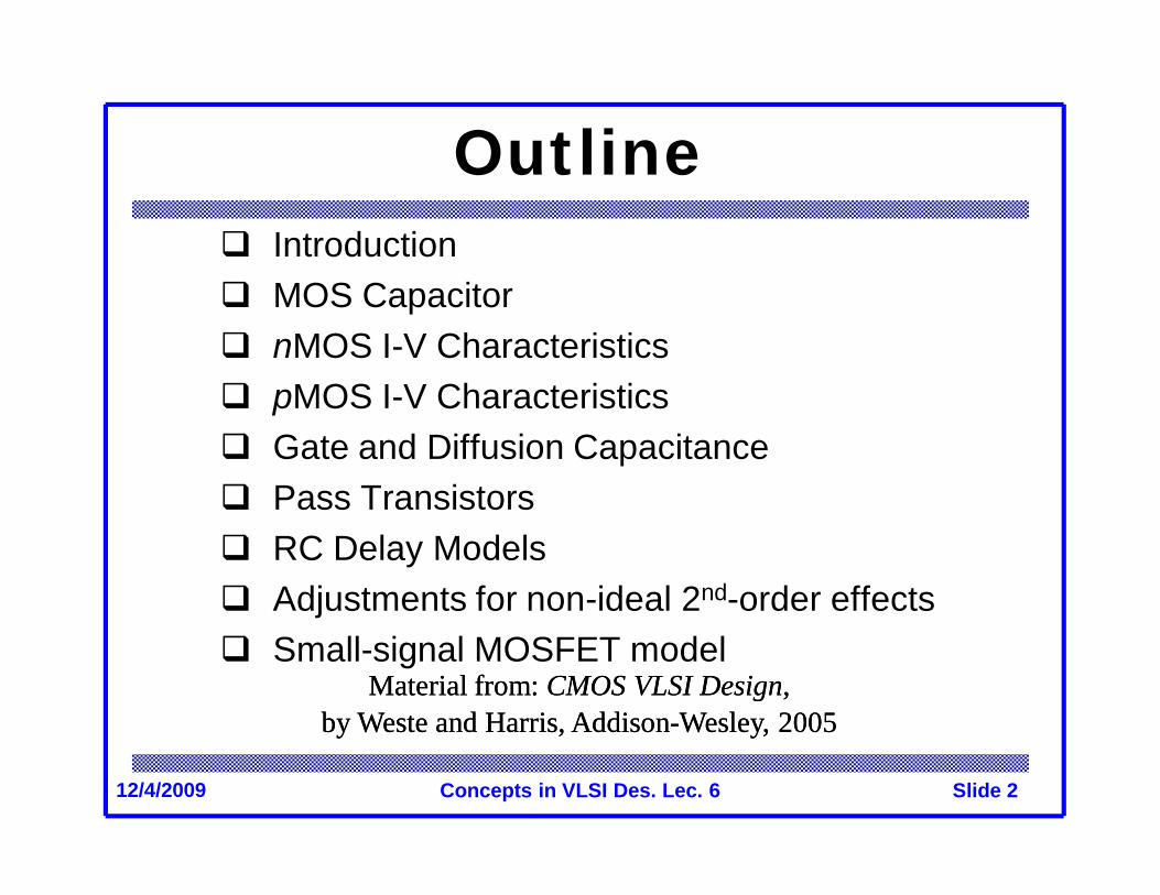
Outline Introduction MOS Capacitor nMOS I-V Characteristics pMOS I-V Characteristics Gate and Diffusion Capacitance Pass Transistors RC Delay Models Adjustments for non-ideal 2nd-order effects Small-signal MOSFET model
Material from:Material from: CMOS VLSI DesignCMOS VLSI Design,,by Weste and Harris, Addisonby Weste and Harris, Addison--Wesley, 2005Wesley, 2005

Concepts in VLSI Des. Lec. 6 Slide 312/4/2009
Introduction So far, we have treated transistors as ideal switches An ON transistor passes a finite amount of current
– Depends on terminal voltages– Derive current-voltage (I-V) relationships
Transistor gate, source, drain all have capacitance– I = C (V/t) -> t = (C/I) V– Capacitance and current determine speed
Also explore what a “degraded level” really means

Concepts in VLSI Des. Lec. 6 Slide 412/4/2009
MOS CharacteristicsMOS – majority carrier device Carriers: e-- in nMOS, holes in pMOS Vt – channel threshold voltage (cuts off for
voltages < Vt)

Concepts in VLSI Des. Lec. 6 Slide 512/4/2009
nMOS Enhancement Transistor
Moderately doped p type Si substrate 2 Heavily doped n+ regions
Concepts in VLSI Des. Lec. 6 Slide 612/4/2009
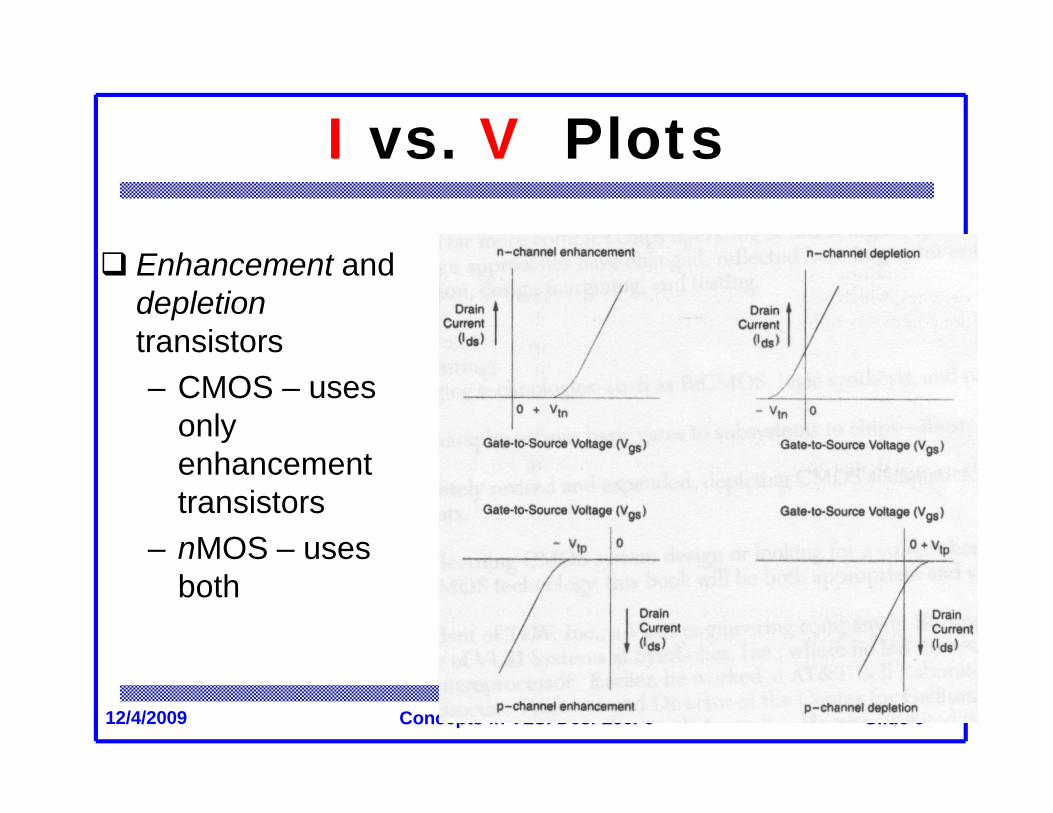
I vs. V Plots
Enhancement and depletiontransistors– CMOS – uses
only enhancement transistors
– nMOS – uses both
Concepts in VLSI Des. Lec. 6 Slide 712/4/2009
Materials and Dopants
SiO2 – low loss, high dielectric strength – High gate fields are possible
n type impurities: P, As, Sb p type impurities: B, Al, Ga, In

Concepts in VLSI Des. Lec. 6 Slide 812/4/2009
Bipolar vs. MOS Bipolar – p-n junction – metallurgicalMOS
– Inversion layer / substrate junction field-induced– Voltage-controlled switch, conducts when Vgs Vt
– e-- swept along channel when Vds > 0 by horizontal component ofE
– Pinch-off – conduction by e–- drift mechanism caused by positive drain voltage
– Pinched-off channel voltage: Vgs – Vt (saturated)– Reverse-biased p-n junction insulates from the substrate

Concepts in VLSI Des. Lec. 6 Slide 912/4/2009
JFET vs. FET Transistors Junction FET (JFET) – channel is deep in
semiconductorMOSFET – For given Vds & Vgs, Ids controlled by:
– Distance between source & drain L– Channel width W– Vt– Gate oxide thickness tox– gate oxide– Carrier mobility

Concepts in VLSI Des. Lec. 6 Slide 1012/4/2009
JFET Transistor

Concepts in VLSI Des. Lec. 6 Slide 1112/4/2009
MOS Capacitor Gate and body form MOS capacitor Operating modes
– Accumulation– Depletion– Inversion
polysilicon gate
(a)
silicon dioxide insulator
p-type body+-
Vg < 0
(b)
+-
0 < Vg < Vt
depletion region
(c)
+-
Vg > Vt
depletion regioninversion region

Concepts in VLSI Des. Lec. 6 Slide 1212/4/2009
Terminal Voltages Mode of operation depends on Vg, Vd, Vs
– Vgs = Vg – Vs
– Vgd = Vg – Vd
– Vds = Vd – Vs = Vgs - Vgd
Source and drain are symmetric diffusion terminals– By convention, source is terminal at lower voltage– Hence Vds 0
nMOS body is grounded. First assume source is 0 too. Three regions of operation
– Cutoff– Linear– Saturation
Vg
Vs Vd
VgdVgs
Vds+-
+
-
+
-

Concepts in VLSI Des. Lec. 6 Slide 1312/4/2009
nMOS Cutoff No channel Ids = 0
+-
Vgs = 0
n+ n+
+-
Vgd
p-type body
b
g
s d

Concepts in VLSI Des. Lec. 6 Slide 1412/4/2009
nMOS Linear Channel forms Current flows from d to
s – e- from s to d
Ids increases with Vds
Similar to linear resistor At drain end of channel,
only difference between gate & drain voltages effective for channel creation
+-
Vgs > Vt
n+ n+
+-
Vgd = Vgs
+-
Vgs > Vt
n+ n+
+-
Vgs > Vgd > Vt
Vds = 0
0 < Vds < Vgs-Vt
p-type body
p-type body
b
g
s d
b
g
s d Ids

Concepts in VLSI Des. Lec. 6 Slide 1512/4/2009
nMOS Saturation Channel pinches off Ids independent of Vds
We say current saturates Similar to current source
+-
Vgs > Vt
n+ n+
+-
Vgd < Vt
Vds > Vgs-Vt
p-type bodyb
g
s d Ids

Concepts in VLSI Des. Lec. 6 Slide 1612/4/2009
I-V Characteristics In Linear region, Ids depends on
– How much charge is in the channel?– How fast is the charge moving?

Concepts in VLSI Des. Lec. 6 Slide 1712/4/2009
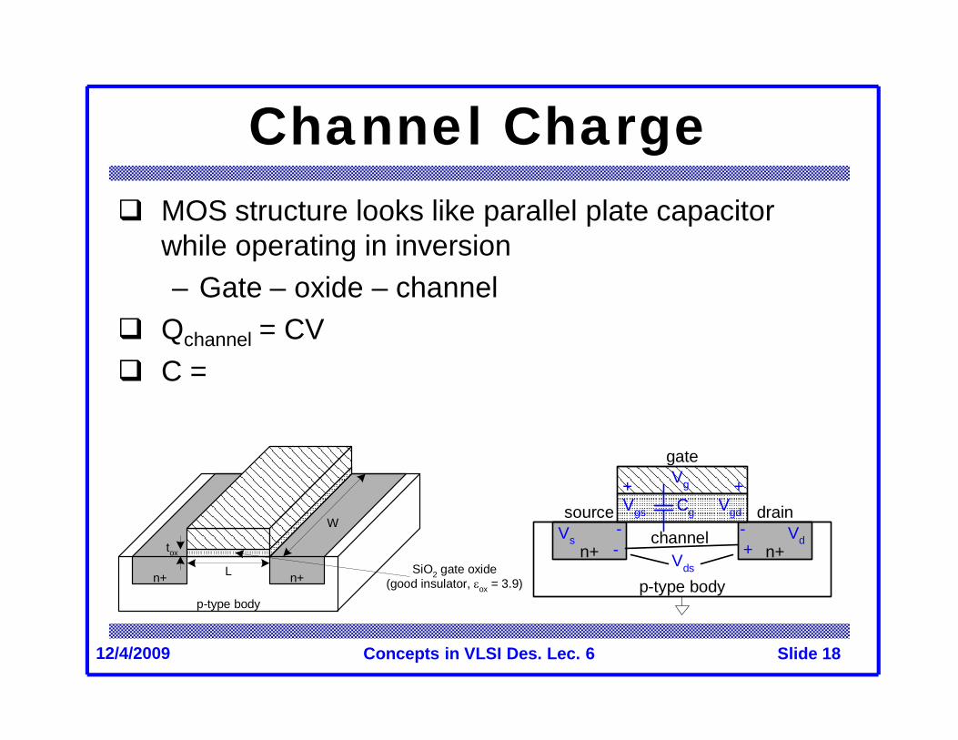
Channel Charge MOS structure looks like parallel plate capacitor
while operating in inversion– Gate – oxide – channel
Qchannel =
n+ n+
p-type body
+
Vgd
gate
+ +source
-
Vgs
-drain
Vds
channel-
Vg
Vs Vd
Cg
n+ n+
p-type body
W
L
tox
SiO2 gate oxide(good insulator, ox = 3.9)
polysilicongate
Concepts in VLSI Des. Lec. 6 Slide 1812/4/2009
Channel Charge MOS structure looks like parallel plate capacitor
while operating in inversion– Gate – oxide – channel
Qchannel = CV C =
n+ n+
p-type body
+
Vgd
gate
+ +source
-
Vgs
-drain
Vds
channel-
Vg
Vs Vd
Cg
n+ n+
p-type body
W
L
tox
SiO2 gate oxide(good insulator, ox = 3.9)
polysilicongate
Concepts in VLSI Des. Lec. 6 Slide 1912/4/2009
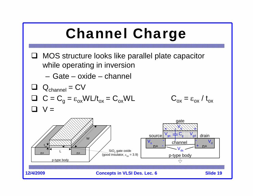
Channel Charge MOS structure looks like parallel plate capacitor
while operating in inversion– Gate – oxide – channel
Qchannel = CV C = Cg = oxWL/tox = CoxWL V =
n+ n+
p-type body
+
Vgd
gate
+ +source
-
Vgs
-drain
Vds
channel-
Vg
Vs Vd
Cg
n+ n+
p-type body
W
L
tox
SiO2 gate oxide(good insulator, ox = 3.9)
polysilicongate
Cox = ox / tox

Concepts in VLSI Des. Lec. 6 Slide 2012/4/2009
Channel Charge MOS structure looks like parallel plate capacitor
while operating in inversion– Gate – oxide – channel
Qchannel = CV C = Cg = oxWL/tox = CoxWL V = Vgc – Vt = (Vgs – Vds/2) – Vt
n+ n+
p-type body
+
Vgd
gate
+ +source
-
Vgs
-drain
Vds
channel-
Vg
Vs Vd
Cg
n+ n+
p-type body
W
L
tox
SiO2 gate oxide(good insulator, ox = 3.9)
polysilicongate
Cox = ox / tox
Concepts in VLSI Des. Lec. 6 Slide 2112/4/2009
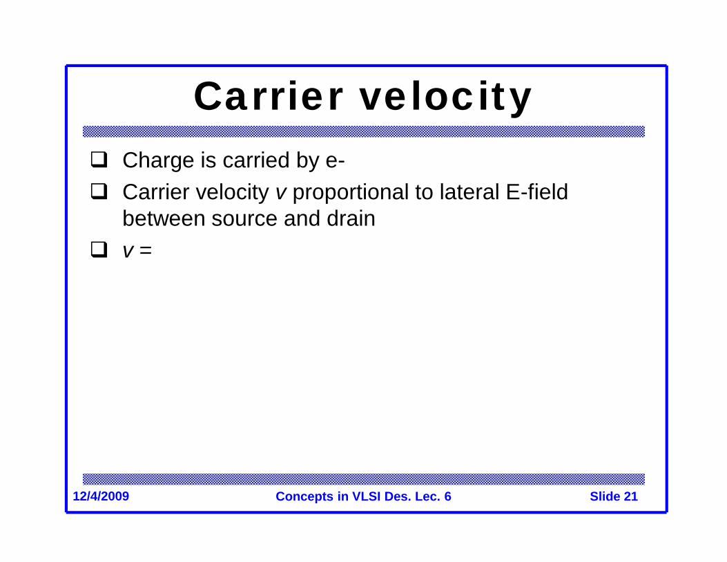
Carrier velocity Charge is carried by e- Carrier velocity v proportional to lateral E-field
between source and drain v =

Concepts in VLSI Des. Lec. 6 Slide 2212/4/2009
Carrier Velocity Charge is carried by e- Carrier velocity v proportional to lateral E-field
between source and drain v = E called mobility E =

Concepts in VLSI Des. Lec. 6 Slide 2312/4/2009
Carrier Velocity Charge is carried by e- Carrier velocity v proportional to lateral E-field
between source and drain v = E called mobility E = Vds/L Time for carrier to cross channel:
– t =

Concepts in VLSI Des. Lec. 6 Slide 2412/4/2009
Carrier Velocity Charge is carried by e- Carrier velocity v proportional to lateral E-field
between source and drain v = E called mobility E = Vds/L Time for carrier to cross channel:
– t = L / v

Concepts in VLSI Des. Lec. 6 Slide 2512/4/2009
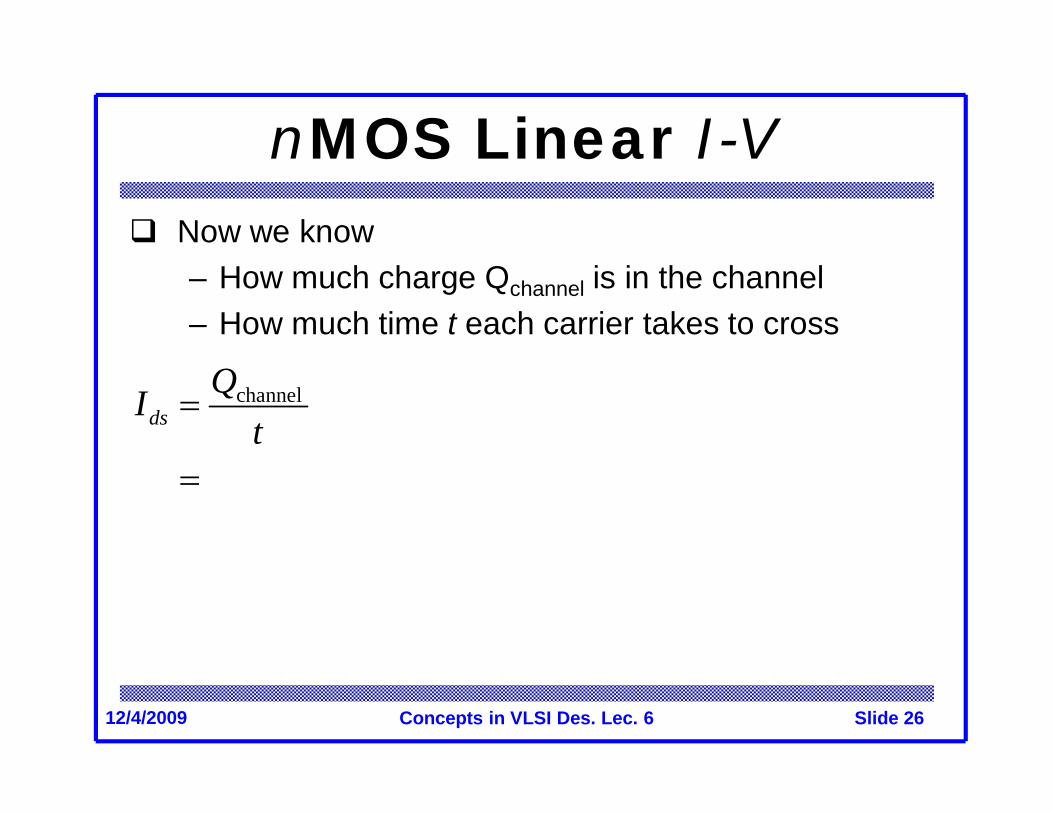
nMOS Linear I-V Now we know
– How much charge Qchannel is in the channel– How much time t each carrier takes to cross
dsI
Concepts in VLSI Des. Lec. 6 Slide 2612/4/2009
nMOS Linear I-V Now we know
– How much charge Qchannel is in the channel– How much time t each carrier takes to cross
channelds
QIt
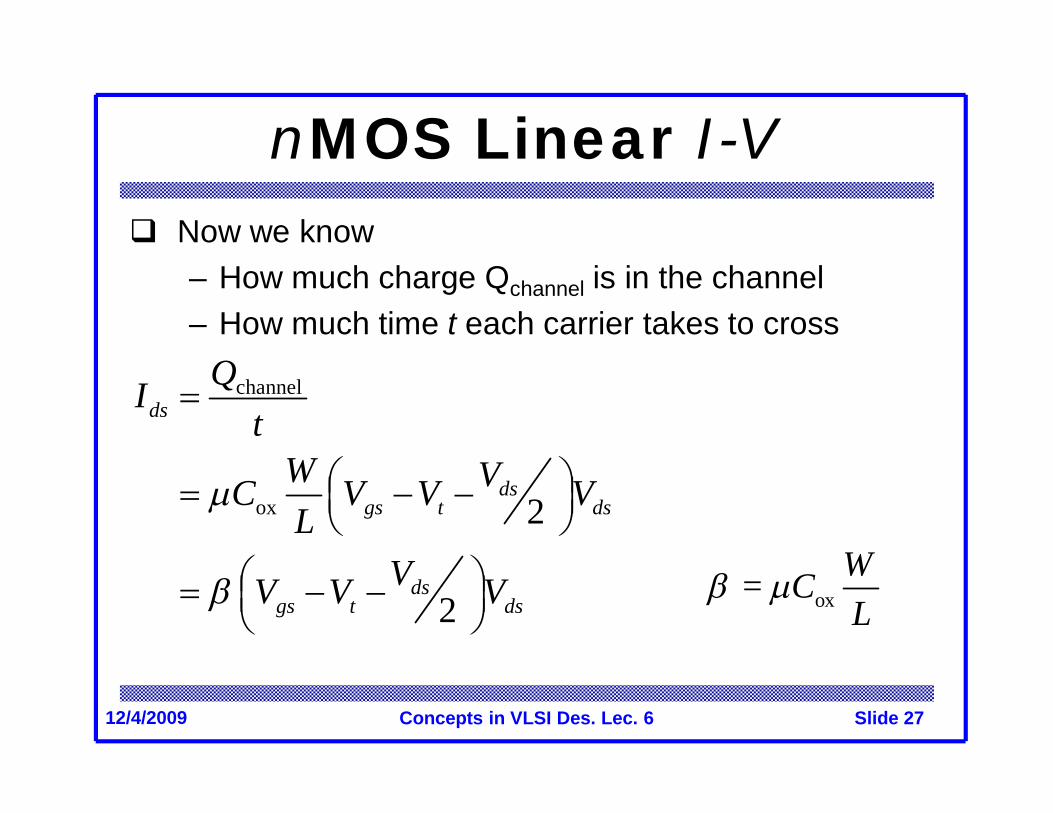
Concepts in VLSI Des. Lec. 6 Slide 2712/4/2009
nMOS Linear I-V Now we know
– How much charge Qchannel is in the channel– How much time t each carrier takes to cross
channel
ox 2
2
ds
dsgs t ds
dsgs t ds
QIt
W VC V V VL
VV V V
ox = WCL
Concepts in VLSI Des. Lec. 6 Slide 2812/4/2009
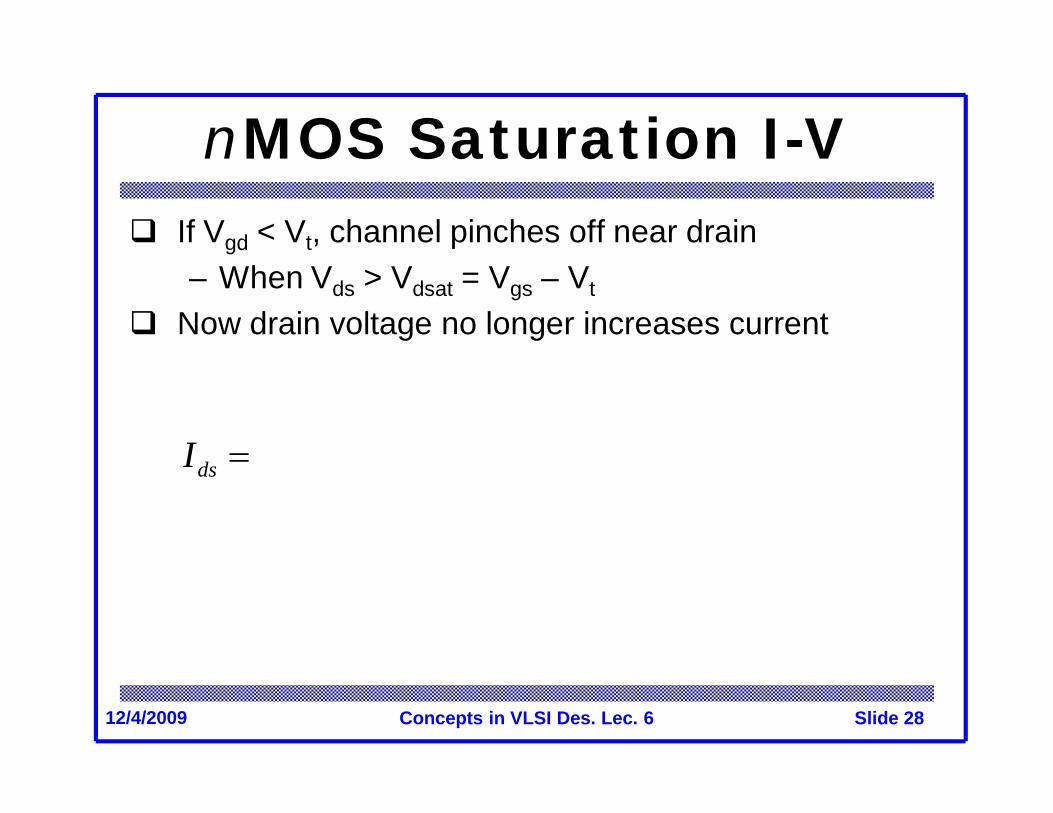
nMOS Saturation I-V If Vgd < Vt, channel pinches off near drain
– When Vds > Vdsat = Vgs – Vt
Now drain voltage no longer increases current
dsI

Concepts in VLSI Des. Lec. 6 Slide 2912/4/2009
nMOS Saturation I-V If Vgd < Vt, channel pinches off near drain
– When Vds > Vdsat = Vgs – Vt
Now drain voltage no longer increases current
2dsat
ds gs t dsatVI V V V

Concepts in VLSI Des. Lec. 6 Slide 3012/4/2009
nMOS Saturation I-V If Vgd < Vt, channel pinches off near drain
– When Vds > Vdsat = Vgs – Vt
Now drain voltage no longer increases current
2
2
2
dsatds gs t dsat
gs t
VI V V V
V V

Concepts in VLSI Des. Lec. 6 Slide 3112/4/2009
nMOS I-V Summary
2
cutoff
linear
saturatio
0
2
2n
gs t
dsds gs t ds ds dsat
gs t ds dsat
V VVI V V V V V
V V V V
Shockley 1st order transistor models

Concepts in VLSI Des. Lec. 6 Slide 3212/4/2009
Example We will be using a 0.6 m process for your project
– From AMI Semiconductor– tox = 100 Å– = 350 cm2/V*s– Vt = 0.7 V
Plot Ids vs. Vds
– Vgs = 0, 1, 2, 3, 4, 5– Use W/L = 4/2
14
28
3.9 8.85 10350 120 /100 10ox
W W WC A VL L L
0 1 2 3 4 50
0.5
1
1.5
2
2.5
Vds
I ds (m
A)
Vgs = 5
Vgs = 4
Vgs = 3
Vgs = 2Vgs = 1

Concepts in VLSI Des. Lec. 6 Slide 3312/4/2009
pMOS I-V All dopings and voltages are inverted for pMOS Mobility p is determined by holes
– Typically 2-3x lower than that of electrons n
– 120 cm2/V*s in AMI 0.6 m process Thus pMOS must be wider to provide same current
– In this class, assume n / p = 2
Concepts in VLSI Des. Lec. 6 Slide 3412/4/2009
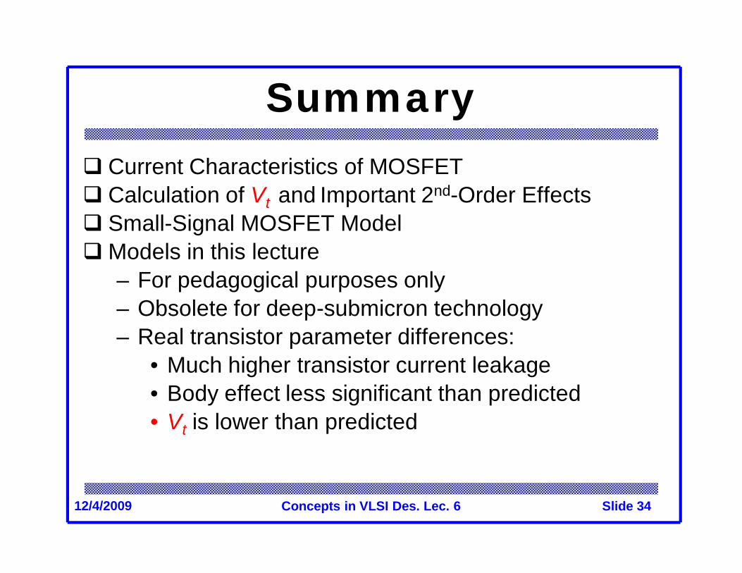
Summary Current Characteristics of MOSFET Calculation of Vt and Important 2nd-Order Effects Small-Signal MOSFET ModelModels in this lecture
– For pedagogical purposes only– Obsolete for deep-submicron technology– Real transistor parameter differences:
• Much higher transistor current leakage• Body effect less significant than predicted• Vt is lower than predicted