Embed Size (px)
Citation preview
Introduction toCMOS VLSI
Design
Lecture 3: CMOS Transistor Theory
David Harris
Harvey Mudd CollegeSpring 2004
3: CMOS Transistor Theory Slide 2CMOS VLSI Design
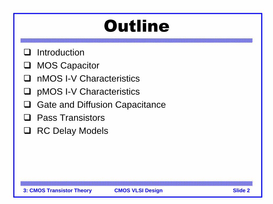
Outlineq Introductionq MOS Capacitorq nMOS I-V Characteristicsq pMOS I-V Characteristicsq Gate and Diffusion Capacitanceq Pass Transistorsq RC Delay Models
3: CMOS Transistor Theory Slide 3CMOS VLSI Design
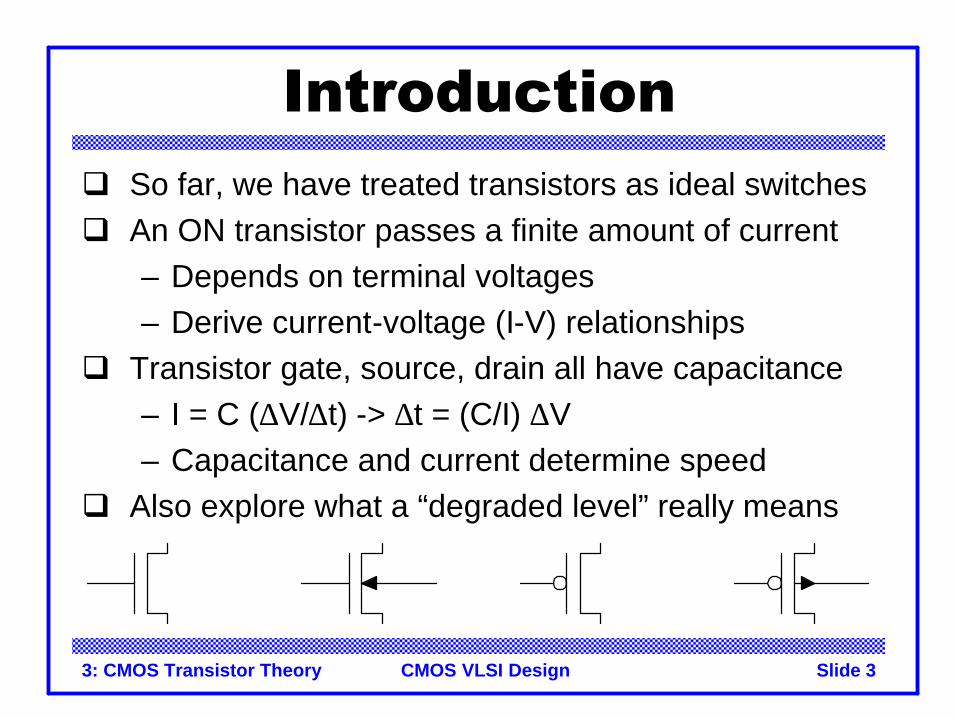
Introductionq So far, we have treated transistors as ideal switchesq An ON transistor passes a finite amount of current
– Depends on terminal voltages– Derive current-voltage (I-V) relationships
q Transistor gate, source, drain all have capacitance– I = C (∆V/∆t) -> ∆t = (C/I) ∆V– Capacitance and current determine speed
q Also explore what a “degraded level” really means
3: CMOS Transistor Theory Slide 4CMOS VLSI Design
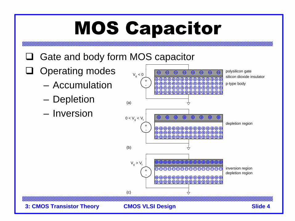
MOS Capacitorq Gate and body form MOS capacitorq Operating modes
– Accumulation– Depletion– Inversion
polysilicon gate
(a)
silicon dioxide insulator
p-type body+-
Vg < 0
(b)
+-
0 < Vg < Vt
depletion region
(c)
+-
Vg > Vt
depletion regioninversion region
3: CMOS Transistor Theory Slide 5CMOS VLSI Design
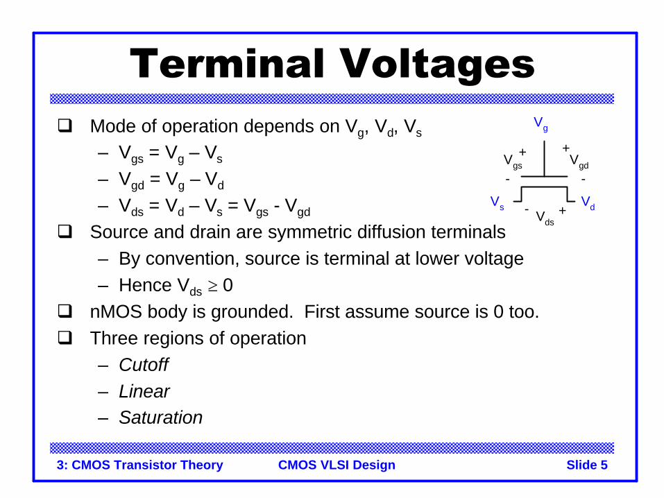
Terminal Voltagesq Mode of operation depends on Vg, Vd, Vs
– Vgs = Vg – Vs
– Vgd = Vg – Vd
– Vds = Vd – Vs = Vgs - Vgd
q Source and drain are symmetric diffusion terminals– By convention, source is terminal at lower voltage– Hence Vds ≥ 0
q nMOS body is grounded. First assume source is 0 too.q Three regions of operation
– Cutoff– Linear– Saturation
Vg
Vs Vd
VgdVgs
Vds+-
+
-
+
-
3: CMOS Transistor Theory Slide 6CMOS VLSI Design
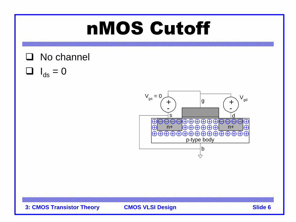
nMOS Cutoffq No channelq Ids = 0
+-
Vgs = 0
n+ n+
+-
Vgd
p-type body
b
g
s d
3: CMOS Transistor Theory Slide 7CMOS VLSI Design
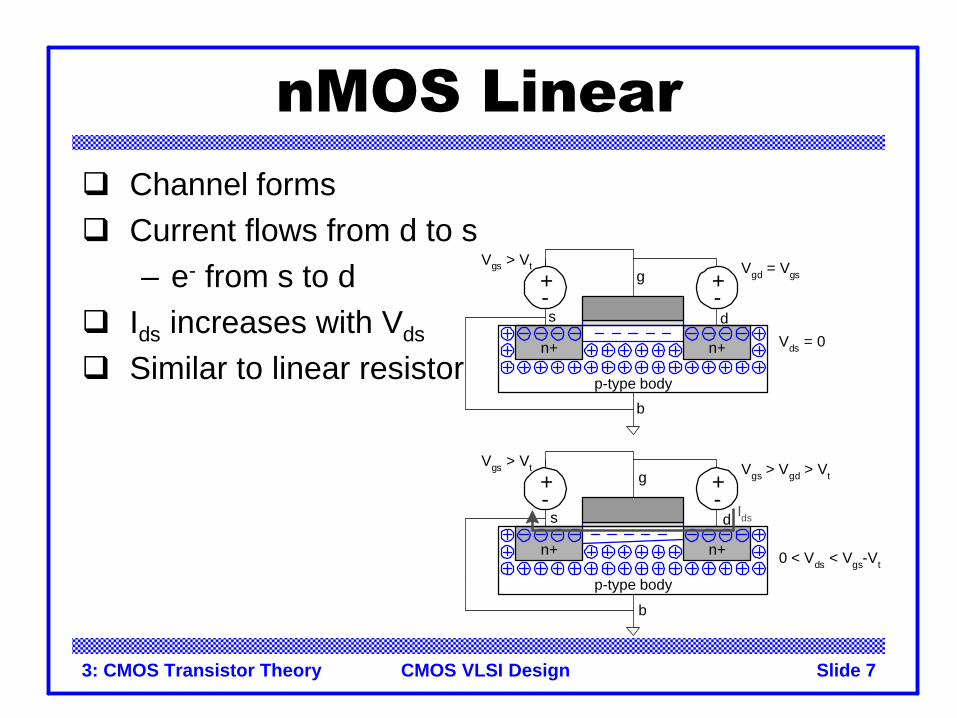
nMOS Linearq Channel formsq Current flows from d to s
– e- from s to dq Ids increases with Vds
q Similar to linear resistor
+-
Vgs > Vt
n+ n+
+-
Vgd = Vgs
+-
Vgs > Vt
n+ n+
+-
Vgs > Vgd > Vt
Vds = 0
0 < Vds < Vgs-Vt
p-type body
p-type body
b
g
s d
b
g
s d Ids
3: CMOS Transistor Theory Slide 8CMOS VLSI Design
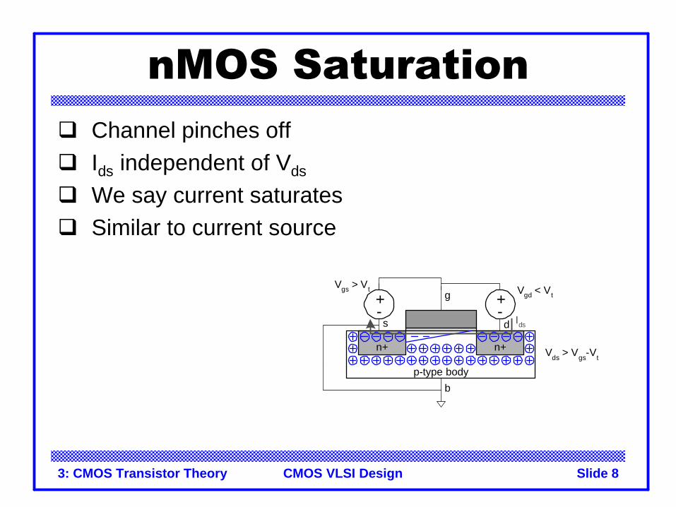
nMOS Saturationq Channel pinches offq Ids independent of Vds
q We say current saturatesq Similar to current source
+-
Vgs > Vt
n+ n+
+-
Vgd < Vt
Vds > Vgs-Vt
p-type body
b
g
s d Ids
3: CMOS Transistor Theory Slide 9CMOS VLSI Design
I-V Characteristicsq In Linear region, Ids depends on
– How much charge is in the channel?– How fast is the charge moving?
3: CMOS Transistor Theory Slide 10CMOS VLSI Design
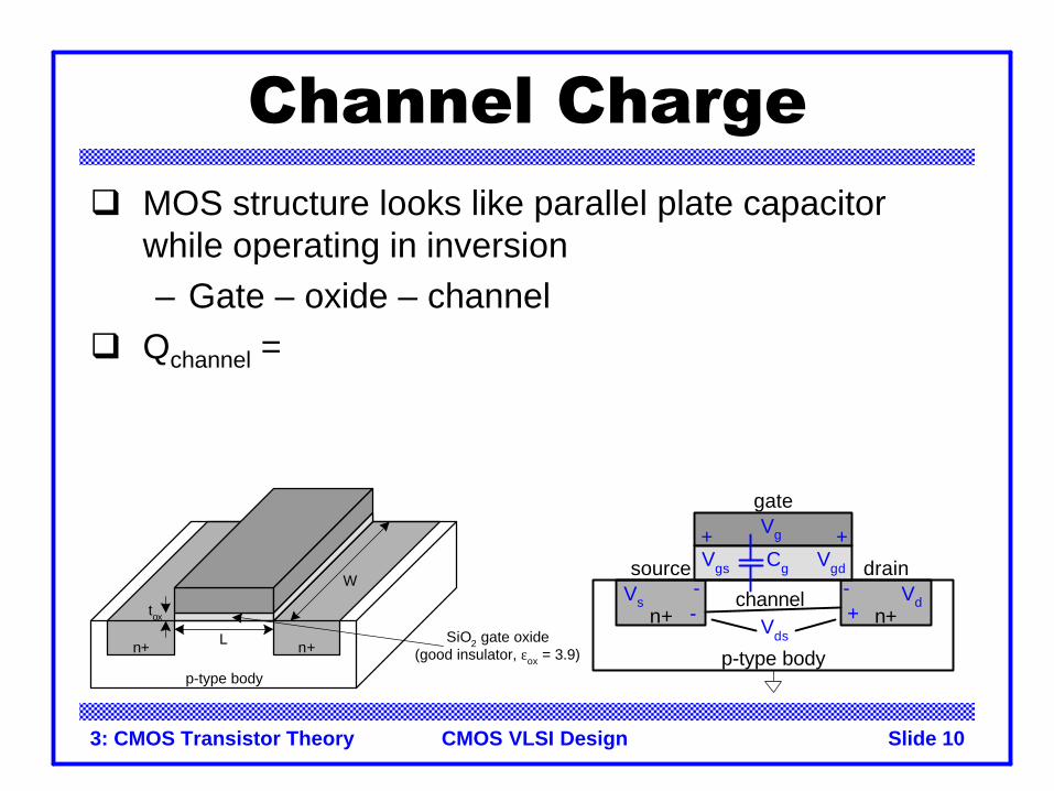
Channel Chargeq MOS structure looks like parallel plate capacitor
while operating in inversion– Gate – oxide – channel
q Qchannel =
n+ n+
p-type body
+
Vgd
gate
+ +
source
-
Vgs
-drain
Vds
channel-
Vg
Vs Vd
Cg
n+ n+
p-type body
W
L
tox
SiO2 gate oxide(good insulator, εox = 3.9)
polysilicongate

3: CMOS Transistor Theory Slide 11CMOS VLSI Design
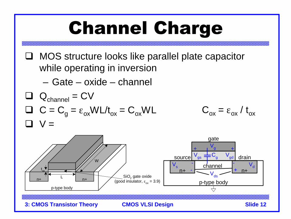
Channel Chargeq MOS structure looks like parallel plate capacitor
while operating in inversion– Gate – oxide – channel
q Qchannel = CVq C =
n+ n+
p-type body
+
Vgd
gate
+ +
source
-
Vgs
-drain
Vds
channel-
Vg
Vs Vd
Cg
n+ n+
p-type body
W
L
tox
SiO2 gate oxide(good insulator, εox = 3.9)
polysilicongate
3: CMOS Transistor Theory Slide 12CMOS VLSI Design
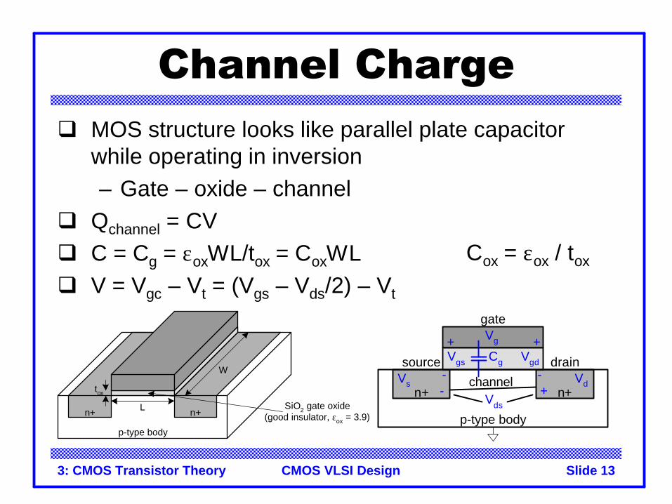
Channel Chargeq MOS structure looks like parallel plate capacitor
while operating in inversion– Gate – oxide – channel
q Qchannel = CVq C = Cg = εoxWL/tox = CoxWLq V =
n+ n+
p-type body
+
Vgd
gate
+ +
source
-
Vgs
-drain
Vds
channel-
Vg
Vs Vd
Cg
n+ n+
p-type body
W
L
tox
SiO2 gate oxide(good insulator, εox = 3.9)
polysilicongate
Cox = εox / tox
3: CMOS Transistor Theory Slide 13CMOS VLSI Design
Channel Chargeq MOS structure looks like parallel plate capacitor
while operating in inversion– Gate – oxide – channel
q Qchannel = CVq C = Cg = εoxWL/tox = CoxWLq V = Vgc – Vt = (Vgs – Vds/2) – Vt
n+ n+
p-type body
+
Vgd
gate
+ +
source
-
Vgs
-drain
Vds
channel-
Vg
Vs Vd
Cg
n+ n+
p-type body
W
L
tox
SiO2 gate oxide(good insulator, εox = 3.9)
polysilicongate
Cox = εox / tox
3: CMOS Transistor Theory Slide 14CMOS VLSI Design
Carrier velocityq Charge is carried by e-q Carrier velocity v proportional to lateral E-field
between source and drainq v =
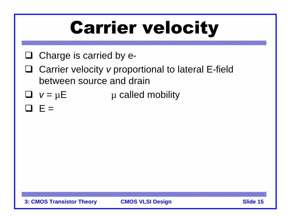
3: CMOS Transistor Theory Slide 15CMOS VLSI Design
Carrier velocityq Charge is carried by e-q Carrier velocity v proportional to lateral E-field
between source and drainq v = µE µ called mobilityq E =
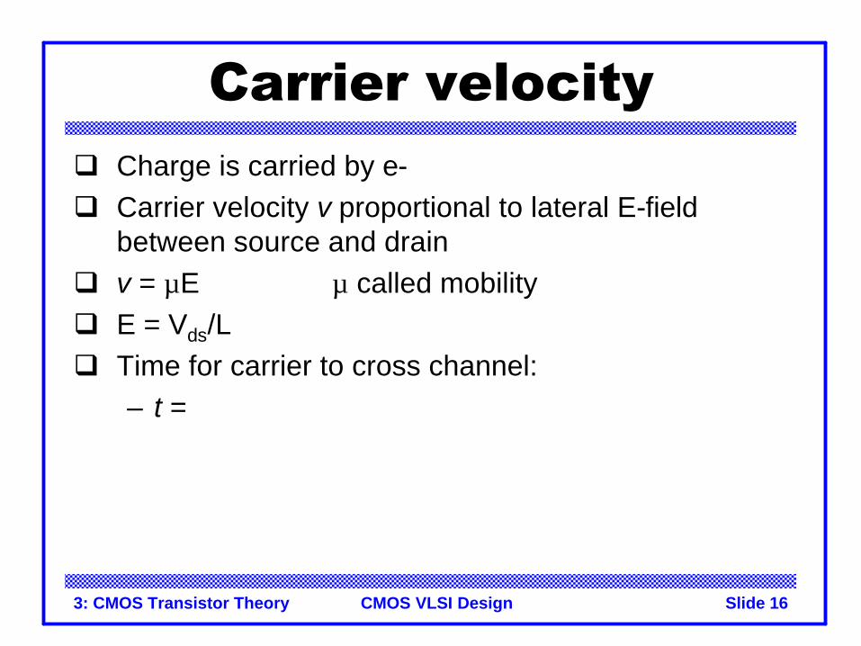
3: CMOS Transistor Theory Slide 16CMOS VLSI Design
Carrier velocityq Charge is carried by e-q Carrier velocity v proportional to lateral E-field
between source and drainq v = µE µ called mobilityq E = Vds/Lq Time for carrier to cross channel:
– t =
3: CMOS Transistor Theory Slide 17CMOS VLSI Design
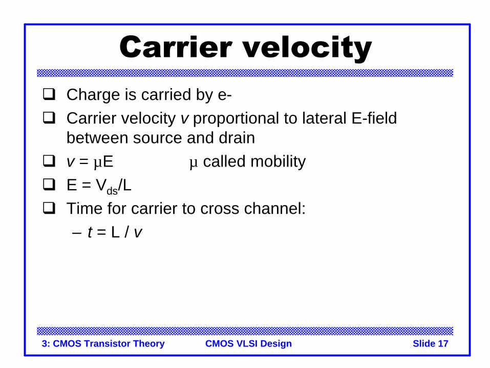
Carrier velocityq Charge is carried by e-q Carrier velocity v proportional to lateral E-field
between source and drainq v = µE µ called mobilityq E = Vds/Lq Time for carrier to cross channel:
– t = L / v
3: CMOS Transistor Theory Slide 18CMOS VLSI Design
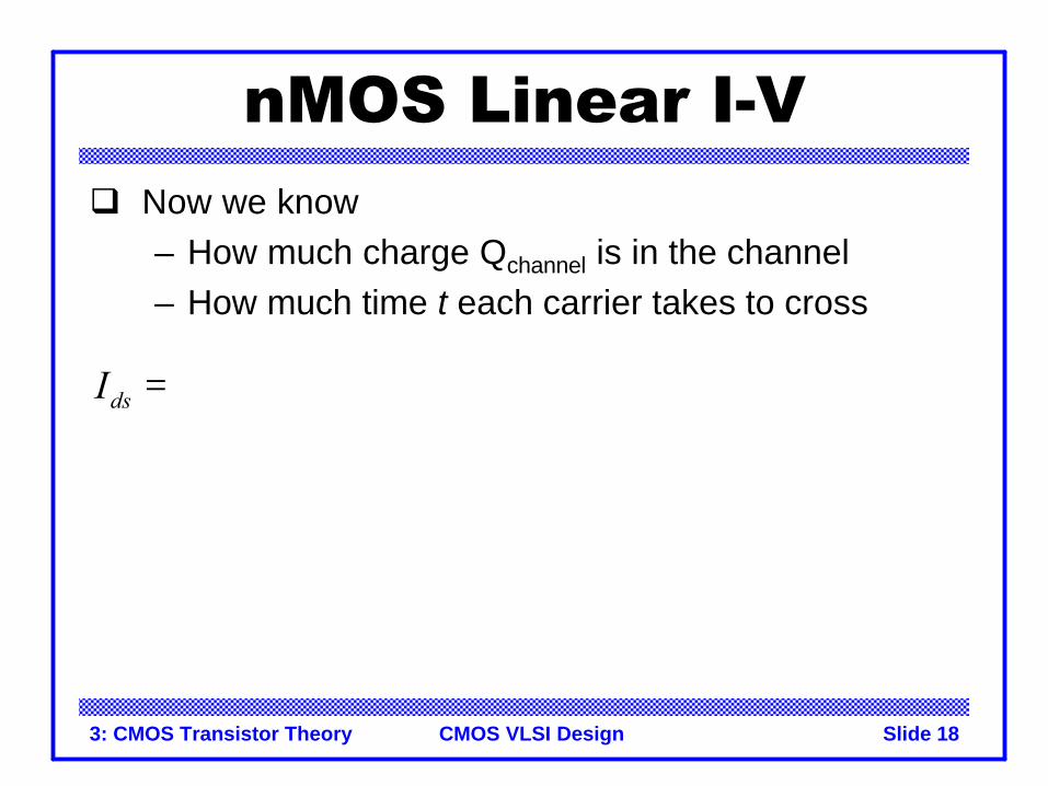
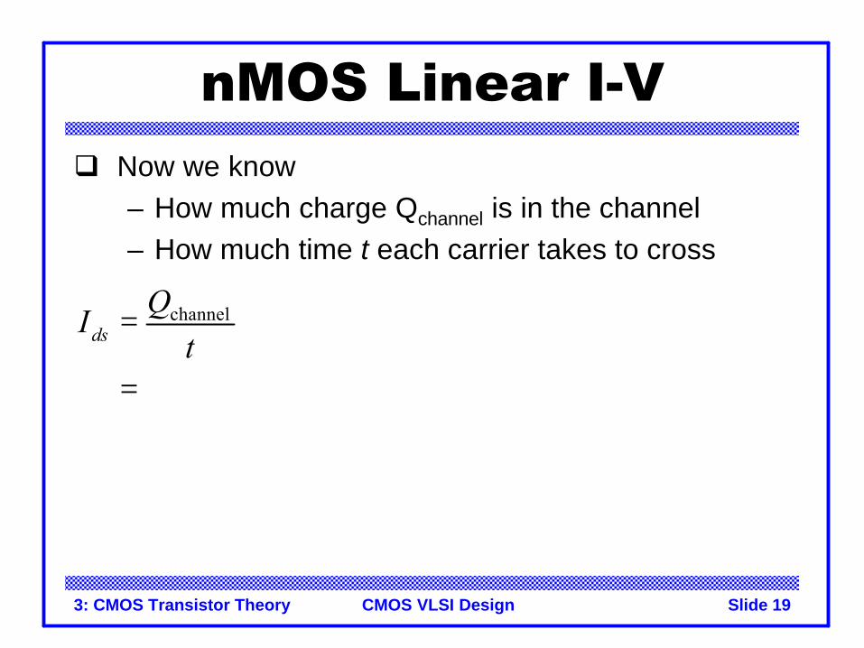
nMOS Linear I-Vq Now we know
– How much charge Qchannel is in the channel– How much time t each carrier takes to cross
dsI =
3: CMOS Transistor Theory Slide 19CMOS VLSI Design
nMOS Linear I-Vq Now we know
– How much charge Qchannel is in the channel– How much time t each carrier takes to cross
channelds
QI
t=
=
3: CMOS Transistor Theory Slide 20CMOS VLSI Design
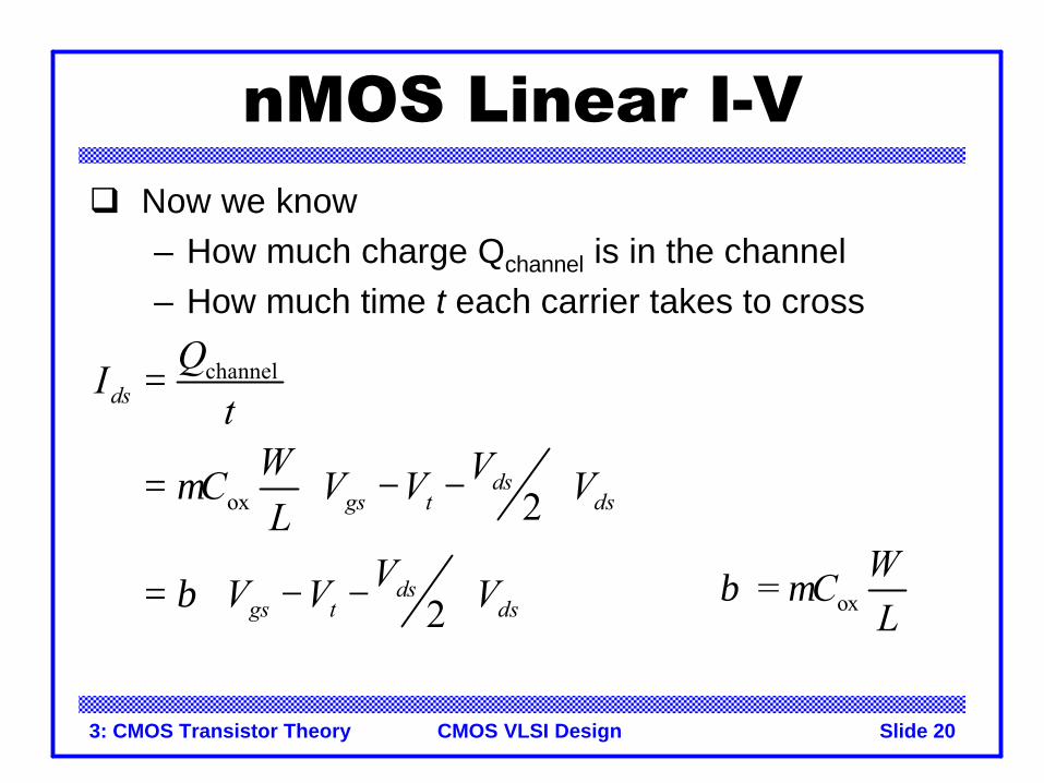
nMOS Linear I-Vq Now we know
– How much charge Qchannel is in the channel– How much time t each carrier takes to cross
channel
ox 2
2
ds
dsgs t ds
dsgs t ds
QI
tW VC V V VL
VV V V
µ
β
=
= − −
= − −
ox = W
CL
β µ
3: CMOS Transistor Theory Slide 21CMOS VLSI Design
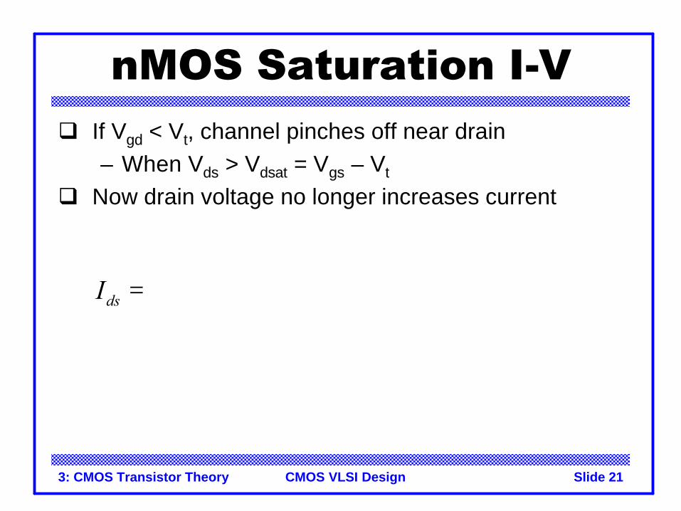
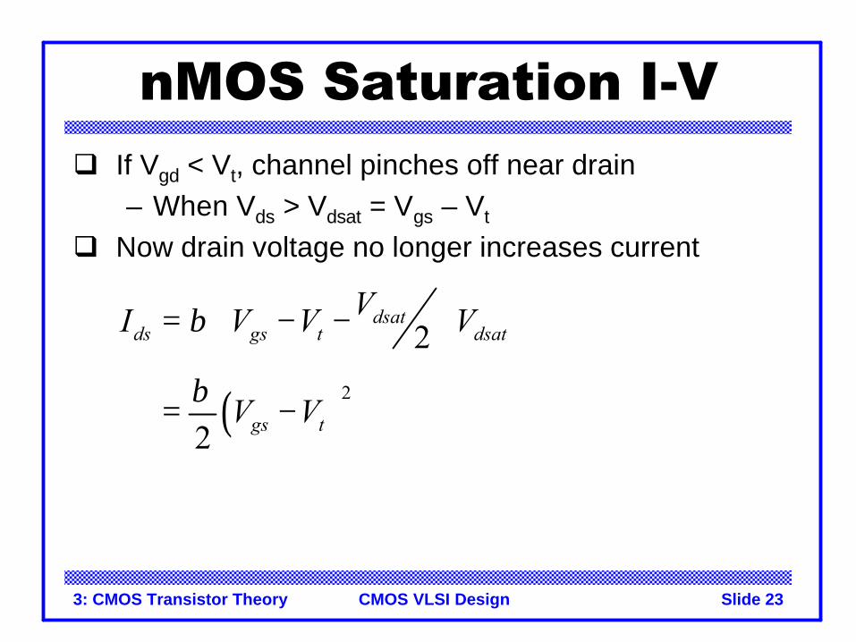
nMOS Saturation I-Vq If Vgd < Vt, channel pinches off near drain
– When Vds > Vdsat = Vgs – Vt
q Now drain voltage no longer increases current
dsI =
3: CMOS Transistor Theory Slide 22CMOS VLSI Design
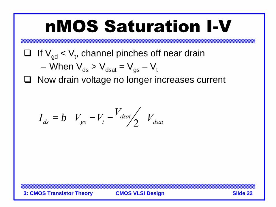
nMOS Saturation I-Vq If Vgd < Vt, channel pinches off near drain
– When Vds > Vdsat = Vgs – Vt
q Now drain voltage no longer increases current
2dsat
ds gs t dsatVI V V Vβ = − −
3: CMOS Transistor Theory Slide 23CMOS VLSI Design
nMOS Saturation I-Vq If Vgd < Vt, channel pinches off near drain
– When Vds > Vdsat = Vgs – Vt
q Now drain voltage no longer increases current
( )2
2
2
dsatds gs t dsat
gs t
VI V V V
V V
β
β
= − −
= −
3: CMOS Transistor Theory Slide 24CMOS VLSI Design
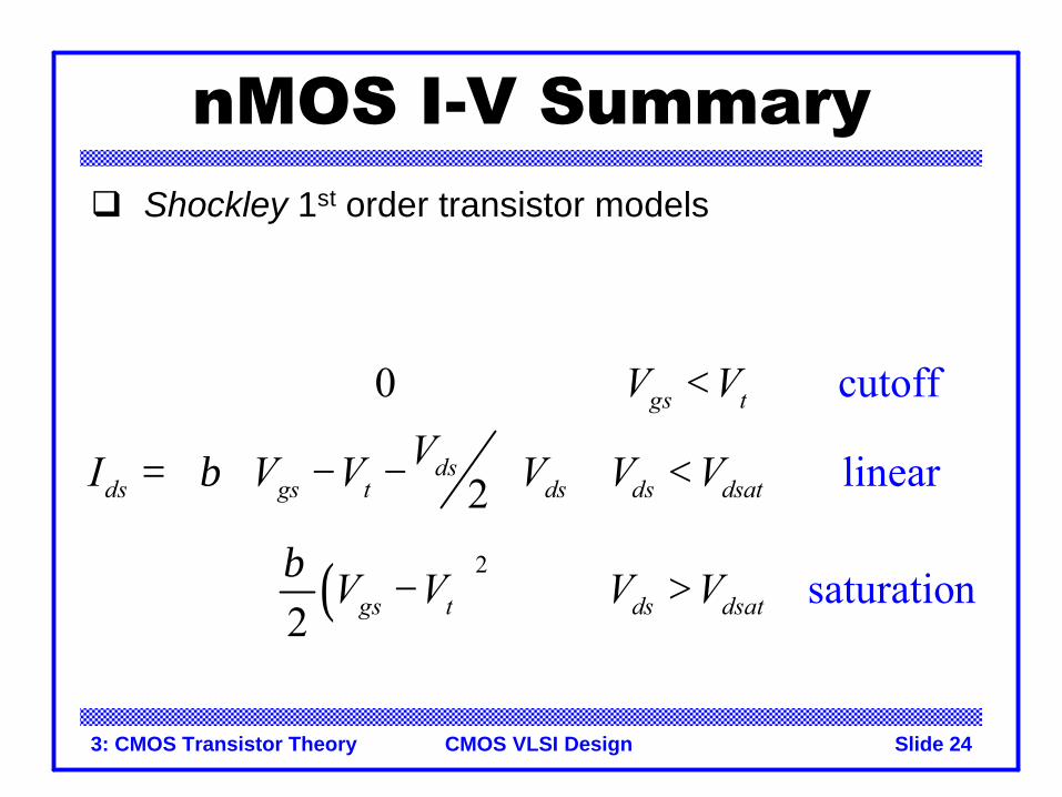
nMOS I-V Summary
( )2
cutoff
linear
saturatio
0
2
2n
gs t
dsds gs t ds ds dsat
gs t ds dsat
V V
VI V V V V V
V V V V
β
β
< = − − <
− >
q Shockley 1st order transistor models
3: CMOS Transistor Theory Slide 25CMOS VLSI Design
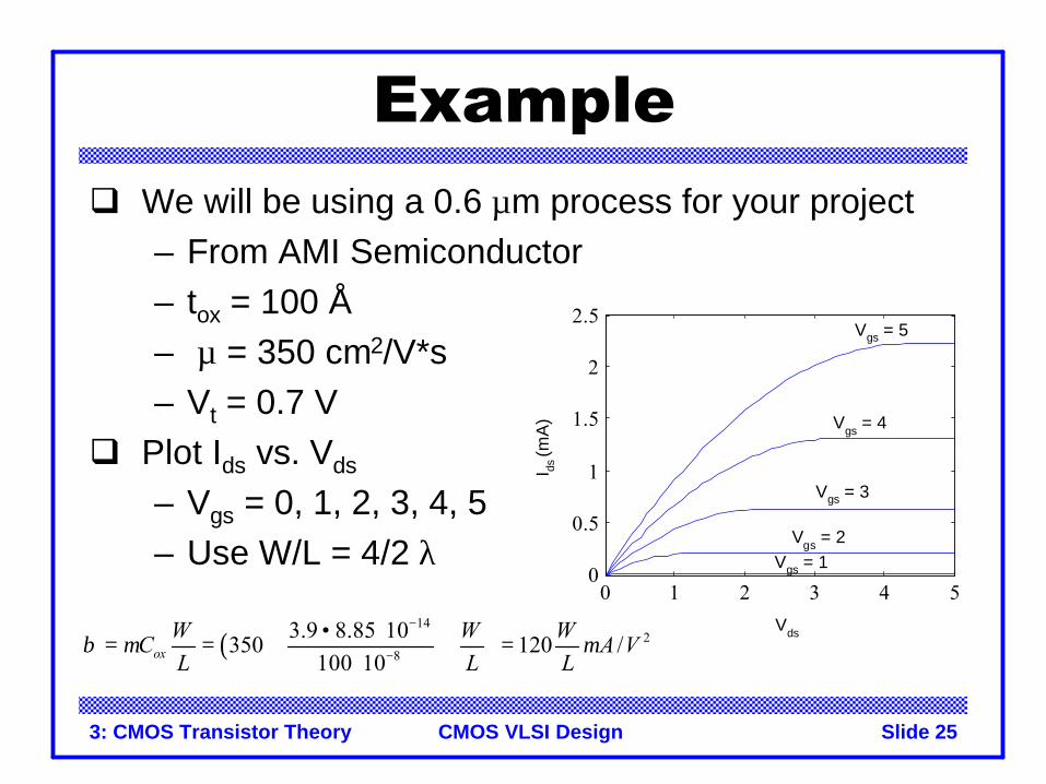
Exampleq We will be using a 0.6 µm process for your project
– From AMI Semiconductor– tox = 100 Å– µ = 350 cm2/V*s– Vt = 0.7 V
q Plot Ids vs. Vds
– Vgs = 0, 1, 2, 3, 4, 5– Use W/L = 4/2 λ
( )14
28
3.9 8.85 10350 120 /
100 10oxW W W
C A VL L L
β µ µ−
−
• ⋅ = = = ⋅
0 1 2 3 4 50
0.5
1
1.5
2
2.5
Vds
I ds (m
A)
Vgs = 5
Vgs = 4
Vgs = 3
Vgs = 2Vgs = 1
3: CMOS Transistor Theory Slide 26CMOS VLSI Design
pMOS I-Vq All dopings and voltages are inverted for pMOSq Mobility µp is determined by holes
– Typically 2-3x lower than that of electrons µn
– 120 cm2/V*s in AMI 0.6 µm processq Thus pMOS must be wider to provide same current
– In this class, assume µn / µp = 2
– *** plot I-V here
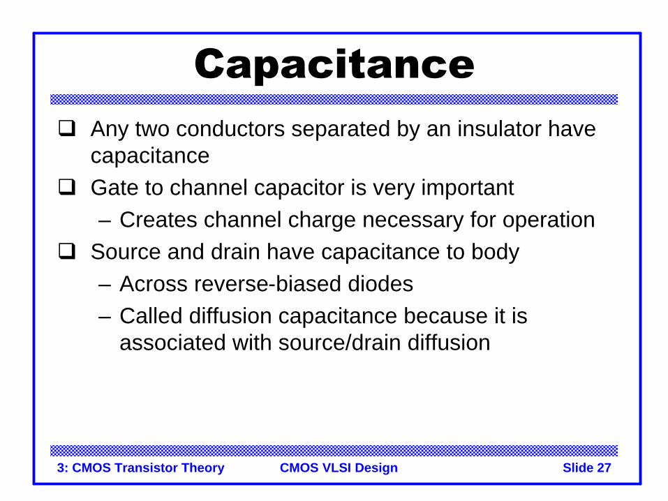
3: CMOS Transistor Theory Slide 27CMOS VLSI Design
Capacitanceq Any two conductors separated by an insulator have
capacitanceq Gate to channel capacitor is very important
– Creates channel charge necessary for operationq Source and drain have capacitance to body
– Across reverse-biased diodes– Called diffusion capacitance because it is
associated with source/drain diffusion
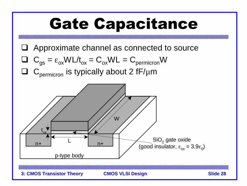
3: CMOS Transistor Theory Slide 28CMOS VLSI Design
Gate Capacitanceq Approximate channel as connected to sourceq Cgs = εoxWL/tox = CoxWL = CpermicronWq Cpermicron is typically about 2 fF/µm
n+ n+
p-type body
W
L
tox
SiO2 gate oxide(good insulator, εox = 3.9ε0)
polysilicongate
3: CMOS Transistor Theory Slide 29CMOS VLSI Design
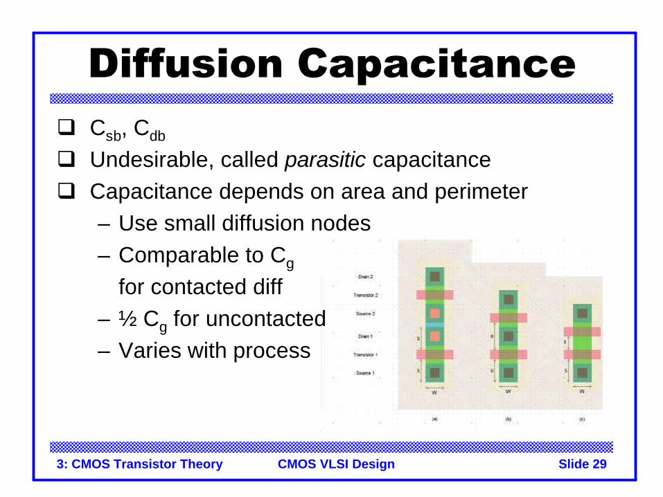
Diffusion Capacitanceq Csb, Cdb
q Undesirable, called parasitic capacitanceq Capacitance depends on area and perimeter
– Use small diffusion nodes– Comparable to Cg
for contacted diff– ½ Cg for uncontacted– Varies with process
3: CMOS Transistor Theory Slide 30CMOS VLSI Design
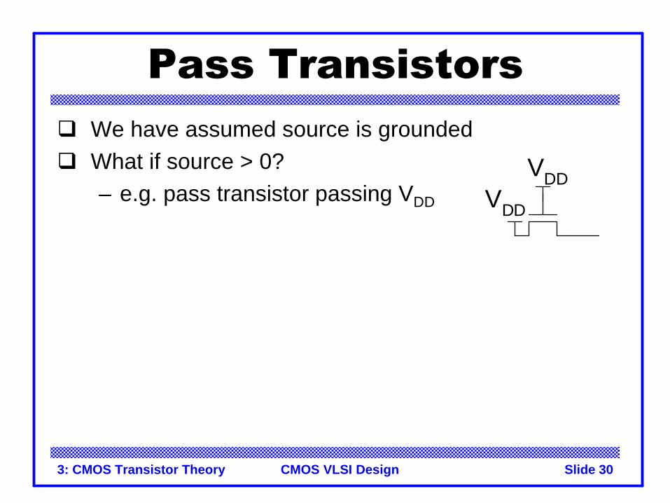
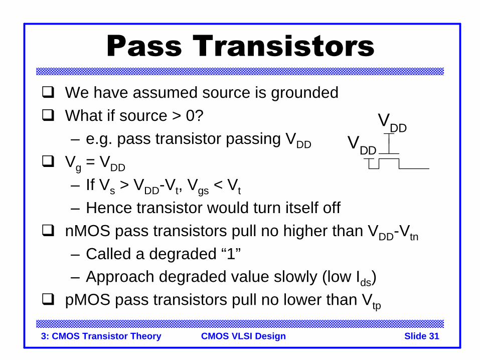
Pass Transistorsq We have assumed source is groundedq What if source > 0?
– e.g. pass transistor passing VDD
VDDVDD
3: CMOS Transistor Theory Slide 31CMOS VLSI Design
Pass Transistorsq We have assumed source is groundedq What if source > 0?
– e.g. pass transistor passing VDD
q Vg = VDD
– If Vs > VDD-Vt, Vgs < Vt
– Hence transistor would turn itself offq nMOS pass transistors pull no higher than VDD-Vtn
– Called a degraded “1”– Approach degraded value slowly (low Ids)
q pMOS pass transistors pull no lower than Vtp
VDDVDD
3: CMOS Transistor Theory Slide 32CMOS VLSI Design
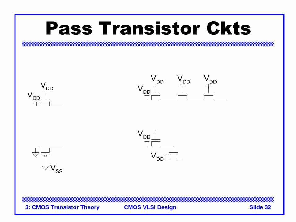
Pass Transistor Ckts
VDDVDD
VSS
VDD
VDD
VDD VDD VDD
VDD
3: CMOS Transistor Theory Slide 33CMOS VLSI Design
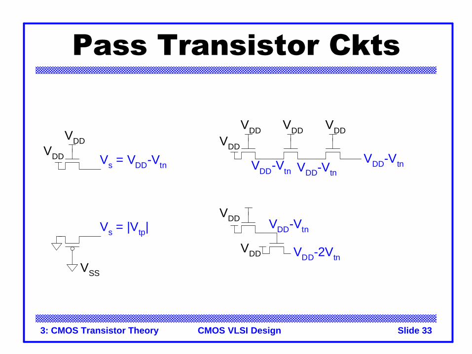
Pass Transistor Ckts
VDDVDD Vs = VDD-Vtn
VSS
Vs = |Vtp|
VDD
VDD-Vtn VDD-Vtn
VDD-Vtn
VDD
VDD VDD VDD
VDD
VDD-Vtn
VDD-2Vtn
3: CMOS Transistor Theory Slide 34CMOS VLSI Design
Effective Resistanceq Shockley models have limited value
– Not accurate enough for modern transistors– Too complicated for much hand analysis
q Simplification: treat transistor as resistor– Replace Ids(Vds, Vgs) with effective resistance R
• Ids = Vds/R– R averaged across switching of digital gate
q Too inaccurate to predict current at any given time– But good enough to predict RC delay
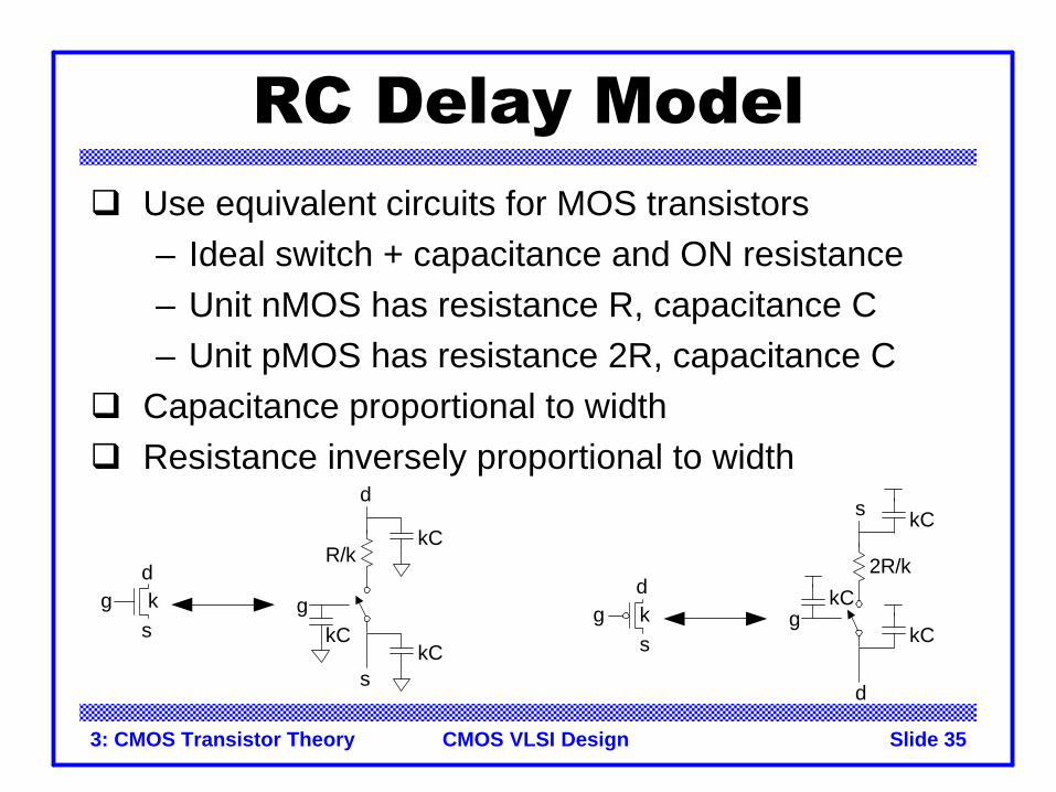
3: CMOS Transistor Theory Slide 35CMOS VLSI Design
RC Delay Modelq Use equivalent circuits for MOS transistors
– Ideal switch + capacitance and ON resistance– Unit nMOS has resistance R, capacitance C– Unit pMOS has resistance 2R, capacitance C
q Capacitance proportional to widthq Resistance inversely proportional to width
kgs
d
g
s
d
kCkC
kCR/k
kgs
d
g
s
d
kC
kC
kC
2R/k
3: CMOS Transistor Theory Slide 36CMOS VLSI Design
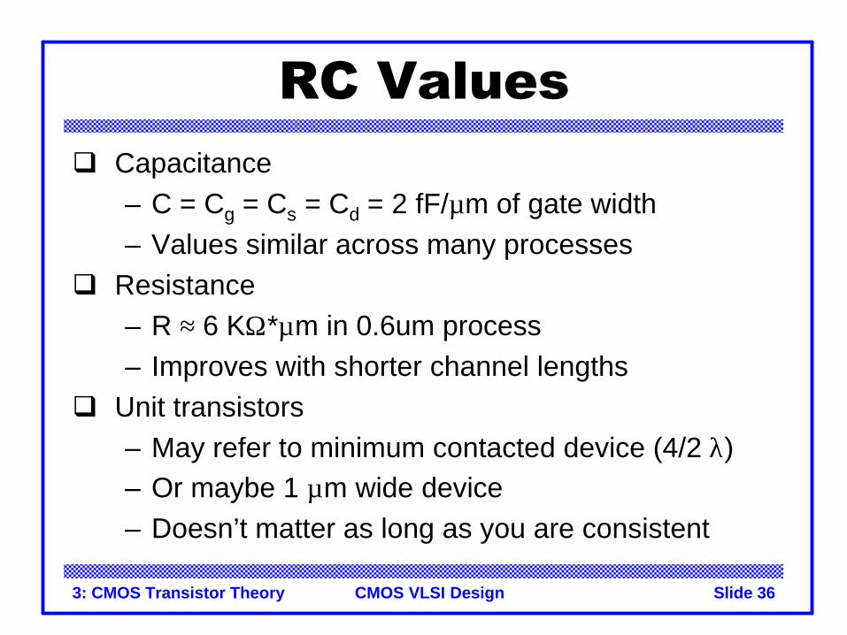
RC Valuesq Capacitance
– C = Cg = Cs = Cd = 2 fF/µm of gate width– Values similar across many processes
q Resistance– R ≈ 6 KΩ*µm in 0.6um process– Improves with shorter channel lengths
q Unit transistors– May refer to minimum contacted device (4/2 λ)– Or maybe 1 µm wide device– Doesn’t matter as long as you are consistent
3: CMOS Transistor Theory Slide 37CMOS VLSI Design
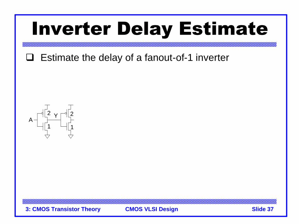
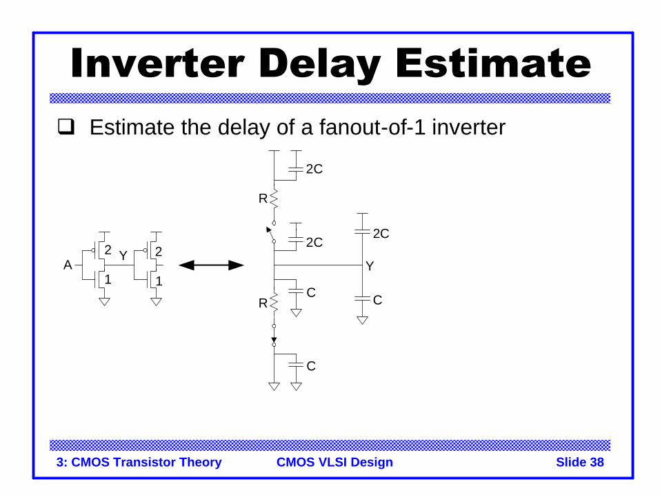
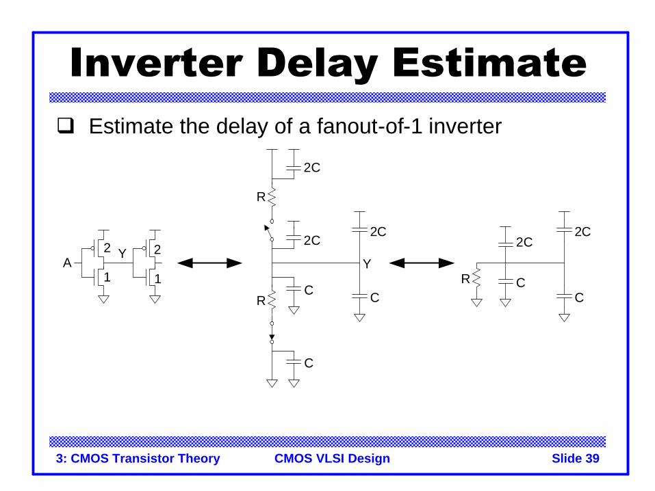
Inverter Delay Estimateq Estimate the delay of a fanout-of-1 inverter
2
1A
Y 2
1
3: CMOS Transistor Theory Slide 38CMOS VLSI Design
Inverter Delay Estimateq Estimate the delay of a fanout-of-1 inverter
C
CR
2C
2C
R
2
1A
Y
C
2C
Y2
1
3: CMOS Transistor Theory Slide 39CMOS VLSI Design
Inverter Delay Estimateq Estimate the delay of a fanout-of-1 inverter
C
CR
2C
2C
R
2
1A
Y
C
2C
C
2C
C
2C
RY
2
1
3: CMOS Transistor Theory Slide 40CMOS VLSI Design
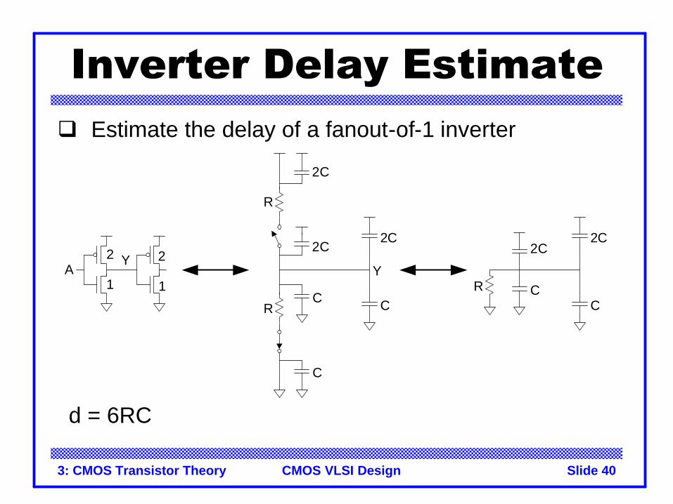
Inverter Delay Estimateq Estimate the delay of a fanout-of-1 inverter
C
CR
2C
2C
R
2
1A
Y
C
2C
C
2C
C
2C
RY
2
1
d = 6RC