Embed Size (px)
Citation preview

CONVEX Processor Diagnostics Manual (Cl, C120)
Document No. 760-000950-200
Version 1.0 April 1988
CONVEX Computer Corporation Richardson, Texas USA
CONVEX Processor Diagnostics Manual (01, 0120}
Order No. DHWG071 Version 1.0
© 1988 CONVEX Computer Corporation All rights reserved.
This document is copyrighted. All rights are reserved. This document may not, in whole or part, be copied, duplicated, reproduced, translated, electronically stored or reduced to machine readable form without prior written consent from CONVEX Computer Corporation (CONVEX).
Although the material contained herein has been carefully reviewed, CONVE.,"I{ does not warrant it to be Cree of errors or omissions. CONVEX reserves the right to make corrections, updates, revisions, or changes t.o the information contained herein. CONVEX does not warrant the material described herein to be free of patent infringement.
UNLESS PROVIDED OTHERWISE IN WRITING WITH CONVEX COl\IIPUTER CORPORATION (CONVEX), THE EQUIPMENT DESCRIBED HEREIN IS PROVIDED "AS IS" WITHOUT WARRANTY OF ANY KIND, EITHER EXPRESSED OR IMPLIED, INCLUDING, BUT NOT LIMITED TO, THE IMPLIED WARRANTIES OF MERCHANTABil.ITY AND FITNESS FOR A PARTICULAR PURPOSE. SOl\IIE STATES DO NOT ALLOW THE EXCLUSION OF IMPLIED WARRANTIES. THE ABOVE EXCLUSION MAY NOT BE APPLICABLE TO ALL PURCHASERS BECAUSE WARRANTY RIGHTS CAN VARY FROM STATE TO STATE. IN NO EVENT Wil.L CONVEX BE LIABLE TO ANYONE FOR SPECIAL, COLLATERAL, INCIDENTAL, OR CONSEQUENTIAL DAMAGES, INCLUDING ANY LOST PROFITS OR LOST SAVINGS, ARISING OUT OF THE USE OR INABILITY TO USE THIS EQUIPMENT. CONVEX Wil.L NOT BE LIABLE EVEN IF IT HAS BEEN NOTIFIED OF THE POSSIBILITY OF SUCH DAMAGE BY THE PURCHASER OR ANY THIRD PARTY.
CONVEX and the CONVEX logo ("C") are registered tra.dema.rks of CONVEX Computer Corporation Cl, Cl20, C130, C210, C220, contact, and EGOS are trademarks of CONVEX Computer Corporation
UNIX is a registered trademark of AT&T Bell Laboratories
Printed in the United States of America
1.0
Revision Sheet CONVEX Processor Diagnostics Manual
{Cl, C120}
760-000950-200 Apr 88 First release, Version 1.0. This manual contains all processor-dependent diagnostics for the CONVEX Cl and 0120 computers.
THIS PAGE INTENTIONALLY LEFT BLANK
Table of Contents
1 Diagnostics 1.1 Diagnostic Test Overview ................................................................................................... 1-1
1.1.1 Reference Structure .................................................................................................... 1-2 1.2 Functional Tests ................................................................................................................. 1-2 1.3 Utilities .............................................................................................................................. 1-2
2 Dshell and Scan Overview 2.1 Overvie\v ............................................................................................................................ 2-1 2.2 Diagnostic Shell ( dshell) Overview ..................................................................................... 2-1 2.3 Syntax Help for dshell Commands ..................................................................................... 2-:3 2.4 Scan Overview .................................................................................................................... 2-:3 2.5 Scan Commands ................................................................................................................. 2-4
spulOOO SPU Self Test Introduction .................................................................................................................. spul000-1 Program Invocation ...................................................................................................... spul000-1
User Interface .......................................................................................................... spul000-1 Class Descriptions ......................................................................................................... spul000-2 Subtest Descriptions ...................................................................................................... spul000-2
CPUl Test .............................................................................................................. spul000-:3 ROM Test ............................................................................................................... spul000-4 CPU2 Test .............................................................................................................. spul000-4 RAMl Test ............................................................................................................. spul000-4 CPU3 Test .............................................................................................................. spul000-5 Timer Test .............................................................................................................. spul000-5 Console Test ........................................................................................................... spul000-6 Remote Test ........................................................................................................... spul000-6 RAM2 Test ............................................................................................................. spul000-6 Map Test ................................................................................................................ spul000-6 RAM3 Test ............................................................................................................. spul000-7 Boot Device Test ..................................................................................................... spul000-7
Error Messages ............................................................................................................. spul000-8 SPU Self Test Error Codes ............................................................................ spul000-8
Boot Devices Error Codes ...................................................................................... spu 1000-11
spu2000 SPU Peripher'al Test Introduction .................................................................................................................. spu2000- l Test Program Invocation .............................................................................................. spu2000- l
User Interface .......................................................................................................... spu2000-l UNIX Root RESTORE Function ................................................................... spu2000-2 Disk/Tape Format/Test Function .................................................................. spu2000-:3 Subtest Enable ............................................................................................... spu2000-5 SPU Hardware Utility .................................................................................... spu2000-5
Class Descriptions ......................................................................................................... spu2000-i) Subtest Descriptions ...................................................................................................... spu2000-5
Maintenance Track Subtest ..................................................................................... spu2000-6 Format Subtest ....................................................................................................... spu2000-8 Write Subtest .......................................................................................................... spu2000-8 Read Subt.est ............................................................................................................ ,.;pu2000-8 Bad Block Fix Su ht.est ............................................................................................. spu2000-8
v

Random Read Subtest ....................................................................... · · · · · · · · · · · · · · · · · · · · · · spu2000-8 Seek Subtest ........................................................................................ · · ··· · · ··· ··· · ·· · ·· spu2000-9 Other Subtest Options ............................................................................... ··. ·· ·· ··· · ·· spu2000-9
Execution Time ......................................................................................................... · · · spu2000-9 Error Messages ........................................................................................................... · · spu2000-9
Error Descriptions ................................................................................................. spu2000-10
spu4000 SPU Kernel Test Introduction .................................................................................................................. spu4000- l Test Program Invocation .............................................................................................. spu4000-1 Class Descriptions ......................................................................................................... spu4000-:3 Subtest Descriptions ...................................................................................................... spu4000-4
SPU Control Register Test ...................................................................................... spu4000-i DBUS Interface Test ............................................................................................... spu4000-i Board ID Test ......................................................................................................... spu4000-i Scan Ring Integrity Test ......................................................................................... spu4000-i Hard-Error Recognition Test ................................................................................... spu4000-8 Power and Clock Margin Test ................................................................................. spu4000-8 PBUS Integrity ............................................................................................... , ....... spu4000-8 PBUS Interrupt Test ............................................................................................... spu4000-9
Failure Messages ......................................................................................................... spu4000-10
spu4100 SPU Cartridge Tape and File System Test Introduction .................................................................................................................. spu4100-l Test Invocation ............................................................................................................. spu4100-l Class Descriptions ......................................................................................................... spu4100-:3
Pattern Tests .......................................................................................................... spu4100-:3 Seek Tests ............................................................................................................... spu4100-:3
Subtest Descriptions ...................................................................................................... spu4100--t Arbitrary Pattern Write Test .................................................................................. spu4100-4 Arbitrary Pattern Read Test ................................................................................... spu4100--t Write Seek Test Pattern Test .................................................................................. spu4100-4 Seek Test ................................................................................................................ spu4100-4
Failure Messages ........................................................................................................... spu4100-5 Error Nlessages ............................................................................................................. spu4100-5
mem4000 Main Memory Test Introduction ............................................................................................................... mem-1000-1 Test Invocation ........................................................................................................... mem-1000-1 Class Descriptions ....................................................................................................... mem4000--t
Class 1 Sub tests .................................................................................................... mem4000-4 Class 2 Subtests .................................................................................................... mem4000-4 Class 3 Sub tests .................................................................................................... mem4000-4 Class 4 Sub tests .................................................................................................... 1ne1114000-5 Class 5 Sub tests .................................................................................................... mem4000-5 Class 6 Sub tests .................................................................................................... meni,1000-5 Class 7 Subtests .................................................................................................... mem-LOOO-;) Class 8 Subtests .................................................................................................... mem--1000-5 Class 9 Sub tests .................................................................................................... n1e1114000-6
Subtest Descriptions ................................................................................................... mem--1000-G Data-Output Shorts Test ...................................................................................... mem-IOOO-~ .\ddress Uniqueness Test ....................................................................................... menl"I000-8 Cross-Talk Test .................................................................................................... mem 1000-~
vi

~ I
Refresh Test ......................................................................................................... mem4000-8 Address Shorts Test .............................................................................................. 1nen14000-8 Byte Merge Test ................................................................................................... mem4000-9 Test-and-Set Test ................................................................................................. 1nein4000-9 Unaligned Block Read Test ................................................................................... mem4000-9 Unaligned Block Write Test .................................................................................. mem4000-!l Soft-Error Log Interface Test ................................................................................ mem4000-9 Check-Bit Forced Read/Write Test ..................................................................... mem4000-10 Check-Bit Generation Test .................................................................................. mem4000-10 Check-Bit Output Shorts Test ............................................................................. mem4000-10 Check-Bit Generation Test .................................................................................. mem4000- l O Single-Bit Error Detection/Correction Test ......................................................... mem4000-10 Double-Bit Error Detection Test .......................................................................... mem4000-ll l'vlemory Scrub Test ............................................................................................. mem4000-11 Address Error Test .............................................................................................. mem4000-11 PBUS Parity Error Test ...................................................................................... mem4000-11 Memory Sizing Test ............................................................................................ mem4000- l:.l Hard/Soft Interrupt Test .................................................................................... mem4000-1:.l Address Uniqueness with EDC ............................................................................. mem4000-1:.l Cross-Talk Test with EDC .................................................................................. mem4000-1:.l Refresh Test with EDC ....................................................................................... mem4000-1:.l Vectorized Address Uniqueness Test .................................................................... mem4000-1:.l Vectorized Cross-Talk Test ................................................................................. mem4000-1:3 Vectorized Refresh Test ....................................................................................... mem4000-1:3 Address Uniqueness with EDC ............................................................................. mem4000-1:3 Vectorized Cross-Talk Test with EDC ................................................................. mem4000-1:3 Vectorized Refresh Test with EDC ...................................................................... mem4000-1:3 Vectorized Address-Address Complement ............................................................ mem4000-1:3 Main Memory Interleave Test ............................................................................. mem4000-14
Error Messages .......................................................................................................... mem4000-15
cpu4000 CPU Instruction Set Test Introduction ................................................................................................................. cpu4000-1 Test Invocation ............................................................................................................. cpu4000-l Class Descriptions ......................................................................................................... cpu4000-4
Instruction Set Tests ............................................................................................... cpu4000-4 Boundary Conditions Tests ..................................................................................... cpu-1000-·l Exception Tests ...................................................................................................... qrn-1000-.) Cache Feature Tests ............................................................................................... cpu4000-.) IEEE Floating Point Tests ...................................................................................... cpu4000-.)
Subtest Descriptions ..................................................................................................... cpu-1000-.) Class 9-16 subtests ................................................................................................ cpu4000-1:.l
Subtests 100-820 .......................................................................................... cpu4000-1:.l Class 20 sub tests ................................................................................................... cpu4000-1 :.l
Subtest 900: adbnd_ld.s ............................................................................... cpu4000- l:.l Subtest 901: pgbnd_ld.s ............................................................................... cpu4000-1:.l Subtest 902: nrpgbnd_ld.s ............................................................................ rpu·I000-1:.! Subtest 905: adbnd_st.s ................................................................................ cpu4000-l:.l Subtest 906: pgbnd_st.s ................................................................................ cpu4000-l:.l Subtest 907: nrpgbncl_st.s ............................................................................ cpu4000- l ;3 Subtest 908: pgbnd_inld.:; ............................................................................. cptt·I000-1:) Subtest 909: nrpgbnd_inld.s ......................................................................... cpul000-1:\ Subtest. !llO: pgbncl_t'x.s ............................................................................... cpu-!000-1 ;)
vii

Subtest 911: expgbnd.s ................................................................................. cpu4000-13 Subtest 912: nrpgbnd_ex.s ............................................................................ cpu4000-13 Subtest 913: nrexpgbnd.s ............................................................................. cpu4000-14 Subtest 917: nrpgbnd_br.s ............................................................................ cpu4000-14 Subtest 920: stepgbnd.s ............................................................................... cpu4000-14 Subtest 922: nrstepgbnd.s ............................................................................ cpu4000-14 Subtest 923: stei.s ........................................................................................ cpu4000-14 Subtest 924: asuvcuq.s ................................................................................. cpu4000-14 Subtest 925: vlzero.s .................................................................................... cpu4000-14 Subtest 926: vsvar.s ..................................................................................... cpu4000-14 Subtest 927: vex.s ........................................................................................ cpu4000-14 Subtest 928: vbpg.s ...................................................................................... cpu4000-15 Subtest 929: vhpg.s ...................................................................................... cpu4000-15 Subtest 930: vwpg.s ..................................................................................... cpu4000-15 Subtest 931: vlpg.s ....................................................................................... cpu4000-15 Subtest 932: vbi.s ......................................................................................... cpu4000-15 Subtest 933: vhi.s ......................................................................................... cpu4000-15 Subtest 934: vwi.s ........................................................................................ cpu4000-l.5 Subtest 935: vli.s ......................................................................................... cpu4000-l::'i Subtest 936: nrvbpg.s ................................................................................... cpu4000-15 Subtest 937: nrvhpg.s ................................................................................... cpu4000-16 Subtest 938: nrvwpg.s .................................................................................. cpu4000-16 Subtest 939: nrvlpg.s ................................................................................... cpu4000-16 Subtest 940: vibpg.s ..................................................................................... cpu4000-16 Subtest 941: vihpg.s ..................................................................................... cpu4000-16 Subtest 942: viwpg.s .................................................................................... cpu4000-16 Subtest 943: vilpg.s ...................................................................................... cpu4000-16 Subtest 944: nrvibpg.s .................................................................................. cpu4000-16 Subtest 945: nrvihpg.s .................................................................................. cpu4000-16 Subtest 946: nrviwpg.s ................................................................................. cpu4000-17 Subtest 947: nrvilpg.s .................................................................................. cpu4000-17 Subtest 971: svibpg.s .................................................................................... cpu4000-17 Subtest 972: svihpg.s .................................................................................... cpu4000-17 Subtest 973: sviwpg.s ................................................................................... cpu4000-17 Subtest 97 4: svilpg.s .................................................................................... cpu4000-17 Subtest 975: nrsvibpg.s ................................................................................ cpu4000-17 Subtest. 976: nrsvihpg.s ................................................................................ cpu-1000-17 Subtest 977: nrsviwpg.s ................................................................................ cpu-1000-17 Subtest 978: nrsvilpg.s ................................................................................. cpu-1000-17
Class 21 Sub tests .................................................................................................. cpu-1000-18 Subtest 825: traps.s ...................................................................................... cpu-1000-18 Subtest 830: rings.s ...................................................................................... cpu4000-18 Subtest 835: faults.s ..................................................................................... cpu-1000-18 Subtest 840: vtrap.s ..................................................................................... cpu4000-18
Class 22 Subtests .................................................................................................. cpu4000-18 Subtest 950: lcra.m.s ..................................................................................... cpu4000-18 Subtest 951: lchit..s ....................................................................................... cpu-1000-18 Subtest 952: lcex.s ........................................................................................ cpu-1000-18 Subtest 953: pc_carry.s ................................................................................ cpu4000-19 Subtest 960: pcram.s .................................................................................... cpu-1000-1 !) Subtest. !lli2: pcjp.s ....................................................................................... ("pu-1000-1!1 Subtest !JG:~: pcspu.s ..................................................................................... cpu 1000-1 !) Subte;;t !H5-1: pcspujp.s .................................................................................. epu-1000-l!l
viii

Subtest 965: pcspin.s .................................................................................... cpu4000-19 Subtest 970: atram.s .................................................................................... cpu4000-19
Class 30 Class Subtests ......................................................................................... cpu4000-19 Subtest 1000: fmodch.s ................................................................................ cpu4000-19 Subtests 1317-1927 ....................................................................................... cpu4000-20
Error Messages ............................................................................................................ cpu4000-20
cpu4010 Referenced and Modified Bits Test Introduction ................................................................................................................. cpu4010-l Test Invocation ............................................................................................................. cpu4010-l Class Descriptions ......................................................................................................... cpu4010-2
Class 10 Subtests .................................................................................................... cpu4010-:3 Class 20 Sub tests .................................................................................................... cpu4010-:3 Class 30 Sub tests .................................................................................................... cpu4010-:3
Subtest Descriptions ..................................................................................................... cpu4010-:3 Referenced-Bits Pattern Tests ................................................................................. cpu4010-4 Modified-Bits Pattern Tests .................................................................................... cpu4010-4 Load Tests .............................................................................................................. cpu4010-4 Store Tests ............................................................................................................. cpu4010-5 Execute Tests .......................................................................................................... cpu4010-5
Error Messages ............................................................................................................. cpu4010-5
cpu4030 Manufacturing Building Block Tests Introduction ................................................................................................................. cpu40:30-l Test Invocation ............................................................................................................. cpu4030-l Class Descriptions ......................................................................................................... cpu4030-4
lcache Type 1 ......................................................................................................... cpu4030-4 lcache Type 2 ......................................................................................................... cpu4030-5 Main Memory Type ................................................................................................ cpu4030-5
Subtest Descriptions ..................................................................................................... cpu40:30-5
cpu4040 Vector Concurrency Tests Introduction ................................................................................................................ cpu4040-l
Test Invocation ............................................................................................................. cpu4040-2 Debugger Description .............................................................................................. cpu4040-7
Class Descriptions ......................................................................................................... cpu4040-9 Subtest Descriptions ..................................................................................................... cpu4040-9
Test Method ........................................................................................................... cpu4040-9 Instruction Permutations ....................................................................................... cpu4040-10 Subt.ests ................................................................................................................ cpu-1040-10
Nonchaining Instruct.ions ............................................................................. cpu4040-ll Chaining Instructions ................................................................................... cpu4040-ll
Appendixes
A Test Program Naming Conventions .................................................................................. A-1 A.l Test Program Naming Conventions ................................................................................... A-1
ix

List of Tables
2-1 d8hell Commands ................................................................................................................. 2-2 spul000-1 Subtest Execution Order ................................................................................... spul000-:3 spul000-2 SPU Self Test Error Codes ................................................................................ spul000-8 spul000-3 Timer and UART Error Codes ........................................................................ spul000-11 spul000-4 Disk/SPU Error Codes .................................................................................... spul000-12 spul000-5 Disk Controller Error Code Types ................................................................... spul000-1:3 spul000-6 Controller Error Codes .................................................................................... spul000-1:3 spul000-7 Cartridge Tape Error Codes ............................................................................ spul000-14 spu2000-1 SPU Disk/Tape Format Defaults ....................................................................... spu2000-4 spu2000-2 Test Execution Time ......................................................................................... spu2000-9 spu4000-1 SPU Kernel Test Classes ................................................................................... spu4000-4 spu4000-2 Subtest Execution Order and Time .................................................................... spu4000-4 spu4100-1 Test Class Descriptions ...................................................................................... spu4100-:3 spu4100-2 Test Execution Times ........................................................................................ spu4100-4 mem4000-1 Main Memory Test Classes ........................................................................... mem4000-4 mem4000-2 Subtest Execution Order and Times .............................................................. mem4000-7 cpu4000-1 cpu4000 Test Subclasses ................................................................................. cpu4000-4 cpu4000-2 CPU Instruction Set Subtest Execution Times ................................................... cpu4000-6 cpu4010-l Subtest Classes ................................................................................................. cpu4010-:3 cpu4010-2 Subtest Execution Times ................................................................................... cpu4010-4 cpu4030-1 cpu4030 Subtest Classes ................................................................................. cpu4030-4 cpu4030-2 cpu,4030 Subtest Execution Times ................................................................... cpu4030-6 cpu4040-1 Vector Instruction Groups ................................................................................. cpu4040-1 cpu4040-2 Debugger Commands ........................................................................................ cpu4040-7 cpu4040-3 Valid Debugger Data Types and Register Mnemonics ........................................ cpu4040-8 cpu4040-4 Class 1 Sub tests ................................................................................................ cpu4040-9 cpu4040-5 cpu4040 Instruction Sequences ...................................................................... cpu4040-11 A-1 Test Program Name Assignments ......................................................................................... A.-2
List of Figures
2-1 Syntax Help for the loop Command ...................................................................................... 2-:3 2-2 Scan Utility Command Summary ........................................................................................... 2-·l spul000-1 Soft Front Panel Selection ................................................................................. spul000-2 spul000-2 RAM Error Message .......................................................................................... spu1000-;) spul000-:3 Mapper RAJ\tI Test Messages .............................................................................. spul000-7 spul000-4 88 Definition .................................................................................................... spu 1000-1-l spu2000-1 Peripheral Test Selection ................................................................................... spu2000-2 spu2000-2 UNIX Root RESTORE Function Display ........................................................... spu2000-2 spu2000-3 Disk/Tape Format/Test Function Display ......................................................... spu2000-:3 spu2000-4 SPU Winchester Disk Parameters Display ......................................................... spu2000-4 spu2000-5 SPU Peripheral Test Prompts ........................................................................... spu2000-S spu2000-6 Maintenance Track Data Display ....................................................................... spu2000-7 spu2000-7 Changing Maintenance Track Data ................................................................... spu2000-7 spu4000-1 Test Invocation ................................................................................................. spu4000-2 spu4000-2 Test Parameter Menu ........................................................................................ spu-1000-:3 .spu-1000-:3 Sample Failure Report. Display ........................................................................ spu-IOOO- l O spu4 l00-1 Test. Invocation ................................................................................................. spu I l 00- I
spu4100-2 Test. Para.meter Menu ........................................................................................ ;,;pu 1100-2
x

mem4000-l Test Invocation ............................................................................................. mem4000-l mem4000-2 Test Parameter Menu - ................................................................................... mem4000-:2 mem4000-3 Address-Address Test Pattern ..................................................................... mem4000-l-! cpu4000-l Test Invocation ................................................................................................. cpu4000-l cpu4000-2 Test Parameter Menu ....................................................................................... cpu4000-:2 cpu4000-3 cpu4000 Sample Error Report ....................................................................... cpu4000-:20 cpu4010-l Test Invocation ................................................................................................. cpu4010-l cpu4010-2 Test Parameter Menu ....................................................................................... cpu4010-:2 cpu4030-l Test Invocation ................................................................................................. cpu40:30-l cpu4030-2 Test Parameter Menu ....................................................................................... cpu40:30-:2 cpu4030-3 Selecting the Scan Operations ........................................................................... cpu40:m-:3 cpu4040-l Test Invocation ................................................................................................. cpu--10-10-:2 cpu4040-2 Test Parameter Menu ....................................................................................... cpu4040-:3 cpu4040-3 Continuous Loop with Debug Enabled Display .................................................. cpu4040-;) cpu4040-4 Continuous Loop Not Selected .......................................................................... cpu4040-G
xi
THIS PAGE INTENTIONALLY LEFT BLANK
xii
,,..,., I \
Preface
Purpose and Intended Audience
This manual documents the Service Processor Unit (SPU) based processor diagnostics for the Cl and C120 CONVEX computers and is intended to be the primary source of information on how to use these diagnostics. Test programs for the Service Processor Unit, main memory, and the Central Processing Unit (CPU), are described in this manual. 1/0 and peripheral test programs are documented in the CONVEX PBUS l/O System Diagnostics Manual.
This manual is not a tutorial, but rather a reference for Field Service and Manufacturing Test personnel, as well as CONVEX customers that perform their own system maintenance.
Scope
This manual applies to the Cl and the C120 computers.
Outline
Each chapter m this manual covers a specific diagnostic function. To identify the general contents of each chapter, prefixes appear before the page number. Test descriptions and the invocation procedures of each test are covered within each chapter. The organization is as follows:
• Diagnostics (Chapter 1)-contains an o~erview of diagnostics.
• Dshell and Scan Overview (Chapter 2)-provides a brief overview of and a general introduction to the dshell and scan utilities
• SPU-explains the SPU and diagnostic hardware-related tests; sequenced by specific test number. ·
• Mem-describes the main memory related tests; sequenced by specific test number.
• CPU-contains CPU subsystem tests; sequenced by specific test number.
• Appendix A dornments the Test Program Naming Conventions.
Notational Conventions
The notational conventions used in this text are listed below: • Bit numbering is left to right, N-1 through 0. The most significant numerical bit is
N-1, the least significant 0. The bit numbering represents the binary weight of a position.
• Bit fields are specified using the following convention: name< x .. y > where the bit field is name from bits J~ through y.
Version 1.0 xiii

Preface CONVEX Processor Diagnostics Manual
xiv
• Individual bit positions within a register are denoted by specific positions separated by commas. For example, REG< 15,4,0 > denotes bits 15, 4, and 0 of REG.
• Byte numbering is from left to right
• A bit is a single binary value or entity
• A nibble is 4 bits
• A byte is 8 bits
• A halfword is 16 bits
• A word is 32 bits
• A longword is 64 bits
• Single precision is a 32-bit floating point word
• Double precision is a 64-bit floating point longword
• An instruction is a multi-halfword 01wrand
• A bit is set when it contains a binary value of 1
• A bit is clear when it contains a binary value of 0
• All memory and 1/0 addresses are written in hexadecimal notation unless explicitly stated otherwise
• All register contents are written m hexadecimal notation unless explicitly stated otherwise
• A register is a programmer-visible hardware storage element internal to the processor
• Main memory or physical memory is the physical storage installed in the processor
• Logical memory or virtual memory is the perceived amount of main memory as seen by the application programmer
• The symbol K is an abbreviation for kilo or 1,024
• The symbol Mis an abbreviation for mega or 1,048,576
• The symbol G is an abbreviation for gig a or 1,073, 741.824
• TBD is an abbreviation for To Be Determined
• A stack is a linked-list group of words useful for dynamic allocation and deallocation of' memory
• A return block is a collection of registers that is pushed or popped from a context stack in response to an instruction or other event
• Boldface is user entered data
The terms reserved or undefined are used to indicate unused fields in registers, reserved memory, or reserved 1/0 space. Algorithm implementation based on the use of undefined or reserved fields is not recommended.
Version 1.0

CONVEX Processor Diagnostics Manual Preface
The following are examples of warnings, cautions and notes and their typical content as used in CONVEX documents:
(WARNING)
Warnings highlight procedures or information necessary to avoid injury to personnel. Warnings immediately precede the critical information and include a description of the hazard.
(CAUTION)
Cautions highlight procedures or information necessary to avoid damage to equipment, damage to software, or loss of data. Cautions immediately prt-cede the critical information and include a description of the possible damage.
(NOTE)
Notes highlight useful information that is supplemental in nature. Notes may immediately precede or follow the information that is being highlighted.
Test Reference Structure
The following guidelines outline the layout of the diagnostic tests:
To identify the general contents of each test, prefixes appear before the page number. The following prefixes identify the contents of the test they name:
TEST
Prefix General Contents
spu{nnnn) SPU subsystem tests
mem{nnnn} Memory subsystem tests
cpu{nnnn) CPU subsystem tests
io(nnnn) 1/0 subsystem tests
dev{nnnn} Peripheral device tests
Version 1.0 xv
Preface CONVEX Processor Diagnostics Manual
For example, information for specific CPU tests will be found on pages prefixed with cpu.
Tests are identified by a prefix consisting of three characters (identifying the subsystem) and four numbers (identifies the test). Tests are grouped according to subsystem, with tests appearing in numerical order, i.e., cpu4000, cpu4010, cpu4090, etc. For instance, to find test cpu4040, first find the section marked CPU. Then locate the pages prefixed with cpu4040.
Associated Documents
Readers should become familiar with both the glossary of technical terms and the technical notation conventions listed in the preface. A feedback form is found in the rear of this handbook, and readers are invited to comment on the service and clarity of this text.
Other related topics are detailed in:
• CONVEX SPU UNIX Utilities Manual, Order No. DHW-007
• CONVEX PBUS l/O System Diagnostics Manual, Order No. DHW-00~
• CONVEX Processor Operation Guide {C1, C120, C190, C210, C220), Order No. DHW-015
• CONVEX Diagnostic Utilities Manual {C1, C120}, Order No. DHW-072
• CONVEX Diagnostic Utilities Manual (C190, C210, C220}, Order No. DHW-082
• CONVEX Architecture Reference, Order No. DHW-005
• CONVEX UNIX Tutorial Papers, Order No. DSW-002
• The C Programming Language, Kernighan & Ritchie, Order No. DSW-046
Ordering Documentation
xvi
To obtain the most current version of any associated documentation, order using the product number. If the product number is not known, order by the exact title. In some situations the most current version is not desired. In order to receive a specific version of a manual, the manual must be ordered by a 12-digit document, or part, number, which can be pro\'ided by CONVEX.
The product number for this manual is DHW-071. The document number for this manual is 760-000950-:?00.
CONVEX documents can be ordered by mail by sending a request to:
CONVEX Computer Corporation Customer Service PO Box 833851
Richardson TX 75083-3851 USA
Version 1.0
.~

CONVEX Processor Diagnostics Manual Preface
Hardware and Software Support
Hardware and software support can be obtained through the CONVEX Technical Assistance Center (TAC). The TAC can be reached in Texas by calling (214)952-0379, or by calling 1(800)952-0379 from other locations in the continental United States. Customers outside the United States should contact their local CONVEX office.
Version 1.0 xvii

Preface
xviii
CONVEX Processor Diagnostics Manual
THIS PAGE INTENTIONALLY LEFT BLANK
Version 1.0
" )

Chapter 1 Diagnostics
1.1 Diagnostic Test Overview
Tht> diagnostic tests available for the Cl and Cl20 provide extensive t.est.ing of all of the hardware. CONVEX's diagnostic testing contains functional tests for det.ection and some isola.t.ion of hardware failures.
Dia.gnost.ic tests exist. for each functional unit on the Cl and Cl20. Currently, diagnostics providt:>s complete diagnostic programs for the central processor unit (CPU), service processor unit (SPLT), channel control unit.s (CCU's), main memory, and each peripheral attached to t.he system. Each functional t.est carefully exercises a portion of t.he machine to determine whether it is functioning prnperly.
(NOTE) ALL diagnostic tests within this manual are off-line in nature and SHOULD NOT be executed while CONVEX UNIX is running.
Additionally, diagnostics provides various utilities that are applicable to SPU diagnostic operations. These include:
• Scan operations
• Remote operations
• Cache loaders/verifiers
• Memory tools
• System initialization commands
• Debugging utilit.ies
Addit.ional information for these utilities can be found in the S'PU UNIX Utilities Manual.
Version 1.0 1-1

Diagnostics CONVEX Processor Diagnostics Manual
1.1.1 Reference Structure
To identify the general contents of ea.ch chapter, prefixes appear before the page number. The following identif~ring prefixes a.re used:
Prefix
1 •)
spu(nnnn) mem(nnnn) <'pu(nnnn)
General Contents
overview on diagnostics overview of dshe/I and .~can SPll :-subsystem tests
· memory subsyst.em tests C'Pll ,;ubsystem tests
You <'an !ind preliminar)' information about diagnostics, for example, on pages prefixed wit.h 1 or information for specific C'Pll tests on pages prefixed with cpu.
To aid you in finding a specific t.est .. the tests a.re identified by a. prefix consist.ing of three alpha characters (identifies the subsyst.em) and four-digit numbers (identifies the t.est). Test:=; are grmqwd according to subsystem. with tests appearing in numerical order. i.e., cpu4000. cpu4010. cpu-to:m. etc. For instance. to find test cpu4040, first find the section marked CPU and then locak t.he pages prefixed with cpu4040.
1. 2 Functional Tests
You can use functional tests to verify the functional integrity of the entire system or a particular subsystem. Specifically, you can use these tests to verify the functionality of the CPU, main memory, and the Service Processor. For example, there is a CPU functional test that verifies proper instruction set execution. Although the functional tests do not isolate failures to a specific board, the main memory functional test isolates a data pattern failure to the failing R.AJ.v[.
A hierarchy exists that breaks each test into classes and subtests. Each class of tests contains all the software needed to diagnose some predetermined grouping of machine functions. For example. the CPU Instruction Set Test is divided into 11 classes, with each class allowing you to test specific sets of instructions. The specific subtests generally contain the software needed to diagnose one unique machine function. For instance, if you wanted to test the integrity of one instrtt<'tion. you could invoke a specific subtest, i.e .. cpu4000. subtest 10, which tests the r11/lq · effa · @ · effa · instrnction.
1.3 Utilities
1-2
The following commands are available for SPU diagnostic operations: (Additional information for each command also appears in the SPU UNIX Utiliti'es Manual.)
Version 1.0

CONVEX Processor Diagnostics Manual Diagnostics
Category Command Purpose
Cache loaders/verifiers epcs loads the entry point control store icache loads the instruction cache vcs loads a VCU control store w'Cs loads the writable control store
Memory tools mm displays/ modifies main memory mminit initializes main memory mmld loads a. out file into main memory
Syst.em initialization diaginit initializes diagnostic description files i ui tall initializes control stores and mam memory margm sds power supply and system clock margms sysreset. rl:'sets the computer system
Debugging utilitil:'s ioputil di,.;plays/ modifies IOP memory/ register locations spuutil displays 1 modifies SPU memory i register locations map displays logical to physical mapping of main nte!llOr)· eop displays board information in COP chips
In addition, an interactive scan ut.ility scan is available for debugging operations. It allows you to control and observe the internal st.ates of individual boards of the Cl or Cl20. For more information on .5can refer t.o the "Dshell and Scan Overview" chapter of this manual.
Version LO 1-3

Diagnostics CONVEX Processor Diagnostics Manual
THIS PAGE INTENTIONALLY LEFT BLANK
1-4 Version 1.0

r \ Chapter 2
Dshell and Scan Overview
2.1 Overview
This chapter provides a brief overview of the dshell utility and the .5can utility. Included in this overview is an overall explanation of each ut.ility and a list of each utility's commands. For a complete description of each of these utilities, refer t.o the CONllEX Diagnostic Utilitie.5 Manna{ (Cl. Cl:!O}.
2.2 Diagnostic Shell ( dshell) Overview
The Diagnostic Shell (dshell) is a command interface program that runs on the Cl and Cl20 Service Processor Unit (SPU). Most of the diagnostics available for the these machines are interfaced through the dshell. Certain peripheral diagnostics are run as standalone tests. To determine whether a test can be run under the dshell, consult the appropriate test's chapter in this manual.
The dshell has two basic functions:
• Selecting diagnostics for execution
• Selecting test options
• Pause on a failure or at the beginning or end of any specific subtest
• Loop on a specific type of subtest or on a given set of subtests
• Select subtest execution order
• Direct test output to a file or to the screen (or both) to monitor the test as it runs or to analyze test results later
• Select long or short error messages, or turn messages off
• Execute either user-creat.ed or predefined command scripts
The following table lists the various dshell commands and t.hl'ir functions.
Version 1.0 2-1

Oshell a.nd Scan Overview CONVEX Processor Diagnostics Manual
Table 2-1, dshell Commands
COMMA.ND FUNCTION
! [command! This command is used to access, or fork a UNIX shell to execute the command that follows !.
exit The exit command causes immediate ter-mination of the dshell process and any test processes that may have been forked.
quit The quit command causes immediate ter-mination or the dshell process and any test processes that may have been forked.
·c Ret11rns user to the dshell command level if no subtest is running.
B Immediately terminate the dshetl and any associated active processes. Core IS
dumped.
help The help command causes a standard help menu to be displayed. The menu describes the correct command syntax for each dshell command and gives a terse description of what each command does.
status The status command generates a report on the current state of the dshell com-mand options. This report gives the name of each flag, its current value, and an explanation of its current effect.
log I options! The log command provides a mechanism for specifying the number of failures that will be allowed to occur before a test or subtest terminates execution.
loop [option.~! The loop command 1!auses the d.~he/l to repeat the execution of a test or subtest..
111.,gs [options! The ms gs command enables or disa.l•les different levels of test, •:lass. and subtest result messages.
pause [options! The pause command returns program con-trol to the dshel/ to the beginning, end, or failure of all or specific subtests.
tr."t [options! The te."t executes specific tests, and displays test, class, and subtest menus.
2-2 Version LO
r CONVEX Processor Diagnostics Manual Dshell and Scan Overview
2.3 Syntax Help for dshell Commands
The syntax for ea.ch d.shell command can be obtained by typing the command with no options and pressing <CR' . For example, by entering loop and pressing <CR>, t.he syntax help in the following figure will be displayed on the screen:
Figure 2-1, Syntax Help for the loop Command
: loop Proper syntax is:
loop off (-s) (-t) loop -s nnn loop -t
2.4 Scan Overview
:disables loop modes :loop on subtest nnn :loop on test
The .scan utility is an interactive software tool that allows control and observation of the internal states of individual boards of the CONVEX Central Processing Unit (CPU) and Channel Control Units (CCUs). It provides a means of monitoring the state of the CPU at any time. Thus. it can be used as a debugging tool.
The .scan utility allows definition of mnemonics (symbolic names) for bit fields within the scan rings. Then a reference to scan ring data can be made using the defined mnemonics. Symbolic synon>'ms can be named for values within these fields, e.g., on, off, reading, writing, etc. These synonyms can be used in place of their numeric equivalents. Mnemonic definitions and scan ring structure definitions are expressed in a text file called the scan definitions file. A separate compiler is provided to parse and translate the textual description into a binary file. The definit.ions file can be created and modified with any text editor. The .scan utility works interactively through either a line-oriented or screen-oriented device.
In addition, the .sran utility contains a c.shell-type script (control flow language). which operates under rnntrol of SPll UNIX. The scan control flow language allows development of small files that. have elementary conditional flow control to solve some of the more complex problems encountered on the .-;can rings. This allows the use of the scan utility in a test.ing mode rather than as a pattern generator. vVith a scan script, conditions on the scan ring can be tested for correctness and different processing is allowed to occur once the condition is detected.
The following list explains how .scan is essentially used on a board:
l. Create t.he ddinit.ions file (analogous t.o declaring variables m a program). e:rnmple . .scd.
2. Run the scan compiler (type scanc example), which reads the example . .scd file and creates t.he file e:ram.ple.8ro.
Version LO 2-3

Dshell and Scan Overview CONVEX Processor Diagnostics Manual
:3. Copy the example.sco file to SPU.
4. Create a script file .sample (analogous to the executable part of a program) on the SPU, for example, that reads two fields from the board's scan ring, compares the fields, and prints t.hem out. if they differ.
5. On the SPU type scan example. This runs the scan program, which reads example.sea (the scan ring definitions).
6. Then at. the scan: prompt, type sample; .scan then executes the script .sample.
2.5 Scan Commands
2-4
The following table is a. comprehensive list. of the scan commands, with the short form or alias of each command, as well as the meaning of each command.
name
help put get read write reset log logl execute executel edit editl snapshot snapshotl put log putlogl
(NOTE) The following list ean be viewed on-screen by typing help or ? at the -5cwn prompt.
Figure 2-2, Scan Utility Command Summary
alias
?
p g R w re 1 ll x Xl e el sn snl pl pll
meaning
help put field value get field value read ring(s) write ring(s) reset subsystem(s) create log file create log file execute file execute file interactive edit interactive edit log ring values log ring values put string to log put string to log
name
I load ram I loadscan I clock I run liupdate I verify lesr lcgr lsh I all bits I bit I all I screens I print I I
alias
lr ls c r iu v E c
ab sb a SC
pr
meaning
apply load ram pulse apply load scan pulse apply clocks(s) run board(s) set update flag set verify flag display esr register display cgr register execute shell list ring bit fields list single bit field list all ring values list screen names print string
for more information type:
help <command name>
Version 1.0
~ !

r spulOOO
SPU Self Test
Introduction
The SPU Self Test program (spulOOO) verifies operation of the portion of the SPU necessarv to execute SPU UNIX. This test does not involve any hardware other than t.hat which is tested.
The specific hardware tested covers three groups. The first group, the 68000 and its local memory. is tested to verify proper execution of it.s instruction set. The next hardware group contains the timer chip and the two lTART chips. These devices constitute the basic communicat.ion line for the SPU. The boot devices (the disk and the cartridge tape) make up the last hardware group tested.
Program Invocation
The SPU self-test is stored in EPROM on the SPU and does not execute under the d.shell. This test is a standalone test.
User Interface
Although the self-test normally executes automatically whenever the system reset switch on the front panel is pressed, it is possible to alter the software so you can manually invoke d1e test. The soft front panel selection menu allows you to enable/ disable the self-test. function and or change other functions. The front panel monitor displays the current state of all switches and prompts with (fp) > for input. To redisplay the switch selections, answer the soft front panel prompt with display.
\Vhen the self-test. option 1s ,.;et at enable. the test automatically executes when you press the syst.e m reset. switch 011 the f'ron t pane I. A,.; the tests exeeu te. the nu m lwrs 1-9. as well :1,.; the letters:\. B. and C. of the subtests appear on the sereen as the subte,.;ts an' executed .. -\t the end of the self-test, the soft front panel menu displays on the seret·n.
When the self-test option is set at di.sable, the menu displays when you press the reset switch: the test cannot. be executed until you set the self-test function to enable.
Version 1.0 spul000-1
SPU Self Test CONVEX Processor Diagnostics Manual
Figure spul000-1, Soft Front Panel Selection
Cl Front Panel I Module Rev: X.X, Version X I CPU SN XXXXX
mode-of-operation = normal_os location-of-bootstrap = default automatic-reboot = enable os-f lags = o (fp) >
boot-device = disk power-up-reboot = enable spu-selftest = enable remote-port-bps=1200
When the menu displays, to disable the automatic self-test mode. at the (fp) •, prompt enter:
set spu-selftest=disable
If "looping" is desired on the self-test (it will run until you press the reset button). enter:
set os-fiags=4
Then to start self-test looping, enter boot at the prompt {fp)>. Entering boot without, first changing the os-flag starts the normal boot procedure. Pressing the reset switch stops the looping mode and returns you to the soft front panel menu.
If you want to to enable the self-test to run automatically, at the (fp) > prompt enter:
set spu-selftest=enable
To run the self-test, press reset again.
The self-test requires no user input during execution. For information on other front panel menu selections, see the Processor Operations Gnide or the Sy.stem, Manager '.s Guide.
Class Descriptions
Because the self-test requires no user input during exl'cution. no class select.ions are provided.
Subtest Descriptions
The subtests, which are executed in the order indicated in the following list., take 2 to ;3 seconds each to run, accept subtest 9, which takes about 60 seconds.
spul000-2 Version 1.0
~ I
r CONVEX Processor Diagnostics Manual SPU Self Test
Table spul000-1, Subtest Execution Order
Subtest Name Description ~
1 CPUl Verifies the 68000 instructions needed to correctly verify the EPROM checksum.
~ 2 ROM Checksums the EPROM.
3 CPU2 Verifies the 68000 instructions needed to correctly verify the RA.Jvl memory.
4 RA.Ml Verifies the RAJ\11 buffer drivers, the functionality of the upper 4 Kbytes of SPU memory. and the RAJVI parity detection hardware.
5 CPU3 Verifies the 68000 instructions not prev1-ously tested.
6 Timer Verifies operation of the timer chip.
7 Console Verifies operation of the console UART chip.
8 Remote Verifies operation of the remote UART chip.
9 RAM2 Performs bit-pattern tests on all RA.Jvl memory not yet tested.
A Mapper Verifies bit patte:>rns on the SPU map rt>giskrs. Tests memor~· map and prot.ect.ion features.
B HAM:3 Verifies n~u\l that. was masked by EPROi\·I memory.
c Boot Performs a confidence check on boot devices.
CPUl Test
The CPlll t.est. vt·rifies those li8000 inst.ructions that are used in the HO\I clwrbum tt·>'t. Tlw :-;trateg~· oft.hi,; test i:-; to ;1cn·:-;:-; a;; lit.Lit- l~Oi\l a;; po:-;:-;ible until thP nmtt·nt:-; of HO\I :ll't' q·rilil'd by tht• HOi\l checburn te:-;t .. IT th\' CPliL kst fail:-;. tt•,:-;ting :-;top ..... and the following error Jlll'""';1g"
Version 1.0 spul000-3

SPU Self Test CONVEX Processor Diagnostics Manual
displays:
CPU Test Error: CPUl-XX
where XX is the subtest ID number.
ROM Test
The self-test object code is stored in ROM with a 32-bit checksum stored in the last :32-bit word. The checksum is structured so that summation of the data contents of ROM on a :32-bit. basis will result in a sum of zero. The ROM test performs this summation and verifies that the result is zero. If not, testing is terminated, and the following error message is displayed:
ROM Checksum Error
CPU2 Test
The CPU2 test verifies those instructions that are used in the RAMl test. If t.est CPU2 fails. testing terminates, and the following error message displays:
CPU Test Error: CPU2-XX
where .XX is the subtest ID number.
RAM! Test
RAMl tests for pin-to-pin shorts on the RAM data outputs by walking a one and then a zero across the memory word at each RAM boundary. If that test is successful. then the upper -1 Kbytes of RAM are tested for functionality. The tests are performed in the following order:
1. Output shorts
2. Address uniqueness
:3. Bit functionality
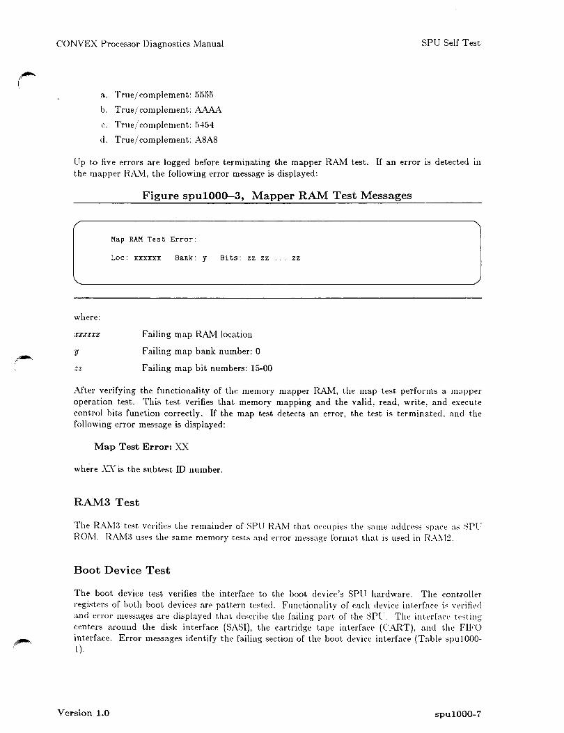
a. True/ complement: 5555
b. True/ complement: AAAA
c. True/ complement: 5454
cl. True/ complement: A8A8
Up to five errors will be logged before aborting the RAMl test. This permits isolated bit failures to be distinguished from gross failures (such as output shorts). The RAM error message has the following format:
spul000-4 Version 1.0
~ )
ti"""" I
I~ '
CONVEX Processor Diagnostics Manual
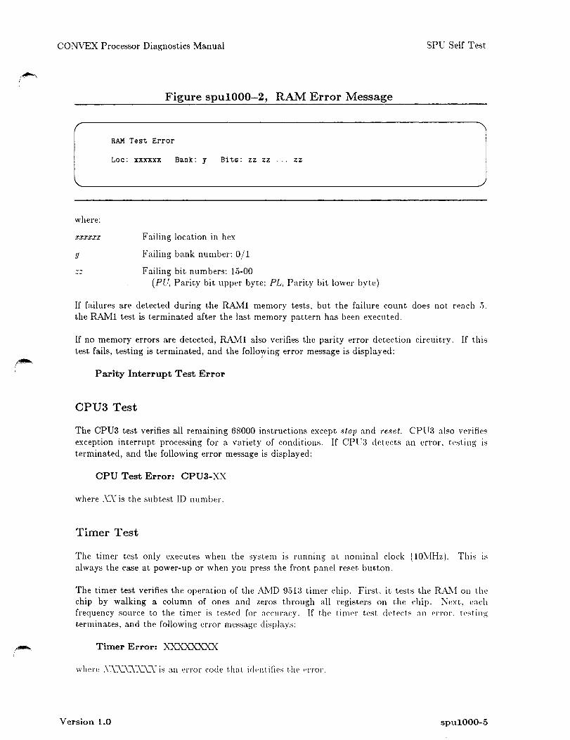
where:
:rxx:rxx
y
Figure spul000-2, RAM Error Message
RAM Test Error
Loe: xxxxxx Bank: y Bits: zz zz ... zz
Failing location in hex
Failing bank number: 0/1
Failing bit numbers: 15-00 (PU, Parity bit upper byte; PL. Parity bit. lower byte)
SPU Self Test
If failures are detected during the RANil memory tests, but the failure count does not reach .'). the RA.NU test is terminated after the last memory pattern has been executed.
If no memory errors are detected, RAMl also verifies the parity error detection circuitry. If this test fails, testing is terminated, and the follo~ving error message is displayed:
Parity Interrupt Test Error
CPU3 Test
The CPU3 test verifies all remaining 68000 instructions except stop and reset. CPU3 also verifies exception interrupt processing for a variety of conditions. If OPU3 detect.s an error. testing is terminated, and the following error message is displayed:
CPU Test Error: CPU3-XX
where _L\ is the subtest ID number.
Timer Test
The timer test only executes when the system is running at nominal clock ( lOMHz). This is
always the case at power-up or when you press the front panel reset button.
The timer test verifies the operation of the A.NlD 951:3 timer chip. First, it tests the RAM on the chip by walking a column of ones and zeros through all registers on the chip. Next, ea.ch frequency source to the timer is tested for accuracy. If the timer test detects an error. testing terminates, and the following error message displays:
Timer Error: XXXXXXXX
where _\_\_\...\...\...\...\...\'"is an error rnde that idl·ntifies the l~!Tor.
Version 1.0 spul000-5

SPU Self Test CONVEX Processor Diagnostics Manual
Console Test
The console test verifies the operation of the RS-232 port connected to the system console device. This tests only the local port, and gives no indication of the correct operation of the console device itself. First, the RS-232 port is placed in loop-back mode, allowing it to read each character that has been written to the port. All 256 possible byte values are written to and read from the port. Next, each of the interrupts on the port is tested. If the console test detects an error, testing ceases, and the following error message displays:
Console Error: XXX:XXXXX
where _\..LLLL'"Y:L~ is an error code that identifies the error.
Remote Test
The remot.e test verifies the operation of the RS-232 remote port. This tests only the remote port and gives no indication of the correct operation of the remote connection itself. The RS-2:32 port. is placed in loop-back mode and tested in the same manner as the local console. If the remote test detects an error, testing ceases, and the following error message displays:
Remote Error: XXX:XXXXX
where .XJOu'YXXXX is an error code that identifies the error.
RAM2 Test
The RANI2 test verifies all SPU RAM above ROM. It performs the following tests:
1. Address uniqueness
2. Bit functionality
a. True/complement: 5555
b. True/complement: AAAA
c. True/complement: 5454
cl. True./ complement: A8A8
As in the RAMl test, up to five errors are logged before the RAM2 test is terminated. The error message format is the same as for the R.Afv[l test.
Map Test
The map test verifies the memory mapper RAM and then tests mapper functionality. It performs the following tests on the memory mapper RA1VI:
1. Output shorts
2. Address uniqueness
:L Bit functionality
spul000-6 Version 1.0
~\
CONVEX Processor Diagnostics Manual SPU Self Test
a. True/complement: 5555
b. True/ complement: AAAA
c. True/ complement: 5454
d. True./ complement: A8A8
Up to five errors are logged before terminating the mapper RAM test. If an error is detected m the mapper RANI, the following error message is displayed:
where:
;rx:rxxx
y
Figure spul000-3, Mapper RAM Test Messages
Map RAM Test Error:
Loe: xxxxxx Bank: y Bits: zz zz ... zz
Failing map RAM location
Failing map bank number: 0
Failing map bit numbers: 15-00
After verifying the functionality of the memory mapper RAM, the map test performs a mapper operation test. This test verifies that memory mapping and the valid, read, write, and execute control bits function correctly. If the map test detects an error, the test is terminated, and the following error message is displayed:
Map Test Error: XX
where XX is the subtest ID number.
RAM3 Test
The RA1vt:3 test verifies the remainder of SPU RAM that occupies the same address space as SPlROM. RA1v1:3 uses the same memory tests and error message format that is used in rt-\i\l::!.
Boot Device Test
The boot device test verifies the interface to the boot device's SPU hardware. The controller registers of both hoot devices are pattern tested. Functionality of each device interface is YPrifit>d and error messages are displayed that describe the failing part of the SPll. The in terfaee te:-;ti ng centers around the disk interface (SASI), the cartridge tape interface (CART), and the FIFO interface. Error messages identify the failing section of the boot device interface (Table spu 1000-1).
Version 1.0 spul000-7
I '
SPU Self Test CONVEX Processor Diagnostics Manual
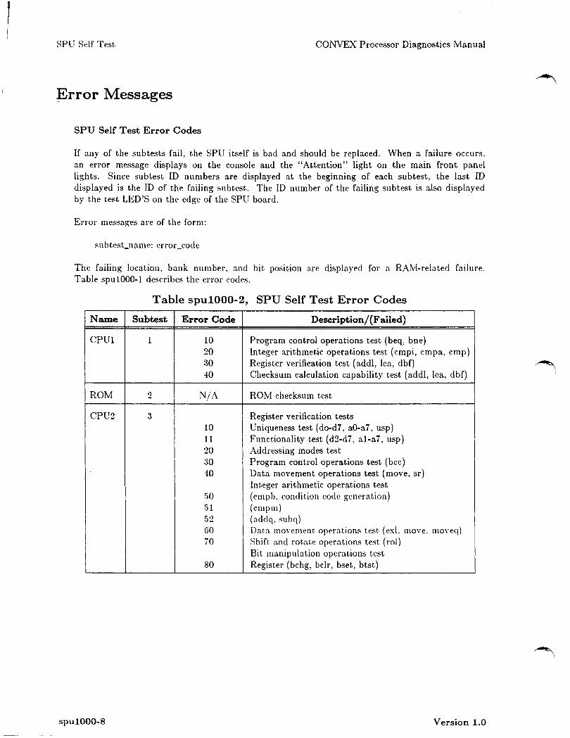
~rror Messages
SPU Self Test Error Codes
If any of the subtests fail, the SPU itself is bad and should be replaced. When a failure occurs, an error message displays on the console and the "Attention" light on the main front panel lights. Since subtest ID numbers are displayed at the beginning of each subtest, the last ID displayed is the ID of the failing subtest. The ID number of the failing subtest is also displayed by the test LED'S on the edge of the SPU board.
Error messages are of the form:
subtest_name: error_cocle
The failing location, bank number, and bit position are displayed for a RAM-related failure. Table spul000-1 describes the error codes.
Table spul000-2, SPU Self Test Error Codes
Name Subtest Error Code Description/{Failed)
CPUl 1 10 Program control operations test (beq, bne) 20 Integer arithmetic operations test ( cmpi, cm pa, cmp) 30 Register verification test ( addl, lea, dbf) 40 Checksum calculation capability test (addl, lea, dbf)
ROM 2 N/A ROM checksum test
CPU2 3 Register verification tests 10 Uniqueness test ( do-d7, a0-a7, usp) 11 Functionality test ( d2-di, al-a7, usp) 20 Addressing modes test :30 Program control operations test (bee) 40 Data movement operations test (move, sr)
Integer arithmetic operations test .50 (cmpb. condition code generation) 51 (cm pm) 52 ( adclq, subq) GO Data movement operations test, (ex!. move, moveq) 70 Shift and rotate operations test ( rol)
Bit manipulation operations test 80 Register (bchg, bclr, bset, btst)
spul000-8 Version LO
CONVEX Processor Diagnostics Manual SPU Self Test
Name
RAMl
CPU3
Timer
Console
Version 1.0
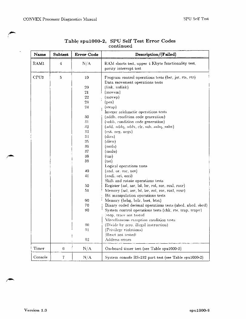
Tabl~ spul000-2, SPU Self Test Error Codes continued
Subtest Error Code Descri.ption/ (Failed)
4 N/A RANI shorts test, upper 4 Kbyte functionality test, parity interrupt test
5 10 Program control operations tests (bsr, jsr, rts, rtr) Data movement operations tests
20 (link, unlink) 21 (movem) 22 (movep) 2:3 (pea) 24 (swap)
Integer arithmetic operations tests :m (addb. rnndition code generation) :H (subb, rnndition code generation) :32 (add, addq, addx, cir, sub. subq, subx) :3:) (ext. neg, negx) :34 (divs) ;3,5 (di vu) 36 (muls) 37 (mulu) :38 ( tas) 39 (tst)
Logical operations tests 40 (and. or, eor, not) 41 (andi, ori, eori)
Shift and rotate operations tests 50 Register ( asl, asr, Isl, lsr, rol, ror, roxl, roxr) 51 Memory (as!, asr, Isl. lsr, rol, ror, roxl, roxr)
Bit manipulation operations tests GO Memory (bchg, heir, bset, btst) 70 Binary coded decimal operations tests (abed. nbcd. sbcd) 80 System control operations test.s ( chk, rte, trap. t.rapv)
[stop. trace not tested] l\Iiscellaneous exception condition tests
90 (Divide by zero. illegal inst.ruction) I n1 ( PrivilegE· violations)
[Reset not test.eclJ I
92 Address errors
G N/A On-board timer test (see Table spul000-2)
7 N/A System console RS-232 port test (see Table spul000-2)
spul000-9
SPU Self Test
Name Subtest
RAM2 9
Map A
RAM2
RAM3 B
Remote 8
CONVEX Processor Diagnostics Manual
Tabl~ spul000-2, SPU Self Test Error Codes continued
Error Code DeseriptiOn/ (Failed)
N/A RAM functionality test for all RAM above ROM address space
N/A Map RAM functionality test 00 Address translation test
Access control tests 10 (Supr R in 512KB-4 Mbyte range) 11 (Supr Win 512KB-4 Mbyte range) 12 (Supr E in 512KB-4 Mbyte range) 20 (Supr R in nonvalid page) 21 (Supr W in nonvalid page) 22 (Supr E in nonvalid page) 40 (User R in 4 Mbyte-16 ~'{byte range, uio = 0) 41 (User W in 4 Mbyte-16 Mbyte range. uio = 0) 42 (User E in 4 Mbyte-16 Mbyte range, uio = 0) 50 (User R in 4 Mbyte-16 Mbyte range, uio = 0) 51 (User Win 4 Mbyte-16 Mbyte range, uio = 0) 52 (User E in 4 Mbyte-16 Mbyte range, uio = 0) 60 (User R in non valid page) 61 (User Win nonvalid page) 62 (User E in nonvalid page) 70 (User R with read enabled) 71 (User W with write enabled) 72 (User E with execute enabled) 80 (User R with read disabled) 81 (User W with write disabled) 82 (User E with execute disabled)
N/A RAM functionality test for RANI in ROM address space
N/A Remote RS-232 port test (see Table spul000-2)
The timer and UART errors are report,ed as error codes (Table spulOOO-~).
spul000-10 Version 1.0
~ \
I~
CONVEX Processor Diagnostics Manual SPU Self Test
Table spul000-3, Timer and UART Error Codes
Timer Description
1 Timer chip registers do not match after same number of clocks.
2 After same number of clocks the counters do not match each other.
3 Error tolerance exceeded for value in counters.
UART Description
1 Loopback data does not match.
2 Timeout occurred on UART.
;3 Framing error from UART.
4 Overrun error from UART.
5 Parity error from UART.
6 Interrupt not received.
If any of the subtests fail, the SPU itself is bad. A failure is indicated by a printed message or by the Attention light on the main front panel.
Boot Devices Error Codes
The disk returns error codes to indicate a problem between the SPU and the controller board (Table spul000-3).
Version 1.0 spul000-11

SPU Self Test CONVEX Processor Diagnostics Manual
Table spu100f:t·4, Disk/~PU Error Codes
Code Description
ff ff 0001 Controller took longer than 10 seconds to go busy after selected.
ffff0002 Controller took longer than 1 second during ack/req handshake during command transfer.
ff ff 0003 Controller took longer than 1 second during ack/req handshake during data input transfer.
ff ff 0004 Controller took longer than 1 second during ack/req handshake during data output transfer.
ff ff 0005 Controller took longer than 10 seconds to give "message complete" status after command.
ff ff 0006 Controller took longer than 1 second to give "message ready" status after command.
ffff0007 Controller reported parity error.
ff ff 0008 Error occurred during error processing.
ff ff 0009 Data transfer did not complete specified length.
ffffOOOa Disk drive type specification is invalid.
ff ff OOOb Block length specified in read or write 1s not multiple of sector size.
ffffOOOc Controller took longer than 1 second to go idle.
ffffOOOd Read/write compare failed Ill
test. ffffOOOe Controller timeout without
request after drive select. ffffOOOf Controller timeout without,
request aft,er command.
The disk controller can return the following error codes:
spul000-12 Version LO
CONVEX Processor Diagnostics Manual SPU Self Test
Table spul000-5, Disk Controller Error Code Types
Error &-rop'Jcype Gode
0-6 Disk drive error codes 10-19 Disk medium error codes lA-lE Disk medium error codes 20-25 SPU command error codes 16-17 Not assigned lB,lF Not assigned 22 Not assigned 26-2F Not assigned
See Table spul000-4 for more detail.
Table spul000-6, Controller Error Codes
Gode DeSCl"iption
00 No sense. 01 No index signal. 02 No seek complete. 03 Write fault. 04 Drive not ready. 06 No track 00. 10 ID CRC error. 11 Uncorrectable data error. 12 ID address mark not found. 13 Data address mark not found. 14 Record not found. 15 Seek error. 18 Data check in no retry mode. 19 ECC error during verify. lA Interleave error. lC Unformatted or bad format on drive. ID Self-test failed. 1E Defective track (media errors). 20 Invalid command. 21 Illegal block address. 23 Volume overflow. 24 Bad argument. 25 Invalid logical unit number.
The cartridge tape unit can return the error codes listed in Table spul000-5.
Version 1.0 spul000-13
SPU Self Test CONVEX Processor Diagnostics Manual
Table spul000-7, Cartridge Tape Error Codes
Code Description
1 Drive would not go ready. 2 Drive would not recalibrate. 3 Could not seek to boot track.
The code bbbbss04 may also appear, where bbbb is the number of bytes out of 16384 that did not get transferred, and ss is defined as:
7 I
I I
I I I I I I I I .
spul000-14
Figure spul000-4, ss Definition
bit • • • , . I
I I I I I I I I I I I I I I I I I I I I .
0 I
I command busy
data request pending
lost data on transfer
CRC error detected
record not found
record type read (l=Clata deleted)
drive write protected
drive ready
Version 1.0

spu2000
SPU Peripheral Test
Introduction
Test program spu:!OOO is a dual-purpose. standalone test/utility program. It performs two funetions: peripheral test/format, and SPU UNIX root partition restores. This program does not operate under the dshell. The test/utility function formats and tests the disk and cartridge tapes. The SPU UNIX root restore function uses tapes created by /etc/backup to create a UNIX root on the Winchester or !Omega disk. This program tests the cartridge tape and disk interfaces.
Test Program Invocation
Dshell does not support this standalone test/utility program.
User Interface
One way to execute this test program is to boot a /etc/backup format tape. The backup script copies the spu2000 program to the boot location on the cartridge tape. Then. the test program boots and the first prompt displays.
You can use a faster method of executing this test program if root exists on the Winchester disk.· First, change the Cl or C120 switch to local. If SPU UNIX is running, type:
/etc/reboot<CR>
The soft front panel selection menu displays on the screen. (If SPU UNIX is NOT running, press the reset button to display the front panel menu.)
At the (fp) prompt. type:
boot<CR>
The follcwing displays:
SPU UNIX boot (Generated .)
Then enter the following:
dk(l,O)stand/spu2000
\Vhether you exernte :-;pu:!OOO from tape or disk. the first-level prompt present,.; !'om options. ;i.,.;
."hown in the following figure:
Version 1.0 spu2000-1

SPU Peripheral Test CONVEX Processor Diagnostics Manual
Figure spu2000-1, Peripheral Test Selection
SPU Disk/Tape Diagnostic Utility $Revision: 1.3 $
(U) for UNIX Root Restore (D) for Disk/Tape Utility (S) for SPU Hardware Utility (R) for Reboot SPU
Enter utility to execute -
(NOTES)
• Entering U restores the UNIX root.
• Entering D displays the disk/tape utility menu (see "Disk/Tape Format/Test Function").
• Entering S displays the menu for the SPU hardware utility.
• Entering R simulates a reset to the SPU and returns control of the SPU back to the EPROM code.
UNIX Root RESTORE Function
Once you enter this mode, the program reads and displays the date of the backup.
Figure spu2000-2, UNIX Root RESTORE Function Display
SPU UNIX Root Partition Restore reading bad block table ...
Attempting sector: o Successful. reading root date code ...
Attempting sector: O Successful.
SPU UNIX root size= 2052 blocks. Backed up Mon Aug 19 21:48:39 1985
After the backup date displays, the function asks whether to restore to a disk (Winchester) or IOrnega disk.
spu2000-2 Version 1.0

CONVEX Processor Diagnostics Manual SPU Peripheral Test
Restore root onto disk or !Omega? [di] (d) Define the device to recover
. ~\
Then it asks you to input disk parnmeters (or use defaults) for the selected disk display (see "Disk/Tape Format/Test Function). Finally, t.he screen prompts for restore permission. You can select either 0 or 1 for the recovery copy of the root from the tape.
Recover the root at this time? [yn] (n) Recover copy o or !? (01] (O)
.... '('.&.~\. ?·hJ . ('! ~ > ;: ./.. I ../- . • :::>..,.. u e.t,..(.... (' ~ ~ ~
Disk/Tape Format/Test Function
When you select d as the peripheral test selection, the di.~k/tape menu displays as follows:
Figure spu2000-3, Disk/Tape Format/Test Function Display
SPU Disk/Tape Utility
(D) for Disk (SPU Winchester) (T) for Tape (SPU cartridge) (I) for !Omega (SPU removable disk) (E) for Exit Test
Enter controller type/function -
(WARNING)
Please be careful when entering responses. as the format utility is data destructive.
To return to t.he main level prompt., enter E; otherwise. t•nter your selection for disk. tape. or Iomega. Entering D, T. or I prompts you wid1 t.he following:
Format desired using standard defaults and no prompts [yn] Cy)?
If you reply y, you are given the opportunity to change your answer as the following prompt displays:
ALL PREVIOUS DATA WILL BE DESTROYED. ARE YOU SURE [yn] (n)?
Replying y begins a format of the device without requiring any further interYetHion. \\"ht>n t hl' format finishes, the following prompt displays, asking whether you wish to do another format:
Format another with defaults and no prompts [yn] (n)?
Version 1.0 spu2000-3

SPU Peripheral Test CONVEX Processor Diagnostics Manual
If you reply y, the automatic format operation repeats. Answering n, returns you to the mam level prompt.
If you answer the first question Format desired using standard defaults and no prompts) with n, you are prompted for disk information. If you are using a Winchester (disk) or !Omega, the following disk parameter prompts display with the default shown in parentheses.
Figure spu2000-4, SPU Winchester Disk Parameters Display
SPU Winchester Disk Parameters:
Number of heads --------Number of cylinders ----Start of write precomp -Step rate --------------Sector data size -------Sectors per track/head -Logical drive number ---Sector interleave -------
(6)
(320) (128) (2)
(512) (18)
(0)
(3)
Are all inputs correct? - [yn] -> y
-> -> -> -> -> -> -> ->
The optimum parameters (see Table spu2000-1) have been initialized in the program and are recommended as the defaults to the questions. (Although you do have the option to change these parameters, it is not recommended.)
If you use a tape, the optimum parameters display, but you cannot change them.
The next prompt displays:
Format/test. Debug. or Abort operation [F.D,A]?
The abort operation option returns you to the main prompt. level; whereas. the formafife.st option moves you to the .mbte.st enable prompts. which a.re illustrated in Figure spu:.W00-2. (.\t this time. the debug option is nonfunctional and returns you to t.he menu.)
Table spu2000-1, SPU Disk/Tape Format Defaults
Parameter Tape Winchester Iomega
Number of heads 6 6 1 Number of cylinders 251 320 306 Start of write precomp N/A 128 0
Step rate N/A 2 0 Sector data size 102-1 512 512 Sectors per track/head 17 18 6-1
Logical drive number 0 0 0 Sect.or interlt'ave l ;3 l(j
spu2000-4 Version 1.0

CONVEX Processor Diagnostics Manual SPU Peripheral Test
Subtest Enable
You can enable each subtest separately. The tests selected can be looped on. and the maximum number of errors allowed can be modified. The test prompts display one at a time as shown in Figure spu2000-2.
Figure spu2000-5, SPU Peripheral Test Prompts
Run maintenance track test.? -- [yn] (n) -> Run format. test.? ------------- [yn] (n) -> Run write test.? -------------- [yn] (n) -> Run read test.? --------------- [yn] (n) -> Run bad block fix? ----------- [yn] (n) -> Run random read test.? -------- [yn] (n) -> Run seek test.? --------------- [yn] (n) -> LOOP ON TESTS? --------------- [yn] (n) -> MAX NUMBER OF ERRORS? ------------- (1) ->
Are all inputs correct.? - [yn] ->
Run these tests only in the order shown. You must select a write test before a read test can be attempted because the read test performs a 'data compare' using the pattern the write test generates.
SPU Hardware Utility
The SPU hardware utility functions the same as spuuti'l (see SPU UNIX Utilitie.s lvfanual) but. with reduced capability due to its standalone operation.
(NOTE) This ut.ility is menu driven and is not. to be used by an~·one except qualified CONVEX employl'es.
Class Descriptions
Because this test is all one class, no class selections are provided.
Subtest Descriptions
The following paragraphs describe the spu2000 subtests in execut.ion order, according to t.he peripheral test prompts as illustrated in Figure spu2000-S.
Version 1.0 spu2000-5

SPU Peripheral Test CONVEX Processor Diagnostics Manual
Maintenance Track Subtest
This subtest applies to IOmega disks only. It displays the data stored on the maintenance track and allows changes in some areas. The data that displays consists of five parts, as follows (Figure spu2000-3 shows an example of the maintenance track subtest display):
Bad track log Indicates all tracks flagged as bad, along with the number of the alternate track being used.
Auto stop of spindle Specifies the amount of idle time before stopping the spindle. The time displayed is the time the drive remains spinning while not in use. The purpose of stopping the spindle is to prevent excessive wear of the media under the read/write head.
Write verify flag Provides for automatic read of any written sector and performance of a CRC check when the flag is y. Setting of the flag causes a slowdown of the 1/0 since each time a track is written, a second revolution of t.!1e disk is required to verify the written blocks. This technique, however, provides the advantage of detecting a write error at write time, which allows a retry of the write operation.
ECC checking flag Provides for automatic calculation of an ECC for the entire track whenever one or more sectors on a track are written-if the flag is y. Each time data is written to a track, the entire track must be read to recompute the ECC, and then the ECC block must be written. This can require as many as three revolutions of the disk. Having the flag set at y provides the capability to correct unrecoverable read errors. The ECC can recover an entire 256-byte block which has become unreadable.
Interleave value
spu2000-6
Indicates the number to be added to the last sector number. This number indicates the next consecutive sector to be used for a read or write operation. Interleaving sectors allow processing time between reads or writes. If set properly, the next desired sector should be coming under the read/write heads very shortly after processing of the last sector is completed.
Version 1.0
~ I

""" \
CONVEX Processor Diagnostics Manual SPU Peripheral Test
Figure spu2000-6, Maintenance Track Data Display
Running Maintenance track subtest
MAINTENANCE TRACK DATA
Bad Track Log: bad replacement track track
No bad tracks have been flagged
Other Data: Idle time before auto stop of spindle (minutes) -----> 5 Write verify --------------------------------------> y Check ECC -----------------------------------------> y Interleave ----------------------------------------> 8
Change maintenance track data [yn] (n)? n
You can change any of the maintenance data except the bad track data. If you change the ECC flag to y or change the interleave value, a format .5ubtest automatically runs (whether you specified it or not). This is necessary to make the disk usable. If ECC is already set to y, the format subtest does not execute (unless you enabled it). The following figure shows an example of the input screen for the Maintenance Track Subtest.
Figure spu2000-7, Changing Maintenance Track Data
Change maintenance track data [yn] (n)? y Idle time before auto stop of spindle (minutes)
[5/7.5/10/ ... /30/d (for disabled)] (5) -> Write verify
[y/n] Check ECC (Disk will be reformatted if change to 'y')
[y/n] Interleave (Disk will be reformatted if change)
[1/2/4/8/16/32]
WARNING - THE DISK WILL BE REFORMATTED!
Are all inputs correct [yn]? y
Version 1.0
maintenance track ~hange underway
Maintenance track subtest -------> passed Running Format subtest ------------------> passed
(y)
(n)
(8)
0:00:25 0: 01: 30
->
->
16
spu2000-7

SPU Peripheral Test CONVEX Processor Diagnostics Manual
Format Subtest
This test formats Winchester, !Omega, or cartridge tape media. The test uses the format parameters selected or the defaults from the Maintenance Track Subtest, with one exception. If an !Omega is being formatted and the interleave value was changed in the previous Maintenance Track Subtest, then that interleave value is used during formatting.
When an IOmega is being formatted and either a NO TRAC[( 0 or NO INDEX SIGNAL error occurs. the message:
Reinsert disk cartridge. Press 'return· when ready
displays. Reinserting the disk and pressing the return forces the IOmega controller to reread the maintenance t.racks in hopes that another attempt will succeed. If one of these two errors still occurs on the second read, the following message displays:
Error-maintenance tracks on !Omega cartridge may be bad Rebuilding these tracks results in loss of the current bad track history Rebuild maintenance tracks [yn] (n)
Rebuilding the maintenance tracks may allow the disk to be usable again.
Write Subtest
The write test repeats a fixed pattern, Oxe5a55a5e, the number of times necessary to fill a block. This is written to every block which the drive parameters indicate exist. For instance, if only 100 tracks are specified on a 306 track !Omega, then only the first 100 tracks are written.
Read Subtest
This test reads each block which the drive parameters indicate exist and compares ea.ch block with the fixed pattern, Oxe5a55a5e. The test keeps all blocks that generate errors in an internal table. These blocks are marked as bad during the Bad Block Fix Subtest so they will no longer be used.
Bad Block Fix Subtest
When this test begins, you a.re prompted to enter manually the number of ea.ch bad block (if any) that you a.re aware of that was not previously flagged by the Read Subtest as being bad. Then the test sorts the blocks into ascending order and writes them to the disk/t.ape. After the blocks are logged on the disk/tape, they are no longer available for data storage. Instead. alternate blocks are used.
Random Read Subtest
This test performs 100 reads to randomly calculated block numbers. Before the test begins. the test determines t.he maximum number of blocks on the disk. Block numbers are ealculated in tlw rangt· zero to tht· maximum minus one.
spu2000-8 Version 1.0

CONVEX Processor Diagnostics Manual SPU Peripheral Test
Seek Subtest
This seek test performs an accordion seek in reverse. A seek is made from mi"n to max track, then to min+l, max-1, min+2, max-2, etc. The accordion seek ends with a one-track seek. Each time the head comes to rest on a track, the test reads the middle block of the track to verify that the seek was successful.
Other Subtest Options
The final two options, as shown in Figure spu2000-2, allow you to specify looping on tests and/or to specify the maximum number of errors that can occur before testing is aborted. Please note t.!rnt. if you choose looping, t.he tests loop indefinitely, unless one of the following conditions occur:
1. You press a CTRL-A, which returns you immediately to the main menu. Since this action may leave the drive in an unknown state, you should use the alternative described in condition 2.
2. You press either CTRL-B or CTRL-C, which terminates the test in a controlled manne1·. Thus, a few seconds may pass before this termination actually occurs. If a format was in process, the subtest must complete before termination occurs.
3. The test reaches the maximum number of errors which causes test termination.
Execution Time
The following times are maximum under nominal conditions:
Table spu2000-2, Test Execution Time
Subtest Number of Minutes
Tape Disk lOmega
Main. Track N/A N/A 1.0 Format 10.0 1.5 1.5 Write 10.0 9.5 17.0 Read 20.0 11.0 10.0 Bad Block Fix 0.5 1.5 1.5 Random Read N/A 0.5 0.2 Seek N/A 1.5 0.8
Total 40.5 25.5 32.0
Error Messages
Spu2000 reports I/O errors in a standard format. However, if additional data ifi available at tlw time of the error, that data is also reported. The basic format for the errors follows:
spu2000· <error desc> on <device> drive <dev #> during command <command> Operation <operation type> [optional data displays here and on next line]
Version 1.0 spu2000-9

SPU Peripheral Test CONVEX Processor Diagnostics Manual
where: ~,
<error desc> Describes the type of error that occurred, such as, NO INDEX SIGNAL, DRIVE NOT READY, SEEK ERROR.
<device> Is one of the following: Adaptec, !Omega, or Tape.
< dev .# > Specifies the device number. Each device begins at 0 with additional drives of the same type being numbered l, 2, ....
<command> Identifies the I/O command to the drive which resulted in the error; for example, READ SECTOR, WRITE SECTOR, REZERO UNIT, SEEK
<operation type> Provides the name of the subtest, such as, Format, Read, Bad Block Fix, Disk Restore, Seek.
[optional data] reports the block being accessed if using a disk (Adaptec or !Omega) and a read. write, or verify is underway.
Tlw stream. segment.. and sector is printed if using a tape and the error is detected by the controller or a data compare error was det.ected by the SPU.
A third line is printed. which contains the position of the error within the block (or sector on tape), the expected data, and the actual invalid data when using either a tape or disk and a data compare error occurs.
Examples of error messages that can occur are:
spu2000 NO INDEX SIGNAL on Iomega drive 0 during command REZERO UNIT Operation: Format
spu2000 ID CRC ERROR on tape drive 0 during command READ SECTOR. Operation: Read Stream: 3 Segment: 142 Sector: 14
spu2000 DATA COMPARE ERROR on Adaptec drive 1 during command READ SECTOR. Operation Read Block: 4523 Bytes into block: 24 Expected OxE5A55A5E Actual: OxOOOOOOOO
spu2000: ID CRC ERROR & RECORD NOT FOUND on tape drive 0 during command WRITE SECTOR. Operation Write Stream 1 Segment 200 Sector: 5
Notice that the last error message reports more than one error. The tape controller sets a st>ries of bits to indicate which errors have occurred. The error message for each error prints,
Error Descriptions
This section provides an alphabetical list of errors reported by spu2000, with a brief description of the error.
BAD ARGUMENT
Peripheral: Winchester
The Adaptec Winche:-;t.er drive detected a bad value in one of the fields of a command block.
spu2000-10 Version 1.0

~ I
CONVEX Processor Diagnostics Manual SPU Peripheral Test
BAD SEEK
Peripheral: Winchester, !Omega
The disk drive was unable to find the requested track.
COMMAND TIMEOUT
Peripheral: Tape
The tape drive has taken an excessively long time performing a head load, seek. or head positioning.
DATA ADDR MARK NOT FOUND
Peripheral: Winchester, !Omega.
Each time a sector is written. a fixed pat.tern is writt.en just before the sector: this is called the data address mark. If this pattern is not detected when an attempt is made to read the sector back, the drive has no idea where the data begins. Thus, the drive reports a data address mark not found.
DATA COMPARE ERROR
Peripheral: Winchester, !Omega, Tape
Data just read does not match with an expected data pattern (see sections 4.4 and 4.5 ). The data in error is printed.
DATA CRC ERROR
Peripheral: Winchester, !Omega, Tape
At write time, the Cyclic Redundancy Check (CRC) algorithm combines all the bytes in a sector and generates a 2-byte field which is written after the data. Upon read back, the bytes being read are a.gain combined. u:3ing the :'>a.me algorithm. and the result. is compared with the 2 bytes at. the encl of the data. If the bytes do not mat.ch. this error occurs.
DATA XFER NOT COMPLETE
Peripheral: !Omega
The sector buffer in the drive either was not completely written to the disk or was not completely transferred to the SPU when reading from the disk.
Version 1.0 spu2000-11

SPU Peripheral Test CONVEX Processor Diagnostics Manual
OMA TIMEOUT
Peripheral: !Omega
Transfer of data to or from the !Omega's internal memory by the !Omega's direct memory access controller failed.
DRIVE ALREADY BUSY
Peripheral: Tape
The SPU is about to perform an I/O operation to the t.ape but finds that the tape controller is busy doing an unrequested operation.
DRIVE NOT READY
Peripheral: \iVinchester, !Omega, Tape
The peripheral is not ready to perform any I; 0 operations. This error generally occurs with the cartridge tape, although it can occur from any of the peripherals. Once a tape has been inserted. it takes a ma.ximum of 3 minutes for the tape to reposition itself. The error message displays if a test was started on the tape several seconds before the tape was inse1·ted, and the tape did not go ready before the timeout.
ECO ERROR DURING VERIFY
Peripheral: Winchester
The drive is unable to correct an error using the Error Correction Code.
FIFO WOULD NOT EMPTY
Peripheral: Tape
The First In-First Out {FIFO) data buffer on the tape controller was not empty at the completion of an I/O operation.
ID ADDR MARK NOT FOUND
Peripheral: Winchester, !Omega
The drive writes a fixed pattern at the beginning of each ID {header) called the ID address mark. Each time the controller reads or writes a sector, it checks this address mark for validity first. Since the controller automatically performs retries, multiple bad reads of an ID address mark have already occurred before this error is reported.
ID CRC ERROR
Peripheral: Winchester, Tape
The checksum calculated during the read ol' an ID does not mat.eh the Cyclic Redunda1H·y Cheek sum that follows the ID. This error only prints wlwn a.II multiple retries t,o read the ID !'ail.
spu2000-12 Version 1.0
CONVEX Processor Diagnostics Manual SPU Peripheral Test
ILLEGAL BLOCK ADDRESS
Peripheral: Winchester, !Omega
The drive was sent a block (sector) address outside the valid range for the peripheral.
ILLEGAL INTERLEAVE
Peripheral: Winchester, !Omega
An interleave factor other than 1, 2, 4, 8, 16, or 32 was requested for the !Omega. For the \\.inchester, an interleave less than one or greater than 17 was requested.
INSUFFICIENT CAPACITY
Peripheral: IOmega
No room remains to store data; the !Omega is full.
INVALID BLOCK NUMBER
Peripheral: Tape
The controller detected an attempt to perform 1/0 to an invalid block on the cartridge tape. Valid block numbers must be 0 to 25601.
INVALID COMMAND
Peripheral: Winchester, I Omega
The drive controller received an unrecognizable I/O command.
INVALID LOGICAL UNIT NO.
Peripheral: Winchester
An attempt was ma.de to access a vVinchester drive whieh does not exist.
INVALID STREAM NUMBER
Peripheral: Tape
An aUempt was made to write to a stream number other than 1 - 6.
LOST DATA
Peripheral: Tape
The host sent data too rapidly to the tape controller causing a loss of some of the data.
Version 1.0 spu2000-13
SPU Peripheral Test CONVEX Processor Diagnostics Manual
MEDIA NOT LOADED
Peripheral: !Omega
This error occurs when the cartridge is not loaded with the door securely closed and an I/O attempt is made to an !Omega cartridge.
NO INDEX SIGNAL
Peripheral: Winchester, !Omega
The media is not spinning at the correct speed, or it is not spinning.
NO SEEK COMPLETE
Peripheral: Winchester
The drive detect.s a bad seek.
NO TRACKO
Peripheral: Winchester, !Omega
On the Winchester, this message indicates a seek to track zero failed. For the !Omega, it means the maintenance track data (all 8 copies) is bad.
RECORD NOT FOUND
Peripheral: Winchester, !Omega, Tape
The ID field for the requested block could not be found. Generally, this means 1/0 errors are preventing the ID from being read.
UNCORRECTABLE DATA ERROR
Peripheral: Winchester, IOmega
An error in the data field of a block was detected. Either the ECC correction was not enabled or the error was too large for ECC correction to recreate the data.
UNFORMATTED OR BAD FORMAT
Peripheral: Winchester
The Winchester drive controller detected a flawed format and aborted the current 1/0 operation.
VOLUME OVERFLOW
Peripheral: Winchester
The disk is full: there is no room Lo store aclclitiona.I data.
spu2000-14 Version 1.0
~ I

CONVEX Processor Diagnostics Manual SPU Peripheral Test
WRITE FAULT
Peripheral: Winchester, I Omega
An internal drive error resulted in an inability to complete the requested write operation. This error will occur if the automatic write verify is turned on and the verify fails.
WRITE PROTECTED
Peripheral: !Omega, Tape
An attempt was made to write to an !Omega or tape cartridge that is write protected.
Version 1.0 spu2000-15

SPU Peripheral Test CONVEX Processor Diagnostics Manual
THIS PAGE INTENTIONALLY LEFT BLANK
spu2000-16 Version 1.0

~· I
~
spu4000
SPU Kernel Test
Introduction
The SPU kernel test verifies the interface between the Service Processor llnit (SPU) and the Cl or Cl20, as well as a portion of the remaining Cl or Cl20 subsystems. The kernel test is designed to verify the hardware in a hierarchical, bottom-up fashion. The eight distinct levels of the kernel test are:
1. SPU Control Register Integrity
~. DBUS Interface
:3. Board Identification
4. Scan Ring Integrity
5. Hard-Error Capability
6. Power and Clock Margin
i. PBUS Integrity
8. PBUS Interrupt Bus Integrity
The kernel test interfaces with as few of the unique features of the CONVEX board architectures as possible. Test points are chosen close to the edge of the board in order to minimize impact of the board on the test.
Spu4000 relies on the integrity of the SPU. It should be run after the SPU and its peripherals have been verified by the SPU Self-Test. When the kernel t.est. completes, it is possible to proceed to other functional tests of the Cl or Cl20 with confidence that the SPU and the major system interfaces are operational.
Test Program Invocation
Spu-1000 supports all the features of the d.shell. BecaUSl' spu-1000 Hrifies t.he computer ·s ab iii t>· to perform a system reset, this test should not be initiated uc;ing a sysreset or initall com1mmd.
Use the following procedure to invoke .spu400.
Version LO spu4000-1

SPU Kernel Test CONVEX Processor Diagnostics Manual
Figure spu4000-1, Test Invocation
(spu)> cd /mnt/test (spu) > dshell
test spu4000 [-c [class number(s)]] [-s [subtest numbers (s)]] [ +> filename
where the arguments enclosed by [ ] are optional. Entering only the test name (spu4000) executes all spu4000 subtests. AB each subtest is designed to be independent of all other subtest,s, you can execute a specific class(es) of subtest(s) or one or more individual subtests by using the -c or -.s options, respectively. (For more information on using these options refer to the "Dshell and Scan Overview" chapter.) The [ +> filename] option ensures that all test results are placed in filename.
The first phase of the test program requests information conCl'rning hardware rnnfiguration and scan operation display. The initial test query:
Use Default Test Parameters? [y/n]
allows you to select the default values for the configuration and scan operat.ion display. The default configuration is determined by examining the board configuration file. This file contains the boards present in the system. Spu4000 determines the CCU and NI.AU slots that contain boards. An affirmative response to this query selects the default configuration (any IOP and NI.AU detected by scan) and disables the scan operation display. (A severely defective board may not be detectable by scan and would, therefore, not be tested.
If you give a negative response, the SPU Kernel Test prompts you for the configuration of ea.ch 1/0 and memory board, as illustrated in Figure spu4000-1. It also queries whether you wish to enable the display of the scan operations. Since the scan enable p"roduces large volumes of output, this option is useful only to an operator experienced in scan ring operations. Normally you should accept the default n (off).
spu4000-2 Version 1.0
--- --

r
CONVEX Processor Diagnostics Manual SPU Kernel Test
Figure spu4000-2, Test Parameter Menu
DEFINE TEST PARAMETERS
[] Encloses allowed ranges or values () Encloses default
Moves to previous prompt or aborts input :nn Moves to prompt nn; 0 aborts input
Moves to first unsatisfied prompt
1: Use Default Test Para.meters? [y/n] Cy) ->n 2: Test Boa.rd Type: CCU1? [y/nl Cn) -> 3: Test Board Type: CCU2? [y/n] (n) -> 4: Test Board Type: CCU3? [y/n] (n) -> 5: Test Boa.rd Type: CCU4? [y/nl (n) -> 6: Test Boa.rd Type: CCUS? [y/nl (n) -> 7: Test Board Type: CCU6? [y/nl (n) -> 8: Test Boa.rd Type: CCU7? [y/nl Cy) -> 9: Test Board Type: MAUQ? [y/n] (y) ->
10: Test Board Type: MAU1? [yin] (n) -> 11 : Test Boa.rd Type: MAU2? [y/nl (n) -> 12: Test Board Type: MAU3? [y/n] (n) -> 13: Test Board Type: MAU4? [y/nl (n) -> 14: Test Boa.rd Type: MAUS? [y/n] (n) -> 15: Test Board Type: MAU6? [y/n] (n) -> 16: Test Boa.rd Type: MAU7? [y/n] (n) -> 17• Display Scan Information? [y/n] (n) -> 18: Input OK, or to question :nn ? [OK] (OK) ->
The test menu displays possible options inside brackets [ ] , separated by slashes. Default options are displayed inside parentheses ( ) and can be selected with a carriage return. You may return to a preceding question by entering A< CR> or by entering a colon followed by the question· number (:6). If you need to abort the input, enter :0.
After you have entered all the test parameters, the program logs them out again for verification. If standard output is directed to a disk file. the logged values appear there as well.
Class Descriptions
The SPU kernel tests are divided into eight classes:
Version LO spu4000-3

SPU Kernel Test CONVEX Processor Diagnostics Manual
Table spu4000-1, SPU Kernel Test Classes
Class Name Description
1 SPU Control Registers Verifies diagnostic con-trol registers
2 DBUS Interface Verifies MSB/LSB of scan rmgs
3 Board ID Test Verifies board ID by slot location
4 DBUS Integrity Verifies scan rmg integrity
5 Hard-Error Test. Verifies generation/ reporting of hard-error
6 Margin Test Verifies power/clock margin capability
7 PBUS Integrity Verifies PBUS operation
8 PBUS Interrupt Bus Integrity Verifies PBUS IB opera-ti on between the SPU, MCU and ASU
Subtest Descriptions
The following table shows the order of subtest execution, as well as maximum execution times under nominal conditions.
Table spu4000-2, Subtest Execution Order and Time
Subtest Class Description Time (mm:ss)
100 1 SPU Control Register Rebound <:01
200 '> .... SPU DBUS Loopback <:01 201 2 ASU Scan I/F . :01 202 2 ATU Scan I/F . :01 203 2 IPU Scan l/F . :01 204 2 MCU Scan I/F . :01 205 2 PCU Scan I/F < :01 206 2 VCU Scan I/F <:01 207 2 VPU 0 Scan I/F <:01 208 2 VPU 1 Scan I/F <:01 209 2 CCU 1 Scan I/F <:01 210 2 CCU 2 Scan I/F <:01 211 2 CCU :3 Scan I/F :01 212 2 CCU 4 Scan I/F <:01 213 2 CCU 5 Scan I/F <:01 214 2 CCU 6 Scan I./F <:01 215 2 CCU 7 Scan I/F :01
spu4000-4 Version LO
~ I

CONVEX Processor Diagnostics Manual SPU Kernel Test
Version 1.0
Table spu4000-2, Subtest Execution Order and Time continued
Subtest Class Description Time (mm:ss)
300 3 SPU COP <:02 301 3 ASU COP <:02 :302 3 ATU COP <:02 303 3 IPU COP <:02 :304 3 MCU COP <:02 :305 3 PCU COP <:02 306 3 VCU COP <:02 307 ;3 VPU 0 COP <:02 :308 3 VPU l COP <:02 :309 3 CCU 1 COP <:02 310 3 CCU 2 COP <:02 311 ;3 CCU 3 COP <:02 :312 ;3 CCU 4 COP <:02 ;31;3 3 CCU 5 COP <:02 ;314 ;3 CCU 6 COP <:02 ;315 3 CCU 7 COP <:02 316 3 :NIAU 0 COP <:02 317 3 MAU 1 COP <:02 318 3 MAU 2 COP <:02 319 3 MAU 3 COP <:02 320 3 MAU 4 COP <:02 321 3 MAU 5 COP <:02 322 3 MAU 6 COP <:02 323 3 MAU 7 COP <:02
401 4 ASU Scan Ring Integrity <:01 402 4 ATU Scan Ring Integrity <:01 403 4 IPU Scan Ring Integrity <:01 404 4 MCU Scan Ring Integrity <:01 405 4 PCU Scan Ring Integrity <:01 406 4 VCU Scan Ring Integrity <:01 407 4 VPU 0 Scan Ring Int.egrit.y ::Ol 408 4 VPU 1 Scan Ring Integrity '' :01 409 4 CCU 1 Scan Ring Integrity :~ :01 410 4 CCU 2 Scan Ring Integrity ':01 411 4 CCU :3 Scan Ring Integrity ._::._:01 412 4 CCU 4 Scan Ring Int.egrity <.:_:01 413 4 CCU 5 Scan Ring Integrity <:01 414 4 CCU 6 Scan Ring Integrity <:01 415 4 CCU 7 Scan Ring Integrity <:01
spu4000-5

SPU Kernel Test CONVEX Processor Diagnostics Manual
Table spu4000-2, Subtest Execution Order and Time continued
Subtest Class Description Time (mm:ss)
501 5 ASU Hard Error <:01 502 5 A TU Hard Error <:01 503 5 IPU Hard Error <:01 504 ,5 MCU Hard Error <:01 505 5 PCU Hard Error <:01 506 5 VCU Hard Error <:01 507 5 VPU 0 Hard Error <:01 508 5 VPU 1 Hard Error <:01 509 5 CCU 1 Hard Error <:01 510 5 CCU 2 Hard Error <:01 511 5 CCU 3 Hard Error <:01 512 5 CCU -1 Hard Error <:01 51:3 5 CCU 5 Hard Error <:01 51-1 5 CCU 6 Hard Error <:01 515 5 CCU 7 Hard Error <:01
600 6 Check references and SMB <:02 601 6 Check PS 1 <:02 602 6 Margin PSl low <:02 603 6 Margin PSl high <:02 604 6 Check PS 2 <:02 605 6 Margin PS 2 low <:02 606 6 Margin PS 2 high <:02 607 6 Check PS 3 <:02 608 6 Margin PS 3 low <:02 609 6 Margin PS 3 high <:02 610 6 Check clocks <:02 611 6 Margin clocks low <:02 612 6 Margin clocks high <:02 613 6 Margin clocks extender <:02
700 7 PBUS I/F Rebound ·<:02 701 7 SPU-MCU Transfers < :-15 702 7 MCU-SPU Transfers < :02
800 8 SPU-MCU Interrupts ', :01 801 8 MCU-MCU Interrupts <:01 802 8 SPU-SPU Interrupts <:01 803 8 SPU-ASU Interrupts <:01 804 8 ASU-SPU Interrupts <:01
The following paragraphs describe a basic test for each class. vVithin a given cla.-;s. all the subtests are the .same. The individual subtests differ only in which board (or board slot.) is tested.
spu4000-6 Version 1.0

CONVEX Processor Diagnostics Manual SPU Kernel Test
SPU Control Register Test
The SPU control register t.est verifies those registers on the SPU that are directly read/writable. The registers are checked wit,h an alternating ones-and-zeros pattern and then an alternating zeros-and-ones pat.tern. The registers verified by this subtest are (in the order specified):
1. RHR - Run/Halt Register
2. ECR - Event Count Register
:~. DCR - Diagnostic Control Register
4. SRR - System Reset Register
;). CMR - Clock ivlask Register
6. CGR - Clock Gate Register
1. SDR - Scan Data Register
8. MCR - Margin Control Register
9. TRH - Test Result Hegiskr
10. CPR - Control Panel Registt>r
DBUS Interface Test
The DBUS interface test verifies the capability of the SPU to communicate to the various boards over the diagnostic bus (DBUS). First it verifies the SPU's interface to the DBUS via the loopback capability of the SPU, and then it tests the DBUS interface for all the boards specified during the tiser query (Figure spu4000-2).
The SPU loop-back test checks the SPU interface to the DBUS with a walking-ones pattern Ill
both scan directions. During testing, the scan count is varied from 1 to 15.
The remaining boards are tested by checking the least significant bit (LSB) and most significant bit (MSB) of each scan ring. A one and zero are written to the two bit-positions of the ring under test. The subtest writes the MSB of the ring by shifting to the right and reading from the left, and then writes the LSB of the ring by shifting to the left and reading from the right.
Board ID Test
The board CD kst verifies the contents of t.!1e CD register from a specified board. [t reads the built.- in boa.rd identification register (COP) which was programmed when the board was manufactured, and t.hen verifies the part number of the board against valid part, numbers for the slot location.
Scan Ring Integrity Test
The scan ring integrity test verifies the integrity of each board's scan ring. The SPlT walks a one pattern and then a zero pattern around each scan ring from right to left, and then from left to right. If a failure occurs in either direction, the subtest attempts to isolate the failure by writing in the direction last written. then reading back in the opposite direction. This proce,.;s is n'1wated in innea,.;ing increnwnts until the failure is detected. If the entire ring is ret.ested without tlw fault~· hit posit.ion being found. the subtest. reports that the fault. could not be i,.;ola.kd.
Version 1.0 spu4000-7

SPU Kernel Test CONVEX Processor Diagnostics Manual
Hard-Error Recognition Test
This test verifies that each board in the system is capable of sending a hard-error interrupt to the SPU, and that the SPU correctly responds to the error. Hard-errors are generated via a set of scan operations to the board under test. The hard-error recognition test verifies the results via the interrupt status register (ISR) and the error source register (ESR). This test also checks the ISR to verify that the hard-error bit is set, and the ESR to ensure that the error bit corresponding to the board under test is set.
Power and Clock Margin Test
The margin test verifies the ability of the SPU to margin the power supplies and the system clock rate. When verifying a power supply. the subtest uses the margin control register to set the power supplies to each of the following st.ates:
1. Nominal
2. Low
3. High
For each state, the subtest. measures the voltage using an A/D converter located on the SPU, and then verifies that the voltage of the supply is within a 10% tolerance for the condition under test.
For system clock margining, the subtest uses the margin control register to select each of the following conditions for the system clock rate:
1. Nominal
2. Low
3. High
4. Extended
For each condition, the subtest sets up the interval timer to count the number of clocks received from a reference clock source. The system clock frequency is then computed and checked that it is within a 5% tolerance.
PBUS Integrity
The PBUS int.egrity test verifies t.he following:
1. The ability of the SPU to rebound patterns to its PBUS map registers (Pl'vfAP)
2. The ability of the SPU to send data/commands to the MCU over the PBUS
3. The ability of the SPU to receive data over the PBUS from the MCU
PBUS I/F Rebound
The PBUS I/F rebound test verifies the SPU's internal link to the PBUS. It does not perform PBUS transfers, but sends data to the PBUS map (PMAP), which is memory mapped in the 1/0 :-;pace of the SPU. The dat.a is then read back and verified. The patterns used include: a.lt.ernating one:-;-and-zeros. alternating zeros-and-ones. and a11 increment.ing pat.tern.
spu4000-8 Version 1.0

CONVEX Processor Diagnostics Manual SPU Kernel Test
The subtest also verifies the memory-parity detection circuitry by writing a pattern to the PMAP with the "force bad parity" bit set. Memory is read and checked for the correct SPU bus-error indication.
SPU - MOU Transfer Test
This subtest verifies the PBUS communication link between the SPU a.nd the MCU. It is designed to pick off data. from the Mq_U~.;;,i~rnal bus immediately after receiving it from the PBUS. The MCU is initialized via thei DBUS. and the SPU control registers are set up to sytH' the PBUS transfer to the late refresh si'grral received from the MCll. The test then monitors the "late refresh in progress" bit located in the diagnostic control regist.er (DCR) of the SPU. When a late refresh is detected, a transfer is initiated over the PBUS to the MCU. The SPU error register is checked for successful operat.ion. and the data captured on the MCU internal data bus is read (via scan) and verified. The patterns include: alternating ones-and-zeros. alternating zerosand-ones, a.nd a walking-ones pattern. The subtest also verifies the pa.rity detection circuitry of the MCU by transferring dat.a with inverted parity and checking that the MCU detects the failure correctly.
MOU - SPU Transfer Test
The MCU-SPU transfer test verifies the PBUS communication link between the MCU and the SPU. Its purpose is to inject data onto the MCU's internal data bus immediately preceding the transfer over the PBUS. The subtest sets up the MCU via the tvICU scan ring with the data. to be
~ transferred. The subtest then performs a PBUS read and checks that the status of the transfer is I. as expected. On transfers not resulting in a parity error, the data is then verified against the
expected <la.ta. The patterns used incl'ude: alternating ones-and-zeros, alternating zeros-a.nd-ones. and a walking-ones pattern. The ability of the SPU to detect PBUS parity errors is also checked by inverting parity on the transfer to the SPU.
PBUS Interrupt Test
This test verifies that the PBUS interrupt. bus functions between the SPU, MCU, a.nd ASU as designed. The interrupt test initially resets the system, and then sets up a "receiver of interrupt." The receiver is checked to ensure that. it is ready to receive an interrupt. and an interrupt is transmitted. A procedure unique to each transmitter allows it to generate the desired interrnpt on the PBUS interrupt bus. The subtest next ,;tart,.; free-rnnning docks to the ~ICU and .-\SL and checks the results ol' the test. Ea.ch receiver has a unique ,.;et ol' checks associated with receiving an interrnpt.. 'vVlwn the SPU is the ren·i\'(•r. the following checks are made:
1. Interrupt disabled - lnt('rl'llpt status n·gister (!SH) is verified for correct status bit.
:2. Enable interrnpt. - Verify that correct. interrupt occurs.
3. Clear interrupt - Verify that interrupt clears in ISR.
When the receiver is the MCU, the following checks are made:
1. Interrupt is still pending in the SPU.
2. MCU scan ring contains interrupt that is in progress.
:3. Tnterrnpt is cleared. V<'ril'y that interrupt clt·ars.
Version 1.0 spu4000-9

SPU Kernel Test CONVEX Processor Diagnostics Manual
When the ASU is the receiver, the following checks are made:
l. ASU received interrupt: read and verify that the correct interrupt is received by ASU . . via scan rmg.
2. Clear interrupt control register of ASU: verify that interrupt clears via scan ring.
Failure Messages
When an error is detected, the kernel test displays an appropriate error message based on the error-reporting flags of the d.shell. In genera.I, the error message contains the failing subtest and subtest revision number, a descript.ion of what the failing subtest was checking for when the failure occurred, and a summary of expected and actual data. Additionally. if a data pattern test was being used, the failing pattern type is identified.
Figure spu4000-3, Sample Failure Report Display
***** Wed May 11 17:44:57 1984 ***** Test: spu4000.t 1.0 Class: 1 Subtest: 100 1.1 Error: 1 SPU Control Register Rebound
Failed Control Register Rebound to register: RHR Address ffb840 Exp: aaaaaaaa Act: bbbbbbbb
spu4000-10 Version 1.0

spu4100
SPU Cartridge Tape and File System Test
Introduction
This program tests the functionality of the SPU cartridge tape drive and the attached disk file systems. Spu-4100 functions within the confines of the SPU and can be performed with only the SPU operational. Only the SPU and its associated standard peripherals are required to run this test.
Test Invocation
To invoke the spu4100 test, use the following procedure:
(spu) > (spu) >
Figure spu4100-1, Test Invocation
cd /mnt/test dshell
test spu4100 [-c [class numbers (s)]] [-s [subtest numbers (s)]] [ +> filename]
where the arguments enclosed by [ ] are optional. Entering only the test name (spu4100) executes all spu4100 subtests. Spu4100 supports all the features of the dshell; thus, you can exernte a specific class(es) of subtest(s) or one or more individual subtests by using the -c or -.~ options. respective!~,. (For more information on using these options refer to the ··Oshell and :-;c;rn
Overview" chapter.) The [ +> filename] option ensures that all test results a.rl' plared in }ilenarne.
The first phase of the test program operation requests information concerning the hardware configuration. Figure spu4100-1 shows the test menu that appears one line at a time. (Because spu4100 measures the available clock frequencies on the SPU, the displayed values in steps :2 and 3 may differ from the values shown in the example.) Your response may be an item within t.he range specified b~· the content of the square brackets [ ] . To select tht• default set of options. answer each question with <CR>.
Version 1.0 spu4100-1

SPF Cartridge Tape and File System Test CONVEX Processor Diagnostics Manual
Figure spu4100-2, Test Parameter Menu
DEFINE TEST PARAMETERS
[] Encloses allowed ranges or values () Encloses default
Moves to previous prompt or aborts input :nn Moves to prompt nn; 0 aborts input
Moves to first unsatisfied prompt
0 - /dev/rctOa (streams 1-6) 1 - /dev/rctOb (streams 1-2) 2 - /dev/rctOc (streams 3-4) 3 - /dev/rctOd (streams 5-6) 4 - /dev/rctOe (streams 3-6) 5 - /TEMP_spu4100 6 - /mnt/TEMP_spu4100
1 : Select path name to test [0-6] . n. - lOMHz 'h. - 11MHz 'l. - 9MHz ·x· - 5MHz
2: Write frequency selection [nhlx] 'n. - lOMHz 'h. - 11MHz · 1 · - 9MHz ·x· - 5MHz
3: Read frequency selection [nhlx] 4: Write buffer size (multiplier for 1024) [1-128] 5: Read buffer size (multiplier for 1024) [1-128] 6: Write buffer count per frequency [1-60] 7: Input OK, or to question :nn ? [OK]
(0) ->
(nhlx) ->
(nhlx) ->
(17) ->
(17) ->
(10) ->
(OK) ->
The following explanatory text refers to the questions as they appear in Figure spu4100-2.
Select path name to test
The initial query allows you t,o test any cartridge tape stream or to invoke a disk test instead of a cartridge tape test. Enter the number of the pathname that specifies the stream or the disk to be tested.
Write frequency selection
In response to this query, enter the selection(s) specifying what system clock margms :-;hould he used to write test data.
Read frequency selection
In response to this query. enter the selection( s) specifying what system clock margins :ue to he u:-;ed in reading all the test data.
spu4100-2 Version 1.0
~
~
~.

r \
CONVEX Processor Diagnostics Manual SPU Cartridge Tape and File System Test
Write buffer size (multiplier for 1024)
This query allows you to specify the buffer size to use when writing test patterns. The default ( li) provides a relatively fast and thorough test.
Read buffer size (multiplier for 1024)
This query allows you to select the buffer size to use when reading test patterns. You can specify a buffer size different from the size specified for writing.
Write buffer count per frequency
This query allows you to specify the count of buffers to write. This count. along with the buffer size. determines the amount of data to be written on the tape or disk for each test pattern. The default provides a reasonably good test without taking a great amount of time.
Input OK, or to question :nn? [OK]
To return to the preceding question enter. ~<CR>; to a specific question. enter a colon and the question number (:4). To abort input. enter :0.
After the test parameters are entered. the program logs them out again for verification. If standard output is directed to a disk file, the logged values appear there also.
Class Descriptions
There are two classes of tests.
Table spu4100-1, Test Class Descriptions
Class Name
1 File 1/0 Arbitrary Pattern Tests ~ File 1/0 Seek Tests
In both classes. a separate dat.a segment is written at each specified write frequency; each data record is verified as it is writ.ten. The classes perform associated read or seek tests on all segments at all specified read frequencies.
Pattern Tests
Class 1 subtests write a rotating data pattern, then read and verify the pattern.
Seek Tests
(""""'- Cla:o" ~ subteo;t;o; write and verif\· a data-equals-address pattern and pt>rform seek te,.;ts on it.
Version 1.0 spu4100-3

SPU Cartridge Tape and File System Test CONVEX Processor Diagnostics Manual
Subtest Descriptions
Spu4100 contains the following tests, which are executed in the times shown. under default conditions. If the default conditions are not used, the subte:>ts may take markedly different execution times.
Table spu4100-2, Test Execution Times
Subtest Class Description Time (mm:ss)
100 1 File I/0 Arbitrary Pattern Write Test 4:30 101 1 File l/O Arbitrary Pattern Read Test 8::30
:200 :2 File I/0 Write Seek Test. Pat.tern 4::30 201 2 File 1/0 Seek Test 5::30
Arbitrary Pattern Write Test
Beginning at the second sector (sector 1), subtest 100 writes and verifies sequential 1-Kbyte sectors to the selected tape stream or disk file.
The test writes a data segment consisting of one or more sectors for each selected write frequency. The number of sectors in a segment is determined by the selected write buffer size and count. Each sector, regardless of buffer size, is written with sequentially incrementing byte values. modulo 255, beginning with the sector number.
Arbitrary Pattern Read Test
Subtest 101 reads and pattern checks the data segments written by subtest 100. It. reads each data segment at all specified read frequencies.
Write Seek Test Pattern Test
Beginning at the second sector (sector 1 ). subtest :WO wrik:> and verifies sequential 1-Kb~·te sectors to the selected tape stream or disk file.
The test writes a data segment consisting of one or more sectors for each selected writ.e frequency. The number of sectors in a segment is determined by the selected write buffer size and count. Each sector, regardless of buffer size, is written with 4-byte words: each word contains the address of its first byte.
Seek Test
Subtest 201 p·erforms seek tests on the data files written by subtest 200. Seek tests are performed on all segments at all specified read frequencies.
spu4100-4 Version 1.0

COf\VEX Processor Diagnostics Manual SPl' Cartridge Tape and File System Test
Failure Messages
.-\s each subtest executes. any errors detected by UNIX or the .spu4100 program are logged. .\. summary is presented at the end of the test. If the dshell is set to accept multiple errors. t hb summary becomes a useful statistical report, as it provides a categorized. dt:>tailed breakdown ol' all errors detected.
The end-of-test error summary details the breakdown of errors into two categories. l'"ID.: or spu-!100. Errors detected only by spu4100. but not by the l'ND.: driver. are the most critical Ill
measuring the integrity of the tape or disk system. (Errors detected by SPl1 onl.v ge1wrallv indicate a serious hardware defect or media problem.)
Error Messages
The following message can appear if a data block contains unexpe<'ted data when read from the test device:
Pattern error: Expected: Oxnnnn, Actual: Oxnnnn in byte dcld Buffer size Oxnnnn Write frequency: xx Read frequency: xx
where xx is the effective frequency in MHz resulting from the dock margins (nhlx) set in steps 2 and 3 of the DEFINE TEST PARAMETERS.
The following messages can appear if the data block read or written is not the requested or expected size:
<message text identifying originating program> Block size error: Expected: nnnn, Actual: nnnn Write frequency: xx Read frequency: xx
The following message can appear if a seek error occurs:
Seek error: Expected address: Oxnnnn, Actual: Oxnnnn Write frequency: xx Read frequency: xx
The following message can appear on a UNIX error or other internal error:
<message identifying the UNIX error or other internal error Write frequency: xx Read frequency: xx
Version 1.0 spu4100-5

SPU Cartridge Tape and File System Test CONVEX Processor Diagnostics Manual
THIS PAGE INTENTIONALLY LEFT BLANK
spu4100-6 Version 1.0

~ \
rnem4000
Main Memory Test
Introduction
The '.\lain ~lemory Test ( mem-1000) verifies the functional operation of the memory control unit ('.\!CF) and the memory array units (MAU's). The Main Memory Test, which the CONVEX system Service Processor Unit (SPU) executes, is initiated through the diagnostic shell ( dshell) of the SPlT operating system. UNIX Vi. The SPU, CPU, and PBUS interrupts must be functional in order to nm this test.
The main memory ,;;ystem may be accessed via two different ports. the CONVEX system I 0 bus (PBlfS) port and the main memory bus (~!BUS) port. Therefore, the test is divided into two major categories:
1. PBUS-based tests
2. MBUS-based tests
Tests in category 1 use the SPU PBUS interface and the MCU scan ring to verify the operation of the MCU and MAU's via the PBUS. These tests include longword data pattern tests, partialword pattern tests, error detection and correction (EDC) tests, address error tests, PBUS parity error tests, and interrupt tests. Tests in category 2 utilize the SPU in conjunction with the Central Processor Unit (CPU) to verify the operation of main memory via the MBUS. These tests use the CPU's vector processing capability to execute longword data pattern tests.
Test Invocation
To invoke mem.1000 test, use the following procedure:
Figure mem4000-1, Test Invocation
(spu)> cd /mnt/test (spu)> 1n1tall (spu)> dshell
test mem4000 [-c [class number (s)]] [-s [subtest number (s)]] [ +> filename]
where the arguments enclosed by [ ] are optional. Entering only the test name executes all subtests contained in mem4000. You can execute a specific class( es) of subtest(s) or one or more individual subtests by using the -c or -.s options, respectively. Thus. you can specify either PBl"S-based or YlBl'S-based tests by indicating the class number for a particular test. (For more information on using these options refer to the "Dshell and Scan Overview" chapter.) The [ + > filename] option ensures that all test results are placed in filename.
Version 1.0 mem4000-1

\fain Memory Test CONVEX Processor Diagnostics Manual
When you invoke mem4000 , the menu in Figure mem4000-l appears one line at a time, following a negative response to the first question. Only those questions pertaining to the classes previously chosen display (i.e .. non vectorized questions are displayed only if running sub tests from class l through 5 ). '{ ou may answer any individual questions with new parameters or allow them to default to the settings shown in parentheses by entering <CR>.
Answering the first question:
Use defa.ul t test para.meters [y. n] (y)
with y or <CR> automatically sets the default options. The screen echoes the parameters chosen. testing begins. and no further test parameter queries display. :\. negative response displays additional test parameter queries as illustrated in the following figure.
Figure mem4000-2, Test Parameter Menu
[] Encloses allowed ranges or values () Encloses default
Moves to previous prompt or aborts input :nn Moves to prompt nn; O aborts input
Moves to first unsatisfied prompt
1: Use default test parameters? [y/n] 2: Enter desired interleaving factor [4] 3: Wait time for refresh tests
Cy) -> n (4) ->
(30) -> 1 4: Enter nonvectorized pattern tests start address
(OxOO) -> 5: Enter nonvectorized pattern tests end address + 1
[Ox0-0x5000] (Ox5000) -> 6: Enter vectorized pattern tests start address
[Ox5000-0xBOOOOOO] (Ox5000) -> 7: Enter vectorized pattern tests end address + 1
[Ox5000-0x8000000] (OxBOOOOOO) -> B: Enter address complement test start address
[Ox5000-0xBOOOOOO] (OxSOOO) -> 9: Enter address complement test end address+ 1
[Ox5000-0x8000000] (OxBOOOOOO) -> 10: Enter unaligned block tests max block size
[OxlO, Ox20, Ox40, Ox80, OxlOO] (Ox100) ->
The following test parameter queries display when you respond with n to the initial test parameter:
Enter desired interleaving factor
The number you enter here is used as the mam memory interleaving fact.or during memory tests.
rnem4000-2 Version 1.0
~'

I~
CONVEX Processor Diagnostics Manual Main Memory Test
Wait time for refresh tests
The number you enter for this prompt specifies the delay (in seconds) used between memory writes and reads in the memory refresh tests.
Enter nonvectorized pattern tests start address
The parameter you enter for this prompt specifies the starting address of the range of memory to be tested by the nonvectorized memory sub tests (classes 1. 2, and 5) that test the memory chips themselves.
Enter nonvectorized pattern tests end address + 1
Enter the number that specifies the first ending address past. the encl of the range of memory to be tested by the nonvectorized memory subtest.s (classes 1. 2, and 5) that test the memory chips themselves.
Enter vectorized pattern tests start address
Enter the parameter that indicates the starting address of t.he range of memor:.- to be tested by the vectorized memory sub tests (classes l> and 7).
Enter vectorized pattern tests end address + 1
Enter the parameter that specifies the first ending address past the end of the range of memory to be tested by the vectorized memory subtests (classes 6 and 7).
Enter address complement test start address
Respond to this query with the parameter that indicates the first ending address past the end of the range of memory to be tested by the address-address complement tests (class 8).
Enter address complement test start address + 1
Enter the parameter that specifies the first ending address past the end of the range of memory to be tested by the aclclres:-;-address complement tests (class 8).
Enter unaligned block tests max block size
Respond to this query with the parameter that specifies the maximum block size to be used in the unaligned block tests (subtests 20:3 and 204). The test uses block sizes OxlO, Ox20, Ox40, Ox80, and OxlOO unless you specify a smaller maximum block size.
Following selection of the default options or entry of new parameters, the screen echoes the parameters chosen.
Version 1.0 mem4000-3

Main Memory Test CONVEX Processor Diagnostics Manual
Class Descriptions
The main memory tests are divided into nine classes:
Table mem4000-1, Main Memory Test Classes
Class D~scription
1 Main memory word-aligned pattern tests (PBUS) 2 Main memory partial-word tests (PBUS) 3 Soft-error tests (PBUS) 4 Interrupt tests (PBUS) 5 Main memory word-aligned tests with EDC (PBUS) 6 Vectorized word-aligned pattern tests (MBllS) 7 Vectorized word-aligned pattern t.ests with EDC (J\lBUS) 8 Address-address complement test (MBUS) 9 Main memory interleave test (PBlTS)
Classes 1, 2, 3, 4, 5, and 9 test main memory from the PBlTS. The SPU accesses mam memor~· through its PBUS interface to perform these tests. Subt.est classes 6, i, and 8 are J\lBlTS-based. The MBUS-based tests utilize the vector processing capability of the CPU to execute longword data pattern tests in main memory. These tests are referred to as the vectorized memory test.s. Because of the high data bandwidth of the MBUS (80 Mbyte/s), the vectorized memory tests execute over 60 times faster than the same pattern tests executed via the PBUS. MBUS-based tests assume that CPU is working and that control stores have been loaded. You must ensure that 1111-
tall has been run before running any of the MBUS-based memory tests.
Class 1 Subtests
Class 1 subtests are intended to verify both the operation of all l\!V-\U's and the operation of the MCU for aligned longword t.ransfers without EDC enabled. These tests are performed over the specified address range on each block of memory that is present in the system. The failing address, expected data, and actual data are displayed if an error occurs during test.ing. Also. the failing l\!V-\U and l\!V-\U board coordinates of the failing RAM's are displayed.
Class 2 Subtests
Class 2 subtest.s verify the capability of the memory system to perform partial-word and unaligned-word transfers. These subtests are performed using the first. few locations in the first available main memory block. The failing address, expected data, and actual data are displayed (except for the test-and-set subtest) if an error occurs during testing. Also, the failing J\'Li\U and l\!V-\U board coordinates of the failing RAM's are displayed.
Class 3 Subtests
Class 3 subtests verify the detection and reporting of soft-errors by the MCU. These tests include verification of t.llC soft-t,rror log inh'rl'ace. error ch~tect.ion/correction t.Psts. adcln·ssing t"rror tPst"'. and PBUS parity error tests. The subtt'sts in this class rely heavily on tlw ;\[('ll sc:111 ring intt·rface for testing. Single·- and doublP-bit l'ITors generat.ed h~· the various EDC sub!t'sh arl' clt':llll'd up at the end ol' each responsihk subtest. Th(' llrst few locations in the first avaibblt· main
mem4000-4 Version 1.0

CONVEX Processor Diagnostics Manual Main Memory Test
memory block are used for the class 3 tests.
Class 4 Subtests
The class 4 subtests verify the operation of MCU /SPU interrupts. Both soft-error and hard-error interrupts are tested. These subtests rely heavily on the MCU scan ring interface.
Class 5 Subtests
Class 5 subtests verify the functionality of the check-bit RAM's. These tests are performed over the specified address range on each block of memory for which the PCM enable bit is set. \Vhen an error occurs in a check-bit, the expected check-bits, actual check-bits, and failing address an· displayed. In addition, when an error occurs in a data bit, the actual data. expected data. and failing address are displayed. Failing RANI's coordinates are displayed.
These tests count on the functionality of the MCU in being able to corre<'t.ly getwrate check-bit" and syndromes and to be able to detect single- and multiple-bit errors. Because of this. the class 3 tests should be performed before the class 5 tests.
Class 6 Subtests
~ r Class 6 subtests are the vectorized counterparts of the data-pattern tests contained in class 1. The purpose of these tests is to verify both the operation of all memory array units (i\'1AU's) of the memory system and the operation of the MCU for aligned longword transfers. These tests are performed over the specified address range on each existing block of memory.
When an error occurs, the failing address, expected data, and actual data are displayed. The failing MAU and MAU board coordinates of the failing RAM's are displayed.
Class 7 Subtests
Class 7 subtests are the vectorized counterparts of the class 5 subtests. These subtests verify the functionality of the check-bit Rt\11's on all the J\.IAU's. The tests are performed over the specified memory range on all existing blocks of memor)'. 'vVhen an error O<'<'Urs. the l'XJWCt eel check-bits, actual check-bits, and failing address are displayed. The failing R,-\J\I',..; board coordinates are displayed.
These tests count on the functionality of the MCU being able to correctly generat.e clw<'k-bit.s and syndromes and to detect single- and multiple-bit errors. Tlrns, the class :3 tests should be performed before these tests.
Class 8 Subtests
The class 8 subtests are the address-address complement tests. These tests output alternating data pattern sets to a specified pattern of addresses. They test worst-case address decode delays and memory operation under adverse line-switching noise. \Vht·n an error ocn1rs. tlw failing address. l'Xpect.ed data, and actual data di,..;play. The failing ~L-\lT and ~L\l; bo;ird coordinatt>,..; of the failing HAJ\.!'s are displayed.
Version 1.0 mem4000-5

Main Memory Test CONVEX Processor Diagnostics Manual
Class 9 Subtests
The class 9 subtests verify the proper operation of main memory interleaving. The tests write unique data to specific addresses with interleaving set at all possible values.
Subtest Descriptions
The following table shows the order of subtest execution, as well as maximum execution times under nominal conditions.
mem4000-6 Version 1.0
~'

CONVEX Processor Diagnostics Manual Main Memory Test
Table mem4000-2, Subtest Execution Order and Times
Subtest Class Description Time ( mm:ss)
100 1 Data-output shorts test :04/MB 101 1 Address uniqueness test :13/MB 102 1 Cross-talk test :26/MB 103 1 Refresh test :13/MB1
104 1 Address shorts test :01/tvIB
200 2 Byte merge test <:01 202 2 Test-and-set test <:01 203 2 Unaligned block read test. :04 204 2 Unaligned block write test :09
300 ;3 Soft-error log interface test <:01 310 3 Check-bit forced read/write test <:01 ;311 ;3 Check-bit output shorts test <:01 312 ;3 Check-bit generation test. <:01 31:3 ;3 Single-bit error detection/ correction test <:01 314 3 Double-bit error detection test <:01 315 3 Memory scrub test <:01 320 3 Address error test <:01 330 3 PBUS parity error test <:01 340 3 Memory sizing test :03
400 4 Hard/soft interrupt test <:01
501 5 Address uniqueness with EDC :10/wIB 502 5 Cross-talk test with EDC :18/wIB 503 5 Refresh test with EDC :l0/MB1
601 6 Vectorized address uniqueness test :00.16;MB 602 6 Vectorized cross-talk test :00.32/wIB 603 6 Vectorized refresh test :00.16/MB1
701 7 Vectorized address uniqueness test with EDC :00.16/MB 702 7 Vectorized cross-talk test with EDC :00.:3~.~IB
703 7 Vectorized refresh test with EDC :00.16 .MB
800 8 Acldress-aclclress conrnlement :DO.SO ~!B
900 9 Main memory interleave test :0:3
1 Plus user programmable delay in seconds - see prompt "wait time for refresh tests"
Version 1.0 mem4000-7

Ma.in Memory Test CONVEX Processor Diagnostics Manual
Because main memory may be as large as 128-Mbyte, data-pattern test execution time is a key factor in the main memory test strategy. Due to its vector processing capability, the CPU can verify main memory at a rate over 60 times faster than the SPU. Therefore, the pattern testing strategy used in mem4000 is to verify an initial memory block from the SPU and then to load that block with the necessary vector processor instructions to pattern-test the remainder of main memory. Should the need arise, mem4000 can optionally pattern-test all main memory via the SPU. However, this greatly increases test execution time.
Data-Output Shorts Test
Subt.est 100 performs a walking-ones and then a walking-zeros test across each row of main memory devices, providing that the corresponding block is enabled in the PCM. This test verifies that all RAM output drivers are functional, and that no shorts exist.
Address Uniqueness Test
Subtest 101 executes a data-equals-address pattern test over the specified memory address range for all memory blocks enabled in the PCM. This test verifies that each main memory location is uniquely addressable.
Cross-Talk Test
Subtest 102 executes checkerboard and complement-checkerboard pattern tests over the specified address range for all memory blocks enabled in the PCM. For both pattern tests, main memory is initialized with the inverted pattern before the writing of the desired pattern. Main memory is then read and verified. The cross-talk test detects noise coupling problems on the memory array units (MAU's) by switching adjacent signal traces in opposite directions.
Refresh Test
Subtest 103 is identical to the cross-talk test except that it uses only the checkerboard pattern, and after the data pattern has been written to main memory, the test inserts a user-select.eel wait before reading and verifying main memory. This test is used to discover problems with main memory refresh.
Address Shorts Test
Subtest 104 checks for shorts between address lines by sequencing through an addressing pattern in which a walking-ones pattern is executed on the row address select (RAS) address lines while simultaneously executing a walking-zeros pattern on the column address select (CAS) address lines. The test is executed a second time by using a walking-zeros pattern on the RAS address lines and a walking-ones pattern on the OAS address lines. In either case, the test uses a dataequals-address pattern. The PCM is examined on each device row to determine the width of the RAS/CAS address lines.
mem4000-8 Version 1.0

~ I
CONVEX Processor Diagnostics Manual Main Memory Test
Byte Merge Test
Subtest :WO verifies the ability of the MCU to perform partial longword writes to main memory by moving a field of 1 to 7 bytes of all ones across a longword initialized to all zeros before each partial transfer. The test is repeated by moving a field of 1 to 7 bytes of all zeros across a longword initialized to all ones before each partial transfer. The first available main memory location is used for this test.
Test-and-Set Test
Subtest :W2 verifies the ability of the MCU to perform test-and-set operations by executing a test-and-set transaction on each byte of the first available main memory location. Prior to each test-and-set operation, the main memory location is initialized with a background pattern of Ox0001020:m4050607. This test does not display the RAM board coordinates in the event of a failure.
Unaligned Block Read Test
Subtest 20:~ verifies the ability of the memory system to read blocks of data with leading and trailing partial longwords. Block sizes of OxlO, Ox20, Ox40, Ox80, and OxlOO are used unless a smaller maximum block size is selected during test parameter entry. For each block size used, a byte-incrementing pattern of block_size + 8 bytes is written to main memory a byte at a time beginning at the first available main memory address, MM_start. The resultant pattern is then read and verified as a block_size byte block beginning at each address MNLstart through MN[_start + 8.
Unaligned Block Write Test
Subtest 204 verifies the ability of the memory system to write blocks of data with leading and trailing partial longwords. Block sizes of OxlO, Ox20, Ox40, Ox80, and OxlOO are used unless a smaller maximum block size is selected during test parameter entry. For each block size used, the test clears the first block_size + 8 bytes of main memory and writes a byte-incrementing pattern of block_size bytes as a block to each of the first 8-byte addresses in main memory. ~{~[_start through MM_,,;tart + 8. After each block is written. the test verifies the resultant block in memory by reading the block a longword at a time.
Soft-Error Log Interface Test
Subtest :300 verifies that it is possible to read the soft-error log from the SPU and that each soft.error bit used can be set to a zero or a one. The test is performed by writing a pattern of alternating ones and zeros to the soft-error log fields in the MCU scan ring and by forcing the softerror status bit. The soft-error log is then read and verified via the memory system I/O space. The test is executed a second time using a pattern of alternating zeros and ones. Finally. the te:-;t
verifies that writing the soft-error log address clears the soft-error status bit.
Version 1.0 mem4000-9

Main Memory Test CONVEX Processor Diagnostics Manual
Check-Bit Forced Read/Write Test
Subtest 310 verifies that main memory check-bits can be read and written via the MCU scan ring. The test verifies the ability to force check-bits during a read by first initializing the MCU to enable EDC and force check bits during a memory read. Then it writes a longword of all zeros to the first available main memory location. Next, a one in a background of zeros is shifted through the check-bit forcing register during subsequent memory reads, and the resulting data and syndrome values are verified. The test repeats using a longword of all ones and shifting a zero in a background of ones t.hrough the check-bit forcing register.
Next, the ability to force check-bits dming a memory write is verified by initializing the MCU to enable EDC and force check-bits during a memory write. A one in a background of zeros is shifted through the check-bit forcing register during subsequent memory writes of a longword of all zeros to the first available main memory location. After each write, the location is read, and the resulting data and syndrome values are verified. The test is executed by shifting a zero in a background of ones through the check-bit forcing register and by writing a longword of all ones to main memory.
Check-Bit Generation Test
Subtest 311 test verifies the operation of the check-bit generation logic by writing a sequence of selected data patterns to main memory and forcing the check-bits to all zeros through the checkbit forcing register during subsequent memory reads. The data patterns and syndromes are then read and verified to ensure that the correct check-bit values are being generated. The first 19 available main memory locations are used for this test.
Check-Bit Output Shorts Test
Subtest 311 executes a walking-ones and then a walking-zeros test pattern across each check-bit device row, provided that t.he corresponding PCM block enable bit is set. The test is performed by using the check-bit forcing capability of the MCU scan ring. This test verifies that all the output drivers of check-bit RAM's are functional, and that no shorts exist.
Check-Bit Generation Test
Subtest :H2 verifies the operation of the check-bit generation logic by wntmg a sequence of selected data patterns to main memory and forcing the check-bits to all zeros through the checkbit forcing register during subsequent memory reads. The data patterns and syndromes are then read and verified to ensure that the correct check-bit values are being generated. The first 19 available main memory locations are used for this test,
Single-Bit Error Detection/Correction Test
Subtest 313, which verifies the operation of the error detection/correction logic for single-bit errors, uses the first 73 available locations of main memory during testing. The test enables EDC and writes a pat.tern of 7:) longwords to main memory. The first longword is all zeros and contains no induced hit error,.;. The next 72 longwords contain the 72 possible single-bit errors in a longword of all zt·ros. Tht· ,;i11gle-bit. errors are induced by utilizing the check-bit forcing capahili ty of" the !vi Cl r :'wan ri n~. The resultant. data pat.terns are then read to verif~, that the correct
mem4000-10 Version 1.0
~ !

CONVEX Processor Diagnostics Manual Main Memory Test
values are obtained for main memory data and the soft-error log. The entire test repeats using a longword of all ones. The single-bit error subtest also verifies that the least recent EDC error is stored in the soft-error log.
Double-Bit Error Detection Test
Subtest 314 verifies that double-bit errors can be detected by the MCU. The test is performed b~' forcing double-bit errors in a longword of all zeros into t.he first two available main memory locations. The locations are then read and the resultant data pattern and soft-error log values verified. This test. also verifies that t.he least recent PBUS double-bit error is logged by the soft.error log.
Memory Scrub Test
Subtest :315 verifies both that. scrub opt'ra.t.ions on main memory correct single-bit. errors and that scrub operations on double-bit. errors do nothing.
Address Error Test
Subtest 320 verifies the detection of all possible PBUS addressing errors and PBUS header command errors. The subtest first verifies that no address error bits are set for valid read accesses to main memory and MCU 1/0 address space. Then, it tests the ability of PBUS to access the top few bytes of main memory by reading address 7ffffe8 (hex) twice. The first read almost always succeeds; however, the second fails if there is a problem. (This check occurs even when no memory is present at the top addresses.) Next, memory system reads are performed using an invalid 1/0 address, an invalid main memory address, and an unimplemented memory address. In each case, the state of the soft-error log is verified. Finally, all unassigned PBUS header command opcodes are sent to the MCU to verify that each unassigned opcode is detected as a bad header command.
PBUS Parity Error Test
Subtest :3;30 verifies that the MCU can det.ect. parity errors on incoming data from the PBUS. and that the MCU can force inverted parit.y on the bus. First. the subtest verifies that PBUS parit~' errors do not occur when a longword of all zeros is written to main memory. The SPll is set to force inverted parity on PBUS transfers, and the memory write is repeated. After examining the soft-error log to verify that all PBUS parity error bits are set, the SPU is returned to the noninverted parity mode.
Next, the test verifies that no parity errors are detected by the SPU when it reads a longword of all zeros from main memory. The MOU is set to force inverted parity on PBUS transfers, and the memory read is repeated. The parity error status bit of HSCO is then examined to verify that the parity error was detected, and the MCU is returned t.o the noninverted parity mode.
Finally, the entire subtest is repeated using a longword of all ones. The first available location in main memory is used for this test ..
Version 1.0 mem4000-11

Main Memory Test CONVEX Processor Diagnostics Manual
Memory Sizing Test
Subtest 340 reads the part number of each MAU installed to determine that all installed memory is responding. The part number of an MAU defines how many two megabyte memory blocks it has. Possible MAU sizes are 4, 16, 32, and 128 megabytes. Inconsistencies between MAU part. numbers and available memory blocks are described in error messages for t.l1is subtest.
Hard/Soft Interrupt Test
Subtest 400 verifies the operation of the MCU hard and soft interrupt. cont.rol logic. Hard and soft-error interrupts are disabled on the SPU during this test.. The sort. int.errupt. test is pe1·formed by using the MCU scan ring to force a particular combination of soft-error and soft-error interrupt disable on the MCU. The state of the soft-error int.errupt bit. in the interrupt status register on the SPU is then verified. All four combinations of soft-error and soft-error interrupt disable are tested.
The hard interrupt test is likewise performed by using t.he MCU scan ring to force a particular combination of hard-error and hard-error interrupt. disablt' on the MCU. The states of the interrupt status register and the error status register are t.hen verified. All combinations of hard-error and hard-error interrupt disable are tested.
Address Uniqueness with EDC
Subtest 501, which performs the same algorithm as subtest 101 with the EDC enabled, assures that all the check-bits can be uniquely addressed.
Cross-Talk Test with EDC
Subtest 502 outputs patterns to main memory such that a checkerboard pattern is generated in the check-bits. The test verifies this checkerboard pattern; then the complement of this pattern is output and verified, assuring that all check-bit RAM's are capable of driving both states.
Refresh Test with EDC
Subtest 50:~, which is identical to 502 except t.lrnt. it. inserts a user-programmable wait before main memory is read and verified, assures that all check-bit. RA.M's will refresh correctly. The test uses only the true checkerboard pattern; it omits the complement.
Vectorized Address Uniqueness Test
Subtest 601 executes a data-equals-address pattern test over the specified memory address range for all memory blocks enabled in the PCM. This t.est. verifies that each main memory locat.ion is uniquely addressable.
mem4000-12 Version 1.0

CONVEX Processor Diagnostics Manual Main Memory Test
Vectorized Cross-Talk Test
Subtest 602 executes checkerboard and complement checkerboard pattern tests over the specified address range for all memory blocks enabled in the PCM. For both pattern tests, the test initializes main memory with the inverted pattern before the writing of the desired pattern. Main memory is then read and verified. The cross-talk test detects noise-coupling problems on the memory array units (MAU's) by switching adjacent signal traces in opposite directions.
Vectorized Refresh Test
Subtest 603 is identical to the cross-talk test except that it. uses only the checkerboard patt.t>rn. and after the data pattern has been written to main memory, the test inserts a userprogrammable wait before main memory is read and verified. The purpose of this test is to uncover any problems with main memory refresh.
Address Uniqueness with EDC
Subtest 701, which performs the same algorithm as subtest. 101 with the EDC enabled. verifit>:-; that all the check-bits can be uniquely addressed.
~ Vectorized Cross-Talk Test with EDC
Subtest 702 outputs patterns to main memory such that a checkerboard pattern is generated in the check-bits. The test verifies this checkerboard pattern, then the complement of this pat.tern is output and verified. This assures that all check-bit RA.M's are capable of driving both states.
Vectorized Refresh Test with EDC
Subtest 703 is identical to the cross-talk test with EDC except that the vectorized refresh test inserts a user-programmable wait before main memory is read and verified. The subtest uses on!~· the true checkerboard pattern; the complement is omitted.
Vectorized Address-Address Complement
The addressing algorithm used in subtest 800 is such that maximum switd1ing of the addn•s,..; li1ws occurs during adjacent accesses. This causes worst-case address decode propagation delays to lw tested along with testing the memory under adverse address line-switching noise.
Because of the addressing algorithm used, all locations on MAUO are not checked. Since this is a
test designed to catch dynamic types of errors, performing these test,s from the PBUS would not be worthwhile. These tests are performed from' the MBUS only. Conseqm·ntl~·. the loc:1tion" where the test program exists in ~'LL\UO are not. test.eel. There is also a block of ide11tic:1l ,ju located just under the first ~-Mbyte boundary that is not tested.
Version 1.0 mem4000-13

Main Memory Test CONVEX Processor Diagnostics Manual
(NOTE) Due to the algorithm used, this subtest may not test the exact address range specified. The algorithm tests memory in 2-Mbyte blocks and must begin on a 128-byte boundary (7 lsbs of address must be zero). The start address will first be rounded up to the nearest 128-byte boundary. The memory between the start address and 2-Mbyte minus the start address will be tested (Figure mem4000-2). Therefore, an area at the beginning of the block and another of identical size at the end of the block will not be tested. If a start address specified is past the midway address of a given 2-Mbyte block, no memory in that entire block will be tested.
Figure mem4000-3, Address-Address Test Pattern
.-------"'r"E---End of 2-Mbyte Block
1-------::::------------ --------------..,
t-------tE-- Middle of 2-Mbyte Block Area Tested
1--------;;--Start Address - - - - - - - - - - - - - _J
'--------"E''---Beginning of 2-Mbyte Block
Main Memory Interleave Test
Subtest 900 tests interleaving between MA.Us on an MOU with ring revision greater that 100. It verifies ea.ch possible interleaving combination by setting up the interleave hardware and writing unique data to a series of' addresses. Interleaving is then turned off a.ncl the corre,-;poncling uninterlean•cl addresses are read to verify that the correct unique data. is found then>.
mem4000-14 Version 1.0

CONVEX Processor Diagnostics Manual Main Memory Test
Error Messages
\Vhenever an error is detected, an appropriate error message based on the error reporting flags of the dshell is displayed. In general, the error message contains the failing subtest and subtest revision number, a description of the failing subtest, and a summary of expected and actual data. Additionally, if a data pattern-test has failed, the failing MAU and the board coordinates of the failing memory devices are displayed.
Version 1.0 mem4000-15
\fain Memory Test CONVEX Processor Diagnostics Manual
THIS PAGE INTENTIONALLY LEFT BLANK
mem4000-16 Version 1.0
~ I
cpu4000
CPU Instruction Set Test
Introduction
The CPU Instruction Set Test ( cpu4000) verifies that the C 1 or C 1 :20 Central Processor l ·nit (CPl') mstruction set functions as defined in the C'ONi1EX A.rchiterture Reference. In addition. it verifies the pcache, !cache, and ATcache for correct operation. In order for this te,.;t to run. the service processor unit (SPU), the memory control unit (MCU), and at least one memory array unit (MAU) must be operational.
This test verifies all Cl or C120 assembly language instructions for correct operation. You can execute this test in each of the five architecturally defined rings and within any of the re,.;iclent ~
Mbyte memory banks. The test allows you to disable or enable individual caches. In addition. a continuous fault mode is provided so that every memory reference generates a page fault. This option allows for a rigorous verification of each instruction under faulting conditions.
In most cases, individual subtests verify individual instructions. However, since it takes many other instructions to verify a target instruction, a subtest failure does not necessarily indicate that the instruction under test is what is really broken.
Test Invocation
To invoke cpu4000, use the following procedure:
Figure cpu4000-1, Test Invocation
(spu)> cd /mnt/test Cspu)> inita.11 (spu) > dshell
test cpu4000 [-c [class number (s)]] [-s [subtest number (s) l l [ +> filrname]
where the arguments enclosed by [ ] are optional. Entering only the testname ( cpu4000) executes all cpu4000 tests sequentially. You can execute a specific class( es) of subtest(s) or one or more individual subtests by using the -c or -.s options. respectively. (For more information on using these options ref'er to the "Dshell and Scan Overview" chapter.) The [ +> filena111d option ensures that all test results are placed in filename.
Version 1.0 cpu4000-1

CPU Instruction Set Test CONVEX Processor Diagnostics Manual
The first phase of the test program operation requests information concerning the hardware configuration. You are presented with a test menu (Figure cpu4000-l) that allows you to choose vanous test execution options. Possible options are displayed inside brackets [ j, separated by slashes. Default options are displayed inside parentheses ( ) and can be selected with a carriage return.
When the test begins execution, the following prompt displays:
Run default options [y/n] Cy)
If you respond with y or <CR>, no additional test parameter queries display: the testing begins. However. if you give a negative response, additional queries display allowing you to
modify the default selections.
Figure cpu4000-2, Test Parameter Menu
[] Encloses allowed ranges or values 0 Encloses default
Moves to previous prompt or aborts input :nn Moves to prompt nn; O aborts input
Moves to first unsatisfied.prompt
Run default options? [y/n] Disable vector instructions? [y/n] Main memory load verification? [y/n] Register scan on error enabled? [y/n] Continuous CPU execution loop enabled? [y/n] Virtual or physical memory? [v/p] Virtual memory options:
Continuous faulting enabled? [y/n] Fault on instruction fetches? [y/n] Execute test in what ring? [0,1,2,3,4] Enter desired 2M memory block. [0,4]
Lcache enabled? [y/n] Icache enabled? [y/n] Pcache enabled? [y/n]
(y) ->n (n) -> (n) -> (y) -> (n) -> (v) ->
(n) -> (y) -> (0) ->
(0) (y) -> (y) -> (y) ->
->
The following prompts display one line at a time when you answer the first query with n. as illustrated in Figure cpu4000-2.
Disable vector instructions?
If you want to disable execution of all subtests using vector instructions. give an affirmative response to this query. This disables execution during system debug for a system that does not have a vector unit installed.
Main memory load verification?
To verify all main memory object and data file loads from the SPl'. supply an affirmative answer to this query. This allows you to be sure that failures are not callSl'd by an incorrect. main memory image.
cpu4000-2 Version LO
~. "'----
CONVEX Processor Diagnostics Manual CPU Instruction Set Test
Register scan on error enabled?
Responding with an affirmative answer to this query enables a full register dump whenever a failure is detected. The registers displayed are: a0-a7, s0-s7, pc, psw, ca, jpctrl, upc, and various internal vector processor registers.
Continuous CPU execution loop enabled?
An affirmative answer to this query causes each subtest selected to execute continuously on the CPU without displaying subtest results on the SPU. This enables the designer to run "scope loops" on failing code. ~c terminates the current subtest and starts looping execution of the next selected subtest.
Virtual or physical memory?
The answer to this query determines whether the following three queries are submitted to you. If physical memory is selected, then all address translation functions of the hardware are disabled, and the test is run out of block 0 in main memory. Ir block 0 is not. present. in memory, an error indication is displayed. If you select virtual memory. then all address translation functions of the hardware are enabled, and the initial virtual memory option displays:
Virtual memory options:
Continuous faulting enabled?
An affirmative answer to this query enables the continuous fault diagnostic mode of the Central Processor, and displays the following query:
Fault on instruction fetches? [y /n] (y)
This allows you to indicate either enable or disable faulting instruction fetches. An affirmative response displays the the next test query:
Execute test in what ring?
This query allows you to select the ring of test execution. There are 8 possible segments to choose from. Rings 0-3 contain one segment each (segments 0-:3). and ring 4 contains the remaining 4 segments ( 4-7). Selection of ring 4 causes the following prompt to appear:
What segment? (4-7] (4) ->
Enter desired 2M memory block.
This query allows you to select the 2-Mbyte block of main memory from which the test will execute. Only available blocks will be displayed as possible answers. The lowest block resident in memory is the default block.
Version 1.0 cpu4000-3

CPU Instruction Set Test CONVEX Processor Diagnostics Manual
Lcache enabled?
This query allows you to disable or enable the Cl or Cl20 logical cache. It is not necessary to answer this query in the affirmative to run the logical cache subtests. Each le ache subtest enables the lcache as needed for that subtest to operate correctly.
lcache enabled?
This query allows you to disable or enable the Cl or 0120 instruction cache.
Pcache enabled?
This query allows you to disable or enable the Cl or Cl20 physical cache. Physical cache verification subtests should be run with the pcache enabled. If they are run with it disabled, then they are simply verifying main memory operation.
Class Descriptions
Cpu4000 is divided into twelve classes:
Table cpu4000-1, cpu.4000 Test Subclasses
Cllass D~i<>n
9 Address Register Inst. Set Tests 10 Scalar Register Inst. Set Tests 11 Program Control Inst. Set Tests 12 Privileged Inst. Set Tests 13 Vector /Scalar Inst. Set Tests 14 Vector Merge Inst. Set Tests 15 Vector Reduction Inst. Set Tests 16 vl,vs,vm Inst. Set Tests 20 Boundary Conditions Tests 21 Exception Tests 22 Cache Feature Tests 30 IEEE Floating Point Tests
Instruction Set Tests
Classes 9-16 verify the instructions defined in the CONVEX Architectttre Reference.
Boundary Conditions Tests
The boundary tests assure the correct operation of instructions across resident and nonresident page boundaries. Class 20 tests verify that the different load and store instructions are loaded and executed correctly when the data exists on the beginning, end, or across a resident/nonresident page boundary. Loads and stores of <lat.a within different. longword botmclary constraints are also tested.
cpu4000-4 Version 1.0

CONVEX Processor Diagnostics Manual CPU Instruction Set Test
Exception Tests
Class 21 tests verify that process and system exceptions occur as defined in the CONVEX Architecture Reference.
Cache Feature Tests
Class 22 tests verify different cache features of the machine that are not explicitly tested by any of the instruction set. tests.
IEEE Floating Point Tests
Class :30 test verify the correct execution of floating point instructions m IEEE floating point mode (rather than the default CONVEX mode).
Subtest Descriptions
The CPU Instruction Set Test is divided into units known as subtests. Each subtest tests for the correct. operation of one or more CPU instructions. It should be noted that many instructions other than the instruction under test are assumed to be operational in each subtest.
The CPU Instruction Set Test contains the following subtests; test times are maximum under nominal conditions. Execution of these tests under continuous-fault mode greatly increases their runtime.
Version 1.0 cpu4000-5

CPU Instruction Set Test CONVEX Processor Diagnostics Manual
Table cpu4000-2, CPU Instruction Set Subtest Execution Times
Subtest Descriptions
Subtest Class Instruction CPU
(Notes) Time
Tested Source File (mm:ss)
10 11 callq < effa > /@ < effa > callq.s :02 20 11 br br.s :02 ;30 11 jmp <effa>/@<effa> JUIDp.S :02 40 11 call <effa , call.s :02 45 11 call @ · effa •· calli.s :02 50 11 nop nop.s ( 1) :02 60 11 bk pt bkpt.s :02 iO 11 sysc sysc_r N .s,syschand_r N .s (2) :02 80 11 exit exit.s :02
100 g mov pc.ak adpc.s :02 105 g st ak. < effa • adstm.s :02 106 g st ak.@ < effa > adsti.s :02 110 g Id #N,ak adldn.s :02 115 9 Id <effa>,ak adldm.s :02 116 9 Id@ <effa> ,ak adldm.s :02 118 9 eq aj/#N,ak adeq.s :02 120 9 leu aj/#N,ak adleu.s :02 123 9 ltu aj/#N,ak adltu.s :02 125 9 le aj/#N,ak adle.s :02 127 9 lt aj/#N,ak adlt.s :02 130 9 mov aj,ak ,mov ak,psw admov.s :02 1:35 9 psh/pop ak adpspp.s :02 150 9 add aj/ # N,ak adadd.s :02 160 g and aj/ # N,ak adand.s :02 170 g cvt aj,ak adcvt.s :02 180 9 div aj/#N,ak addiv.s :02 190 g Idea < effa > ,ak adea.s :02 200 9 mu! aj/ # N,ak admul.s :02 210 g neg aj.ak adneg.s :02 220 g not. aj,ak adnot.s :02 2:30 g or aj/#N.ak ador.s :02 240 g shf a.j/#N.ak adshf.s :02 250 g sub aj;#N.ak adsub.s :02 260 9 tas < effa> /@ < effa> adtas.s :02 280 9 xor aj/#N,ak adxor.s :02 290 9 ldpa aj,ak ldpa.s (2) :02
cpu4000-6 Version 1.0
CO).\ C:X Processor Diagnostics \Ianual CPl" Instruction Set Test
Table cpu4000-2, CPU Instruction Set Subtest Execution Times continued
Subtest Class Instruction CPU (Notes)
Time Tested Source File (mm:ss)
:300 10 st sk. < effa .> scstm.s :02 :302 10 st sk.@ <effa> scsti.s :02 305 10 Id < effa > .sk scldm.s :02 :30i 10 Id @ < eff a'> .sk scldi.s :02 :310 10 Id #N.sk scldn.s :02 ;315 10 eq, It le.b h w l sj .sk sccmp.s :02 :Hi 10 eq It le.s d ,;;j. #N.sk sccmpf.s ( ;3) :02 :320 10 eq, It le.h. w #N.,;;k sccmpn.s :02 :325 10 !tu, leu sj .sk sccmpu.s :02 3:30 10 mov sj.sk scmov.s :02 ;3;35 10 psh pop sk srpspp.s :02 :352 10 tzc ,;;j,sk sctzr.:-; :02 :3;)5 10 plr.t --j.,.;k "epic .. -. ( ;3) :02
i :360 10 add ,;;j #:'.\i.,,;k sradd.s :02 I
I :362 10 add.w sj,ak asadd.s :02 365 10 add.s./ d sj/ # N.sk scaddf.s (:3) :02 370 10 mov aj,sk;sj,ak scadmov.s :02 380 10 and sj/#N,sk scand.s :02 390 10 cvt sj,sk sccvt.s :02 3g5 10 cvt.s/ d sj ,sk sccvtf.s .(3) :02 -100 10 div sj/ # N,sk scdiv.s :02 405 10 div.s/d sj/#N,sk scdivf.s (3) :02 410 10 mul sj/#N,sk scmul.s :02 415 10 mul.s/d sj/#N,sk scmulf.s (3) :02 420 10 neg sj,sk scneg.s :02 425 10 neg float sj ,sk scnegf.s (3) :02 430 10 not sj,sk scnot.s :02 440 10 or sj/#N,sk scor.s :02 450 10 shf sj,sk scshf.s :02 460 10 sub sj/ # N.sk scsub.s :02 465 10 sub.s/d sj/# N.sk scsubf.s (3 :02 4i5 10 mov.w sj,sk scmovw.s :02 480 10 xor sj/#N.sk scxor.s :02
Version 1.0 cpu4000-7
CPU Instruction Set Test CONVEX Processor Diagnostics Manual
Table cpu4000-2, CPU Instruction Set Subtest Execution Times continued
Subtest Class Instruction CPU (Notes) Tune Tested Source File (mm:ss)
500 16 mov ak,vl vakvl.s (1) :10 501 16 mov sk,vl vskvl.s (1) :10 502 16 mov ak,vs vakvs.s (1) :10 503 16 mov sk,vs vskvs.s (1) :10 504 16 st/ld vls vvls.s (1) :10 506 16 st/ld/mov vm vvm.s ( 1) :10
520 14 le vj,vk vvle.s ( 1) :10 522 14 eq vj,vk vveq.s ( 1) :10 524 14 lt vj,vk vvlt.s (1) :10 526 14 le sj,vk vsle.s ( 1) :10 528 14 eq sj,vk vseq.s ( 1) :10 530 14 lt sj,vk vslt.s ( 1) :10 532 14 cprs vj,vk vvcprs.s ( 1) :10 534 14 merg vi,vj/sj,vk vmerg.s (1) :10 536 14 mask vi,vj/sj,vk vmask.s (1) :10 550 15 sum vk vsum.s (1) :10 552 15 prod vk vprod.s (1) :10 554 15 max vk vmax.s (1) :10 556 15 min vk vmin.s (1) :10 558 15 all vk vall.s (1) :10 560 15 any vk vany.s (1) :10 562 15 parity vk vparity.s (1) :10 564 15 plc vj,vk vplc.s (1) :10
600 13 ld <effa> ,vk vld.s (1) 1:00 602 13 st vk,<effa> vst.s (1) 1:00 604 13 ste sk,<effa> vste.s (1) 1:00 606 13 ldvi vj,vk vldvi.s (1) 1:00 608 13 stvi vk/sk,vj vst.vi.s (1) 1:00 610 13 shf sj,vk vshf.s (1) :10 612 13 xor vi,sj,vk vxor.s ( 1) :10 614 1:3 or vi,sj,vk vor.s ( 1) :10 616 13 and vi.sj,vk vand.s ( 1) :10 618 13 not vj,vk vnot.s ( 1) :10 620 13 add vi,vj,vk vvadd.s ( 1) :10 622 13 sub vi,vj,vk vvsub.s (1) :10 624 13 mul vi,vj,vk vvmul.s (1) :10 626 13 div vi,vj,vk vvdiv.s (1) :10 628 13 neg vj,vk vneg.s (1) :10 630 13 add vi,sj,vk vsadd.s (1) :10 6:32 1:3 sub vi,sj,vk vssub.s ( 1 ) :10 634 13 mul vi,sj,vk vsmul.s (1) :10 636 13 div vi,sj,vk vsdiv.s (1) :10 638 1:3 mov si,sj,vk mov vi.sj.sk vmssv.s (1) :10
cpu4000-8 Version 1.0

CONVEX Processor Diagnostics Manual CPU Instruction Set Test
Table cpu4000-2, CPU Instruction Set Subtest Execution Times continued
Subtest Class Instruction CPU (Notes)
Time Tested Source File (mm:ss)
700 13 mul vi,vj,vk vtest.s ( 1) :10
800 12 ldsdr ak ldsdr.s (2) :10 805 12 pate ak pate.s (2) :10 807 12 pi ch pich.s ( 4) :10 808 12 plch plch.s :10 810 12 eni,clsi,mski sk,xmti sk interrupts.s :10 815 12 mov sk,itr/itsr.mov itr,sk itr.s :10 820 12 ldkdr ak I elk cir .s ( 1) :10
825 21 trace & arithmetic trap traps.s :10 830 21 ring protection (lei & st) nngs.s (2.5.6) : 10 8:~5 21 process exception fault.s.s ( 2.5.u) :10 840 21 mov sk,vv /tstvv vtrap.s ( 1) :10
900 20 Id longword bndry adbnd_lcl.s :10 901 20 Id pg bndry pgbncl_ld.s :10 902 20 Id non res pg bndry nrpgbnd_ld.s (2,.5,6) :10 905 20 st longword bndry adbnd_st.s :10 906 20 st pg bnclry pgbnd_st.s :10 907 20 st non res pg bndry nrpgbncl_st.s (2 . .5.6) :10 908 20 Id indirect pg bndry pgbnd_inld.s (2.5) :10 909 20 Id indirect nonresident pg bndry nrpgbncl_inlcl .s ( 2 ,.5) :10 910 20 fetch pg bndry pgbnd_ex.s :10 911 20 execute page bndry expgbnd.s :10 912 20 fetch non res pg bnclry nrpgbncl_ex.s (2,5.6) :10 913 20 execute non res pg bndry nrexpgbncl.s (2 . .5.6) :10 917 20 br back non res pg bndry nrpgbnd_br.s (2.5.6) :10 920 20 ste sj, < effa > pg bndry stepgbnd.s (1) 1:00 922 20 ste sj, < effa > non res pg bndry stepgbnd.s (1,2.5,6) 2:30 923 20 ste.b/h/w/l sj,@<effa> stei.s ( 1) 1:00
Version 1.0 cpu4000-9

CPU Instruction Set Test CONVEX Processor Diagnostics Manual
Table cpu4000-2, CPU Instruction Set Subtest Execution Times continued
Subtest Class Instruction CPU (Notes) Time Tested Source File (mm:ss)
924 20 asu dispatch to vcu queue asuvcuq.s (3) :02 925 20 vi = O/vec. inst. vlzero.s (1) :10 926 20 vector Id/st, variable vs vsvar.s (1) :10 927 20 vector concurrent arithmetic vex.s (1) :30 928 20 vector ld/st.b pg bndry vbpg.s (1) :20 929 20 vector ld/st.h pg bndry vhpg.s (1) :50 930 20 vector ld/st.w pg bndry vwpg.s (1) 2::30 9;31 20 vector Id/st.I pg bndry vlpg.s (1) 10::)0 932 20 vector ld/st.b@ <effa> vbi.s (1) 1:00 933 20 vector ld/st.h @ <effa> vhi.s (1) 10:50 9;34 20 vector ld/st.w @ <effa> VWl.S (1) 2::30 935 20 vector ld/st.l @ <effa> vli.s ( 1) 10::)0 9:36 20 vector ld/st.b nr pg bndry nrvbpg.s (1,2,5,6) 1:00 9;37 20 vector ld/st.h nr pg bndry nrvhpg.s (1,2,5,6) 2::30 938 20 vector ld/st.w nr pg bndry nrvwpg.s (1,2,5.6) 2::30
iii" 939 20 vector Id/st.I nr pg bndry nrvlpg.s (1,2,5,6) 10:50 940 20 ldvi/stvi .b pg bndry vibpg.s (1,6) 1:00 941 20 ldvi/stvi .h pg bndry vihpg.s ( 1,6) 2:30 942 20 ldvi/stvi .w pg bndry viwpg.s (1,6) 2:30 943 20 ldvi/stvi .I pg bndry vilpg.s (1,6) 10:50 944 20 ldvi/stvi .b nr pg bndry nrvibpg.s (1,2,5,6) 1:00 945 20 ldvi/ stvi .h nr pg bndry nrvihpg.s (1,2,5,6) 2:30 946 20 ldvi/stvi .w nr pg bndry nrviwpg.s (1,2,5,6) 2:50
t' 947 20 ldvi/stvi .I nr pg bndry nrvilpg.s (1,2,5,6) 10:50
950 22 lcache ram integrity lcram.s 951 22 lcache hit lchit.s ( 1,5,8) :10 952 22 lcache exerciser lcex.s :10 953 22 pc carry pc_carry.s (2,8,) :10 960 22 pcache integrity pcram.s (9) :10 962 22 pcache <-> jp pcjp.s (9) 1:00 96:3 22 pcache < -> spu pcspu.s (9) 1:00 964 :!2 jp < <> pcache <- > spu pcspujp.s (9) 10:50 965 22 pcache spin read/write pcspm.s (6.9) 1:00 970 22 ATcache ram integrity atram.s (7) :10
·. 971 20 stvi.b pg bndry svibpg.s (1) :40 972 20 stvi.h pg bndry svihpg.s (1) 1:20 973 20 stvi.w pg bndry sv1wpg.s (1) 2:40 974 20 stvi.l pg bndry svilpg.s (1) 10:50 975 20 stvi.b nr pg bndry nrsvibpg.s (1.2,5) :40 976 20 stvi.h nr pg bndry nrsvihpg.s ( 1.2.5) 1:20 977 20 stvi.w nr pg bndry nrsviwpg.s (1,2,5) 2:40 978 20 stvi.l nr pg bndry nrsvilpg.s (1,2,5) 10:50
cpu4000-10 Version 1.0

CONVEX Processor Diagnostics Manual CPU Instruction Set Test
Table cpu4000-2, CPU Instruction Set Subtest Execution Times continued
Subtest. Class
1000 30 1317 30 1365 30 1395 30 1405 30 1415 30 1425 30 1465 30 1520 30 1522 30 1524 30 1526 30 1528 30 1530 30 1550 30 1552 30 1554 30 1556 30 1620 30 1622 30 1624 30 1626 30 1628 30 1630 30 1632 30 1634 30 1636 30 1925 30 1927 30
Version 1.0
Instruction CPU (Notes) Tested SOurceFile
Floating point mode change fmodch.s IEEE eq/lt/le.b/h/w/1/ sj/#N,sk sccmpfi.s IEEE add.s/d sj/#N,sk scaddfi.s IEEE cvt.s/d sj,sk sccvtfi.s IEEE div.s/d sj/#N,sk scdivsi.s IEEE mul.s/d sj/#N,sk scmulfi.s IEEE neg.s/d sj,jk scnegfi.s IEEE sub.s/d sj/#N,sk scsubfi.s IEEE le vj,vk vvlei.s IEEE eq vj,vk vveqi.s IEEE lt vj,vk vvlti.s IEEE le sj,vk vslei.s IEEE eq sk,vk vseqi.s IEEE It sj,vk vslti.s IEEE sum vk vsum.s IEEE prod vk vprod.s IEEE max vk vmaxi.s IEEE min vk vmini.s IEEE add vi,vj,vk vvadd.s IEEE sub vi,vj,vk vvsub.s IEEE mul vi,vj,vk vvmul.s IEEE div vi,vj,vk vvdiv.s IEEE neg vj,vk vneg.s IEEE add vi,sj,vk vsadd.s IEEE sub vi,sj,vk vssub.s IEEE mul vi,sj,vk vsmul.s IEEE div vi,sj,vk vsdiv.s IEEE vl=O/vector instr. test vlzeroi.s IEEE vec. concurrent arithmetic test vexi.s
(NOTES)
( 1) Requires vector unit. t.o be present. (2) Requires virtual memory to be enabled. (3) Requires VCU and VPUl to be present. ( 4) Requires icache to be enabled. (5) Requires forced faults to be disabled. (6) Requires lcache to be disabled. (7) Requires virtual memory to be disabled. (8) Requires execution in ring 0. (9) Requires pcache to be enabled. (10) Requires machine support of IEEE floating point mode.
(10) (10) (10) (10) (10) (10) (10) (10) (10) (10) (10) (10) (10) (10) (10) (10) (10) (10) (10) (10) (10) (10) (10) (10) (10) (10) (10) (10) (10)
Time (mm:ss)
:02 :02 :02 :02 :02 :02 :02 :02 :10 :10 :10 :10 :10 :10 :10 :10 :10 :10 :10 :10 :10 :10 :10 :10 :10 :10 :10 :10 :10
cpu4000-ll
CPU Instruction Set Test CONVEX Processor Diagnostics Manual
Class 9-16 subtests
Subtests 100-820
Each of these subtests verify instructions defined in the CONVEX Architecture Reference. The individual instructions tested by each subtest are adequately documented in the Subtest Description.stable given earlier.
Class 20 subtests
Subtest 900: adbnd_ld.s
This routine tests for correct operation of the Id instructions on each of the eight possible byte boundaries in a longw01·d on the same page. Subtest 900 tests register-deferred loads of byte. halfwo·rd, and word operands into an a register, and longwords into an .5 register.
Subtest 901: pgbnd_ld.s
This routine tests for correct operation of the Id instruction accessing data at each of the eight possible byte positions within a longword crossing a page boundary. The longword is located in memory with the first 4 bytes on the last word of a page, and the second 4 bytes on the first word of the following page. The second page is nonresident. This test performs register-deferred loads of byte, halfword, and word operands into an a register, and longwords into an s register.
Subtest 902: nrpgbnd_ld.s
This routine tests for correct operation of a Id instruction accessing a data word at each of the eight possible byte boundaries within a longword crossing a page boundary. The longword is located in memory with the first 4 bytes on the last word of a page, and the second 4 bytes on the first word of the following page. The second page is nonresident. This subtest performs registe1·deferred loads of byte, halfword, and word operands into an a register, and longword., into an .5
register.
Subtest 905: adbnd_st.s
This routine tests for correct operation of st instructions storing data on the eight possible byte boundaries in a longword on the same page. This test performs register-deferred stores of byte. halfword, and word operands from an a register, and longword stores from an s register.
Subtest 906: pgbnd_st.s
This routine tests for correct operation of st instructions accessing data at each of the eight possible byte boundaries crossing a page boundary. The longword is located in memory with the first -1 byt.es on the last word of a page, and the second -1 bytes on the first word of the following pagt'. The second page is nonresident. This test performs register-deferred stores of byte. halfword. and word operands from an a register, and longword stores from an .5 regist.er.
cpu4000-12 Version 1.0
~ I

CONVEX Processor Diagnostics Manual CPU Instruction Set Test
Subtest 907: nrpgbnd_st.s
This routine tests for correct operation of st instructions accessing a data word at each of the eight possible byte boundaries within a longword. The longword is located in memory with the first 4 bytes on the last word of a page and the second 4 bytes on the first word of the following page. The second page is nonresident. This subtest performs register-deferred stores of byte, halfword, and word operands from an a register, and longword stores from an s register.
Subtest 908: pgbnd_inld.s
This routine tests for correct operation of indirect Id instructions where the address of the data word is located at each of the possible four word positions within a longword crossing a page boundary. Subtest 908 uses indirect-deferred loads of bytes, halfwords, words, and longwords into .5 registers. This subtest also tests the case where both the address and the required data are straddling a page boundary.
Subtest 909: nrpgbnd_inld.s
This routine tests for correct operation of indirect Id instructions where the address of the data word is located at each of the possible four word positions within a longword crossing a page boundary. The longword is located in memory with the first 4 bytes on the last word of a page, and the second 4 bytes on the first word of the following page. The second page is nonresident.
~ This subtest uses indirect-deferred loads of bytes, halfwords, words, and longwords into s registers. Subtest 909 also tests the case where both the address and the required data are straddling a nonresident page boundary.
Subtest 910: pgbnd_ex.s
This routine tests for correct operations of instructions that are 16, 32, and 48 bits long, and located at various byte boundaries surrounding a page boundary. The 16-bit instruction is tested located at 2 bytes before and on a page boundary. The 32-bit instruction is tested located at 4 bytes before, 2 bytes before, and on a page boundary. The 48-bit instruction is tested located 6 bytes before, 4 bytes before, 2 bytes before, and on a page boundary.
Subtest 911: expgbnd.s
This routine tests for correct operations of groups of instructions of various lengths, where some of the instructions are separated by a page boundary.
Subtest 912: nrpgbnd_ex.s
This routine tests for correct operations of instructions that are 16, 32, and 48 bits long located at various byte boundaries surrounding a nonresident page boundary. The 16-bit instruction is tested at 2 bytes before and on a nonresident page boundary. The 32-bit instruction is tested located at 4 bytes before, 2 bytes before, and on a nonresident page boundary. The 48-bit instruction is tested located 6 bytes before, 4 bytes before, 2 bytes before, and on a nonresident page boundary.
Version 1.0 cpu4000-13

CPll Instruction Set Test CONVEX Processor Diagnostics Manual
Subtest 913: nrexpgbnd.s
This routine tests for correct operations of groups of instructions of various lengths, where some of the instructions are separated by a nonresident page boundary.
Subtest 917: nrpgbnd_br.s
This routine tests for correct operation of a branch instruction that ends m a resident page, branches back into the resident page, but is not followed by a resident page.
Subtest 920: stepgbnd.s
This routine tests for correct operation of the .ste < effa>, vk instruction across a resident page boundary.
Subtest 922: nrstepgbnd.s
This routine tests for the correct operation of the ste (ai),vk across a nonresident page boundary.
Subtest 923: stei.s
This routine tests for the correct operations of the ste @ ( ai), vk across a resident page boundary.
Subtest 924: asuvcuq.s
This routine tests for the correct operation of the ASU to VCU dispatch queue. This is done by dispatching instructions individually and waiting for the results; then dispatching the instructions in groups and checking that the results are the same.
Subtest 925: vlzero.s
This routine tests for correct execution of the vector instructions when the vi register is zero.
Subtest 926: vsvar.s
This routine tests the Id ( ai), vk and st ·vk, ( ai) instructions with various values of vs.
Subtest 927: vex.s
This routine tests for correct operation of concurrent and blocking vector instructions on the VCU.
cpu4000-14 Version 1.0

CO:'.\\ "EX Processor Diagnostics :\lanual C'Pl" Instruction Set Test
Subtest 928: vbpg.s
This routine tests for correct operation of the Id. b ( ai). vk and .st. b ( a-i). uf; across a page boundary.
Subtest 929: vhpg.s
This routine tests for the correct operation of the ld.h (ai},vk and .st.h vk,(ai) across a page boundary.
Subtest 930: vwpg.s
This routine tests for correct. operation oft.he ld.w (a£).vk and .st.w (ai),vk across a page boundary.
Subtest 931: vlpg.s
This routine tests for correct. operation of Id./ (ai), i•k and .st.I vf;.(a£) across a page boundary.
Subtest 932: vbi.s
This routine tests for correct operations of ld.b @(ai),vk and st.b @(ai),vk across a page boundary.
Subtest 933: vhi.s
This routine tests for correct operation of the ld.h @(ai),vk and st.h vk,@(ai) across a page boundary.
Subtest 934: vwi.s
This routine tests for correct operation of the ld.w @(ai},vk and st.w vk,@(ai) across a page boundary.
Subtest 935: vli.s
This routine tests for correct operation of the Id.I @(ai),vk and st.I vk,@(ai) across a page boundary.
Subtest 936: nrvbpg.s
This routine tests for correct operation of ld.b <effa>,vk and st.b <effa>,vk across a nonresident page boundary.
Version 1.0 cpu4000-15
CPU Instruction Set Test CONVEX Processor Diagnostics Manual
Subtest 937: nrvhpg.s
This routine tests for correct operation of ld.h <effa>,vk and .st.It <effa>.vk across a nonresident page boundary.
Subtest 938: nrvwpg.s
This routine tests for correct operation of ld.w <effa>,vk and .5t.w <effa>,vk across a nonresident page boundary.
Subtest 939: nrvlpg.s
This routine tests for correct operation of Id.I <effa>,vk and .st.I <effa>,vk across a nonresident page boundary.
Subtest 940: vibpg.s
This routine tests for correct operation oft.he /dvi.b (ai),vk and stvi.b vk,(ai) across a page boundary.
Subtest 941: vihpg.s
This routine tests for correct operation of the ldvi.h (ai),vk and stvi.h vk,(ai) across a page boundary.
Subtest 942: viwpg.s
This routine tests for correct operation of the ldvi. w (ai), vk and .stvi. w vk,(ai} across a page boundary.
Subtest 943: vilpg.s
This routine tests for correct operation of the ldvi./ (a-i},vk and .5tvi./ vk,(ai) across a page boundary.
Subtest 944: nrvibpg.s
This routine tests for correct operation of ldvi. b vi", vj and stvi. b vi, vj across a nonresident page boundary.
Subtest 945: nrvihpg.s
This routine tests for correct operation of Mvi. h vi, vj and .5tvU1 vi, vj across a nonresident page boundary.
cpu4000-16 Version 1.0

CONVEX Processor Diagnostics Manual CPU Instruction Set Test
Subtest 946: nrviwpg.s
This routine tests for correct operation of ldvi.l vi, vj and stvi.l vi, VJ across a nonresident page boundary.
Subtest 94 7: nrvilpg.s
This routine tests for correct operation of ldvi.h vi, vj and stvi.h vi, VJ across a nonresident page boundary.
Subtest 971: svibpg.s
This routine tests for correct operation of stvi. b sj, vk across a page boundary.
Subtest 972: svihpg.s
This routine tests for correct operation of stvi.h sj,vk across a page boundary.
Subtest 973: sviwpg.s
~ This routine tests for correct operation of stvi.w sj,vk across a page boundary.
Subtest 97 4: svilpg.s
This routine tests for correct operation of stvi.l sj,vk across a page boundary.
Subtest 975: nrsvibpg.s
This routine tests for correct operation of stvi. b sj, vk across a nonresident page boundary.
Subtest 976: nrsvihpg.s
This routine tests for correct operation of stvi.h sj,vk across a nonresident page boundary.
Subtest 977: nrsviwpg.s
This routine tests for correct operation of stvi. w sj, vk across a nonresident page boundary.
Subtest 978: nrsvilpg.s
This routine tests for correct operation of stvi. l sj, vk across a nonresident page boundary.
Version 1.0 cpu4000-17
CPC Instruction Set Test COi'fVEX Processor Diagnostics :\lanua.l
Class 21 Subtests
Subtest 825: traps.s
This subtest verifies proper execution of all arithmetic and instruction trace t,raps. The arithmetic traps are checked by setting the appropriate bit in the p.sw to cause the trap
Subtest 830: rings.s
This subtest verifies proper execution of the ring protection mechanism for memory ref t!renre instructions. \Vhen the test is executed, accesses are performed to all inner rings (relative to current ring of execution) to test for inward address exceptions. Accesses are also performed to all outer rings to verify ability to reference these locations with no exceptions.
Subtest 835: faults.s
This subtest verifies proper execution of all process exception conditions except error exit and ring violation exceptions. These include: write-to-write protected memory, read-to-read protected memory, execution-from-execute protected memory, invalid level-2 PTE, nonresident page exception, invalid SDR, invalid level-I PTE, and nonbyte 1/0 access exception.
Subtest 840: vtrap.s
This program verifies the correct execution of the mov sk, vv, and tstvv instructions. Also verified are the exceptions generated by executing the mov sic, vv instruction from outer rings, and the exceptions generated by executing the vector instructions when the vector valid bit is not set.
Class 22 Subtests
Subtest 950: lcram.s
The lcache RAJ.v! integrity test verifies the integrity of the lcache by writing, reading, and verifying Ox5555,0xaaaa,Ox0000, and Oxffft' to the logical cache.
Subtest 951: lchit.s
The lcache hit test verifies correct operation of the lcache and verifies that a hit occurs every time possible. It also verifies that the !cache is purged by nonaligned halfword and word stores. as well as longword and i1ector stores.
Subtest 952: lcex.s
Subtest 952 exercises the lcache by executing various combinations of instructions that, are grouped together in ways designed to check lcache functionality.
cpu4000-18 Version 1.0
~ I
CONVEX Processor Diagnostics Manual CPU Instruction Set Test
Subtest 953: pc_carry.s
This routine checks to see if the carry bits of the pc work correctly. This is done by executing code that executes, branches forwards, and branches backwards across each carry bit boundary.
Subtest 960: pcram.s
The pcache integrity test verifies the integrity of the pcache by writing, reading, and verifying Ox5555,0xaaaa,Ox0000, and Oxffff to the logical cache.
Subtest 962: pcjp.s
This routine tests byte, halfword, word, and longword loads and stores at a location before and on a pc ache block boundary.
Subtest 963: pcspu.s
This test verifies that the SPU can read from various memory blocks when they are encached in the pcache.
Subtest 964: pcspujp.s
This test verifies that the CPU and SPU can read and write from various memory blocks when they are encached in the pcache.
Subtest 965: pcspin.s
Subtest 965 verifies whether the SPU can read/modify a block of memory that the CPU is spinning on, and that the CPU can modify a block of memory that the SPU is spinning on.
Subtest 970: atram.s
The atcache RAM integrity test verifies that this RAM can be loaded from main memory and stored to main memory by the appropriate diag instructions. Main memory is then checked to determine if the data matches the pattern expected.
Class 30 Class Subtests
Subtest 1000: fmodch.s
This test verifies that the floating point mode can be changed back and forth between IEEE floating point mode and CONVEX floating point mode.
Version 1.0 cpu4000-19
CPU Instruction Set Test CONVEX Processor Diagnostics Manual
Subtests 1317-1927
Subtests 1317-1927 correspond to the CONVEX mode floating point tests, i.e, subtests 317-927.
Error Messages
The CPU instruction set tests will inform you if an error occurs and if long error messages are enabled (default msgs setting); they will also read all Address and Scalar registers, the PO, PSW, JPOTRL, CA, and UPC via scan. Error messages are of the following form:
Figure cpu4000-3, cpu4000 Sample Error Report
***** Thu Jul 24 12:39:49 1986 ***** Test: cpu4000.t 1.25 Class 15 Subtest: 552 1.25 Count: 1 Error: O Failed: prod vk test, source: vprod.s
Subtest Failure, JP halted
ao: 0007ced0 so: 00000020 00000000 to: 00000000 pc: 0004e18e al: 00000100 s1: 00000000 00000002 tl: 0004e162 ca: 0004e18e a2: 41020304 s2: 00000000 00000027 t2: 00000000 psw: 82400000 a3: 00000000 s3: 00000100 00000000 t3: 00018000 jpcr: 01d77f08 a4: 00000000 s4: 00000000 00000000 t4: 82400002 upc: bfd a5: 0004e162 s5: 00000000 00000000 t5: 00000080 a6: 00000000 s6: 00000000 00000000 t6: 82400000 a7: 00000020 s7: OOOfffff ffffffff t7: 01d77f08 LCTL: 4c4c0012010097 MCTL: 300014000090 ACTL: 280020000097
.STLCTL,VL: 03ff9f97,27 STMCLT,VL: 240d1400,27 STACLT,VL: 3fcd1400,27 DATA BUS: 0000002000000000 MISC: 383d1 VM REG STATE: 40000 VM: ffff ffff ffffff ff ff ff fff ffff ff f ff CO,STO: 0101,10103 C1,ST1: 0101,10001 C2,ST2: 0101,10101 C3,ST3: 0101,10101
Subtest Error, CPU Halted
Al will contain OxlOO, a normal halt code. A5 will contain the pc of the instruction under test. If sO contains a fail bit, its position will correspond to the F (failure ID) variable that was loaded into it prior to executing the halt (i.e., if sO = Ox0000000000000002, then Fl was loaded into sO prior to the halt). All other registers should be undisturbed.
Using this information, you can locate the instruction sequence leading up to a failure by examining the source code for a particular subtest.
Unexpected Exception # N
Al contains N, which is the number of the word in page zero that pointed to the exception handler.
A5 contains the exception code.
A4 contains the address that caused the exception if it is a page fault.
A3 contains the size of the block pushed onto the stack if a context block was pushed.
cpu4000-20 Version 1.0

CONVEX Processor Diagnostics Manual CPU Instruction Set Test
Illegal Subtest ID
If Al contains Ox80, an illegal subtest ID was passed to CPU memory. This should not occur unless the system is really sick or the CPU diagnostic code does not match the SPU diagnostic code.
Subtest Timeout Error
This error is the result of the CPU hanging on an instruction. The PC should point to the next instruction after the instruction on which the CPU hung.
Unexpected Failure
This error occurs only if the CPU interrupts the SPU on channel 9 and then halts, placing a value in al different from OxlOO.
Version 1.0 cpu4000-21

CPl" Instruction Set Test CO~'VEX Processor Diagnostics :\Ianual
THIS PAGE INTENTIONALLY LEFT BLANK
cpu4000-22 Version 1.0

cpu4010
Referenced and Modified Bits Test
Introduction
The CPU Referenced and Modified Bits Test (cpu4010) verifies the correct operation of the Cl or C120 referenced and modified bits, as defined in the CONVEX Architectttre Refe1·ence. The referenced and modified bits reside in 1/0 address space and are addressable from the MBUS. There are individual referenced and modified bits for each page in the physical address space.
Test Invocation
To invoke cpu4010, use the following procedure:
Figure cpu4010-1, Test Invocation
(spu)> cd /mnt/test (spu) > 1n1 tall (spu) > dshell
test cpu4010 [-c [class number (s)]] [-s [subtest number (s)]] [ +> filename]
where the arguments enclosed by [] are optional. Entering only the testname (cpu4010} executes all cpu4010 tests sequentially. You can execute a specific class(es) of subtest(s) or one or more individual subtests by using the -c or -s options, respectively. (For more information on using these options refer to the "Dshell and Scan Overview" chapter.) The [ +> filename] option ensures that all test results are placed in filename.
During the first phase of testing, a test menu displays providing a choice of test execution options (Figure cpu4010-1 ). Possible options are displayed inside brackets [ J, separated by slashes. You can select default options, which are displayed inside parentheses ( ), with a carriage return.
When the test begins execution, the following prompt displays:
Run default options [y/n] (y)
If you respond with y or <CR>, no additional test parameter queries display; the testing begins. However, if you give a negative response, additional queries display allowing you to modify the def a ult selections. ·
Version 1.0 cpu4010-1

CPU Referenced and Modified Bits Test CONVEX Processor Diagnostics Manual
Figure cpu4010-2, Test Parameter Menu
[] Encloses allowed ranges or values () Encloses default
Moves to previous prompt or aborts input :nn Moves to prompt nn; O aborts input
Moves to first unsatisfied prompt
Run default options? [y/n] (y) ->n Main memory load verification? [y/n] (n) -> Register scan on error enabled? [y/n] (y) -> Lcache enabled? [y/n] (y) -> I cache enabled? [y/n] (y) -> Pcache enabled? [y/n] Cy) ->
The following prompts display one line at a time when you answer the first query n, as illustrated in Figure cpu4010-2.
Main memory load verification?
An affirmative answer to this query results in verification of all main memory object and data file loads from the SPU. This allows you to be sure that failures are not caused by an incorrect main memory image.
Register scan on error enabled?
An affirmative answer to this query enables a full register dump whenever a failure is detected. The registers displayed are: a0-a7, s0-s7, pc, psw, ca, jpctrl, upc, and various internal vector processor registers.
Lcache enabled?
This query allows you to disable or enable the logical cache.
lcache enabled?
This query allows you to disable or enable the instruction cache.
Pcache enabled?
This query allows you to disable or enable the physical cache.
Class Descriptions
The test is divided into three classes of subtests:
cpu4010-2 Version 1.0
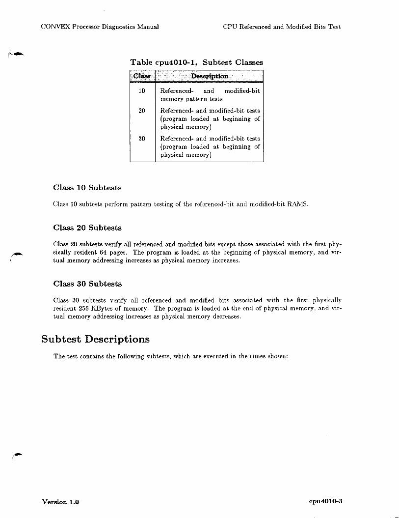
CONVEX Processor Diagnostics Manual CPU Referenced and Modified Bits Test
Table cpu4010-1, Subtest Classes
Glass ... ·.··
r .. · .. <\ Jleseription
10 Referenced- and modified-bit memory pattern tests
20 Referenced- and modified-bit tests {program loaded at beginning of physical memory)
30 Referenced- and modified-bit tests (program loaded at beginning of physical memory)
Class 10 Subtests
Class 10 subtests perform pattern testing of the referenced-bit and modified-bit RAMS.
Class 20 Subtests
Class 20 subtests verify all referenced and modified bits except those associated with the first physically resident 64 pages. The program is loaded at the beginning of physical memory, and virtual memory addressing increases as physical memory increases.
Class 30 Subtests
Class 30 subtests verify all referenced and modified bits associated with the first physically resident 256 KBytes of memory. The program is loaded at the end of physical memory, and virtual memory addressing increases as physical memory decreases.
Subtest Descriptions
The test contains the following subtests, which are executed in the times shown:
Version 1.0 cpu4010-3

CPU Referenced and Modified Bits Test CONVEX Processor Diagnostics Manual
Table cpu4010-2, Subtest Execution Times
10 20 30 40
110 120 130
210 220
10 10 10 10
20 20 20
30 30
Referenced-bits pattern test begin Referenced-bits pattern test end Modified-bits pattern test begin Modified-bits pattern test end
Load test Store test Execute test
Load test Store test
Referenced-Bits Pattern Tests
(Pun:$$)
:10 :10 :10 :10
:30/MB :30/MB :30/MB
:30 :30
Each subtest performs a walking-ones test, an address-uniqueness test, and a pattern/pattern complement test on memory. Subtest 10 perfor est on referenced-bit memory, with the program loaded at the beginning of ysical memor Subtest 20 performs each test on referenced-bit memory with the program loa e at an offset of OxlOOOOO from the beginning of physical memory.
The portions of the referenced and modified bits that correspond to the program and its page table locations in main memory cannot be tested. Subtest 10 does not test a byte of the referenced and modified bits corresponding to the beginning of physical memory. However, subtest 20 does test this byte when the program is loaded at physical location OxlOOOOO.
Modified-Bits Pattern Tests
Each subtest performs a walking-ones test, an address-uniqueness test, and a pattern/pattern complement test on memory. Subtest 30 performs each test on modified-bit memory with the program loaded at the beginning of physical memory. Subtest 40 performs each test on modified-bit memory with the program loaded at an offset of OxlOOOOO from the beginning of physical memory.
The portions of the referenced and modified bits that correspond to the program and its page table locations in main memory cannot be tested. During subtest 30, a byte of the referenced and modified bits corresponding to the beginning of physical memory is not tested. This byte is tested during subtest 40 when the program is loaded at physical location OxlOOOOO.
Load Tests
Subtests 110 and 210 verify the referenced and modified bits by loading data from a memory page and checking that the corresponding referenced bit had been set. They also check that all modified bits have not been set, and that all other referenced bits have not been set.
cpu4010-4 Version 1.0
~ !

~ I
CONVEX Processor Diagnostics Manual CPU Referenced and Modified Bits Test
Store Tests
Subtests 120 and 220 verify the referenced and modified bits by storing data to a memory page and checking that the corresponding referenced and modified bits have been set. They also check that all other referenced and modified bits have not been set.
Execute Tests
Subtest 130 verifies the functionality of the referenced bit by executing code from a memory page and checking that the corresponding referenced bit has been set. It also checks that all modified bits have not been set, and that all other referenced bits have not been set.
Error Messages
For class 1 subtests, an error message displays specifying which part of the test failed (data equals address, pattern/pattern complement, etc.), followed by the address and the expected and actual data patterns. For example:
Test failed during Data Equals Address Test Address: 001000000 Exp. Data: 01 Act Data: 00
For all other classes, the type of test failure (0-10) displays, followed by the specific test that failed. In addition, the address, expected data, and actual data display. If register scan on error is enabled, then a register dump follows the error message.
The type of failure messages are:
Failure Type: 0
Failed referenced bit initialization at 1/0 address: 00000000 Expected byte: DO, Actual byte: 00
Failure Type: 1
Failed Modified Bit initialization at 1/0 address: 00000000 Expected byte: 00, Actual byte: 00
Failure Type: 2 or 4
Failed Untouched Referenced Bit check at 1/0 address: 00000000 Expected byte: 00, Actual byte: 00 Touched Block : O, Touched Page: 000
Failure Type: 3 or 5
Failed Untouched Modified Bit check at 1/0 address: 00000000 Expected byte: 00, Actual byte: 00 Touched Block: O, Touched Page: ODO
Version 1.0 cpu4010-5

CPU Referenced and Modified Bits Test CONVEX Processor Diagnostics Manual
Failure Type: 6
· Failed Touched Modified Bit check at 1/0 address: 00000000 Expected byte: 00, Actual byte: 00 Touched Block : O, Touched Page: 000
Failure Type: 7 or 8
Failed Touched Referenced Bit check at 1/0 address: 00000000 Expected byte: 00, Actual byte: 00 Touched Block: O, Touched Page: 000
Failure Type: 9
Failed Nonresident Block 0 Referenced Bit check at 1/0 address: 00000000 Expected byte: 00, Actual byte: 00
Failure Type: 10
Failed Nonresident Block 0 Modified Bit check at 1/0 address: 00000000 Expected byte: 00, Actual byte: 00
cpu4010-6 Version 1.0

cpu4030
Manufacturing Building Block Tests
Introduction
The Manufacturing Building Block Test ( cpu4030) is the most basic of the CPU functional tests. Cpu4030 begins verification of the CPU by executing a variety of basic instructions out of the instruction cache (icache). This limits the hardware initially tested to the ATU, ASU, and IPU. Once these boards have been proven functional, operations involving memory accesses are tested. First, operand fetches from memory are performed, and later, instruction fetches from memory are tested. These operations are executed with various combinations of caches enabled.
In order for this test to run, the Service Processor Unit (SPU), the memory subsystem, and the following portions of the CPU must be operational: icache, major busses, system registers, and parity.
Test Invocation
To invoke cpu4030, use the following procedure:
Figure cpu4030-1, Test Invocation
(spu)> cd /mnt/test (spu)> 1n1 tall (spu)> dshell
test cpu4030 [-c [class number (s)]] [-s [subtest number (s)]] [ +> filename]
where the arguments enclosed by [ ] are optional. Entering only the testname ( cpu4030) executes all cpu4030 tests sequentially. You can execute a specific class(es) of subtest(s) or one or more individual subtests by using the -c or -s options, respectively. (For more information on using these options refer to the "Dshell and Scan Overview" chapter.) The [ +> filename] option ensures that all test results are placed in filename.
During the first phase of testing, you are presented with a test menu (Figure cpu4030-1) that allows you to choose various test execution options. Possible options are displayed inside brackets [ ] , separated by slashes. You can select default options, which are displayed inside parentheses ( ), with a carriage return.
Version 1.0 cpu4030-1

CPU Manufacturing Building Block Test CONVEX Processor Diagnostics Manual
When the test begins execution, the following prompt displays:
Use default parameters [y /n] (y)
If you respond with y or <CR>, no additional test parameter queries display; the testing begins. However, if you give a negative response, additional queries display allowing you to modify the default selections.
Figure cpu4030-2, Test Parameter Menu
[] Encloses allowed ranges or values 0 Encloses default
Moves to previous prompt or aborts input :nn Moves to prompt nn; O aborts input
Moves to first unsatisfied prompt
Use default parameters? [y/n] Verify main memory load? [y/n] Enable icache? [y/n] Enable pcache? [y/n] Enable lcache? [y/n] Enable virtual addressing? [y/n] Enable continuous looping? [y/n] Invoke interactive scan? [y/n] Enable debug options? [y/n] Input OK, or to question :nn ? [OK]
(y)
(y) (y) (y)
(n)
(OK)
->n (n) -> -> -> (y) (n) (n)
->y ->
->
-> -> ->
Responding n to the first parameter query displays the following queries:
Verify main memory load?
An affirmative answer to this query results in verification of all main memory object and data file loads from the SPU. This ensures that failures are not caused by an incorrect main memory image.
Enable icache?
This query allows you to disable or enable the instruction cache.
Enable pcache?
This query allows you to disable or enable the physical cache.
Enable lcache?
This query allows you to disable or enable the logical cache.
cpu4030-2 Version 1.0

CONVEX Processor Diagnostics Manual CPU Manufacturing Building Block Test
Enable physical or virtual addressing?
Selecting physical addressing causes all address translation functions of the hardware to be disabled, and the test to be run out of block 0 in main memory. If block 0 is not present in memory, an error indication is displayed. If you select virtual addressing, then all address translation functions of the hardware are enabled.
Enable continuous looping?
Use this option whenever a specific set of instructions must be tested continuously.
Invoke interactive scan?
An affirmative response invokes the interactive scan package after ring initialization has occurred and prior to starting the CPU's clocks. Thus, since the test actually invokes the interactive scan utility after initialization of the cpu, you can perform individual checks instead of the ones normally performed by the test.
(NOTE) Only experienced hardware engineers with intimate knowledge of the CPU and interactive scan package should use this option.
Enable debug options?
Enabling the debug option allows you to select the scan operations to display during test execution. When you enable the debug option, the following prompts appear:
Figure cpu4030-3, Selecting the Scan Operations
Dump global parms? [y/n] (n) -> Dump mem start? [y/n] (n) -> Dump subtest table? [y/n] (n) -> Dump MM-->IC data? [y/n] (n) -> Dump v mem results? [y/n] (n) -> Dump routine inputs? [y/n] (n) -> Dump test flow data? [y/n] (n) ->
These debug options allow an experienced engineer to utilize intermediate results and test parameter information to analyze a test sequence step-by-step. The following paragraphs describe the debug options.
Dump global parms?
An affirmative response displays parameters used by jpstart.
Version 1.0 cpu4030-3
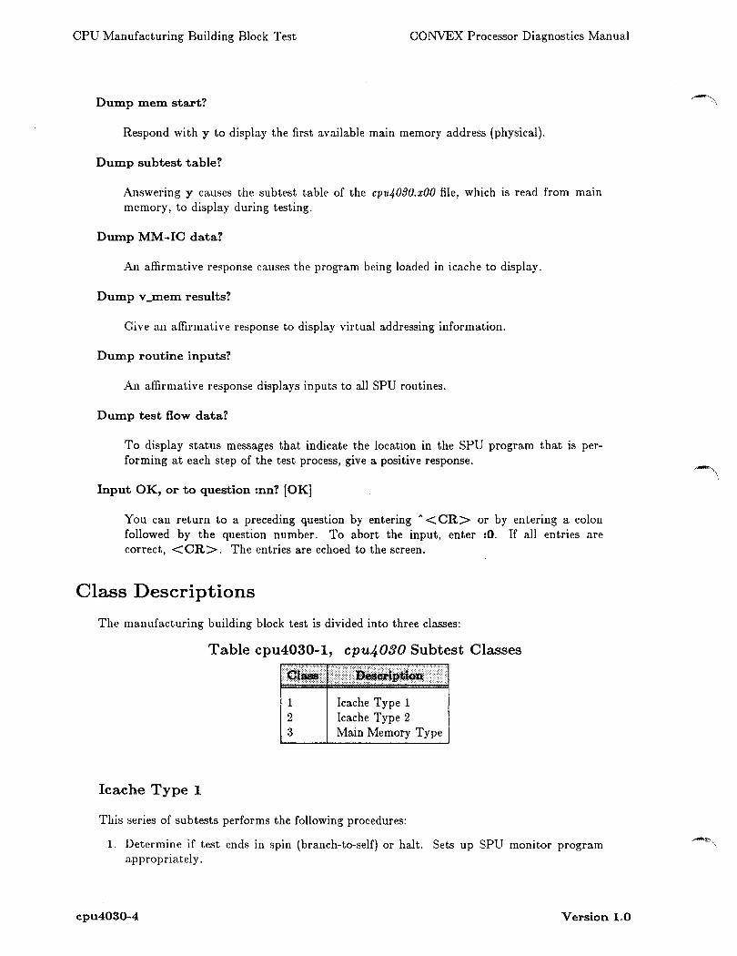
CPU Manufacturing Building Block Test CONVEX Processor Diagnostics Manual
Dump mem start?
Respond with y to display the first available main memory address (physical).
Dump subtest table?
Answering y causes the subtest table of the cpu4030.x00 file, which is read from main memory, to display during testing.
Dump MM .. IC data?
An affirmative response causes the program being loaded in icache to display.
Dump v _mem results?
Give an affirmative response to display virtual addressing information.
Dump routine inputs?
An affirmative response displays inputs to all SPU routines.
Dump test flow data?
To display status messages that indicate the location in the SPU program that is performing at each step of the test process, give a positive response.
Input OK, or to question :nn? [OK]
You can return to a preceding question by entering "<CR> or by entering a colon followed by the question number. To abort the input, enter :0. If all entries are correct, <CR>. The entries are echoed to the screen.
Class Descriptions
The manufacturing building block test is divided into three classes:
Table cpu4030-1, cpu4oso Subtest Classes
1 lcache Type 1 2 lcache Type 2 3 Main Memory Type
lcache Type 1
This series of subtests performs the following procedures:
1. Determine if test ends in spin (branch-to-self) or halt. Sets up SPU monitor program appropriately.
cpu4030-4 Version 1.0

CONVEX Processor Diagnostics Manual CPU Manufacturing Building Block Test
r I 2. Load icache with instruction pattern to be executed.
3. Start CPU with parameters specifying lcache execution.
4. Monitor CPU for timeout or halt condition.
5. Read/Verify CPU registers via scan for proper results.
6. Read/dump CPU registers on fail noting expected results.
7. Dump pattern start address on fail.
These icache-executed tests rely on the SPU to perform the pass/fail analysis.
Icache Type 2
This series of subtests performs the following procedure:
1. Load icache with instruct.ion pattern to be executed.
2. Start CPU with paramet.ers specifying icache execution.
3. Monitor CPU for timeout or halt condition.
4. Read/Verify predefined CPU register via scan for pass/fail.
5. Read/dump CPU registers on fail.
6. Dump pattern start address on fail.
1~, These icache-executed tests perform the pass/fail analysis using CPU instructions.
Main Memory Type
This series of subtests performs the following procedure:
1. Load main memory with instruction pattern.
2. Start CPU with parameters specifying main memory execution.
3. Monitor CPU for timeout or halt condition.
4. Read/Verify predefined CPU register via scan for pass/fail.
5. Read/dump CPU registers on fail.
6. Dump pattern start address on fail.
These subtests are executed from main memory using instruction fetches.
Subtest Descriptions
The Manufacturing Building Block Test is divided into subtests that verify a subset of the instruction of the CONVEX Archi'tecture Reference. It tests only the CPU hardware in a hierarchical manner; it is not intended to test the entire Cl or C120 instruction set. When a failure is detected, a halt instruction is executed.
r The test contains the following subtests, which execute in the times shown:
Version 1.0 cpu4030-5

CPU Manufacturing Building Block Test CONVEX Processor Diagnostics Manual
Table cpu4030-2, cpu4030 Subtest Execution Times
5 1 Spin :06 IO 1 Halt :03 15 1 Load Immediate :03 20 1 Move :03 25 1 Move PC :03 26 1 Move PSW :03 30 1 Logical: and :03 31 1 Logical: or :03 32 1 Logical: xor :03 33 1 Logical: not :03 35 1 Add :03 36 1 Sub :03 37 1 Neg :03 40 1 Branch :03 45 1 Compare: Addr register to register: halfword :03 46 1 Compare: Addr register to register: word :03 47 1 Compare: Addr register to immediate: halfword :03 48 1 Compare: Addr register to immediate: word :03 49 1 Compare: Scalar register to register: byte :03 50 1 Compare: Scalar register to register: halfword :03 51 l Compare: Scalar register to register: word :03 52 1 Compare: Scalar register to register: longword :03 53 1 Compare: Scalar register to immediate: halfword :03 54 1 Compare: Scalar register to immediate: word :03 60 1 Shift reg-reg :03 61 1 Shift immediate :03 65 1 Jump :03
cpu4030-6 Version 1.0

CONVEX Processor Diagnostics Manual CPU Manufacturing Building Block Test
~ Table cpu4030-2, cpuJ,030 Subtest Execution Times I
continued
Time. (mm:ss)
100 2 Load addr register byte (Icache) :03 101 2 Load addr register halfword (le ache) :03 102 2 Load addr register word (le ache) :03 103 2 Load scalar register byte (Icache) :03 104 2 Load scalar register half word (Icache) :03 105 2 Load scalar register word (Icache) :03 106 2 Load scaiar register longword (Icache) :03 107 2 Load addr register halfword unaligned (Icache) :0:3 108 2 Load addr register word unaligned (Icache) :0:3 109 2 Load scalar register halfword unaligned (Icache) :03 110 2 Load scalar register word unaligned (le ache) :03 111 2 Load scalar register longword unaligned (le ache) :0:3 120 2 Store addr register byte (Icache) :0:3 121 2 Store addr register halfword (Icache) :0:3 122 2 Store addr register word (I cache) :03 123 2 Store scalar register byte (Icache) :03 124 2 Store scalar register half word (Icache) :03 125 2 Store scalar register word (le ache) :03 126 2 Store scalar register longword (le ache) :03 127 2 Store addr register halfword unaligned (le ache) :03 128 2 Store addr register word unaligned (le ache) :03 129 2 Store scalar register halfword unaligned (le ache) :03 130 2 Store scalar register word unaligned (le ache) :03 131 2 Store scalar register longword unaligned (Icache) :03 132 2 Indirect load, store, jump (Icache) :03 140 2 Callq/Rtnq (le ache) :03 141 2 Callq/Rtnq word aligned (le ache) :03 142 2 Call/Return (Icache) :03 143 2 Call/Return word aligned (Icache) :03 144 2 Calls/Return (Icache) :03 145 2 Calls/Return word aligned (Icache) :03
Version 1.0 cpu4030-7

CPU Manufacturing Building Block Test CONVEX Processor Diagnostics Manual
Table cpu4030-2, cpu4030 Subtest Execution Times continued
~ini~ (pini:ss)
150 3 Fetch (MM) :03 200 3 Load addr register byte (MM) :03 201 3 Load addr register halfword (MM) :03 202 3 Load addr register word (MM) :03 203 3 Load scalar register byte (MM) :0;3 204 3 Load scalar register halfword (MM) :03 205 3 Load scalar register word (MM) :0:3 206 3 Load scalar register longword (MM) :03 207 3 Load addr register half word unaligned (MM) :03 208 3 Load addr register word unaligned (MM) :0:3 209 3 Load scalar register halfword unaligned (MM) :0:3 210 3 Load scalar register word unaligned (MM) :0:3 211 3 Load scalar register longword unaligned (MM) :0:3 220 3 Store addr register byte (MM) :03 221 3 Store addr register halfword (MM) :0:3 222 3 Store addr register word (MM) :0:3 223 3 Store scalar register byte (MM) :03 224 3 Store scalar register halfword (MM) :03 225 3 Store scalar register word (MM) :03 226 3 Store scalar register longword (MM) :03 227 3 Store addr register halfword unaligned (MM) :03 228 3 Store addr register word unaligned (MM) :03 229 3 Store scalar register halfword unaligned (MM) :03 230 3 Store scalar register word unaligned (MM) :03 231 3 Store scalar register longword unaligned (MM) :03 232 3 Indirect load, store, jump (MM) :03 240 3 Callq/Rtnq (MM) :03 241 3 Callq/Rtnq word aligned (MM) :03 242 3 Call/Return (MM) :03 243 3 Call/Return word aligned (MM) :03 244 3 Calls/Return (MM) :03 245 3 Calls/Return word aligned (MM) :03
The CPU will attempt to execute the program (regardless of initial starting source) and report the results. Except during the spin subtest, the CPU instruction sequence executes a halt instruction to signal the SPU when the test is finished. The spin subtest performs a branch-to-self, which causes the SPU to time out. Because the SPU expects the timeout on this subtest, it continues to the verification sequence.
cpu4030-8 Version 1.0
~

cpu4040
Vector Concurrency Tests
Introduction
The Vector Concurrency test ( cpu4040} verifies the vector processor unit operation under all possible combinations of the instructions from the three groups listed in Table cpu4040-l. Each group of instructions corresponds to one of the three controllers on the vector process unit: load/store, add/logical, and multiply/ divide.
Cpu4040 assures that instructions from each set tested can execute concurrently and return the expected results. Because cpu4040 checks test results against self-generated expected values, the scalar port.ion of the CPU is assumed to be operational. Also, enough of the vector unit must be operational t.o perform scalar floating-point arithmetic and scalar-register to vector-register moves. This hardware can be verified by running cpu4000 subtests 317, 365, 405, 415, 465, and 638.
Table cpu4040-1, Vector Instruction Groups
0 mov sO,sl,vO add.s s3,s4 prod.w vO 1 mov vO,sO,sl add.cl s4,s3 prod.l vl 2 mov al,vl sum.w v4 mul.s s5,s6 3 mov sl,s2,vm add.w v0,vl,v2 div.w a3,a4 4 mov sl,vm,s2 add.w v0,vl,v4 div.l s6,s7 5 merg.t vO,sl,vl add.w v0,v4,v4 mul.w v0,vl,v4 6 merg.t v0,sl,v4 add.w vl,v5,v6 mul.w v0,vl,v2 7 mask.t v0,vl,v2 add.w v2,v3,v7 mul.w v0,v4,v4 8 mask.t v0,vl,v4 add.w v2,v2,v6 mul.w vl,v5,v2 9 mask.t v0,v0,v4 sum.l v5 mul.w vl,v6,v2 10 mask.t v0,v4,v3 not vl,v5 mul.w v3,v3,v7 11 mask.t v2,v0,v4 not v0,v4 mul.d v0,vl,v4 12 mask.t v0,v4,v4 shf s4,v0 mul.d v0,vl,v2 13 mask.t v5,sl,v7 plc.t vO,vl mul.d v0,v4,v4 14 mask.t v2,sl,v6 plc.t v2,v6 mul.d v3,v7,vl 15 cprs.t vO,vl eq.w s4,v0 mul.d vl,v6,v2 16 cprs.t v3,v7 lt.l s4,v3 mul.d vl,vl,v5 17 ldvi.w v5,v6 lt.w s4,v6 div.w v0,vl,v4 18 ldvi.w v3,v7 eq.l s4,v4 div.w v0,vl,v2 19 ldvi.l vO,vl plc.t vm,s4 div.w v0,v4,v4 20 ldvi.l v0,v4 add.l v0,vl,v2 div .w v2,v6,v3 21 stvi.w sO,vO add.l v0,vl,v4 div.w v3,v7,v0 22 merg.t v0,vl,v2 add.l v0,v4,v4 div.w vl,vl,v5 23 merg.t v0,vl,v4 add.l v3,v7,v5 div.l v0,vl,v4 24 merg.t vl,v5,v7 add.l v7,v5,vl div.l v0,vl,v2
Version 1.0 cpu4040-1

CPU Vector concurrency Tests CONVEX Processor Diagnostics Manual
Table cpu4040-1, Vector Instruction Groups continued
25 merg.t v3,v2,v6 add.I v2,v2,v6 div.I v0,v4,v4 26 stvi.l sl, vO eq.w v6,v7 div.I vl,v5,v2 27 stvi.w vO,vl eq.w v3,v7 div.I v2,v6,v7 28 stvi.w vl,v5 eq.l v5,v6 div.I v3,v3,v7 29 stvi.l v2,v3 eq.l vl,v5 mul.d s6,s7 30 stvi.l v3,v7 max.w vO div.w s6,s7 31 ld.w (a2),v0 max.I v7 mul.w a3,a4 32 Id.I (a2),v0 eq.s s3,s4 mul.w v0,s5,vl 33 st.w v0,(a2) eq.d s3,s4 mul.w v0,s5,v4 34 st.I v6,(a2) add.w v0,s3,vl mul.d v0,s5,v5 35 add.w v2,s3,v6 mul.d v2,s5,v6 36 add.I v6,s3,v7 div.w v0,s5,vl 37 add.I vl,s3,v5 div.w v0,s5,v4 38 div.I v0,s5,v5 39 div.I v2,s5,v6
Test Invocation
To invoke the cpu4040 test, use the following procedure:
Figure cpu4040-1, Test Invocation
(spu)> cd /mnt/test (spu)> ini tall (spu)> dshell
test cpu4040 [-c [class number (s)]] [-s [subtest number Cs)]] [ +> filename]
where the arguments enclosed by [ ] are optional. Entering only the testname (cpu4040) executes all cpu4040 tests sequentially. You can execute a specific class(es) of subtest(s) or one or more individual subtests by using the -c or -s options, respectively. (For more information on using these options refer to the "Oshell and Scan Overview" chapter.) The [ +> filename] option ensures that all test results are placed in filename.
When you invoke the cpu4040 test, a test menu displays. This menu allows you to choose various test execution options, which appear between brackets [ ] , separated by slashes. You can select default options, which are displayed between parentheses ( ), with a carriage return.
When the test begins execution, the following prompt displays:
cpu4040-2 Version 1.0

CONVEX Processor Diagnostics Manual CPU Vector concurrency Tests
Run default switches [y/n] (y)
If you respond with y or <CR>, no additional test parameter queries display; the testing begins. However, if you give a negative response, the following queries display allowing you to modify the default selections.
Figure cpu4040-2, Test Parameter Menu
[] Encloses allowed ranges or values () Encloses default
Moves to previous prompt or aborts input :nn Moves to prompt nn; O aborts input
Moves to first unsatisfied prompt
Run default switches? [y/n] SW test mode? [y/n] Debugger on? [y/n] Forced fail enable? [y/n] Main memory load verification? [y/n] Force display of all regs on error? [y/n] Display update mode: [n/f] Test display mode: [s/l] Lcache enabled? [y/n] Pcache enabled? [y/n] Virtual memory enabled? [y/n] Continuous faulting enabled? [y/n] Current group indexes:
Group (0) :O Group (1) :O Group (2) :O
Continuous loop? [y/n]
(y)
Cn) Cy) Cf)
Cy) Cy) (y) (n)
Cn)
->n (n)
Cy) Cn) -> -> -> Cs) -> -> -> ->
->
-> -> ->
->
-> -> ->
The following prompts display one line at a time when you answer the initial test parameter query with n, as illustrated in Figure cpu4040-2.
SW test mode?
Answering yes to this prompt disables permutation of the selected instructions and allows the test to execute six times faster. This mode is only enabled when performing verification of the program.
Debugger on?
If you answer y, the program enters a debug mode whenever a test fails. (See "Debugger Description" in this section for more information.)
Forced fail enable?
If you enable forced failed, the CPU acts as if a fail occurs at the end of each instruction group tested. This is normally used in conjunction with the debugger when debugging instruction sequences.
Version 1.0 cpu4040-3

CPU Vector concurrency Tests CONVEX Processor Diagnostics Manual
Main memory load verification?
An affirmative answer to this query results in verification of all main memory object and data file loads from the SPU. This allows you to be sure that failures a.re not caused by an incorrect main memory image.
Force display of all regs on error?
Answering y to this prompt displays failing vector registers automatically on any failing instruction sequence. Answering n causes the test to stop at each failing vector register and display the following prompt:
Display initial? expected?
actual?
where initial displays the initialized condition of the register(s), e;1;pected displays the expected value of the register(s), and actual displays the a.dual value of the regist.er(s) at the failure.
Display update mode
Answering n (normal) to this prompt forces the CPU to delay further testing while instruction information is sent to the screen. The fast default (f) allows the CPU to continue processing at the same time information is going to the screen.
Test display mode
If you select short mode (s), only the numbers are displayed. For example:
Groups: 0 1 1 Perm: B3
This display is written over itself on a CRT or scrolled on a hard copy terminal.
If you answer I (long) to this prompt, the names as well as the corresponding index numbers of the three instructions being tested appear on the screen. The long display is useful for monitoring the progression of the test through the various instructions. For example:
Groups: 0 1 1 Perm: B3
Instructions: Badd. d s4. s3 mov sO.sl.vO prod.l v1
This display is scrolled on either a CRT or a hard copy terminal.
Lcache enabled?
This query allows you to enable or disable the logical cache.
cpu4040-4 Version 1.0
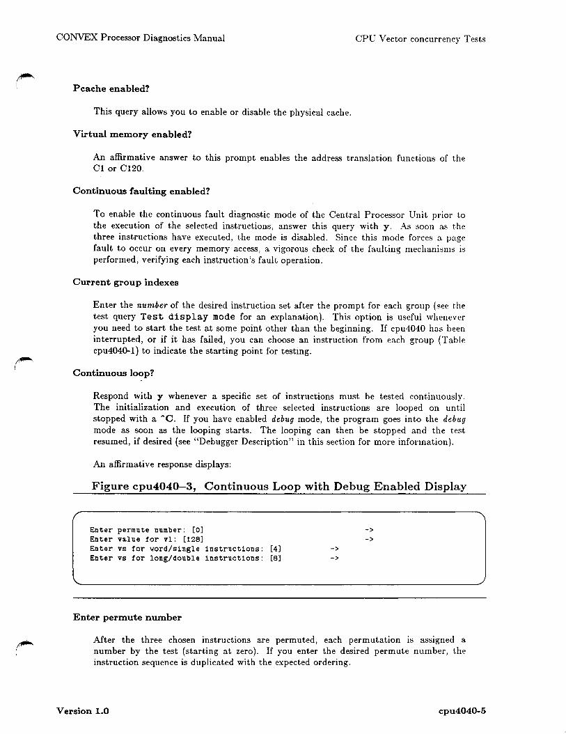
CONVEX Processor Diagnostics Manual CPU Vector concurrency Tests
Pcache enabled?
This query allows you to enable or disable the physical cache.
Virtual memory enabled?
An affirmative answer to this prompt enables the address translation functions of the Cl or C120.
Continuous faulting enabled?
To enable the continuous fault diagnostic mode of the Central Processor Unit prior to the execution of the selected instructions, answer this query with y. As soon as the three instructions have executed, the mode is disabled. Since this mode forces a page fault to occur on every memory access, a vigorous check of the faulting mechanisms is performed, verifying each instruction's fault operation.
Current group indexes
Enter the number of the desired instruction set after the prompt for each group (see t.he test query Test display mode for an explanation). This option is useful whenever you need to start the test at some point other than the beginning. If cpu4040 has been interrupted, or if it has failed, you can choose an instruction from each group (Table cpu4040-1) to indicate the starting point for testing.
Continuous loop?
Respond with y whenever a specific set of instructions must be tested continuously. The initialization and execution of three selected instructions are looped on until stopped with a "C. If you have enabled debug mode, the program goes into the debug mode as soon as the looping starts. The looping can then be stopped and the test resumed, if desired (see "Debugger Description" in this section for more information).
An affirmative response displays:
Figure cpu4040-3, Continuous Loop with Debug Enabled Display
Enter permute number: [O] Enter value for vl: [128] Enter vs for word/single instructions: [4] Enter vs for long/double instructions: [8]
Enter permute number
-> ->
-> ->
After the three chosen instructions are permuted, each permutation is assigned a number by the test (starting at zero). If you enter the desired permute number, the instruction sequence is duplicated with the expected ordering.
Version 1.0 cpu4040-5

CPU Vector concurrency Tests CONVEX Processor Diagnostics Manual
Enter value for vi
This is the value that will be loaded into the vi register prior to execution.
Enter vs for word/single instructions
This is the value that will be loaded into the vs register prior to execution if the instruction sequence uses only word and single operands.
Enter vs for long/ double instructions
This is the value that will be loaded into the vs register prior to execution if the instruction sequence uses any double or long operands.
If you do not select continuous loop, the following prompts appear on the screen:
Figure cpu4040-4, Continuous Loop Not Selected
Number of vl values to check: [3] Current set of vl values:
Vl-0:[1] Vl-1: [64] Vl-2: [128]
Number of vs values to check: [2] Current set of vs for words and singles:
Vs-0: [4] Vs-1: [33]
Current set of vs for longs and doubles: Vs-0: [8] Vs-1: [33]
Number of vi values to check
->
-> -> ->
->
-> ->
-> ->
Cpu4040 is executed with various values of vi, which are stored in an array. You must specify the length of this array.
Current set of vi values
The values of vi are displayed one at a time. You can change the value of any vi element after it appears.
Number of vs values to check
Cpu4040 is executed with various values of vs, which are stored in an array. You must specify the length of this array.
cpu4040-6 Version 1.0
~.

~ I
CONVEX Processor Diagnostics Manual CPU Vector concurrency Tests
Current set of vs for words and singles
This option displays the values of vs that are used when an instruction sequence contains only single and word operands. You can change the value of any vs element after it appears.
Current set of vs for longs and doubles
This option displays the values of vs that are used when an instruction sequence contains any double or long operands. You can change the value of any vs element after it appears.
Debugger Description
Cpu4040 provides an internal debugger that you can use as a system troubleshoot.ing aid. The debugger allows you to display the contents of registers and memory that are not normally displayed when a test fails.
Responding with y to the test parameter query:
Debugger on [y.n]
automatically invokes the cpu4040 debugger whenever a subtest fails. When invoked, the debugger displays a debug> prompt.
You can use any of the following debugger commands:
Table cpu4040-2, Debugger Commands
c Compares registers d Displays memory f Displays failing instructions l Starts looping on failed instructions q Quits (exits) debug mode and continues testing r Displays registers s Stops looping on failed instructions ? Displays the help file
You can use the following register data type and register mnemonic operands with the debugger commands:
Version 1.0 cpu4040-7
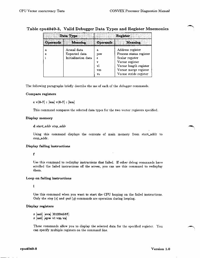
CPU Vector concurrency Tests CONVEX Processor Diagnostics Manual
Table cpu4040-3, Valid Debugger Data Types and Register Mnemonics
a Actual data a Address register e Expected data psw Process status register
Initialization data s Scalar register v Vector register vl Vector length register vm Vector merge register VS Vector stride register
The following paragraphs briefly describe the use of each of the deb11gger commands.
Compare registers
c v[0-7] : [iea] v[0-7] : [iea]
This command compares the selected data types for the two vector registers specified.
Display memory
d start_addr stop_addr
Using this command displays the contents of main memory from start_addr to stop_addr.
Display failing instructions
f
Use this command to redisplay instructions that failed. If other debug commands have scrolled the failed instructions off the screen, you can use this command to redisplay them.
Loop on failing instructions
Use this command when you want to start the CPU looping on the failed instructions. Only the stop ( s) and quit ( q) commands are operation during looping.
Display registers
r [aei] [sva] [01234567] r [aei] [spw vi vm vs]
These commands allow you to display the' selected data for the specified register. You can specify multiple registers on the command line.
cpu4040-8 Version 1.0
CONVEX Processor Diagnostics Manual CPU Vector concurrency Tests
Stop looping
s
Using this command terminates looping initiated via the I command and returns to the debugger prompt.
Class Descriptions
Class 1 contains the subtests for verifying vector processor unit operation.
Table cpu4040-4, Class 1 Subtests :· .. :· ·::· '·: .
. /.•.··••·.· J'eserlption .. • + ······ . . . ..
1 Concurrent vector instruction test
Subtest Descriptions
Test Method
An instruction is chosen from each column based on the current index numbers. This number is determined by the test instruction's location in the test table (see Table cpu4040-l). The selected instructions are permuted, and the registers are checked to see whether the instructions chain (the destination register of one instruction is used as the source register of another). Depending on the subtest being run, the instructions are either tested or discarded (see individual subtest descriptions in this section).
Next, the registers in each of the register spaces are initialized, and the emulation routines are called to emulate the instructions under test. The registers are loaded with the initialized values, and the instructions are executed. The registers are then saved, and the compare routine compares the emulation and execution results. If the test passes, it continues to the next permutation, but if it fails, the CPU halts.
When all six permutations have been checked, the table indexes are changed, and the next group of three instructions are tested. After all instructions have been checked, vi is changed, and all instructions are checked again. After all values of vi have been tested with all combinations of instructions, the value of vs is changed. Cpu4040 tests all values of vi, all values of vs, and all possible instruction combinations before finishing.
Although all registers that are operands of the instructions being executed are initialized by a random number before use, these numbers are generated from a seed that is set at the beginning of each test sequence. This means that each permutation of instructions will have the registers initialized to different values. However, when an instruction sequence is looped on, the registers are always looped from the same initialized value. Of course, registers that contain the indexes in a vector of indexes instruction are not randomly initialized, and registers that contain the address for a vector load or store operation are not randomly initialized. In addition, vector registers used in prod.I, prod.w, and mul.w vi,vj,vk instructions have the input values limited to prevent overflow. These registers also are never initialized to zero.
Version 1.0 cpu4040-9
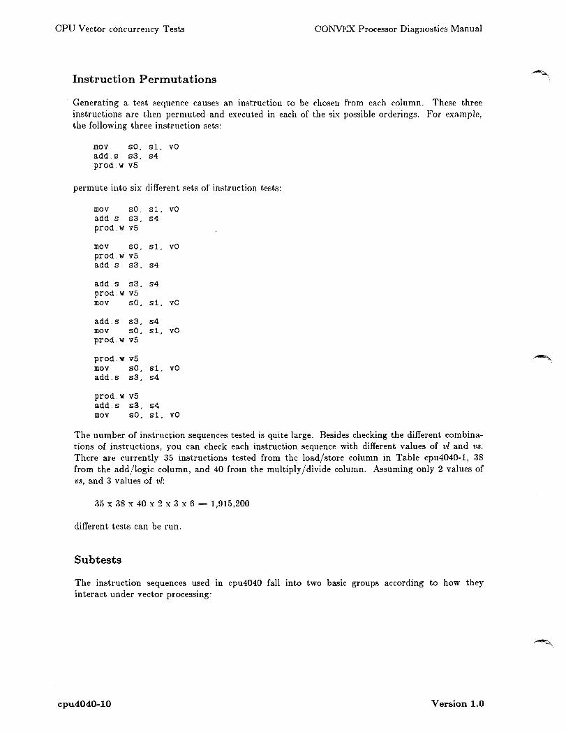
CPU Vector concurrency Tests CONVEX Processor Diagnostics Manual
Instruction Permutations
Generating a test sequence causes an instruction to be chosen from each column. These three instructions are then permuted and executed in each or the six possible orderings. For example, the following three instruction sets:
mov so. s1. vo a.dd.s s3. s4 prod. w v5
permute into six different sets or instruction tests:
mov so. s1. VO a.dd.s s3. s4 prod.w v5
mov so. s1. VO prod.w v5 a.dd.s s3. s4
a.dd.s s3. s4 prod.w v5 mov so. s1. VO
a.dd.s s3. s4 mov so. s1. VO prod.w v5
prod.w v5 mov so. s1. VO a.dd.s s3. s4
prod.w v5 a.dd.s s3. s4 mov so. s1. VO
The number or instruction sequences tested is quite large. Besides checking the different combinations of instructions, you can check each instruction sequence with different values of vi and vs. There are currently 35 instructions tested from the load/store column in Table cpu4040-1, 38 from the add/logic column, and 40 from the multiply/divide column. Assuming only 2 values of vs, and 3 values of vi:
35 x 38 x 40 x 2 x 3 x 6 = 1,915,200
different tests can be run.
Sub tests
The instruction sequences used in cpu4040 fall into two basic groups according to how they interact under vector processing:
cpu4040-10 Version 1.0
~
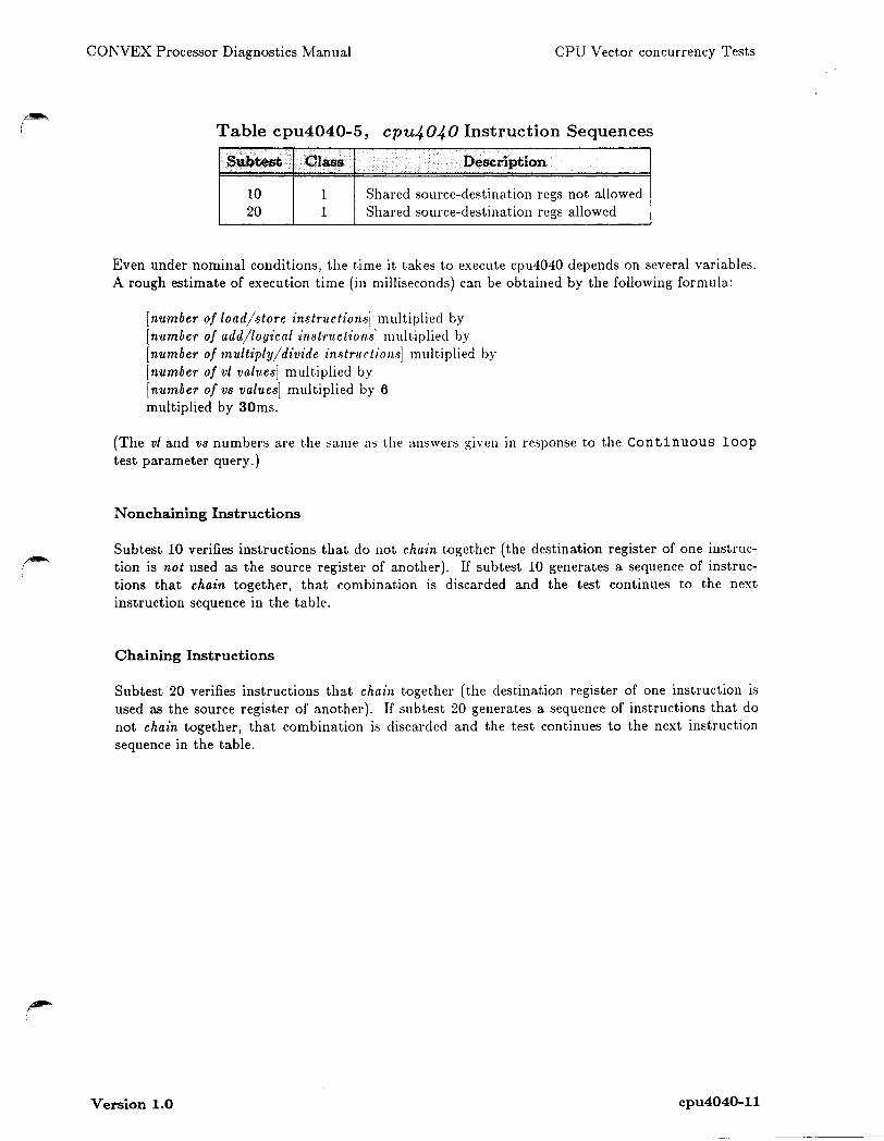
'~ '
~ I
CONVEX Processor Diagnostics Manual CPU Vector concurrency Tests
Table cpu4040-5, cpu4040 Instruction Sequences
Subtest Class Description
10 1 Shared source-destination regs not allowed 20 1 Shared source-destination regs allowed
Even under nominal conditions, the time it takes to execute cpu4040 depends on several variables. A rough estimate of execution time (in milliseconds) can be obtained by the following formula:
[number of load/store instrnction.s] multiplied by [number of add/logical instrnction.s] multiplied by [number of multiply/divide instruction.s] multiplied by [number of vi values] multiplied by [number of vs values] multiplied by 6 multiplied by 30ms.
(The vi and vs numbers are the same as the answers given in response to the Continuous loop test parameter query.)
Nonchaining Instructions
Subtest 10 verifies instructions that do not chain together (the destination register of one instruction is not used as the source register of another). If subtest 10 generates a sequence of instructions that chain together, that combination is discarded and the test continues to the next instruction sequence in the table.
Chaining Instructions
Subtest 20 verifies instructions that chain together (the destination register of one instruction is used as the source register of another). If subtest 20 generates a sequence of instructions that do not chain together, that combination is discarded and the test continues to the next instruction sequence in the table.
Version 1.0 cpu4040-11

CPU Vector concurrency Tests CONVEX Processor Diagnostics Manual
~ THIS PAGE INTENTIONALLY LEFT BLANK
)
cpu4040-12 Version 1.0
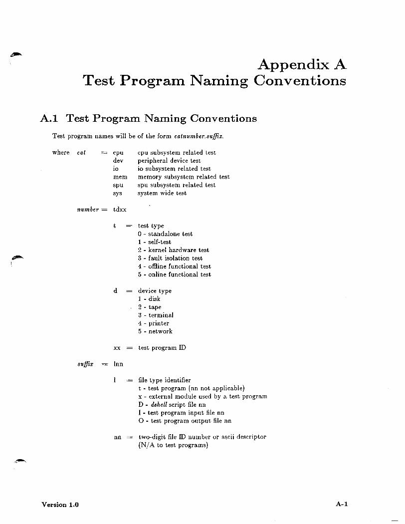
Appendix A Test Program Naming Conventions
A.I Test Program Naming Conventions
Test program names will be of the form catnumber.suffix.
where cat cpu cpu subsystem related test dev peripheral device test io io subsystem related test mem memory subsystem related test spu spu subsystem relat.ed test sys system wide test
number = tdxx
t test type 0 - standalone test 1 - self-test 2 - kernel hardware test 3 - fault isolation test 4 - offtine functional test 5 - online functional test
d device type 1 - disk 2 - tape 3 - terminal 4 - printer 5 - network
xx = test program ID
suffix Inn
Version 1.0
file type identifier t - test program (nn not applicable) x - external module used by a test program D - dshell script file nn I - test program input file nn 0 - test program output file nn
nn two-digit file ID number or ascii descriptor (N /A to test programs)
A-1

Test Program Naming Conventions CONVEX Processor Diagnostics Manual
Examples:
A-2
mem4000.t
mem4000.D mem4000.I mem4000.0
Memory subsystem functional test
Dshell script for default mem.4000.t Input script for default mem.4000.t Output file name for default mem.4000.t
mem4000.D_pbus mem4000.Lpbus mem4000.0_pbus
Dshell script for PBUS only mem.4000.t Input script for PBUS only mem.4000.t Output filename for PBUS only mem.4000.t
Table A-1, Test Program Name Assignments
cpu4000 CPU instruction set test cpu4010 CPU read/modify bits test cpu4030 CPU building block test cpu4040 Vector concurrency test
dev4100 Xylogic 450/451 SMD disk test dev4110 SMD disk formatter /interactive test dev4200 :MBTC/STC 2920, STC 1968 tape unit test dev4300 Systech MTI-1600-A/terminal test dev4400 Systech MLP-2000/line printer test dev4410 Versatec plotter functional test dev4500 Ethernet controller functional test dev4510 Hyperchannel controller functional test dev4600 IKON DR-llW controller test
iolOOO IOP self-test io4000 IOP test io4100 HSP subsystem test
mem4000 Main memory test
spulOOO SPU self-test spu2000 SPU peripheral test spu4000 SPU diagnostic subsystem test spu4100 SPU cartridge tape and file system test
Version 1.0
~.

A Address and scalar unit (ASU) cpu4000-1 Address translation unit (ATU) cpu4000-1 Address-address complement test (MBUS)
mem4000-5 Arbitrary pattern read test spu4100-4 Arbitrary pattern write test spu4100-4 Assembly language instruction test cpu4000-1 ASU (address and scalar unit) cpu4000-1 ATU (address translation unit) cpu4000-1
B Bad block fix subtest spu2000-8 Boot device test spul000-7
c C Programming Language xx Cartridge tape spul000-1 Cartridge tape and file system test spu4100-1 Cartridge tape pattern tests spu4100-3 Cartridge tape seek tests spu4100-3 Cartridge tape/file system arbitrary pattern
write test spu4100-4 Cartridge/file system arbitrary pattern read
test spu4100-4 Cartridge/file system seek test spu4100-4 Cartridge/file system write seek test pattern
test spu4100-4 Class 1 subtests, mem4000 mem4000-4 Class 9-16 subtests cpu4000-12 Class descriptions cpu4010-2 Command scripts, user-created 2-1 Controller error codes spul000-11 CONVEX Archi'tecture Reference xx CONVEX Diagnostic Utilities Manual (Cl,
C120) xx CONVEX Diagnostic Utilities Manual (C130,
C210, C220) xx CONVEX Processor Operation Guide (Cl,
C120, C130, C210, C220} xx CONVEX UNIX Tutorial Papers xx cpu XIX
CPU cache feature tests cpu4000-5, cpu4000-18
CPU instruction boundary conditions tests cpu4000-4, cpu4000-12
CPU instruction set test cpu4000-1, cpu4000-2, cpu4010-1
CPU instruction set test, class 30 cpu4000-19 CPU instruction set test, subtest 1000
cpu4000-19 CPU instruction set tests cpu4000-4 CPU, subsystem tests, prefix identifying XIX
CPU Utility Board. See CPX Cpu4000 (CPU instruction set test)
cpu4000-1 Cpu4000 test parameter menu cpu4000-2 Cpu4010 (referenced and modified bits test)
cpu4010-1 Cpu4030 (manufacturing building block tests)
cpu4030-1
Index
Cpu4030 test parameter menu cpu4030-2 Cpu4040 test parameter menu cpu4040-3 Cpu4040 (vector concurrency tests)
cpu4040-1
D dev xix Diagnostic shell. See dshell Diagnostic test overview 1-1 Diagnostic tests, layout of xix Diagnostics, selecting 2-1 Diagnosti~s, subsystem tests, prefix identifying
XIX
Disable self-test spul000-2 dshell, introduction 2-1 dshell, overview 2-1
E Error codes spu2000-9 Error descriptions spu2000-10 Error messages, selecting 2-1 Exception tests cpu4000-5, cpu4000-18
F Files, test outputs to 2-1 Floating point test cpu4000-19 Format subtest spu2000-8 Functional tests 1-2
I Instruction processor unit (IPU) cpu4000-1 Interrupt tests (PBUS) mem4000-1,
mem4000-5 ZO XIX
I/O, subsystem tests, prefix identifying XIX
!Omega disks, subtests for spu2000 spu2000-6
IPU (instruction processor unit) cpu4000-1
L Load subtests, referenced and modified bits
cpu4010-4
M Main memory address error test mem4000-1,
mem4000-11 Main memory address shorts test mem4000-8 Main memory address uniqueness test
mem4000-8 Main memory address uniqueness with EDC
mem4000-12, mem4000-13 Main memory byte merge test mem4000-9 Main memory check-bit forced read/write test
mem4000-10 Main memory check-bit generation test
mem4000-10 Main memory check-bit output shorts test
mem4000-10 Main memory cross-talk test mem4000-8 Main memory cross-talk test with EDC
mem4000-12
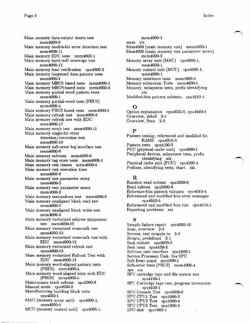
Page 2
Main memory data-output shorts test mem4000-8
Main memory double-bit error detection test mem4000-11
Main memory EDC tests mem4000-1 Main memory hard/soft interrupt test
mem4000-12 Main memory load verification cpu4000-2 Main memory longword data pattern tests
mem4000-1 Main memory MBUS based tests mem4000-1 Main memory MBUS-based tests mem4000-4 Main memory partial word pattern tests
mem4000-1 Main memory partial-word tests (PBUS)
mem4000-4 Main memory PBUS based tests mem4000-1 Main memory refresh test mem4000-8 Main memory refresh test with EDC
mem4000-12 Main memory scrub test mem4000-11 Main memory single-bit error
detection/ correction test mem4000-10
Main memory soft-error log interface test mem4000-9
Main memory subtests mem4000-6 Main memory tag store tests mem4000-1 Main memory test classes mem4000-4 Main memory test execution time
mem4000-8 Main memory test parameter entry
mem4000-2 Main memory test parameter menu
mem4000-2 Main memory test-and-set test mem4000-9 Main memory unaligned block read test
mem4000-9 Main memory unaligned block write test
mem4000-9 Main memory vectorized address uniqueness
test mem4000-12 Main memory vectorized cross-talk test
mem4000-13 Main memory vectorized cross-talk test with
EDC mem4000-13 Main memory vectorized refresh test
mem4000-13 Main memory vectorized Refresh Test with
EDC mem4000-13 Main memory word-aligned pattern tests
(PBUS) mem4000-4 Main memory word-aligned tests with EDC
(PBUS) mem4000-5 Maintenance track subtest spu2000-6 Manual mode cpu4030-2 Manufacturing building block tests
cpu4030-1 MAU (memory array unit) cpu4000-1,
mem4000-1 MCU (memory control unit) cpu4000-1,
mem4000-1 mem xix
Index
Mem4000 (main memory test) mem4000-1 Mem4000 (main memory test parameter menu)
mem4000-2 Memory array unit (MAU) cpu4000-1,
mem4000-1 Memory control unit (MCU) cpu4000-1,
mem4000-1 Memory interleave tests mem4000-6 Memory subsystem Tests mem4000-1 Memory, subsystem tests, prefix identifying
XlX Modified-bits pattern subtests cpu4010-4
0 Option explanation cpu4030-2, cpu4040-3 Overview, dshell 2-1 Overview, Scan 2-3
p Pattern testing, referenced and modified bit
R.Al\1S cpu4010-3 Pattern tests spu4100-3 PCU (physical cache unit) cpu4000-1 Peripheral devices, subsystem tests, prefix
identifying xix Physical cache unit (PCU) cpu4000-1 Prefixes, identifying tests, chart xix
R Random read subtest spu2000-8 Read subtest spu2000-8 Reference-bits pattern sub tests cpu4010-4 Referenced and modified bits error messages
cpu4010-5 Referenced and modified bits test cpu4010-1 Reporting problems xx1
s Sample failure report spu4000-10 Scan, overview 2-3 Screens, test outputs to 2-1 Scripts, predefined 2-1 Seek subtest spu2000-9 Seek tests spu4100-3 Self-test user interface spul000-1 Service Processor Unit. See SPU Soft front panel spul000-1 Soft-error tests (PBUS) mem4000-4 spu xix SPU cartridge tape and file system test
spu4100-1 SPU Cartridge tape test, program invocation
spu4100-1 SPU Console Test spul000-6 SPU CPUl Test spul000-3 SPU CPU2 Test spul000-4 SPU CPU3 Test spul000-5 SPU disk spul000-1
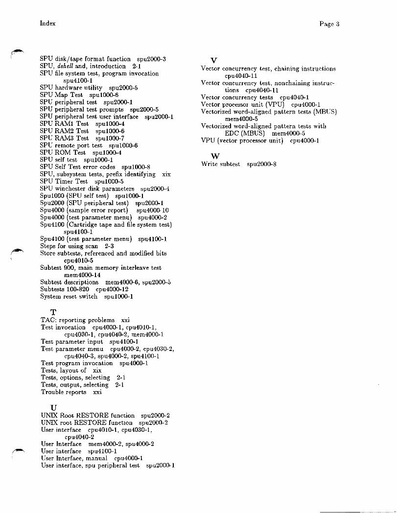
Index
SPU disk/tape format function spu2000-3 SPU, dshel/ and, introduction 2-1 SPU file system test, program invocation
spu4100-1 SPU hardware utility spu2000-5 SPU Map Test spul000-6 SPU peripheral test spu2000-1 SPU peripheral test prompts spu2000-5 SPU peripheral test user interface spu2000-1 SPU RAMl Test spul000-4 SPU RAM2 Test spul000-6 SPU RAM3 Test spul000-7 SPU remote port test spul000-6 SPU ROM Test spul000-4 SPU self test spul000-1 SPU Self Test error codes spul000-8 SPU, subsystem tests, prefix identifying xix SPU Timer Test spul000-5 SPU winchester disk parameters spu2000-4 SpulOOO (SPU self test) spul000-1 Spu2000 (SPU peripheral test) spu2000-1 Spu4000 (sample error report) spu4000-10 Spu4000 (test parameter menu) spu4000-2 Spu4100 (Cartridge tape and file system test)
spu4100-1 Spu4100 (test parameter menu) spu4100-1 Steps for using scan 2-3 Store sub tests, referenced and modified bits
cpu4010-5 Subtest 900, main memory interleave test
mem4000-14 Subtest descriptions mem4000-6, spu2000-5 Subtests 100-820 cpu4000-12 System reset switch spul000-1
T TAC: reporting problems xxi Test invocation cpu4000-1, cpu4010-1,
cpu4030-1, cpu4040-2, mem4000-1 Test parameter input spu4100-l Test parameter menu cpu4000-2, cpu4030-2,
cpu4040-3, spu4000-2, spu4100-l Test program invocation spu4000-1 Tests, layout of xix Tests, options, selecting 2-1 Tests, output, selecting 2-1 Trouble reports xxi
u UNIX Root RESTORE function spu2000-2 UNIX root RESTORE function spu2000-2 User interface cpu4010-1, cpu4030-l,
cpu4040-2 User Interface mem4000-2, spu4000-2 User interface spu4100-1 User Interface, manual cpu4000-1 User interface, spu peripheral test spu2000-l
Page 3
v Vector concurrency test, chaining instructions
cpu4040-11 Vector concurrency test, non chaining instruc-
tions cpu4040-11 Vector concurrency tests cpu 4040-1 Vector processor unit {VPU) cpu4000-1 Vectorized word-aligned pattern tests (MBUS)
mem4000-5 Vectorized word-aligned pattern tests with
EDC {MBUS) mem4000-5 VPU (vector processor unit) cpu4000-l
w Write subtest spu2000-8

THIS PAGE INTENTIONALLY LEFT BLANK

CONVEX Processor Diagnostics Manual (Cl, C120)
Document No. 760-000950-200, Vl .0
Reader's Forum
You are invited to submit comments about the clarity and service of this manual. Constructive critical comments are most welcome, and will help us continue in our efforts to generate quality customer documentation. Please list the document page number with your questions and comments.
From:
Name. __________________ Title. _________________ _
Company ________________ _,_,, ate _________________ _
Address and Phone No·-------------------------------
FOR ADDITIONAL INFORMATION OR DOCUMENTATION:
In Texas (214)952-0200
Other continental locations 1(800)952-0379
Outside continental US Contact local CONVEX office
Direct mail orders to: CONVEX Computer Corporation Customer Service PO Box 833851 Richardson TX 75083-3851 USA
----
(Fold Here First)
_CONVEX
BUSINESS REPLY MAIL FIRST a.ASS PERMIT NO. 1046 RICHARDSON, TEXAS
POSTAGE WILL BE PAID BY ADDRESSEE
CUSTOMER SERVICE CONVEX Computer Corp. P.O. Box 833851 Richardson, TX 75083-3851
(Fold Here Second)
(Tape or Staple)
II I I II NO POSTAGE NECESSARY IF MAILED
IN THE UNITED ST A TE<.;