Embed Size (px)
Citation preview
AD-A096 764 ROCKWELL INTERNATIONAL ANAHEIM CA ELECTRONICS RESEAR--ETC FIG 10/2DEVELOPMENT OF HIGH-EFFICIENCY STACKED MULTIPLE-BANOGAP SOLAR C--ETCU)
UNCASIE C78- 1225.28/IAFWAL-TR-0-2096 NL
nnnmnnmWIIIJIIIIEIB-
11111 I.0 jj 2 .0
III I ll
1111.25 11 1.4 tB1.6
MICROCOPY RESOLUTION TIST CHART
NATIONAL AT of A
] .._ LEVELiC_AFWAL-TR40-206
, DEVELOPMENT OF HIGH-EFFICIENCYSSTACKED MULTIPLE.BANDGAP
tSOLAR CELLS
R. P. RuthJ. S. HarrisP. D. DapkusR. 0. Dupuis
SS. W. Zehr, J. J. Coleman
J. J.TJ. YangD. L. MillerW. I. Simpson EL c,H. T. Yang
Rockwell Intemational ® M 2 4 t eElectronics Research Center3370 Miraloma Ave.Anaheim, California 92803 C
October, 1980
TECHNICAL REPORT AFWAL.TR-80-2096
Interim Report for the Period August 1, 1975 -October 1, 1979
Approved for public release, distribution unlimited
AERO PROPULSION LABORATORYIAIR FORCE WRIGHT AERONAUTICAL LABORATORIES
AIR FORCE SYSTEMS COMMANDWRIGHT.PATTERSON AIR FORCE BASE, OHIO 45433
81 3 24 116
NOTICE
When Government drawings, specifications, or other data are used for any purposeother than in connection with a definitely related Government procurement operation,the United States Government thereby incurs no responsibility nor any obligationwhatsoever; and the fact that the government may have formalated, furnished, or inany way supplied the said drawings, specifications, or other data, is not to beregarded by implication or otherwise as in any manner licensing the holder or anyother person or corporation. or conveying any rights or permission to manufacture,use, or sell any patented invention that may in any way be related thereto.
This report has been reviewed by the Office of Public Affairs (ASD/PA) and isreleasable to the National Technical Information Service (NTIS). At NTIS, it willbe available to the general public, including foreign nations.
This technical report has been reviewed and is approved for publication.
W. 4PATRICK RAHILLY JOSEPH F. WISEProject Engineer TAM, Solar Energy ConversionEnergy Conversion Branch Energy Conversion Branch
FOR THE COMANDER
~I
Chief, Aerospace Power DivisionAero Propulsion Laboratory
"If your address has changed, if you wish to be removed from our mailing list,or if the addressee is no longer employed by your organization, please notifyAFWAL/POOC-2, W-PAFB, OH 45433 to help us maintain a current mailing list".
Copies of this report should not be returned unless return is required by securityconsiderations, contractual obligations, or notice on a specific document.
AIR FORCE/16780/26 rebrUary 1951 - 150

SECURITY CLASSIFICATION OF THIS PAGE (Who. Dole Fn-frld)
READ INSTRUCTIONSREPORT DOCUMENTATION PAGE BEFORE COMPLETING FORM
I REPORT NUMBER 2 GOVT ACCESSION NO, 3. RECIPIENTS CAT*tU UIt7R79 -
AFwA..4rR-8A-9.96' k4 /.4. TITLE (aid XU&Tfltej SX iQ OYREPR&T&P Elw COVERED
I Technical i"eproDevelopment of High-rEfficiency Stacked Multiple.- / 1 Aug 078 *, Oct 1T9.,Bandgap Solar Cells -- 1 A 8 c
C78,Lt-1225. 2/07. AUT6O4a 4 -SOTRACT OR GRANT NUMBER ,
R.P. Ruth, J.il/Harris( P.D./Dapkus R.D.)Dupuis7 / °
S.W. 'Zehr, J. J. Colemtn, J,.J. Yiag,- '33615-78-C-2p36 ""'D.L. Miller, W.I. Simpson and H.T. Yang
9 PERFORMING ORGANIZATION NAME AND ADDRESS '40 PROGRAM ELEMENT. PROJECT vASKAREA & WORK UNIT NUMBERS
Rockwell International Electronics Research Center3370 Miraloma Ave.Anaheim, CA 92803 _
It. CONTROLLING OFFICE NAME AND ADDRESS REPORr2TE
Air Force Wright Aeronautical Laboratories / OctAero Propulsion Laboratory NO,, ,E -a.AG. 6
Wright Patterson AFB, 01 45433 163 7114 MONITORING AGENCY NAME & ADORESS(,f diferen from C nrrn g 0f11-e1 1S SECURI'Y CLASS 'ol rhs repo t
Unclassified
IS. DECLASSIFICATION O*NSRAC:;c, -SCHEDuLE
IS. DISTRIBUTION STATEMENT (of this Report)
Approved for public release; distribution unlimited
17. DISTRIBUTION STATEMENT (of th. aboiract eo f ered nr 8t -k 20. if differnt fro Report,
II. SUPPLEMENTARY NOTES
1 KEY WORDS (Continue on reverse ide i/ necesaary old idernftf hv hl k numberI
Cascade solar cells, multijunction solar cells, Ill-V compound semiconductors,Gallium Arsenide
/
rO AS R Continue on reverae sl ofe I necea..it' and identify by block number)r -month program of a twenty-four month experimental investigation backed by
analytical modeling has been conducted to develop technologies required for fabricatingstacked multiple bandgap solar cell (SMBSC) assemblies having AMO 1-sunefficiencies of 25% or greater at 250C.
Investigations were undertaken with the following four SMBSC materials systems:(1) two-cell GaAs-Ge structure, made by metalorganic chemical vapor deposition (MO-CVD),conventional CVD, and molecular-beam epitaxy (MBE) methods; (2) two-cell GaAs-nGaAs structure, made by liquid-phase cptaxy (LPE) techniaues: (3) three-cell
DO ,*.o. , 1473 EDITION OF I NOV 6 IS OBSOLETE
SECURITY CLASSIFICATION OF THIS PAG mien teFnieredl
-...........1[ ... ... ...
SECURITY CLASSIFICATION OF TIS PAGR(U'Wha DO$*. gn#e*d)
GaAlAs-GaAs-GaAsSb structure, made by MO-CVD and MBE methods; and (4)three-cell GaAeAs-GaAs-InGaAsP structure, made by LPE and MBE methods. Eachof these systems involves the GaAPAs-GaAs materials combination as the basicbuilding block. Near the end of the program a change in emphasis was introduced tolimit the investigations to GaAeAs-GaAs and GaAs-Ge two-cell structures and thethree-cell GaAeAs-GaAs-Ge structure that might also result. Principal em.phasiswas then placed on the MO-CVD technique, supplemented by MBE, LPE, or otherdeposition and/or processing techniques where appropriate.
The principal achievement was with the GaAeAs-GaAs systerm,j in which a two-cellSMBSC that exhibited voltage addition (Voc il.i- V) under illumination was success-fully fabricated. The two individual cells and the connecting tunnel junction weregrown entirely by MO-CVD techniques in this structure. Similar structures made bya combination of MO-CVD and MBE techniques also appeared quite promising.,,,
Two-cell GaAs-Ge assemblies, made by a combination of MO-CVD and conventionalCVD methods or by combined MO-CVD and MBE techniques, were not as successful,although theoretically capable of essentially the same overall efficiency (up to -25 )as the GaA2As-GaAs tandem structure. The other materials combinationsinvestigated in this program received considerably less attention, and correspondingliless progress toward the program goals was made with those structures.
Details of the investigations with all four materials systems are given, andrecommendations for continued work are outlined.
SECURITY CLASSIFICATION OF THIS PAGI~f*h Date Fnte..)
L . .- 4
FOREWORD
This report was prepared by Rockwell International Electronics ResearchCenter Laboratories in Anaheim and Thousand Oaks, California, under contractF33615-78-C-2036.
The work was administered under the direction of W. P. Rahilly, AFWAL/POOC-2, Air Force Wright Aeronautical Laboratories, Aero Propulsion Laboratory,under Project 3145, Task 314519, Development of High-Efficiency Stacked Multiple-Bandgap Solar Cells. The period covered is 1 August 1978 to 1 October 1979.Contributors include L. A. Moudy, K. L. Hess, F. F. Kinoshita, R. E. Johnsonand R. D. Yingling of the Electronics Research Center, Anaheim laboratories, andY. Z. Liu and R. Sahai of the Electronics Research Center, Thousand Oakslaboratories.
Acce"ss'~' vor
D'1C T'.J nirfict lo
Distribution/Availnbility Cod ,s
Avail hnflor
DI Seca
TABLE OF CONTENTS
Section Page
1 INTRODUCTION AND SUMMARY OF RESULTS .............. 1
1.1 Technical Concepts ........................... 11.2 Program Objectives ........................... 51.3 General Technical Approach and Program Rationale ....... 61.4 Summary of Principal Results ...................... 7
2 DETAILED DISCUSSION OF RESULTS .................... 17
2.1 SMBSC Modeling and Analysis ........................ 18
2.1.1 Multilayer AR Coating Design ............... 192.1.2 Ge Solar Cells ......................... 202.1.3 GaAIAs Heteroface Solar Cells ................ 242.1.4 GaAs Window-type Solar Cells ................ 25
2.2 GaAs-Ge SMBSC Technology Development ............... 28
2.2.1 Properties of GaAs-Ge Interface .............. 302.2.2 GaAs Solar Cells for GaAs-Ge SMBSC's ......... 302.2.3 Ge Solar Cells for GaAs-Ge SMBSC's ........... 632.2.4 Connecting Intercell Junction Structures for
GaAs-Ge SMBSC s ....................... 842.2.5 Experimental GaAs-Ge SMBSC Structures ........ 94
2.3 GaAs-InGaAs SMBSC Technology Development ........... 98
2.3.1 InP and InGaAs Layers Grown by LPE ........... 992.3.2 AlGaAsSb Materials System as Alternative for
Low-bandgap Cell ....................... 106
2.4 GaAlAs-GaAs-GaAsSb SMBSC Technology Development .... 113
2.4.1 GaAfAs Solar Cells ........................ 1152.4.2 Connecting Junctions in GaAs and GaARAs o....... 1292.4.3 GaAf As-GaAs Two-cell SMBSCs .............. 132
2.5 GaA#As-GaAs-InGaAsP SMBSC Technology Development 142
2.5.1 LPE Growth of GaAR As on GaAs Substrates ...... 1432.5.2 LPE Growth of InGaAsP ................... 149
2.6 Development of AR Coating Technology o.............. 150
3 SUMMARY AND CONCLUSIONS .o...................... 151
4 REFERENCES ..................................... 162
v
LIST OF ILLUSTRATIONS
Figure Page
1. Schematic Representation of Stacked Multiple-bandgapSolar Cell ....................................... 3
2. Schematic Representation of SMBSC Configuration Inv3lvingBoth Electrical and Optical Series Arrangement ............... 4
3. Tunneling I-V Characteristic for 25x25 mil Mesa Diode inp+GaAs:Zn/n+GaAs:Se Epitaxial Structure Grown by MO-CVDon nGaAs:Si Substrate at 6500 C ......................... 10
4. Configuration of Two-cell GaAlAs-GaAs SMBSC for whichVoltage Addition was Observed under Illumination .............. 11
5. Dark and Illuminated (microscope lamp) I-V Curves for Two-cell SMBSC Grown Entirely by MO-CVD on GaAs:Si Substrate,with Ga0. 7 A10. 3 As Cell and GaAs Cell Connected by Intermediaten-p + Junction in GaAs 12
6. Optimized 3-layer AR Coating Design for AMO Spectrum with4062A CaF2 Top Layer, 838A SiO 2 Middle Layer, and 591.1TiO2 Bottom Layer for 0.3-1. lum Operation (3-cell SMBSC)and Minimum Integrated Reflection Loss ................... 21
7. Optimized 3-layer AR Coating Design for AMO Spectrum with1810A MgF 2 Top Layer, 919A Si0 2 Middle Layer, and 1296ATiO2 Bottom Layer, for 0. 3 -1. 8um Operation (2-cell or4-cell SMBSC) and Minimum Integrated Reflection Loss .......... 21
8. Optimized 3-Layer AR Coating Design for AMO Spectrum with1756A MgF2 Top Layer, 1340A SiO2 Middle Layer, and 835ATa 2 0 5 Bottom Layer, for 0.3-1.8pm Operation (2-cell or4-cell SMBSC) and Maximum Short-circuit Current for CellAssem bly ........................................ 22
9. Calculated Internal Photoresponse (charge collectionefficiency) for Ge Solar Cell of Specified Parameters ............ 22
10. Calculated Internal Photoresponse (charge collectionefficiency) for Thin Ge Solar Cell with and without Back-surface Field As3ociated with n-n + Junction at Back of Cell ...... 24
11. Measured and Calculated Photoresponse Data for As-grownGaMAs Solar Cell of Sample LPE1011, Based on CorrectedExperimental Photoresponse Curve and Computer ModelUsing Parameters of Table 3 ........................... 26
12. Two Possible Configurations of GaAs-Ge Two-cell SMBSCAssembly ........................................ 29
13. Photograph of Typical Array of 0.5 cm x 0.5 cm GaA2 As-GaAsCells Grown by MO-CVD and Fabricated on Single-crystalGaAs Substrate -3.7 cm x 2.1 cm ....................... 32
14. Illuminated (microscope lamp) I-V Characteristics ofConventional GaAlAs-GaAs Thin-window Heteroface SolarCell Structure Grown by MO-CVD at 7500 C on GaAs Single-crystal Substrate, Showing Effect on Fill Factor of CenteringIllumination (a) Near Metal Contact Pad at Edge of0.5cm x 0.5cm Cell, and (b) Near Opposite Edge of Cell ......... 33
vi
LIST OF ILLUSTRATIONS (Cont)
Figure Page
15. Dark and Illuminated (microscope lamp source) I-V Character-istics of GaA2As-GaAs Window-type Solar Cell Grown by MO-CVDon Single-crystal GaAs:Si Substrate Early in Phase 1 Program ... 34
16. Dark and Illuminated (microscope lamp) I-V Characteristics of0.5cm x 0. 5cm GaARAs-GaAs Window-type Solar Cell Depositedby MO-CVD at- 750 0 C on (100) GaAs:Si Substrate Midwaythrough Phase 1 Program ............................ 35
17. Dark and Illuminated (microscope lamp) I-V Characteristicsof GaACAs-GaAs Thin-window Heteroface Solar Cell Grownby MO-CVD at 7500C on (100) GaAs:Si Substrate ............. 37
18. Dark and Illuminated (xenon lamp AMO simulator, 135 mw/cm2 )I-V Characteristics of GaARAs-GaAs Thin-window HeterofaceSolar Cell grown by MO-CVD at 7500C on Same (100) GaAs:SiSubstrate as Cell of Figure 17 ......................... 37
19. Dark and Illuminated (microscope lamp) I-V Characteristics ofConventional Thin-window GaA2 As-GaAs Heteroface Cell(0.5cm x 0.5cm) Grown by MO-CVD at -700 0 C on Single-crystal GaAs:Te Substrate ........................... 39
20. Dark and Illuminated (microscope lamp) I-V Characteristics ofConventional Thin-window GaAe As-GaAs Heteroface Cell(0.5 cm x 0.5 cm) Grown by MO-CVD at -750 0 C on Single-crystalGaAs:Te Substrate ................................ 39
21. Dark and Illuminated (microscope lamp) I-V Characteristics ofThin-window GaAe As-GaAs Heteroface Solar Cell (0.5cm x0.5cm) Grown by Mvq-CVD at -750 0 C on Single-crystalGaAs:Te Substrate; Both Window Layer and p-type ActiveLayer Thinner than Usuel ............................ 40
22. Fourth-quadrant I-V Characteristic of GaA As-GaAs Window-typeHeteroface Solar Cell (0.5cm x 0.5cm) Made by MO-CVD, underSimulated AMO Illumination of 129 mw/cm 2 from CalibratedSimulator ...................................... 40
23. Dark and Illuminated (microscope lamp) I-V Curves of Ti'wo Con-ventional GaAeAs-GaAs Thin-window Heteroface Solar Cells(0.5cm x 0.5cm) Grown by MO-CVD at 750 0 C on Different Single-crystal GaAs Substrates after Recalibration of Mass FlowController ................. ...................... 42
24. Spectral Response Data for Two Different GaAi As-GaAsHeteroface Solar Cells (0.5cm x 0.5cm) Processed in MO-CVDLayers Grown at 7500 C on One GaAs Substrate Wafer ............ 43
25. Dark and Illuminated I-V Characteristics of GaAs p-n JunctionMesa Diodes (50 mil x 50 mil) Grown by MO-CVD on n-type(100)Ge Substrates; a) Uncoated Substrate; b) Substrate Coatedwith S1O 2 . . . . . . . . . . . . . . . . . . . . . . . . . . . . . . . . . . . . . . . 46
26. Dark and Illuminated I-V Characteristics of GaAe As-GaAs SolarCells Grown by MO-CVD at 700 0 C Simultaneously on a) Single-crystal (100)GaAs:Si Substrate and b) Single-crystal (100)Ge:SbSubstrate with si0 2 Coating ........................... 47
vii
LIST OF ILLUSTRATIONS (Cont)
Figure Page
27. Forward Dark I-V Characteristics of GaAP As-GaAs Solar CellsGrown by MO-CVD on GaAs:Si Substrates and Processed intoCompleted Devices a) in Sixth Month of Program and b) Earlyin Program ...................................... 48
28. Dark and Illuminated (microscope lamp) I-V Charcteristicsof GaAi As-GaAs Heteroface Solar Cells (0.25 cm area)Grown by MO-CVD at -690 0 C on a) (100) Ge:Sb Single-crystalSubstrate and b) (100) GaAs:Si Single-crystal Substrate .......... 50
29. Dark and Illuminated (microscope lamp) I-V Characteristics ofGaA As-GaAs Heteroface Solar Cells (0.25 cm 2 area) Grown byMO-CVD at -700 0 C on a) (100) Ge:Sb Single-crystal Substrateand b) (100) GaAs:Si Single-crystal Substrate, with DifferentPredeposition Conditions in Reactor Chamber from ThoseUsed for Cells of Figure 28 ........................... 51
30. Dark and Illuminated (microscope lamp) I-V Characteristics ofGaAeAs-GaAs Thin-window Heteroface Solar Cell (0.5cm x0.5cm) Grown by MO-CVD at 7500 C Using "Non-standard"Predeposition Procedure on a) Ge:Sb Substrate andb) GaAs:Si Substrate ............................... 53
31. Dark and Illuminated (microscope lamp) I-V Characteristics ofGaA2 As-GaAs Thin-window Heteroface Solar Cell (0.5cm x 0.5cm)Grown by MO-CVD at 750 0 C on Ge:Sb Substrate Using StandardPredeposition Procedure ............ ...... 54
32. Dark and Illuminated (AMO simulator, -135 mw/cm 2 ) I-VCharacteristics of Another GaAeAs-GaAs Thin-window HeterofaceSolar Cell (0.5cm x 0.5cm) Fabricated on Same Ge'Sb Substrateas Cell of Figure 31 ................................ 54
33. Fourth Quadrant of Illuminated (AMO simulator) I-V Curve forMO-CVD GaAs Heteroface Solar Cell (0.5cm x 0.5cm) Grownat -750 0 C on (100)Ge:Sb Substrate, Using Standard Pre-AsH3Procedure ...................................... 56
34. Fourth Quadrant of Illuminated (AMO simulator) I-V Curve forMO-CVD GaAs Heteroface Solar Cell (0.5cm x 0.5cm) Grownat -750 0 C on (100)Ge:Sb Substrate Using NonstandardFre-AsH3 Procedure ............................... 57
35. Spectral Response Curves for GaAs Heteroface Cells Made byMO-CVD on GaAs and Ge Substrates; Junction Depths NominallyEqual in Both Cells ................................ 59
36. Illuminated (AMO simulator) I-V Curve for GaAs HeterofaceSolar Cell (area 0.025 cm 2 ) Grown by MBE at -580 0 C on(100) GaAs Substrate ............................... 60
37. Illuminated I-V Curves for GaAs n/p Solar Cell Structure (area0.025 cm 2 ) Grown by MBE on n-type (100) Ge Substrate, forSeveral Different Levels of Illumination from Microscope Lamp .. 61
38. Spectral Response Curve for MBE-grown Device of Figure 37,Showing Photoresponse of Opposite Sense for n/p GaAs Junctionand pGaAs-nGe Heterojunction ......................... 62
viii
LIST OF ILLUSTRATIONS (Cont)
Figure Page
39. Dark and Illuminated (microscope lamp source) I-V Character-istics of Ge p-n Junction Mesa Diode Grown by MO-CV D onSingle-crystal Ge:Sb Substrate ......................... 64
40. Dark and Light (microscope lamp source) I-V Characteristicsot Cc p-n Junction Solar Cell Grown by GeH 4 Fyrolysis onSingle-crystal (100)Ge:Sb Substrate ..................... 65
41. Dark and Light (microscope lamp source) I-V Characteristicsof Ge p-n Junction Mesa Diode Grown by GeH4 Pyrolysis onSingle-crystal (100)Ge:Sb Substrate ..................... 66
42. Resistivity as Function of Depth into Sample as Obtained bySpreadiag Resistance Probe Scan on Beveled Surface in Two-layer CVD Ge Film Grown at 650 0 C on n-type GaAs Surface;p-n Junction Shown Is at Interface between p-type and n-typeGe Layers ...................................... 68
43. Dark and Illuminated (microscope lamp) I-V Curves for Gep-n Junction Mesa-type Solar Cell Grown by CVD at-680 0 C on GaAs:Te Substrate ......................... 70
44. Dark and Illuminated (microscope lamp) I-V Curves for Gep-n Junction Solar Cell (0.5 cm x 0.5 cm) Grown by CVD at-680 0 C on Ge:Sb Substrate ........................... 70
45. Spreading Resistance Data for Undoped Ge Films Grown by CVDon Single-crystal Substrates of n-type (100)Ge:Sb in TwoSeparate Deposition Experiments, Showing Effects of PossibleGa Doping of Ge Films; a) Deposition Temperature 7501C,Deposition Time 60 min; b) Deposition Temperature -760 0 C,Deposition Time 230 min ............................ 72
46. Spreading Resistance Data (as function of depth) for B-dopedp-type Ge Film Grown by C VD at 800 0 C on Substrate ofSingle-crystal n-type (0.02-0.03 ohm-cm) Ge:Sb ............ 73
47. Dark and Illuminated (microscope lamp) I-V Curves for Gep-n Junction Solar Cell (0.5 cm x 0.5 cm) Formed by p-typeB-doped Ge Deposition (CVD) on n-type Ge:Sb (0.03 ohm-cm)Substrate at 800 0 C at Rate of -1900 A/min................... 75
48. Fourth Quadrant of Illuminated (AMO simulator) I-V Curve forGe CVD Cell No. 75-7, Grown at -800 0 C on (100)-orientedn-type 0.03 ohm-cm Ge Substrate Wafer ..................... 78
49. Dark Forward I-V Curve for Ge CVD Cell No. 75-7 ............ 7950. Relative Spectral Photoresponse of CVD Ge Solar Cells No. 75-7
and No. 73-11 ................................... 8051. Fourth Quadrant of Illuminated (AMO simulator) I-V Curves
for CVD Ge Solar Cell No. 79-9 before and after ContactAlloying Procedure ................................ 81
52. Dark and Illuminated (AMO simulator) I-V Curves Obtained forCVD Ge Cell No. 73-11 after Contact AlloyingProcedure, Showing Gradual Shift in Illuminated Curve overPeriod of -15 sec following Exposure to Light ................. 81
ix
LISIT OF ILLUSTRATIONS (Cont)
Figure Page
53. Dark and Illuminated (microscope lamp) I-V Curves forSolar Cell (area 6.6 x 10- 3 cm 2 ) Formed by Diffusing MBE-deposited As into p-type (100)Ge Substrate, Showing Effectof Variation of Incident Intensity ........................ 83
54. Relative Spectral Photoresponse for n/p Ge Solar Cell Madeby MBE Deposition of As onto p-type (100)-oriented GeSubstrate Wafer Followed by Thermal Diffusion of the As ........ 8:3
55. Spreading Resistance Data for n-type Ge Single-crystal Waferwith p-n Junction 2.0[m Deep Formed by Diffusion of Ga at8500C for 5 hr in He, Using Spin-on Oxide Diffusion Source ..... 85
56. Tunneling I-V Characteristic for 25x25 mil Mesa Diode inp+GaA s :Z n/n+GaA s :Se Epitaxial Structure Grown by MO-C VDon nGaAs:Si Substrate at 650 0 C ........................ 86
57. I-V Characteristic of GaAs:Se/GaAs:Zn n+/p + Tunnel JunctionStructure Grown by MO-CVD at -650 0 C on GaAs Single-crystalSubstrate ............................ 87
58. I-V Characteristic of GaAs:Se/GaAs:Zn n+/p + Tunnel JunctionStructure Grown by MO-CVD at -6300C on GaAs Single-crystalSubstrate ........ .............................. 88
59. I-V Characteristic of n+/p + GaAs:Se/GaAs:Be Hybrid TunnelStructure Made by Growing MO-CVD Layer on PreviouslyGrown MBE Layer on Single-crystal GaAs Substrate ............ 89
60. Dark Log I-V Curve for Hybrid MO-CVD/MBE n+GaAs/p+GaAsTunnel Junction Structure on GaAs Substrate .................. 89
61. Dark Log I-V Curve for n+GaAs/p+GaAs Tunnel JunctionStructure Grown Entirely by MO-CVD on GaAs Substrate ....... 90
62. I-V Characteristic of p+/n + GaAs:Zn/GaAs:Se Tunnel DiodeStructure Grown by MO-CVD at -630 0 C on Single-crystalGaAs Substrate ................................... 91
63. Configuration of n+/p + + Conducting Junction StructureFormed by MBE on Single-crystal GaAs Substrate at -540 0 C .... 92
64. Typical Forward and Reverse Oscilloscope Trace Obtainedwith n+/p ++ GaAs Conducting Junction Structure Grown byMBE at -540 0 C on p+GaAs:Zn Substrate, Showing OhmicBehavior ............................ ......... 92
65. Forward and Reverse I-V Characteristics of nI/p+ GaAsConducting Junction Structure of Figure 64 Grown by MBEat -5400C on p+GaAs:Zn Substrate, after TemperatureCycling Duplicating that Encountered in LPE Cell Growth ...... 94
66. Forward and Reverse I-V Characteristics of n/n+/p+/p GaAsConducting Junction Structure Grown by MBE on p+GaAs:ZnSubstrate (a) before and (b) after Temperature CyclingDuplicating that Encountered in LPE Cell Growth .............. 95
67. Probable Configuration of GaAs-Ge Two-cell SMBSC MadeEntirely by CVD Techniques .......................... 96
x
LIST OF I LLUS I RATIONS (Cont)
Figure Page
68. Spectral Response Curve for MBE-grown Stacked Two-cellStructure IHaving Apparent ConfigurationpGa 0 ,A, As/nGaAs/n GaAs/p GaAs/nGe .... .............. 97
G9. Spectr. Photresponse of LPE InGaAs p-n Junction Cellwith Illumination Incident through Inil Substrate ................. 101
70. Dark and Illuminated I-V Characteristics of InGaAs p-nJunction Measured with Microscope Lamp Illumination ........... 102
71. Dark and Illuminated (microscope lamp) I-V Curves Obtainedfor Different Intensities of Illumination for InP/InGaAs SolarCeil (0.025 cm x 0.025 cm) Obtained by LIPE Growth of Undopedn-type InGaAs Layer on Single-crystal p+InPl Substrate Wafer .... 105
72. Relative Spectral Response Curve for InP/InGaAs Window-typeSolar Cell Grown by LPE ............................. 106
73. Dark and Illuminated (AM1 simulator) I-V Characteristics ofpGaSb/nGaSb Solar Cell (area 0.025 cm 2 ) a) with A GaAsSbWindow Layer and b) without Window Layer ................. 108
74. Spectral Response of pAiGaAsSb/pGaSb/nGaSb Window-typeSolar Cell of Figure 73a. . ........................... 109
75. Dark and Illuminated (AM1 simulator) I-V Characteristics ofLPE-grown p+GaA AsSb/pGaAR Sb/nGaSb Window-type SolarCells ......... .......................................... 111
76. Dark and Illuminated (microscope lamp source) I-V Character-istics of 50 nil x 50 mil Mesa Diode Fabricated inGao. 6 3A 0.37As p-n Junction Structure Grown by MO-CVD on(100)GaAs Substrate ................................ 116
77. I-V Characteristic of p-n Junction Mesa Diode in Ga0. 6 A 0.4AsStructure Grown by MO-CVD on GaAs:Si Substrate ............... 116
78. Dark and Illuminated (microscope lamp) I-V Curves [or Thin-window Solar Cell (0.5cm x 0.5cm) in Ga0.6A0.4 As Grownby MO-CVD at 7000 C on GaAs:Te Substrate .................... 117
79. Configuration of Ga 0 *7Ae 0. 3 As Window-type Solar CellStructure Grown by MO-CVD on GaAs Substrate ................. 118
80. Dark and Illuminated (microscope lamp) I-V Curves forWindow-type Ga 0* 7 A2 0 , 3 A s p-n Junction Solar Cell(0.5cm x 0.5cm) Grown by MO-CVD at -790 0 C onGaAs:Te Substrate ................................. 119
81. Dark and Illuminated (microscope lamp) I-V Curves for0.5cm x 0.5cm Window-type Gao. 7 A0. 3 As p-n JunctionSolar Cell Grown by MO-CVD at 750 0 C on GaAs Substrate ......... 120
32. Spectral Response Data for Two 0.5cm x 0.5cm Ga0 . 7 Ate 0 . 3 AsAlloy Solar Cells Grown by MO-CVD at 750 0 C on Common
GaAs:Si Substrate ...... ............................ 12183. Dark and illuminated (microscope lamp) I-V Curves for Window-
type Gao.76Ae 0.2 4 As p-n Junction Solar Cell (0.5cm x 0.5cm)Grown by MO-CVD at -750oC on (100)GaAs:Te Substrate .......... 122
xi
LIST OF ILLUSTRATIONS (Cont)
Figure Page
84. Illuminated I-V Curve (fourth quadrant) of Gao. 76A2 0. 2 4 AsSolar Cell from Same Array as that of Figure 83 butObtained with AMO Simulator .......................... 123
85. Dark and Illuminated (microscope lamp) I-V Curves forWindow-type Ga0 . 7 A 0 . 3 As p-n Junction Solar Cell(0.5cm x 0.5cm) Grown by MO-CVD at -790 0 C on(100)GaAs:Si Substrate ............................... 124
86. Measured Voc Values for MO-CVD Alloy Cells of Tables 8and 9 as Function of Deduced A Content of Junction-formingLayers, for Simulated AMO Illumination ..................... 128
87. Dependence of Jsc upon Junction Depth (p layer thickness) forThree Ga 0 . 8 Ae 0. 2 As Solar Cells Made by MO-CVD, forSimulated AMO Illumination ............................. 128
88. Spectral Response Curves for Three MO-C VD GaO. 8A 0.2A sCells of Different Junction Depths (p layer thickness) .......... 130
89. Spectral Photoresponse Curves for GaAfAs Solar Cells Made inMO-CVD Structures Having Different GaAe As Window-layerCompositions, Processed Both in As-grown Condition and withZn Diffusion ..................................... 130
90. Configuration of Two-cell SMBSC Grown by MO-CVD on GaAsSingle-crystal Substrate, with Connecting Junction in GaAR As .... 132
91. Dark and Illuminated (microscope lamp) I-V Characteristicsof Two-cell SMBSC Grown by MO-CVD, with Gao. 6 A2 0.4AsCell and GaAs Cell Connected by Intermediate n+-p + Junctionin Ga 0 . 9 2 Ae 0 . 0 8As ... ............................. 133
92. Dark and Illuminated (microscope lamp) I-V Characteristics ofTwo-cell SMBSC Grown by MO-CVD, with Gao.6A2 0.4As Celland GaAs Cell Connected by Intermediate n+-p + Junction inGaAs .......................................... 134
93. Dark and Illuminated (microscope lamp) Reverse I-VCharacteristics of Two-cell Ga 0 . 6 AP 0o 4 As-GaAs SMBSCRepresented in Figure 92 ............................ 134
94. Configuration of Two-cell GaA2 As-GaAs SMBSC for whichVoltage Addition was Observed under Illumination .............. 135
95. Dark and Illuminated (microscope lamp) I-V Curves for Two-cell SMBSC Grown Entirely by MO-CVD on GaAs:Si Substrate,with Gao. 7AR0. 3As Cell and GaAs Cell Connected by Inter-mediate n+-p + Junction in GaAs ........................ 136
96. Modified Configuration of Two-cell GaAe As-GaAs SMBSCStructure Grown by MO-CVD .......................... 137
97. Dark and Illuminated (microscope lamp) I-V Curves for Two-cell SMBSC Grown Entirely by MO-CVD on GaAs:Si Substrate,with Ga 0 7 Ae 0. 3 As Cell on Top and GaAs Cell on BottomConnected by Conducting n+-p + Junction in GaAs IntermediateLayer .......................................... 137
xii
LIST OF ILLUSTRATIONS (Cont)
Figure Page
98. Dark and Illuminated (microscope lamp) I-V Curves forTwo-cell SMBSC (0.5cm x 0.5cm) Grown by MO-CVD on GaAs:S1Substrate, with Ga 0 . 7 A 0 . 3 As Cell on Top (grown at -775 0 C) andGaAs Cell on Bottom, Connected by n+/p+ Conducting Junctionin GaAs Intermediate Layer Grown at -710oC.................. 138
99. Configuration of Two-cell GaAP As-GaAs SMBSC Used toProduce Photoresponse of Figure 100 .................... 139
100. Dark and Illuminated (microscope lamp) I-V Curves for Two-cellSMBSC Grown by MO-CVD on GaAs:Si Substrate, withGa0.7A2 0. 3 As Alloy Cell on Top and GaAs Cell on BottomConnected by Conducting n+/p + Junction in GaAs IntermediateLayer ......................................... 139
101. Modified Two-cell GaMe As-GaAs SMBSC ConfigurationDesigned to Give Improved Performance .................... 140
102. Fourth Quadrant Illuminated (AMO simulator) I-V Curve for Two-cell SMBSC Made by MO-C VD, Consisting of GaAP As Cell onGaAs Tunnel Junction on GaAs Cell, All on (100)-orientedGaAs:Si Substrate ................................. 141
103. Three GaAeAs Large-bandgap Solar Cell Structures Grown byLPE Techniques, for Eventual Use in Two-cell and Three-cellSMBSC Is . ...................................... 145
104. Typical a) Illuminated I-V Characteristic and b) Dark log I-VCharacteristic of Zn-diffused-junction Window-typeGa 0 , 6 1AI 0.39As Solar Cell Grown by LPE (Type b, Figure 103) 146
105. Typical Spectral Photoresponse of Zn-diffused-junction Window-type Ga 0 . 6 1A0. 3 9 As Solar Cell Grown by LPE (Type b,Figure 103) ..................................... 147
106 Typical 770 K Photoluminescence Data for Conventional LPE-grown Window-type Gao. 6 1 A10. 3 9 As Solar Cell (Type a,Figure 103) ..................................... 147
107 Spectral Response Curves for Zn-diffused Heteroface CellLPE1009 and As-grown Heteroface Cell of Sample LPE1011 ...... 149
xiii
_I
LIST OF TABLES
Table Page
1. Calculated Ideal and Expected AMO Efficiencies forSMBSC Combinations with Two, Three, or Four Cells .............. 5
2. Combinations of Materials and Film-growth TechniquesSelected for Initial Development in Phase 1 of Program .............. 7
3. Parameters Used in Modeling Spectral Photoresponse ofLPE-grown Solar Cell (Sample LPE1011) ................... 26
4. Principal Deposition Parameters, Materials Properties,and AMO (no AR coating) Photovoltaic Performance Param-eters of CVD Ge p/n Solar Cell Structures Grown on GeSubstrates ......................................... 77
5. Structural Parameters and Electrical Properties of GaAsNonrectifying Junction Structures Grown by MBE, beforeand after Temperature Cycling .......................... 93
6. Material, Fabrication, and Typical Individual Cell PhotovoltaicPerformance Parameters for Window-type Solar Cell StructuresGrown by LPE on n-type GaSh Single-crystal Substrates ........... 110
7. Summary of Materials and Fabrication Parameters Used inInvestigation of Various Ohmic Contacts to p-type and n-typeGaSb ............................................ 112
8. Principal Physical Parameters of GaAJAs Heteroface SolarCell Structures Grown by MO-CVD and Processed in FinalTwo Months of Phase 1 ................................ 126
9. Measured Photovoltaic Properties of MO-CVD GaAfAs Hetero-face Solar Cells Listed in Table 8 (AMO simulated illumination) .... 127
10. Principal Physical Parameters of LPE GaAfAs HeterofaceSolar Cell Structures ................................. 145
11. Measured Photovoltaic Properties of LPE-grown GaAIAsHeteroface Solar Cells Listed in Table 10 (AMO simulatedillum ination) ....................................... 148
xv
1. INTRODUCTION AND SUMMARY OF RESULTS
In recent years, technology developments for the fabrication of high-efficiencysolar cells have led to the demonstration of laboratory-type Si and GaAs cells havingair-mass-zero (AMO) power conversion efficiencies greater than 15 and 17 percent,respectively. Achievement of significantly higher efficiencies for operation with thespace solar spectrum is becoming increasingly important to the Air Force as spacepower supply performance requirements are increased and the need for weight andcost reductions becomes more evident.
The highest achievable AMO efficiency for Si solar cells is expected to be in the16-19 percent range, and the highest efficiency for GaAs cells is expected to beapproximately 20-22 percent. Thus, the achievement of solar cell conversion effi-ciencies greater than 25 percent will require a combination of semiconductor mate-rials processed in some manner such that the resulting devices will have a broaderresponse to the space solar spectrum than that of any of the simple (single -junction)cells. It is anticipated that such a device, in its simplest form, will be monolithicand consist of at least two sub-cell structures of differing bandgap energy connectedelectrically in series.
The program described in this report is directed toward such a development.
This section of the report describes the basic technical concepts involved,defines the program objectives, outlines the general technical approach employed,and gives a summary of the principal technical results achieved in the first phase(14 months) of the contract.
Section 2 outlines the program plan and schedule followed during the first 14months of the contract, defines the specific technical tasks that constitute the pro-gram, and contains a detailed discussion of the technical activities of Phase 1 and ofthe results achieved in the period covered by this report.
Section 3 contains a brief discussion of the results and of the conclusionsreached therefrom, with recommendations for continued work in Phase 2 of thecontract.
Section 4 lists the technical references used throughout the report.
1.1 TECHNICAL CONCEPTS
The GaAs solar cell - whatever specific configuration is involved - is believedto offer the highest ultimate AMO conversion efficiency of all of the single-componentphotovoltaic cells developed to the present time, based both on theoretical analysesof the photovoltaic effect at potential barriers in semiconductor materials and on thepresent state of development of the respective material technologies. However, theprospect of a dramatic increase in cell operating efficiency, even with respect to thepresent high value of -'19 percent (AMO, 28 0C) achieved in the best single-crystalGaAs cells, is offered by the concept of the tandem multilple-bandgap solar cell.
Ilheoretical analyses by various investigators Mels 1, 2 1 have show n that thenltxiilUlil C'o) r '.SiOl effiticiency for the solar slectruim that can be expected1 from anvMle li-ni junction type of photovoltaic cell operatiarg at its mLximuf lio%4er Ifl ntiat -25'0(1 is in the 20 to 25 percent range, the specific theoretical maximum depend-ig primarily ullon the bandgap energy .:g of the particular semiconductor involved.
Analyses of the projected performance of Si and GaAs solar cells under AMO i llumi -nation indicate expected maximum solar conversion efficiencies of about P)D percentfor Si and perhaps up to 22 percent for GaAs, with all controllable parametersoptimized.
(oncentration of stulilght to pro(duce illumination of increased intensitv is onemethod of achieving increased electrical power output per unit area of solar cellsurface. flowever, the approach to more efficient use of the solar spectrum that isaddressed in this program is based on the fact that a photovoltaic cell has two majorlimitations on its ability to convert the incident solar photons, each of energy hv.into hole-electron pairs that can subsequently he separated, collected, and deliveredto an external load. I'he first is that only those absorhed photons of energN' greaterthan the banidgap energy Eg can produce hand-to-hand excitation in the semiconductorand thus separation of charges and possible delivery to the load. The second is thatall photon energy in excess of the bandigap energy l.g - that is, all of the energybeyond that requi red to produce a si rgle hole-elect ron pair - is di ssiprated internalivas heat in the device.
The most efficient response of a p-n junction cell is to photons of energv justexceeding the bandgap energy, so if two or more solar cells of differirig handgal ,energy (and thus of different comicsitioni could be arranged appropriately to sharethe solar spectrum, with each opseratinrg onl that I rtior oif the spectrum to which it ismost reslonsive, a combination converter of overall jxnm er efficiency exceedinrg thatof the individual cells used separately ilr the full solar spectrum could he realized.This concept is not newv, having been first proilosed bly .ackson ilef 3' in 1P55 andexamimed by various workers at intervals since that time Hlefs 1, 5,.
There are tN'o princilpal embodimenits of this concept. (nint, involves inrterl' osiligdichroic" mirrors or filters i.e. , beam splittersi i, the incident beam of solar radi-ation so that selected radiation of a pXrtion of the spectrum is diverted to a sola rcell \whose properties (mainly handgap energy V.Pgl allow% it to make relativelv effi-cient use of that selected band of radiation, while allowing the remnairider ,it thespectrum to pass on to a second filter/mirror, which again selects a pilrion of thespectnm to direct onto a second cell of handgap energy l.gw., \"hile tr:rnsmittirig theremainder to a third cell ior a third filter/mirrori, and so on.
The other modification of the multiple-cell concept - and the one with potentialmajor impact on space applications - is shown schematically in Figure 1. It can no\be seriously considered for practical applications primarily because of the remark-able progress made in thin-film photovoltaic material technologies in the past severalyears. It involves two or more solar cells of differing composition land thus differ-ing bandgap energies) used optically in series, in a tandem or stacked arrangement.The cell of largest bandgap energy EgI receives the full solar spectrum incident onits front surface, generating charge pairs from the energy of the absorbed photons ofenergy greater than EgI and transmitting the radiation of energy < IgI on to the
2

~11
LOAD LOAD LOAD
INCIDENT --SOLAR .. ,--RADIATION I I-IENERGY hy I --,.
p n p n p n
CELL NO 1 CELL NO 2 CELL NO 3(E9 1) IE921 IE93 )
E9,> E92 > E93
Figure 1. Schematic Iepresentation of StackedMulti ple-handgap Solar Cell
seco)nd cell, of handgal) :.,2, which utilizes the narrowed band of energies to gener-ate ihotcvoltage and photocurrent consistent with its photovoltaic properties andtransmits the remaining radiation of energy < Eg) on to the third cell, if used, andSO 00.
,.lthough simple in concept, the stacked multi ple-bandga 1) solar cell (S.MHS('inI(l\ cs diffi cult material problems and design and fabrication complexities. Amajor l)roblem to be solved is the question of the design of the interface between theback side of the first component and the front side of the cell next in tine in the stack.Should the photon-generated current of each cell be extracted separately, as shownIn Figure 1, or should the electrical contact he made simplv a series connection,\%ith the current leaviCIg the first cell entering the second cell directly - conceptuallythe simplest structure, and sho%n in Figure 2? In the latter instance it becomesnecessary to match phtocurrents of tile two a(ljoinii ng cells at their operating points,not the short-circuit currentsi, and this requirement alone is accompxanied by majordifficulties of both material selection and interface design. However, this arrange-meit is bV far the more attractive, since it makes maximum use of the compactnessa nd labrication advantages of monolithic thin-filin semiconductor technologies.
Simplified theoretical models of SMI4S(" configurations can give rise to a vari-etv of lIossibl)1' cell comhinations fmore correctlv, p)ossihle combinations of handgapenergies) that appear to offer very attractive combined conversion efficiencies - someap1iproaching the pirobable theoretical upper limit of to to 50 percent for solar conver-sion efficiency for a semiconductor-based converter system having -io loss of theexcess photon energy Mef bil.
3- "- M
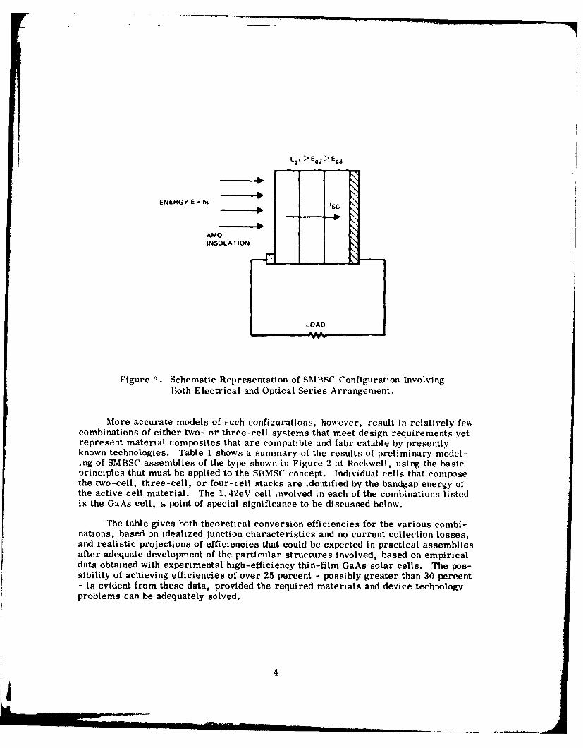
E9 1 > Eg2> Eg3
ENERGY E hv Isc
AMOINSOLATION
LOAD
Figure 2. Schematic Representation of SMBSC Configuration InvolvingBoth Electrical and Optical Series Arrangement.
More accurate models of such configurations, however, result in relatively fewcombinations of either two- or three-cell systems that meet design requirements yetrepresent material composites that are compatible and fabricatable by presentlyknown technologies. Table 1 shows a summary of the results of preliminary model-ing of SMBSC assemblies of the type shown in Figure 2 at Rockwell, using the basicprinciples that must be applied to the SBMSC concept. Individual cells that composethe two-cell, three-cell, or four-cell stacks are identified by the bandgap energy ofthe active cell material. The 1.42eV cell involved in each of the combinations listedis the GaAs cell, a point of special significance to be discussed below.
The table gives both theoretical conversion efficiencies for the various combi-nations, based on idealized junction characteristics and no current collection losses,and realistic projections of efficiencies that could be expected in practical assembliesafter adequate development of the particular structures involved, based on empiricaldata obtained with experimental high-efficiency thin-film GaAs solar cells. The pos-sibility of achieving efficiencies of over 25 percent - possibly greater than 30 percent- is evident from these data, provided the required materials and device technologyproblems can be adequately solved.
4
lITable 1. Calculated Ideal and Expected AMO Efficiencies
for SMBSC Combinations with Two,Three, or Four Cells
Efficienc %1
Two Cells Three Cells Four Cells
Ideal Expected Ideal Expected Ideal Expected Ideal Expected71 T 71 Ti T1 T? 17
Bandlap Energy
2.0 IV 20.0 14.9 20.0 14.9 20.0 14.9
1.42 eV(GaAs) 26.4 19.8 13.0 9.7 13.0 9.7 13.0 9.7
1.0 IV 7.8 5.6 7.8 5.6
0.8 eV 7.5 4.9 3.5 2.3
Combined 17 33.9 24.7 33.0 24.6 40.8 30.2 44.8 32.5
1.2 PROGRAM OBJECTIVES
The overall objective of this program is to develop the necessary technologyto fabricate solar cell assemblies having greater than 25 percent power conversionefficiencies at 25 0 C under space-sunlight illumination of one-sun intensity (AMO,-135 mw/cm 2 ).
To achieve this overall objective the following specific technical objectiveswere defined at the start of the program:
1. Develop and apply rigorous analytical modeling techniques for predictingthe performance of SBMSC structures under AMO operation.
2. Identify and prepare suitable semiconductor, electrical contact, and anti-reflection (AR) coating materials for use in fabricating SMBSC structuresinvolving four (or more) different combinations of semiconductor materialsand/or fabrication techniques.
3. Demonstrate and develop an optimized fabrication technology capable ofproducing large-area (at least 2x2 cm) SMBSC structures exhibiting thespecified performance characteristics.
4. Utilize the selected technology for the fabrication of 2x2 cm stackedmultiple-bandgap cell assemblies.
5. Test and document the photovoltaic performance and certain radiationdamage properties of the fabricated cell assemblies.
The general technical approach used to pursue these objectives is described
below.
5
1.3 GENERAL TECHNICAL APPROACH AND PROGRAM RATIONALE
To pursue the contract objectives and to meet the contractual requirements of1) investigating four different semiconductor material combinations that can be usedfor fabricating SMBSC structures and 2) fabricating and delivering 100 solar cellassemblies at the conclusion of the prescribed 24-month experimental performanceperiod (14-month first phase and 10-month second phase), a program involving acombination of analytical modeling and experimental investigations was undertaken.
The program was designed to carry a broad experimental development effortas far as possible before selection of one SMBSC design and fabrication technologyfor further optimization and subsequent use in preparation of the deliverable cells.The initial development effort necessarily involved fabrication of working devicestructures in addition to the analytical modeling and the materials investigations.Further, since the technologies involved in SMBSC systems are complex individuallyand - in most cases - not fully developed in the specific configurations required forthe program, significant additional development to integrate the various processesand procedures into a single fabrication technology for preparation of the deliverableassemblies will be required after selection of the identified combination.
The program was based on the following rationale:
1. Semiconductor thin-film technologies that are long-standing specialties ofRockwell ERC - the metalorganic chemical vapor deposition (MO-CVD)process and the liquid-phase epitaxy (LPE) process - are both well-suitedto the SMBSC concept.
2. Composite cell modeling and analysis and the experimental development ofthe identified SMBSC materials combinations should proceed concurrently,with each activity assisting the other.
3. A conservative approach, beginning with two relatively simple two-cellSMBSC combinations involving materials systems with which Rockwell hasextensive experience, offers a good chance of early demonstration of aworking SMBSC combination at least approaching the program goal of25 percent overall efficiency.
4. Three-cell (and four-cell) SMBSC combinations to be investigated should beextensions of (and be built upon) the simpler two-cell systems to be investi-gated and developed first.
Upon consideration of the properties of candidate photovoltaic materials, theavailable substrate materials, contact materials and interface problems, and thepresent maturity and anticipated growth of the various material technologies, theGaAIAs/GaAs material system was selected as the basic building block for develop-ment of the SMBSC. This material system has been highly developed at Rockwell,with both the M0-CVD technique and the LPE process. The MO-CVD process, inparticular, is adaptable to large-scale large-area device production even for struc-tures as complicated as the SMBSC.
6
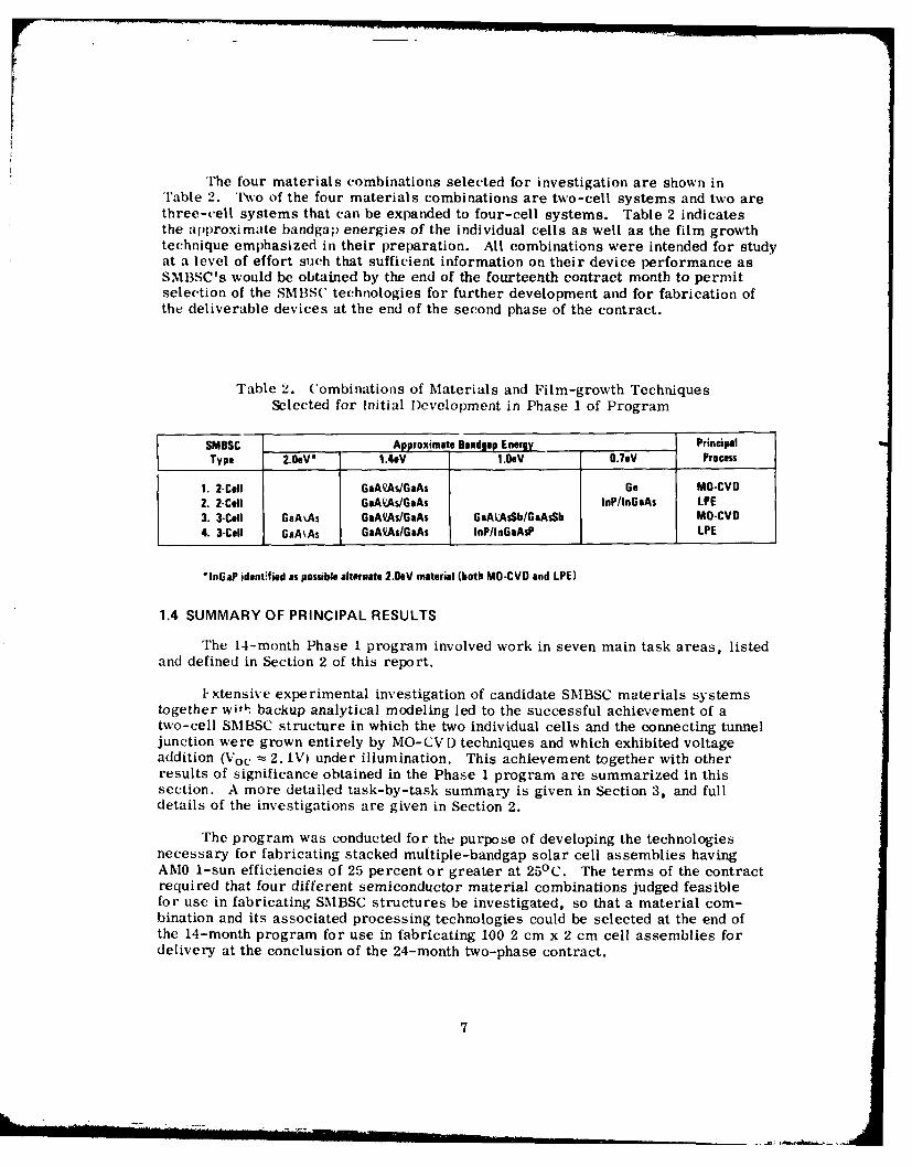
The four materials combinations selected for investigation are shown in'Table 2. Two of the four materials combinations are two-cell systems and two arethree-cell systems that can be expanded to four-cell systems. Table 2 indicatesthe approximate bandgap energies of the individual cells as well as the film growthtechnique emphasized in their preparation. All combinations were intended for studyat a level of effort such that sufficient information on their device performance asSMBSC's would be obtained by the end of the fourteenth contract month to permitselection of the SMIBS" technologies for further development and for fabrication ofthe deliverable devices at the end of the second phase of the contract.
Table 2. Combinations of Materials and Film-growth TechniquesSelected for Initial Development in Phase I of Program
SMBSC Approximate Bandgap Eneray PrincipalType 2.0eV 1.4eV 1.0eV 0.7eV Process
1. 2-Cell GaAIs/GaAs Ge MO-CVD2. 2-Cell GaALAs/GaAs InP/lnGaAs LPE3. 3-Call GaA As GaAMAs/GaAs GaAtAsSb/GaAsSb MO-CVD4. 3-Cell GaAAs GaAlAs/GaAs lnP/InGaAsP LPE
"InGaP identified as possible alternate 2.0eV material (both MO-CVO and LPE)
1.4 SUMMARY OF PRINCIPAL RESULTS
The 14-month Phase I program involved work in seven main task areas, listedand defined in Section 2 of this report.
Extensive experimental investigation of candidate SMBSC materials systemstogether with backup analytical modeling led to the successful achievement of atwo-cell SMBSC structure in which the two individual cells and the connecting tunneljunction were grown entirely by MO-CV Dtechniques and which exhibited voltageaddition (Voc 2. IV) under illumination. This achievement together with otherresults of significance obtained in the Phase 1 program are summarized in thissection. A more detailed task-by-task summary is given in Section 3, and fulldetails of the investigations are given in Section 2.
The program was conducted for the purpose of developing the technologiesnecessary for fabricating stacked multiple-bandgap solar cell assemblies havingAMO 1-sun efficiencies of 25 percent or greater at 25 0 C. The terms of the contractrequired that four different semiconductor material combinations judged feasiblefor use in fabricating SMBSC structures be investigated, so that a material com-bination and its associated processing technologies could be selected at the end ofthe 14-month program for use in fabricating 100 2 cm x 2 cm cell assemblies fordelivery at the conclusion of the 24-month two-phase contract.
7
Accordingly, investigations were undertaken on the following SMBSC materialssystems, all of which involve the GaA2As-GaAs system as the basic buildingblock: 1) the two-cell GaAs-Ge structure, made by MO-CVD and conventional CVDtechniques; 2) the two-cell GaAs-LnGaAs structure, using LPk methods; 3) thethree-cell GaAe As-GaAs-GaAsSb structure, employing MO-CVD methods; and4) the three-cell GaA As-GaAs-InGaAsP structure, involving LPE methods.
After the program was under way, MBE techniques were incorporated into theinvestigations of structures 1, 3, and 4 by mutual agreement of the Air Force andRockwell. Late in the program, with three months of Phase 1 remaining, a changein program emphasis was introduced by the Air Force to limit the investigationsto GaAeAs-GaAs and GaAs-Ge two-cell structures and the possible GaAAs-GaAs-Gethree-cell assembly that might also result. Primary emphasis was to be on theMO-CVD technique, supplemented- when appropriate -by MBE, LPI, or otherdeposition and/or processing methods.
The best results were achieved with the two-cell GaAeAs-GaAs structuremade entirely by MO-CVD, although similar structures made by a combination ofMO-CVD and MBE techniques appeared quite promising. Two-cell GaAs-Geassemblies, made by a combination of MO-CVD and conventional CVD methods orby combined MO-CVD and MBE techniques, were not as successful, althoughtheoretically capable of essentially the same overall efficiency (up to -25 percent)as the GaA2 As-GaAs tandem structure. No attempt was made during the Phase 1program to prepare a three-cell GaAfAs-GaAs-Ge stacked assembly. The othermaterials combinations included in the original program received considerably lessattention during the investigations, and correspondingly less progress toward theprogram goals was made with those structures.
The investigation of the three-cell GaAeAs-GaAs-GaAsSb tandem structurereceived major program emphasis, and within that investigation, the GaAe As-GaAstwo-cell SMBSC was extensively developed. Although exclusively MO-CVD tech-niques were originally expected to be involved, MB methods were also appliedbeginning part way through the program. The principal developments requiredwere satisfactory GaAeAs large-bandgap (1.8-2.0 eV) cells and conducting (pre-sumably tunneling) junctions in GaA2 As and/or GaAs (with the former preferred)to provide the non-rectifying connecting layer between cells of the SMBSC. TheGaAsSb materials system was investigated briefly using LPE techniques (see below),but MO-CVD studies with these materials had not been undertaken prior to the timeat which the program emphasis was changed.
Window-type alloy cell structures were grown by MO-CVD on n+GaAs:Si andn+GaAs:Te substrates with typical configurations pGal.vA YAs/pGal-yApxAs/nGaixAfxAs (y 0.8, x = 0.2-0.4), in some cases with a thin p+Ga.As:Zn caplayer on top to facilitate contacting the p layer of the cell. Deposition temperaturesranged from 700 to 8000C, with 7500C the most common. Most cells were0.5 cm x 0.5 cm, although small mesa cells were processed in some cases.
Cell response appeared to improve generally with increasing deposition tem-perature, and active layer compositions of x = 0.24-0.30 seemed preferable. Thebest cell parameters observed were in a structure grown at -750°C with y = 0.8 and
8
x =0.24: Voc = 0. 96V, Jsc = 12.0 mA/cm 2 , fill factor =0.63, and 7) = 5.4 percent(AMO, no AR coating). Spectral response measurements showed that reducedshort-wavelength response was the cause of the relatively small Jsc values obtained,and it appeared that poor current collection efficiency (i.e., short minority-carrierdiffusion lengths) in the p-type junction layer most likely caused the reducedshort-wavelength response.
Further studies of a variety of alloy cell configurations indicated that,although Voc increased as the AR content of the junction layer increased, the Vocvalues were always appreciably less than theoretically expected values except forvery low Ae content (x < 0. 10); highest Voc values found were -1. 1V for cellswith x = 0.35. The Jsc values were found to depend on Ae content and thicknessof the window layer as well as the junction layers. Junction depths < 0.7 ±m wereclearly preferred, with thicker layers causing reductions in Jsc - consistent withminority-carrier diffusion lengths ! 0.5 jm. Window layer compositions withy = 0.9 allowed better blue response and higher Jsc values than those with y = 0. 8,and window layer thicknesses ! 800A were preferred.
Most cells had Jsc values < 6 mA/cm 2 (AM0, no AR coating) irrespective ofdesign; fill factors typically ranged from 0.60 to 0.76 and efficiencies were generally! 4 percent (AMO, no AR coating). Thus, as of the end of the Phase 1 program theperformance of the GaA2As cells still requires considerable improvement, socontinued emphasis is expected in Phase 2.
Several attempts were made to achieve tunneling properties in GaAd As junctionstructures grown by MO-CVD, beginning early in the program. Both n+/p + andp+/n + junction structures with Gal.yAi As compositions of y = 0.08 to y = 0.37were grown at temperatures of 700 and 750°C, but at best only weak tunneling wasobserved. Although the emphasis in the remainder of Phase 1 was on tunnel junc-tion structures in GaAs (see below), it is expected that further effort will bedevoted to achieving tunneling structures in the alloy in the Phase 2 program sincethat configuration is preferred in terms of overall performance of the stackedassemblies.
Good tunnel-junction intercell connecting structures were made in GaAs byboth MO-CVD and MBE techniques. Both n+/p + and p+/n + structures were madeby MO-CVD at temperatures from 630 to 7500 C, with better results obtained at- 6500C, as shown in Figure 3. Very high (essentially ohmic) junction conductivitywas achieved in some of the structures - especially in n+/p+ structures - more thanadequate for use as an intercell connection under 1-sun AMO conditions. Preliminaryannealing tests indicated that the tunneling characteristics might not survive subse-quent elevated temperature processing required for growth of the top cell in astacked assembly because of diffusion of the Zn dopant in the p+GaAs, but n+/p +
structures grown in GaAs at 6300C were used in the first successful two-cellGaAe As-GaAs SMBSC described below. However, the still-open question aboutthe consistent stability of these structures at high temperatures requires furtherinvestigation in the Phase 2 program.
9
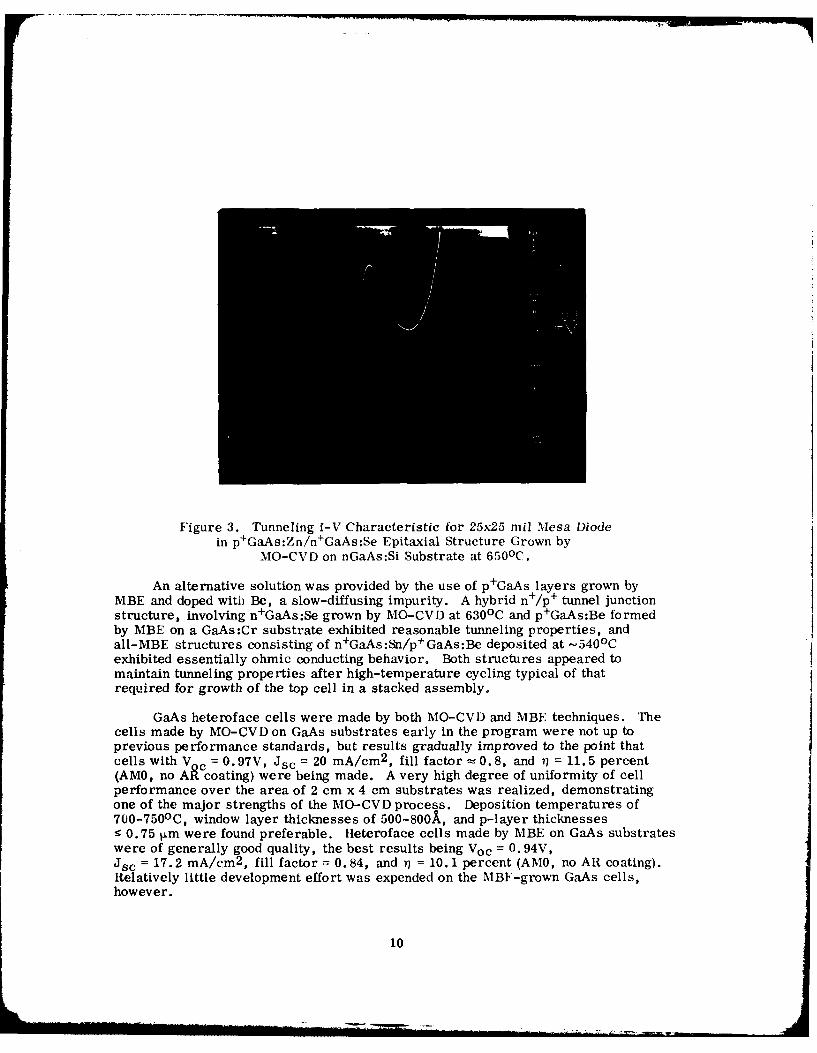
Figure 3. Tunneling I-V Characteristic for 25x25 mil Mesa Diodein p+GaAs:Zn/n+GaAs:Se Epitaxial Structure Grown by
MO-CVD on nGaAs:Si Substrate at 6500 C.
An alternative solution was provided by the use of p+GaAs layers grown byMBE and doped witil Be, a slow-diffusing impurity. A hybrid n+/p + tunnel junctionstructure, involving n+GaAs:Se grown by MO-CVD at 630 0 C and p+GaAs:Be formedby MBE on a GaAs:Cr substrate exhibited reasonable tunneling properties, andall-MBE structures consisting of n+GaAs:Sn/p + GaAs:Be deposited at -540 0 Cexhibited essentially ohmic conducting behavior. Both structures appeared tomaintain tunneling properties after high-temperature cycling typical of thatrequired for growth of the top cell in a stacked assembly.
GaAs heteroface cells were made by both MO-CVD and MBE techniques. Thecells made by MO-CVD on GaAs substrates early in the program were not up toprevious performance standards, but results gradually improved to the point thatcells with V = 0. 97V, Jsc = 20 mA/cm 2 , fill factor - 0.8, and n = 11,5 percent(AMO, no Al ccoating) were being made. A very high degree of uniformity of cellperformance over the area of 2 cm x 4 cm substrates was realized, demonstratingone of the major strengths of the MO-CVD process. Deposition temperatures of700-7500 C, window layer thicknesses of 500-80,X, and p-layer thicknesses9 0.75 tm were found preferable. Ileteroface cells made by MBE on GaAs substrateswere of generally good quality, the best results being Voc = 0. 94V,Jsc = 17.2 mA/cm 2 , fill factor = 0.84, and 77 = 10. 1 percent (AMO, no AR coating).Relatively little development effort was expended on the MBF-grown GaAs cells,however.
10
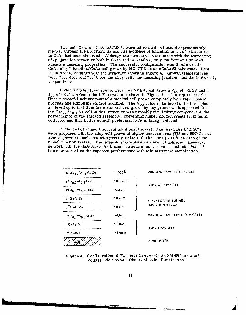
Two-cell GaA As-GaAs SMBSC's were fabricated and tested approximatelymidway through the program, as soon as evidence of tunneling in nf/p+ structuresin GaAs had been observed. Although the structures were made with the connectingn+/p + junction structure both in GaAs and in GaA As, only the former exhibitedadequate tunneling properties. The successful configuration was GaA As cell/GaAs n+-p + junction/GaAs cell grown by MO-CVD on an nGaAs:Si substrate. Bestresults were obtained with the structure shown in Figure 4. Growth temperatureswere 750, 630, and 7000 C for the alloy cell, the tunneling junction, and the GaAs cell,respectively.
Under tungsten lamp illumination this SMBSC exhibited a Voc of -2. 1V and aJsc of -4.5 mA/cm 2 ; the I-V curves are shown in Figure 5. This represents thefirst successful achievement of a stacked cell grown completely by a vapor-phaseprocess and exhibiting voltage addition. The Voc value is believed to be the highestachieved up to that time for a stacked cell grown by any process. It appeared thatthe Ga0. 7 A 0 3 As cell in this structure was probably the limiting component in theperformance of the stacked assembly, preventing higher photocurrents from beingcollected and thus better overall performance from being achieved.
At the end of Phase 1 several additional two-cell Gake As-GaAs SMBSC'swere prepared with the alloy cell grown at higher temperatures (775 and 800°C) andothers grown at 7500C but with greatly reduced thicknesses (~100A) in each of thetunnel junction layers. The intended improvements were not achieved, however,so work with the GaA2 As-GaAs tandem structure must be continued into Phase 2in order to realize the expected performance with this materials combination.
p+Ga 0 .2 A 0.8 As:Zn -1000, WINDOW LAYER (TOP CELLI
pGa 0 7 Ak0 3 As:Zn 0.75pm A"_____ "______1.8EY ALLOY CELL
nGa 0 .7 A 0.3 As:Se -2.51m
n+GaAs:Se -'04pm I CONNECTING TUNNEL
p+GaAs:Zn -0.4im J JUNCTION IN GaAs
pGa 0 .7 Ak 0 3As:Zn -'0.51im WINDOW LAYER (BOTTOM CELL)
pGaAs:Zn -l.0,m_1.4eV GaAs CELL
nGaAs:Se -4.0pm
/////x .SUBSTRATE
Figure 4. Configuration of Two-cell GaA2As-GaAs SMBSC for whichVoltage Addition was Observed under Illumination
1I
L9
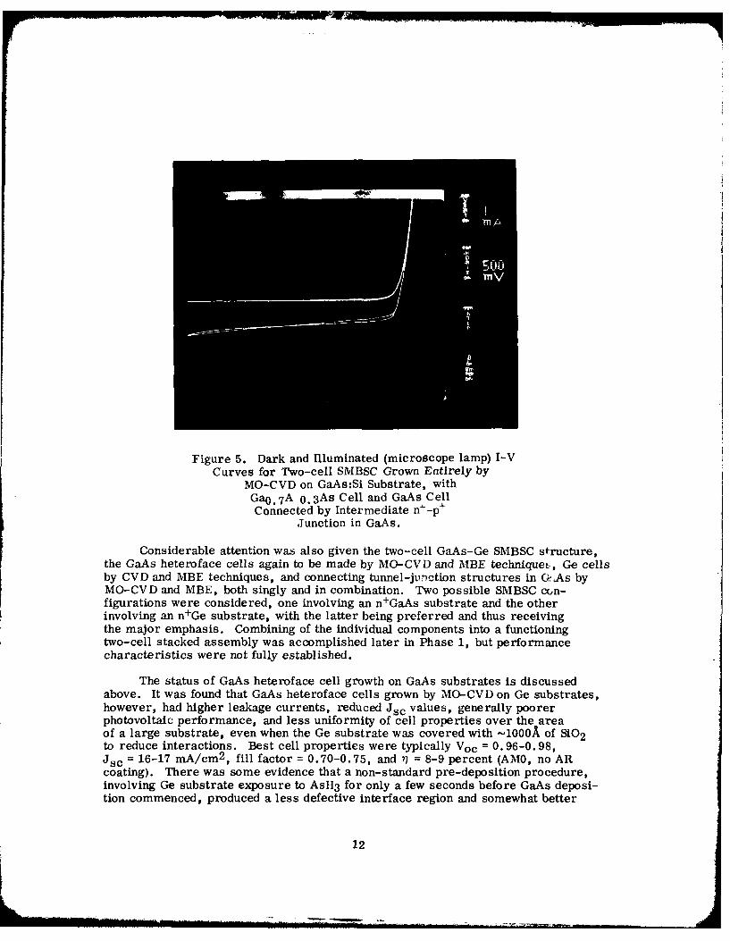
Figure 5. Dark and Illuminated (microscope lamp) I-VCurves for Two-cell SMBSC Grown Entirely by
MO-CVD on GaAs:Si Substrate, withGa 0 . 7 A 0 .3As Cell and GaAs CellConnected by Intermediate n+-p +
Junction in GaAs.
Considerable attention was also given the two-cell GaAs-Ge SMBSC structure,the GaAs heteroface cells again to be made by MO-CVD and MBE techniques, Ge cellsby CVD and MBE techniques, and connecting tunnel-junction structures in G.As byMO-CVD and MBE, both singly and in combination. Two possible SMBSC cun-figurations were considered, one involving an n+GaAs substrate and the otherinvolving an n+Ge substrate, with the latter being preferred and thus receivingthe major emphasis. Combining of the individual components into a functioningtwo-cell stacked assembly was accomplished later in Phase 1, but performancecharacteristics were not fully established.
The status of GaAs heteroface cell growth on GaAs substrates is discussedabove. It was found that GaAs heteroface cells grown by MO-CVD on Ge substrates,however, had higher leakage currents, reduced Jsc values, generally poorerphotovoltaic performance, and less uniformity of cell properties over the areaof a large substrate, even when the Ge substrate was covered with -1000A of SiO2to reduce interactions. Best cell properties were typically Voc = 0.96-0.98,Jsc = 16-17 mA/cm 2 , fill factor = 0.70-0.75, and 77 = 8-9 percent (AMO, no ARcoating). There was some evidence that a non-standard pre-deposition procedure,involving Ge substrate exposure to AsH3 for only a few seconds before GaAs deposi-tion commenced, produced a less defective interface region and somewhat better
12
cell performance. Modifications in cell layer dimensions and doping impurityconcentrations and improved Ge substrate quality are expected to result in con-siderably better GaAs cell performance in future work with this materialcombination.
In addition to the heteroface GaAs cells grown by MBE on GaAs substrates(mentioned above), junction structures were also grown on Ge substrates by thistechnique. Although the layers were of high quality it appeared that heterojunctionshad also been formed, unintentionally, at the GaAs-Ge interface. Since relativelylittle effort was devoted to MBE-grown GaAs cells on either GaAs or Ge substratesin Phase 1, the work is expected to be expanded in the Phase 2 program.
Ge solar cells were made by both CVD (GeH4 pyrolysis in H2 ) and MBE tech-niques; some limited investigations were also conducted with spin-on oxide impuritysources for producing diffused junction structures. Most of the cells were preparedon Ge substrates, that being the preferred configuration for the SMBSC. Best CVDquality was obtained at the upper end of the useful deposition temperature range(-8000 C) and with relatively high deposition rates (-0. 7 km/min). However,substrate stability can become a problem during long depositions at such tempera-tures. The best CVD cell parameters, obtained with B-doped p layers and undopedn-type layers on nGe substrates, were Voc = 190-200 mV, Jsc = 31-33 mA/cm 2 ,fill factor = 0.65, and 77 = -3 percent (AMO, no AR coating). Much improvedresults are expected with changes in cell layer thicknesses and doping concentrations(especially the n layers) and in the cell contacting procedures; these changes areplanned for the Phase 2 program.
Ge cell structures were also made by MBE techniques, by depositing a layerof As on p-type (100)Ge and subsequently diffusing the As into the Ge in situ atappropriate temperatures. The resulting diffused-junction cells were not as goodas those made by CVD but were adequate for use in preparing experimental stackedGaAs-Ge SMBSC structures using exclusively MBE techniques.
Experimental two-cell GaAs-Ge stacked assemblies were made entirely byMBE techniques and by combined MO-CVD and MBE, late in the program. Theall-MBE structure appeared to contain a double heterojunction rather than theintended structure; the hybrid structure, which involved an MO-CVD heterofaceGaAs cell grown at 750 0 C on an n+/p + GaAs tunnel junction structure grown byMO-CVD at 630 0 C on a diffused Ge cell structure formed by MBE techniques, wasnot fully processed and evaluated prior to the end of the program. It is expectedthat additional GaAs-Ge SMBSC's prepared by various combinations of CVD andMBE techniques will be investigated in Phase 2.
Investigation of the two-cell GaAs-InGaAs SMBSC, to be prepared by LPEmethods on n+GaAs substrates, involved mainly the experimental growth ofinP layers on GaAs substrates (to provide the lattice-matched window for theInGaAs cell) and of InGaAs layers on InP, in addition to an evaluation ofA2GaAsSb as an alternative materials system to nGaAs for the low-bandgap cell.
The LPE growth of p+InP layers on n+GaAs substrates from both In and Sn sol-vents was only partially successful. Acceptable growth on (111B)GaAs was achievedwith In solvent in a narrow temperature range around 520 0 C, and marginally
13
6
acceptable growth on (100)GaAs was obtained with Sn solvent at higher temperaturesprovided that large vertical temperature gradients were maintained across theliquid-solid growth interface to minimize etch-back. However, high densitiesof inclusions persisted at the interface, so these structures were not satisfactoryfor stacked cell configurations. Consequently, InP layers grown on GaAs substratesby MO-CVD were separately prepared for the subsequent LPF growth experimentswith InGaAs.
Initial LPE growth experiments with the InGaAs composition lattice-matchedto InP were done with single-crystal (111B)InP substrates. Junction structures ofpInGaAs:Zn/nnGaAs (undoped) were grown, and despite some problems in makingohmic contacts cell structures were fabricated and characterized; low currentcollection efficiency, junction movement due to Zn diffusion, and possible formationof an InP-InGaAs heterojunction resulted in generally poor performance. Whenthicker undoped single layers were grown at lower temperatures (-630()C), withslight substrate etchback allowed prior to growth, an n-type layer of compositionI.nO.5 3 GaO. 4 7 As (Eg - 0.7 eV) resulted and a junction was formed in it by Znout-diffusion from the p+ substrate.
Solar cells exhibited Voc values <0. IV and Jsc values of -16 mA/cm 2 (AMi,no AR coating). The low Voc values were attributed to large reverse saturationcurrents and poor diode factors, and there was again some indication of a possibleheterojunction at the nP-InGaAs interface. Subsequent preliminary experimentswith the MO-CVD InP/GaAs composite substrates resulted in discontinuous layersand poor melt wipeoff, but the experiments were not continued because of thechange in program emphasis that became effective at that time.
Some attention was also given to Ae GaAsSb as an alternative small-bandgapcell material. Window-type cell structures were grown on n-type single-crystalGaSb substrates by LPE with the configuration pGa0 7 A2 0 3 AsSb/pGaSb (undoped)/nGaSb (substrate), but poor photovoltaic properties (especially fill factor andshort-wavelength response) were obtained. Modified structures, with improvedcontacts to reduce series resistance and thinner pGaSb layers to improve short-wavelength response, were then prepared with the configuration p+GaO. 7A0. 3 AsSb/pGa0 9 A2 0 1 Sb/nGaSb (substrate). Addition of AS to the GaSb p layer reduced thelayer growih rate, so that shorter deposition times (I min at -520 0 C) permittedgrowth of p layers that were 2-3 m thick.
These changes allowed attainment of cells with the parameters Voc = 0. 240V,Jsc = 29 mA/cm 2 , fill factor = 0.51, and q 3.5 percent (AM1, no AR coating).Junction leakage and series resistance remained as problems, but the results weresufficiently encouraging to prompt a brief investigation of various contact materialsfor both p-type and n-type GaSb to attempt to reduce series resistances losses.Pure Au contacts were found best for both conductivity types. Several additionalcell structures, including some with higher A2 composition (~0. 7) in the windowlayer, were subsequently prepared, but the investigations were not carried further.
The study of the three-cell LPE-grown GaA2As-GaAs-InGaAsP SMBSC assem-bly using n+GaAs single-crystal substrates involved two main areas of investigation -LPE growth of 2.0 eV GaA As cell structures on GaAs surfaces and LPE growth
14
of 1.0 eV InGaAsP layers. Existing well-established methods for LPE growthof GaAs cells provided the third major cell technology needed for this SMBSC. TheGaAs (or GaA2 As) tunnel junctions and InP/GaAs tunneling heterojunctions made byeither LPE or MBE techniques would provide the needed cell interconnections.
Window-type alloy cell structures were grown by LPE on n+GaAs substrateswith the configuration p+Ga0. 1 Ae o. 9 As/pGa0 . 7A&0
. 3As/nGa0. 7 A20 . 3 As. Someexperimental n+/p+ alloy structures were also grown, but incomplete wipeoff in theLPE boat resulted in cross-contamination of the melts and unsatisfactory structures.A special LPE boat was then designed, and fabrication was completed by an outsidevendor several months later. Modified LPE growth procedures were developedfor use with the new boat, and several types of alloy cell structures were prepared.
Complete small-area window-type cells were fabricated both by conventionalprocessing and by processing that involved Zn diffusion into the window layer.Window-layer AR contents were in the range y = 0.8-0.9 and junction layer A2contents x = 0.2-0.4. The cells generally had good fill factors (typically 0.7-0.8)but relatively low Voc and Jsc values. Spectral response curves showed poorutilization of the short-wavelength illumination, indicating needed changes in windowlayer thickness and junction layer thickness and Ae content.
Some additional alloy cells were prepared near the end of Phase 1, includingseveral in which only a p-type active layer and a p-type window layer were depositedin succession by LPE on an n+GaAs substrate, followed by Zn diffusion through thewindow layer and the p layer to produce the active p-n junction just inside thesubstrate. However, it was found difficult to control the diffused junction depth.The cells grown and processed by conventional procedures were somewhat better;Jsc values up to 8.5 mA/cm 2 and efficiencies up to 4.6 percent (AMO, no AR coating)were obtained. Open-circuit voltages (-1.0V) and fill factors (-0.75) were aboutthe same for both types of cell.
Limited investigation of the LPE growth of InGaAsP for the 1.0 eV bandgapcell was also undertaken. Multilayer structures of the configuration pinP/pInGaAsP/nInGaAsP/nInP were grown on n+InP substrates. Analysis showedthe quaternary layers had the composition In0 . 7 5 Ga 0 . 2 5 As 0 . 5 PO. 5, indicatinga bandgap of -1 eV and a lattice match to InP, but photoresponse measurementsshowed cutoff at the InP band edge. This was believed caused by Zn dopant diffusionfrom the two upper layers into the nInP buffer layer, shifting the active junctionto that location. The study of this quaternary was not carried further in Phase 1.
Cell modeling and analysis studies in the Phase 1 program showed that onlylimited response is achievable for a Ge cell in the wavelength region beyond thedirect bandgap (X > 1.5 pLm), even for a thick wafer-based cell, but that use of aback-surface field considerably enhances the response of a thin (i. e., all depositedfilm) cell in the region 0.9 ! X t 1.5 pLm.
The studies also led to estimates of - 0.5 ptm for the minority-carrier diffusionlengths in the p-type junction layers of heteroface GaAfAs alloy cells, throughcomparison of modeled spectral photoresponse with experimentally determined
15
"Nia
responses of MO-CVD and LPE cell structures. Similar matching of modeled andmeasured spectral photoresponses for thin-window GaAs cells, especially thosemade by MBE techniques, was undertaken and led to the conclusion that specificreflectivity measurements must be made for GaAs cells having GaAl As windowlayers if correct internal photoresponse curves are to be obtained.
Analytical techniques were also applied to the development of an algorithmthat provides the design parameters for n-layer (n 2 3) antireflection coatings foruse on SMBSC assemblies, which have spectral ranges broader than those of anyof the component cells involved. Three-layer coating designs for two-, three-,and four-cell assemblies were developed using MgF 2 or CaF 2 for the top layer,SiO2 for the middle layer, and Ta 2 0 5 or TiO2 for the bottom layer. No experi-mental development of the coatings was undertaken in Phase 1, however.
16

2. DETAILED DISCUSSION OF RESULTS
This section contains detailed descriptions of the technical activities and theresults achieved during the 14-month Phase 1 program. The discussion is arrangedin order by technical task, with one exception noted below.
Pursuit of the Phase 1 program objectives specified in Section 1. 2 was accom-pli shed by means of seven main technical tasks, as follows:
1. SMBSC Modeling and Analysis
2. GaAs-Ge SMBSC Technology Development
3. GaAs-[nGaAs SMBSC Technology Development
4. GaAIAs (2. OeV)-GaAs-GaAsSb SMBSC Technology Development
5. GaAfAs (2.OeV)-GaAs-lnGaAsP SMBSC Technology Development
6. Characterization of Materials and Photovoltaic Devices
7. Development of AR Coating Technology.
The work of the first six tasks was planned to begin in the first morith of the contract;the activity of Taqk 7 was scheduled to commence in the seventh month of the pro-gram.
Task 1 and Task 7 were carried out primarily at the Rockwell Thousand Oakslaboratories. Tasks 3 and 5 were planned to involve application of LPE techniquesand thus were also pursued at the Thousand Oaks facility.
Tasks 2 and 4 involved use of the MO-CVD technique and thus were centered atthe Anaheim laboratories of the Rockwell Electronics Research Center. The mate-rials and device characterization work of Task 6 was carried out at both laboratoriesthroughout the Phase 1 program.
Following a contract program progress review meeting held at the end of theeleventh month of the contract a change in program emphasis was agreed upon forthe remaining three months of Phase 1. Experimental results achieved in the pro-gram up to that time, as well as related experimental results being achieved inother programs at Rockwell at the same time, prompted the following modifiedapproach for Phase 1:
1. The program effort was to be limited to GaAlAs-GaAs, GaAs-Ge, andGaAfAs-GaAs-Ge stacked multiple-bandgap solar cell systems.
2. There was to be greatly increased emphasis on the MO-CVD techniquefor making these structures.
17
3. Other deposition and processing techniques were to be used in certainhybrid combinations to augment CVD when it appeared that doing so wouldimprove the chances of achieving the program goals; those other techniquesmight include LPE, molecular beam epitaxy (MBE), thermal diffusion, orion implantation.
Thus, effective at the start of the twelfth month of the Phase 1 program thecontract work emphasized only the GaAfAs-GaAs-Ge materials system and thetwo-cell and three-cell stacked assemblies that can be made in that system. Theemphasis was on use of ('VD techniques, especially M t)-('VD, although other growthand processing methods (L3E, MBE) were utilized to supplement the CVI) methods.
The activities and the results associated with these tasks are described in thefollowing discussions, arranged by task except for the work of Task 6 (Characteriza-tion of Materials and Photovoltaic Devices), which is included as appropriate inthe other task discussions.
2.1 SMBSC MODELING AND ANALYSIS
Because of the complexity of SM BSC structures and the fact that there waslittle experimental information prior to the start of this program on the behaviorof individual solar cells used in monolithic tandem assemblies, it was veryimportant to provide some guidance for the experimental investigations by meansof analytical modeling of the structures involved.
Considerable previous work had been done at Rockwell on the modeling ofGaAs solar cell performance both for normal one-sun illumination intensities andfor high -concentration (multiple-sun) illumination conditions. Those analysesutilized theoretical expressions that were strengthened with actual cell performanceparameters obtained with a variety of experimental cell structures.
The requirement that the individual cells connected in tandem in the SMBSCstructure must share a common current -that is, that the photogenerated currentof each cell at its operating point when used in the stacked assembly must matchthat of every other cell in the SMBSC -places very stringent limitations on thecomposition, the design, and the photovoltaic properties of these cells. Thismakes it essential to understand and control the properties of the individual cellsin detail. Accurate analytical modeling of both individual and stacked cell per-formance can assist in achieving this needed understanding and control, and canoften prevent the conduct of unnecessary or superficial experiments and provideguidance to the really essential ones.
Similarly, the AR coating requirements of a tandem cell assembly will bedifferent from those of, for example, the uppermost cell in the stack if it wereused individually in its more restricted spectral range. Analytical modeling canprovide the data required to develop a satisfactory broad-band AR coating forSMBSC structures of various configurations.
Thus, this task was to include the generation of refinements in the existingmodel used at Rockwell for solar cell performance analysis, incorporating experi-mental data on the I-V characteristics of various photovoltaic junctions as well asnonrectifying junctions. Application of the improved model was expected to lead
18
to identification of candidate two-cell, three-cell, and four-cell SMBSC combinationspotentially useful and feasible for experimental studies. Calculations were alsoto be made for the purpose of determining optimum materials properties, such asdoping levels and alloy compositions, and optimum physical design parameters,such as electrical contacts and AR coatings, for the candidate SMBSC systems ofinterest. The results of the modeling calculations were expected to stronglyinfluence the experimental program; it was intended that considerable mutualinteraction between this task and the experimental investigations would occur,particularly during the first six months of the program.
2. 1. 1 Multilayer AR Coating Design
One of the first problems to be examined in this task was that of AR coatingdesigns for SMBSC assemblies. Although the development of suitable AR coatingtechnologies would be done under Task 7 (Section 2. 6) the necessary modeling andanalysis for such development is part of this task.
The SMBSC structure requires the suppression of reflection from the surfaceover a broad spectral range. The number of dielectric layers required and theircomposition and thickness will depend on the cell material in the top layer and thespectral bandwidth to be covered. For a two-cell system with GaAs as the top layerthe spectral bandwidth is 0. 3-1. 8pm. For a three-cell system with GaAfAs or GaInPas the top cell material the spectral bandwidth is 0.3-1. 2pm, and for a four-cellsystem with GaAfAs or GaInP as the top cell material the bandwidth is again 0.3-1. Spr
Because of the different optical reflectivity vs wavelength characteristicsfor a given thin-film material when used in a stacked multilayer assembly relativeto its characteristics when used alone or on a substrate of identical composition itwas necessary to reevaluate the requirements for AR coatings for the materialsused in the SMBSC structures being developed in this program. Consequently,preliminary consideration was given to those requirements by means of modelinganalysis of a two-layer AR coating for a GaAs surface over the broader wavelengthband of importance for a SMBSC, namely, the range from -0. 3pm to -1. 8pm.
Attempts to extend the wavelength range of coverage of the existing two-layeralgorithm suggested that the covered spectral band could probably be expanded tothe interval 0.5-1. 7pm wavelengths with less than 10 percent reflection at any onewavelength and about 6 percent average loss throughout the band, with a high-reflectivity (-13 percent) peak near the center of the band (at -1. 15 m). However,the reflection loss outside this band was found to be considerably higher, with anespecially steep increase in the reflectivity at the short-wavelength end of the band.The preliminary calculations indicated that three or more layers would probablyovercome this problem, so attention was directed to development of an algorithm fora multilayer AR coating of n layers, with n 3.
The resulting algorithm can be used with a given set of constraints to optimizethe values of independent variables using a generalized technique (Ref 7). In thisprogram it was used to optimize a three-layer AR coating design. The materialsconsidered for the three layers were restricted to those commonly used for ARcoatings and readily handled experimentally - MgF 2 or CaF2 for the top layer,SiO2 for the middle layer, and Ta2O5 or TiC 2 for the bottom layer (next to thesolar cell).
19
Figure 6 shows the calculated reflection loss as a function of wavelengthfor a three-layer design optimized for 0.3 to 1. 1im operation (three-cell system).The average reflection loss for this case comes out to be 3. 6 percent. Figure 7shows a simular result for 0. 3 to 1. 8 pm operation (two- or four-cell system). Inthis case, the average reflection loss comes out to be 5. 4 percent. In both instancesthe optimization was for minimum integrated reflection loss over the specifiedspectral band.
In practice, however, it is necessary to optimize the short-circuit current or,more accurately, the current at maximum power of the cell assembly. Thisdepends on the solar spectrum and the internal collection efficiencies of the solarcells. When a simplified model for the cell collection efficiency was used withthe AMO spectral distribution, the optimized AR-coating design for the 0. 3 to1. 8pAm range (i.e., for two or four cells in the stack) came out as shown inFigure 8. The overall reflection loss in this case reduces the short-circuitcurrent of the cell assembly by only 3. 8 percent. It should be noted that the peakreflection loss in Figure 8 occurs near 0. 4 m wavelength, while that in Figure 7is at -0. 7pm, so the design of Figure 8 is a better match to the AMO spectrum.
These results demonstrate the power of the algorithm developed for obtainingoptimum AR coating designs. Final design calculations can be performed when-ever the other pertinent experimental data on individual cell performances becomeavailable later in the program.
2. 1.2 Ge Solar Cells
Early in the program some preliminary calculations were carried out for Gesolar cells to assist in determination of the required device parameters for the0. 7eV cell to be used in the two-cell GaAs-Ge SMBSC to be made by MO-CVDin Task 2.
The computer-plotted data of Figure 9 show calculated internal spectralresponse curves for Ge p-n junction cells with (solid curve A) and without (solidcurve B) a back-surface field (BSF) created by the presence of an n+-n junctionat the back of the wafer-based cell structure. The specific device parametersused in the calculations were as follows, with t = thickness, L = minority carrierdiffusion length, and s = surface recombination velocity:
Cell configuration (all Ge): p++/p+/n/n +
Characteristics ofindividual regions: p++ t = 500 -A, Ln = 5pm, s = 106 cm/sec
p t = 1pm, Ln = 50pm, s i = 104 cm/sec
n t = 300Pm
Substrate Lp = 100 m, sb = 100 cm/sec for BSFcase and 105 cm/sec for ohmiccontact case
20
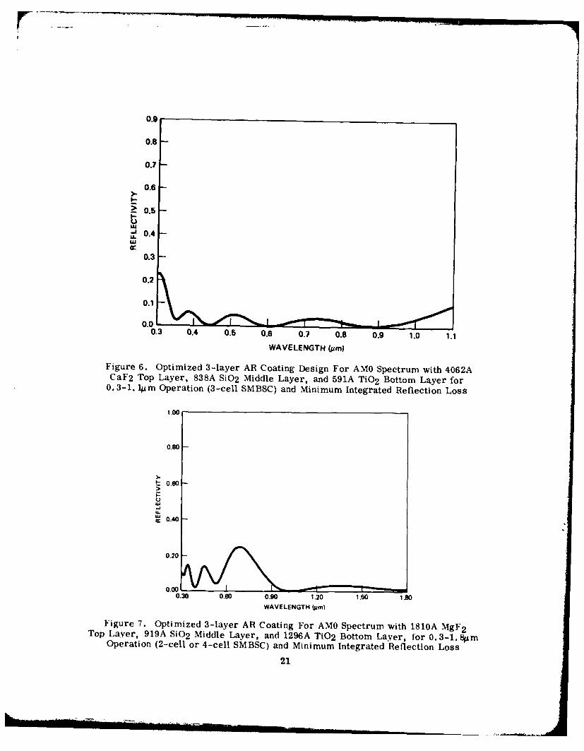
0.9
0.8
0.7
0.6I,-
>0.5
. 0.4U.
0.3
0.2
0.1
0.00.3 0.4 0.5 0.6 0.7 0.8 0.9 1.0 1.1
WAVELENGTH (mm)
Figure 6. Optimized 3-layer AR Coating Design For AMO Spectrum with 4062ACaF2 Top Layer, 838A SiO2 Middle Layer, and 591A TiO2 Bottom Layer for
0. 3-1. lp m Operation (3-cell SMBSC) and Minimum Integrated Reflection Loss
1.00
0.80
S0.60
U
c 0.40
0.20 -
0.000.30 0.60 0.90 1.20 1.60 1.80
WAVELENGTH (pm)
Figure 7. Optimized 3-layer AR Coating For AMO Spectrum with 1810A MgF 2Top LaYer, 919A Si0 2 Middle Layer, and 1296A TiO2 Bottom Layer, for 0.3-1.8 .mOperation (2-cell or 4-cell SMBSC) and Minimum Integrated Reflection Loss
21
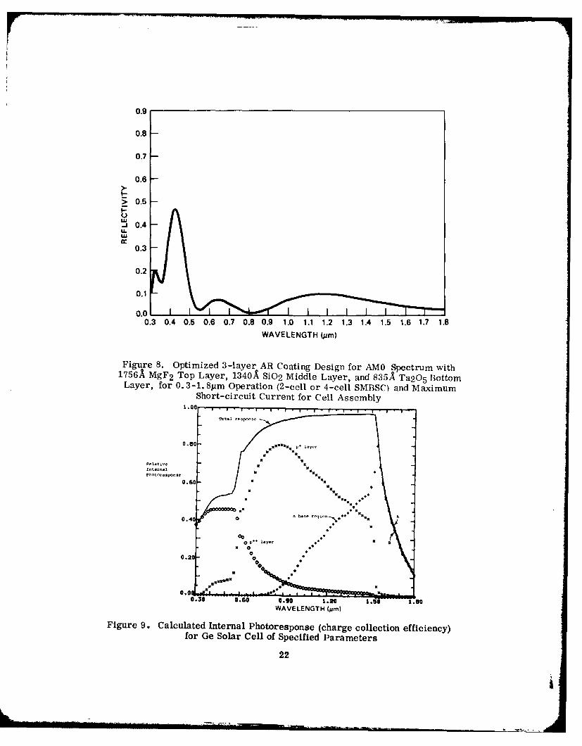
0.9
0.8 -
0.7-
0.6"-
I-
> 0.5-I-
-J 0.4U.
0.3
0.2
0.1
0.0 10.3 0.4 0.5 0.6 0.7 0.8 0.9 1.0 1.1 1.2 1.3 1.4 1.5 1.6 1.7 1.8
WAVELENGTH (pum)
Figure 8. Optimized 3-layer AR Coating Design for AMO Spectrum with1756A MgF 2 Top Layer, 1340A SiO2 Middle Layer, and 835A Ta20 5 BottomLayer, for 0. 3-1. 8 gm Operation (2 -cell or 4-cell SMBSC) and Maximum
Short-circuit Current for Cell Assembly
Internal respon
Photorespon~e izl•
0.60U.
xU %
0.40 reqAon..\*A* Us
0 p+- layer
0.20 - 0**
o .
O.30 0.60 C." 1.20 1.50 1.80
WAVELENGTH (urn)
Figure 9. Calculated Internal Photoresponse (charge collection efficiency)for Ge Solar Cell of Specified Parameters
22
I
The calculated spectral response data for the individual layers of this cell
structure are also shown in the figure as plotted data points. It can be seen that even
with a base region (substrate wafer) that is :0pm thick the cell response for energies
below the Ge di rect bandgap (wavelengths greater than ~1.5pm) decreases quite rapidly.
Furthermore, the back-surface field does not incream the long-waveleng-th response
very much because of the very limited optical absorption in the region of the indirect
bandgoap. To collect photocurrent efficiently at wavelengths beyond 1. 5pm and up to
about 1.,,pm (corresponding to the indirect bandgap of Ge) very thick Ge substrates
would be required, and not much help would be obtained from the back-surface field.
However, such a back-surface field can be used to advantage to enhance photocurrent
collection in very thin Ge cells in the region out to the direct-gap wavelength of
1. 5pm. This would be a significant improvement for a thin Ge cell made by an
epitaxial growth process on, for example, a GaAs substrate wafer. (See Section 2. 2.)
The calculated spectral response curves for a thin epitaxial Ge cell (-(pr
thickness) with and without the back-surface field from an n-n- back junction are
shown in Figure 10. The device parameters used in these calculations were as
follows:
Cell config-uration p ++/p+/n
(p+'/p+/n/n + with back junction)++ =5ms = 16 c/e
p region: t = 500A, L n 5pm, s 10 cm/sec+ = as = 14 c/e
p region: t = 1pm, Ln 50/m, s 10 cm/sec
n region: t 5pm, L= 100pm, s = 105 cm/sec for ohmic contact casep
= 100 cm/sec for BSF case
A distinct improvement in spectral response between 0.9 and 1. 5pm is seen to result
from the presence of the back-surface field, which was assumed for this calculation to
result in a surface recombination velocity at the back surface of 100 cm/sec. The
back-surface recombination velocity can be related to the device parameters through
the following expression:
D pn+Nn c ns nn- pn+Nn+ L n+
where Sn+ is the n-n+ interface recombination velocity, Dpn+ is the diffusion constant
for holes in the n+ region, Nn is the electron concentration in the n region, Lpn+ is
the hole diffusion length in the n+ region, Nn+ is the electron concentration in the n+
region, and wn+ is the thickness of the n+ region. From this expression suitabledevice parameters can be selected to result in a value of 100 cm/sec for the surface
recombination velocity.
An epitaxial Ge cell of such dimensions could be used as part of the two-cell
GaAs-Ge SMBSC configuration being developed in Task 2. The accuracy of the Ge
cell model can be further improved when experimental data on Ge cells fabricatedin the Task 2 effort become available and are incorporated into the model.
23
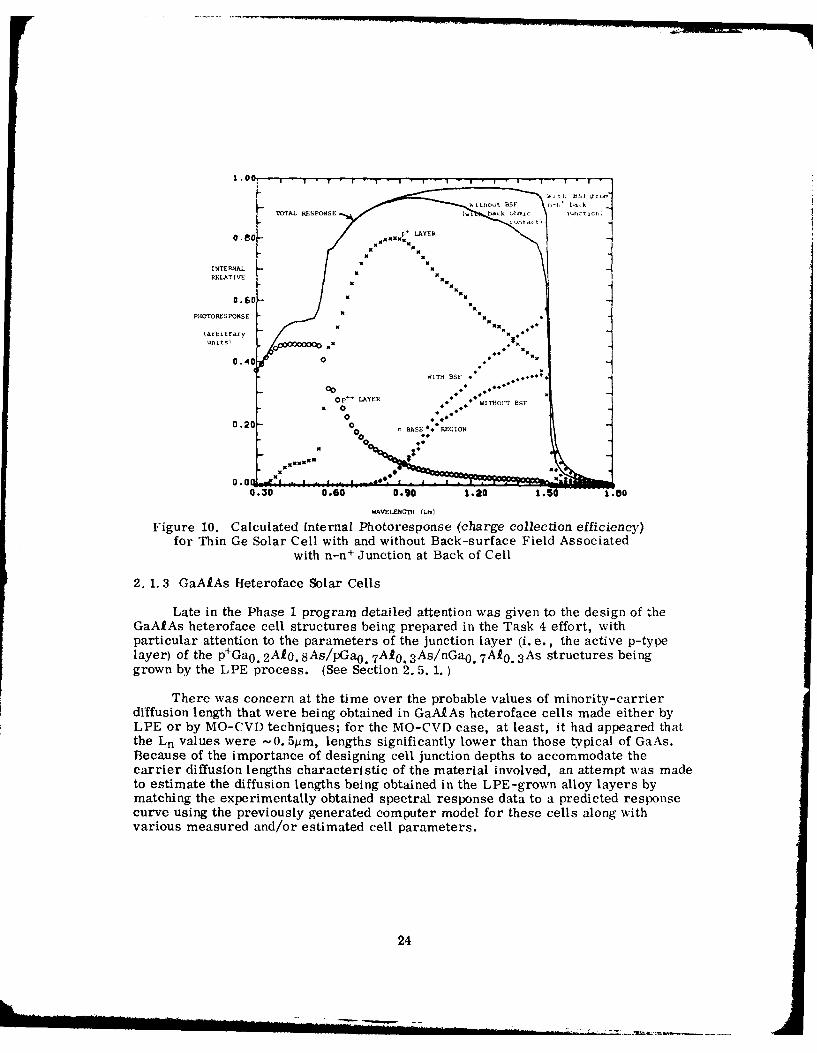
1 .00; t
I ' I '
-- itout B5 t.f* kT OTAL RESPONSE (S back o5hi (Urt, toof
INTERNAL
LELATIYVE
PTORSRESSPONSE W %
(arbitrary x
0.4K 0
0 oLL0 n A S E K . R E G IO N
0.30 0.60 o. o .20o .. 0 1.80WAVELENGTH (Sm)
Figure 10. Calculated Internal Photoresponse (charge collection efficiency)for Thin Ge Solar Cell with and without Back-surface Field Associated
with n-ni Junction at Back of Cell
2, 1. 3 GaAIAs Heteroface Solar Cells
Late in the Phase 1 program detailed attention was given to the design of theGaAMAs heteroface cell structures being prepared in the Task 4 effort, withparticular attention to the parameters of the junction layer (i. e., the active p-typelayer) of the p GO 2 A20.8As/pGao 7 A10 3 As/nGa 0 7 A1 0 3 As structures beinggrown by the LPE process. (See Section 2. 5. 1. )
There was concern at the time over the probable values of minority-carrierdiffusion length that were being obtained in GaAIAs heteroface cells made either byLPE or by MO-CVD techniques; for the MO-CVD case, at least, it had appeared thatthe Ln values were , 0. 5pm, lengths significantly lower than those typical of GaAs.Because of the importance of designing cell junction depths to accommodate thecarrier diffusion lengths characteristic of the material involved, an attempt was madeto estimate the diffusion lengths being obtained in the LPE-grown alloy layers bymatching the experimentally obtained spectral response data to a predicted responsecurve using the previously generated computer model for these cells along withvarious measured and/or estimated cell parameters.
24J
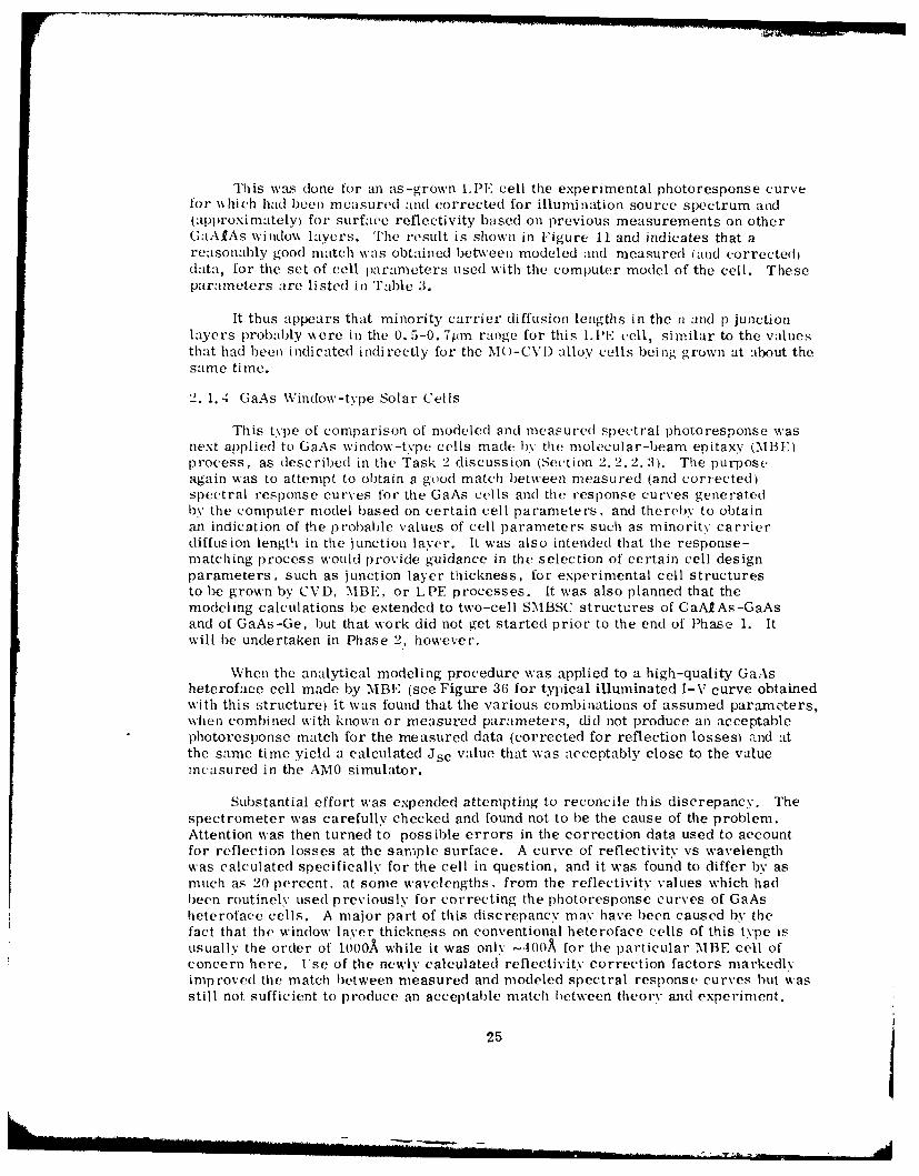
This was (lone for an as-grown L.PF cell the experimental photoresponse curvefor which had been measured and corrected for illumination source spectrum and(approximately) for surface reflectivity based on previous measurements on otherGaAfAs window layers. The result is shown in Figure 11 and indicates that areasonably good match was obtained betwveen modeled and measured (and correctebdata, for the set of cell parameters used with the computer model of the cell. Theseparameters are listed in Table 3.
It thus appears that minority carrier diffusion lengths in the n and p junctionlayers probably were in the 0.5-0. 7pm range for this lt 1.: cell, similar to the valuesthat had been indicated indirectly for the M()-CV I) alloy cells being grown at about thesame time.
2. 1. 4 GaAs Window-type Solar Cells
This type of comparison of modeled and measured spectral photoresponse wasnext applied to GaAs window-t vpe cells made by the molecular-beam epitaxy (MBE)process, as described in the Task 2 discussion (Section 2. 2.2. 3). The purposeagain was to attempt to obtain a good match between measured (and corrected)spectral response curves for the GaAs cells and the response curves generatedby the computer model based on certain cell parameters, and thereby to obtainan indication of the probable values of cell parameters such as minority carrierdiffusion length in the junetion layer. It was also intended that the response-matching process would provide guidance in the selection of certain cell designparameters, such as junction layer thickness, for experimental cell structuresto be grown by CVD, MBE, or LPE processes. It was also planned that themodeling calculations be extended to two-cell SMBSC structures of GaAfAs-GaAsand of GaAs-Ge, but that work did not get started prior to the end of Phase 1. Itwill be undertaken in Phase 2, however.
When the analytical modeling procedure was applied to a high-quality GaAsheteroface cell made by MIBE (see Figure 36 for typical illuminated I-V curve obtainedwith this structure) it was found that the various combinations of assumed parameters,when combined with known or measured parameters, did not produce an acceptablephotoresponse match for the measured data (corrected for reflection losses) and atthe same time yield a calculated asc value that was acceptably close to the valuemeasured in the AMO simulator.
Substantial effort was expended attempting to reconcile this discrepancy. Thespectrometer was carefully checked and found not to be the cause of the problem.Attention was then turned to possible errors in the correction data used to accountfor reflection losses at the sample surface. A curve of reflectivity vs wavelengthwas calculated specifically for the cell in question, and it was found to differ by asmuch as 20 percent. at some wavelengths, from the reflectivity values which hadbeen routinely used previously for correcting the photoresponse curves of GaAsheteroface cells. A major part of this discrepancy may have been caused by thefact that the window laver thickness on conventional heteroface cells of this type isusually the order of 1000A while it was only -1100A for the particular MBE cell ofconcern here. Use of the newly calculated reflectivity correction factors markedlyimproved the match between measured and modeled spectral response curves but wasstill not sufficient to produce an acceptable match between theory and experiment.
25
~ -
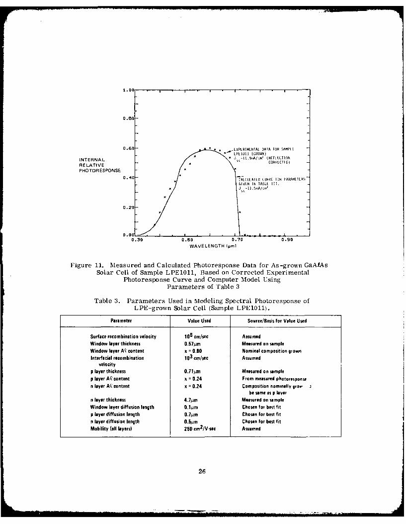
1.oc00I
0.60- K K LXPLRIMLNdIAL DATA FURl SAMI'LLK ~ LLIOII (GROWN)
INTERNAL x .~f' (RER~LCUIONRELATIVE x CQORRECI[D)
P HO TOR ESPON SE
0.40- CALCUIAILD CUI<VE IOR IAkAMITELR- GIVEN IN TABLE 111.
0.20-
0.30 0.50 0.70 0.90
WAVELENGTH (Am)
Figure 11. Measured and Calculated Photoresponse Data for As-grown GaAlAsSolar Cell of Sample LPE1O11, B~ased on Corrected Experimental
Photoresponse Curve and Computer Model UsingParameters of Table 3
Table 3. Parameters Used in Modeling Spectral Photoresponse ofLPE-grown Solar Cell (Sample LPE1O11).
Parameter Value Used Source/Basis for Value Used
Surface recombination velocity 106 cm/sac AssumedWindow layer thickness 0.57jum Measured on sampleWindow layer M content X = 0.80 Nominal composition grownInterfacial recombination i 3 cm/sec Assumed
velocityp layer thickness 0.7lpni Measured on sample
layer A( content x = 0.24 From measured photoresponse
n layer A content x = 0.24 Composition nominally grov' jbe same as p layer
n layer thickness 4.7prn Measured on sampleWindow layer diffusion length 0.lpmn Chosen for best fitp layer diffusion length 0.7pim Chosan for best fitn layer diffusion length 0.Sjam Chosen for best fitMobility (all layers) 250 cm2/V-sgc Assumed
26
Another attempt to improve the match was based on the argument that such athin window might be only partially effective in mitigating the short-wavelength lossesresulting from high surface recombination velocity. A sufficiently thin window couldallow an excessive number of electrons to tunnel through the barrier and recombineat the GaAf As/air interface. To model this possibility, a range of interfacerecombination velocities from 10 to 3 x 105 cm sec- was examined parametrically.Again it was not possible to obtain an acceptable match between measured andmodeled spectral response while simultaneously satisfying the constraint imposedby the measured Jsc.
The problem had not been fully resolved by the end of the Phase 1 reportingperiod. It appears that the most likely cause of the problem, however, is inadequatedata on the surface reflectivity of the specific cell involved. This would be remediedif specific reflectivity measurements were made for each cell examined.
27
. .- .
2.2 GaAs-Ge SMBSC TECHNOLOGY DEVELOPMENT
The GaAs-Ge materials system is naturally lattice-matched, so a Ge-GaAsheterostructure tunnel junction could provide the solution to the problem of providinglow-resistance current conduction across the interface of stacked GaAs and Ge cells.It would also be possible for this conducting tunnel junction to be entirely withinthe upper cell (GaAs) material.
This system also provides the opportunity for depositing the two cells on arelatively lower-cost material (viz, Ge) as well as one that is more robust and thusbetter able to resist process handling. One objective of this task was to deter-mine which of the two possible substrate materials - Ge or GaAs - is more suitablefor use in the two-cell SMBSC.
The program plan called for deposition of n+GaAs on p+Ge substrates andp+Ge on n+GaAs substrates to be undertaken first, to establish the growth conditionsrequired for the conducting (nonrectifying) junctions in both cases. Emphasis was tobe placed on determining deposition temperatures and subsequent heating cycles thatwould produce high interface doping concentrations and abrupt composition transitions.The dominant conduction mechanism was expected to be band-to-band tunneling, whichwould be investigated sufficiently to establish the conditions for obtaining the requiredlow-resistance contact.
The growth of GaAs solar cell structures on Ge substrates was then to beundertaken, to establish the conditions for obtaining high-quality GaAs cell perform-ance. Procedures and deposition conditions compatible with the requirements of thenonrectifying interfaces were to be emphasized and an optimum procedure sought.
Next, Ge solar cells were to be grown on Ge substrates, and conditions forobtaining high-efficiency Ge cell performance identified. Particular emphasis was tobe placed on achieving high efficiency with surface doping concentrationscompatible with the established requirements of the nonrectifying interfaces.
Following successful achievement of those specific tasks, the entire set ofdeposition procedures was to be integrated for the growth of the two-cell (GaAs and Ge)SMBSC structure on Ge substrates. The required cell fabrication procedures were tobe developed, and the resulting two-cell assembly then characterized (Task 6) and itsproperties carefully assessed.
It was intended that Ge p-n junction cells would also be grown in an invertedconfiguration on GaAs substrates, with the resulting structure nGe/p+Ge/n 4 GaAs.Photovoltaic characterization of such a structure would be accomplished by obtainingfront access to the p'Ge layer by selective etching or by contacting it through then+GaAs. Layer thicknesses and doping concentrations were to be chosen for bestphotovoltaic device performance, after which comparison with the performance ofGe junction cells on Ge substrates would be made.
Following successful fabrication of these Ge cells on GaAs (assuming therequired growth conditions for the nonrectifying interfaces were by that timeestablished, as discussed above), the two-cell (GaAs and Ge) SMTBSC assembly would
28
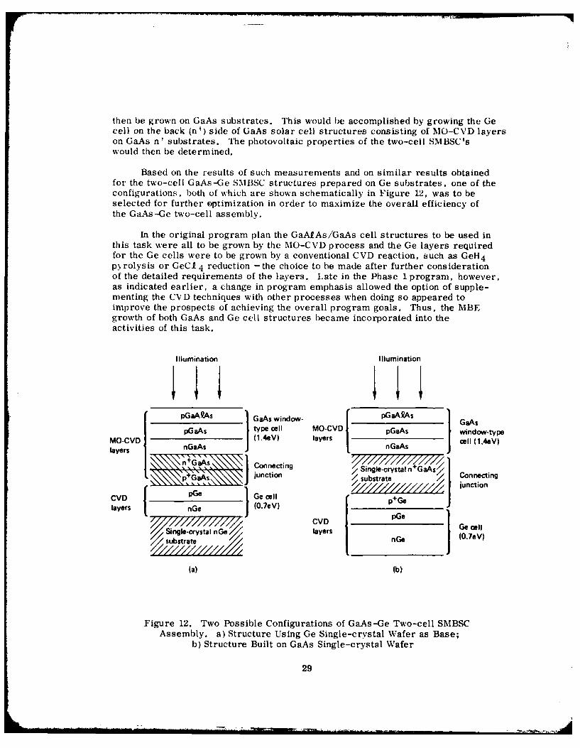
then be grown on GaAs substrates. This would be accomplished by growing the Ge
cell on the back (n+) side of GaAs solar cell structures consisting of MIO-CVD layers
on GaAs n' substrates. The photovoltaic properties of the two-cell SMBSC's
would then be determined.
Based on the results of such measurements and on similar results obtained
for the two-cell GaAs-Ge SMBSC structures prepared on Ge substrates, one of the
configurations, both of which are shown schematically in Figure 12, was to be
selected for further optimization in order to maximize the overall efficiency of
the GaAs-Ge two-cell assembly.
In the original program plan the GaAfAs/GaAs cell structures to be used in
this task were all to be grown by the MO-CVD process and the Ge layers required
for the Ge cells were to be grown by a conventional CVD reaction, such as GeH 4
p rolysis or GeC1 4 reduction - the choice to he made after further considerationof the detailed requirements of the layers. Late in the Phase 1 program, however,
as indicated earlier, a change in program emphasis allowed the option of supple-
menting the CVD techniques with other processes when doing so appeared to
improve the prospects of achieving the overall program goals. Thus, the MBE
growth of both GaAs and Ge cell structures became incorporated into the
activities of this task.
Illumination Illumination
pGaAQ As GaAs window- pGaA9As GaAs
pGaAs type cell MO-CVD pGaAs window-typeMO-CVD I (1.4eV) layers I cell (1.4eV)
layers nGaAs nGaAs
n~Ga~sjun ctin g Single-crystal n +Ga / 1junction / substrate / Connecting" " S\,\\\\\ junction
CVD fpGe 1Ge cel junctolayers nGe (0.7eV) f pGe
'},/_/ys//////G7 CVDpeSingle-crystal nGe layers Ge mellsubstrate nGe
(a) (b)
Figure 12. Two Possible Configurations of GaAs-Ge Two-cell SMBSC
Assembly. a) Structure Using Ge Single-crystal Wafer as Base;b) Structure Built on GaAs Single-crystal Wafer
29
This section contains descriptions of the preparation and characterizationof GaAs solar cells made by MO-CVD and by MBE techniques; the preparationand characterization of Ge solar cells made by CVD, MBE, and thermal diffusiontechniques; the preparation and evaluation of connecting intercell junctionstructures made by MO-CVD and MBE methods; and the fabrication of experimentalGaAs-Ge SMBSC structures.
2. 2. 1 Properties of GaAs-Ge Interface
Of the two possible configurations to be investigated for this two-cell SMBSC -one on a GaAs substrate and one on a Ge substrate - the most desirable one is thatinvolving the Ge substrate. In that configuration a GaAs cell is grown on a Ge cellon the Ge substrate, thus utilizing the larger-area less brittle Ge wafers and allowinghigher overall yields in the device fabrication process.
A major requirement for successful use of this configuration is growth of anabrupt and structurally perfect interface between the GaAs and the Ge, especially ifthe connecting junction between the two cells is to be a tunneling heterojunction.A series of samples consisting of thin (-400A) layers of GaAs on (100)-orientedsingle-crystal Ge substrates was grown by MO-CVD. The composition of thesefilms near the interface was analyzed by Auger electron spectroscopy combinedwith simultaneous etching of the sample surface by argon ion sputtering. Theapparent widths of the GaAs-Ge heterostructure transition regions, as determinedby the spatial distribution of the principal chemical species involved (viz, Ga, As,and Ge, as well as oxygen), were found to be dependent upon the particular growthconditions employed during the initiation of the GaAs layer growth on the Ge sub-strate surface. The minimum "interface width" of -45A was determined to occurfor films prepared with the TMGa and the arsine (ASH 3 ) introduced simultaneouslyinto the deposition chamber to start the GaAs layer growth.
Those growth conditions were then used to deposit GaAs p-n junction structuresand complete GaAlAs-GaAs heteroface solar cell structures on n-type (0.001-0.040 ohm-cm) Ge single-crystal substrates, described in Section 2.2.2 below.
Although some experimental n+ GaAs/p+Ge heterostructures were grown earlyin the program for preliminary evaluation, attention shifted at an early date ton+/p+ as well as p+/n+ structures grown entirely in GaAs layers on both GaAs and Gesingle-crystal substrates, for possible use as the conducting tunnel junction betweencells in the GaAs-Ge SMBSC. Such n+GaAs/p-GaAs structures were also used insome of the first GaAlAs-GaAs two-cell SMBSC's, as described in Sections 2.4.2and 2. 4. 3. The preparation and properties of these GaAs n+/p+ and p+n 4 structuresare discussed in Section 2. 2. 4.
2.2.2 GaAs Solar Cells for GaAs-Ge SMBSC's
The MO-CVD parameters found to produce the most abrupt transition from theGe substrate to the deposited GaAs film in the heterostructure samples described inSection 2.2. 1 were used to prepare GaAs p-n junction structures on n-type Ge (100)-oriented substrates as well as complete GaAs heteroface solar cell structures (with
30
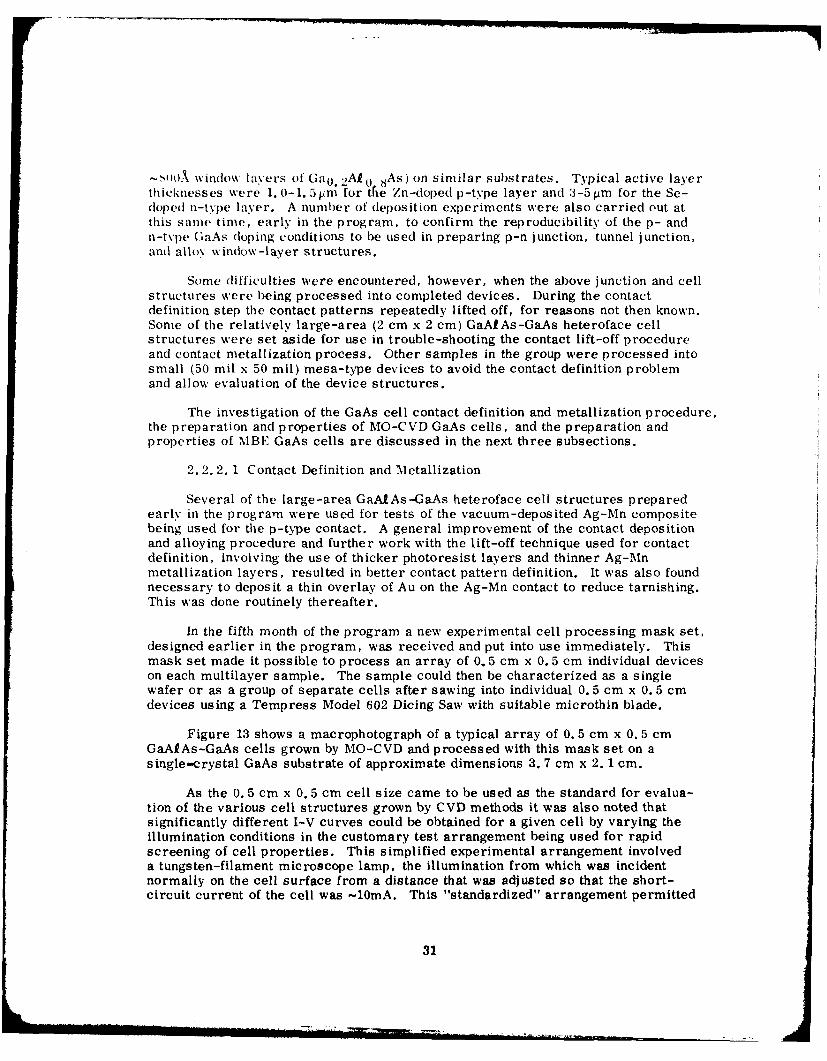
~-,(,A ) window layers of Ga 0 . 2A I () As) on similar substrates. Typical active layerthicknesses were 1. 0-1. 5pnm for tie Zn-doped p-type layer and 3-5Wm for the Se-doped n-tYpe layer. A number of deposition experiments were also carried out atthis same time, early in the program, to confirm the reproducibility of the p- andn-tv'pe (aAs doping conditions to be used in preparing p-n junction, tunnel junction,and alloy window-layer structures.
Some difficulties were encountered, however, when the above junction and cellstructures were being processed into completed devices. During the contactdefinition step the contact patterns repeatedly lifted off, for reasons not then known.Some of the relatively large-area (2 cm x 2 cm) GaAf As-GaAs heteroface cellstructures were set aside for use in trouble-shooting the contact lift-off procedureand contact metallization process. Other samples in the group were processed intosmall (50 mil x 50 mil) mesa-type devices to avoid the contact definition problemand allow evaluation of the device structures.
The investigation of the GaAs cell contact definition and metallization procedure,the preparation and properties of MO-CVD GaAs cells, and the preparation andproperties of MBE GaAs cells are discussed in the next three subsections.
2.2.2.1 Contact Definition and Metallization
Several of the large-area GaAI As-GaAs heteroface cell structures preparedearly in the program were used for tests of the vacuum-deposited Ag-Mn compositebeing used for the p-type contact. A general improvement of the contact depositionand alloying procedure and further work with the lift-off technique used for contactdefinition, involving the use of thicker photoresist layers and thinner Ag-Mnmetallization layers, resulted in better contact pattern definition. It was also foundnecessary to deposit a thin overlay of Au on the Ag-Mn contact to reduce tarnishing.This was done routinely thereafter.
In the fifth month of the program a new experimental cell processing mask set,designed earlier in the program, was received and put into use immediately. Thismask set made it possible to process an array of 0. 5 cm x 0.5 cm individual deviceson each multilayer sample. The sample could then be characterized as a singlewafer or as a group of separate cells after sawing into individual 0. 5 cm x 0. 5 cmdevices using a Tempress Model 602 Dicing Saw with suitable microthin blade.
Figure 13 shows a macrophotograph of a typical array of 0. 5 cm x 0. 5 cmGaAf As-GaAs cells grown by MO-CVD and processed with this mask set on asingle-crystal GaAs substrate of approximate dimensions 3. 7 cm x 2. 1 cm.
As the 0. 5 cm x 0.5 cm cell size came to be used as the standard for evalua-tion of the various cell structures grown by CVD methods it was also noted thatsignificantly different I-V curves could be obtained for a given cell by varying theillumination conditions in the customary test arrangement being used for rapidscreening of cell properties. This simplified experimental arrangement involveda tungsten-filament microscope lamp, the illumination from which was incidentnormally on the cell surface from a distance that was adjusted so that the short-circuit current of the cell was -10mA. This "standardized" arrangement permitted
31
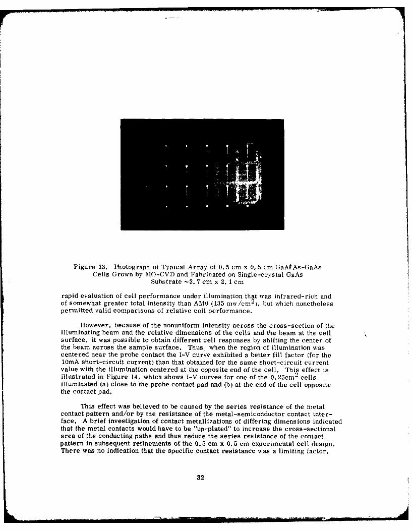
Figure 13. Photograph of Typical Array of 0. 5 cm x 0. 5 cm GaAI As-GaAsCells Grown by M\,O-CVD and Fabricated on Single-crystal GaAs
Substrate '-3. 7 cm x 2. 1 cm
rapid evaluation of cell performance under illumination that was infrared-rich andof somewhat greater total intensity than AMIO (135 mw/cm 2 , but which nonethelesspermitted valid comparisons of relative cell performance.
However, because of the nonuniform intensity across the cross-section of theilluminating beam and the relative dimensions of the cells and the beam at the cellsurface, it was possible to obtain different cell responses by shifting the center ofthe beam across the sample surface. Thus, when the region of illumination wascentered near the probe contact the 1-V curve exhibited a better fill factor (for thel0mA short-circuit current) than that obtained for the same short-circuit currentvalue with the illumination centered at the opposite end of the cell. This effect isillustrated in Figure 14, which shows I-V curves for one of the 0. 25cm 2 cellsilluminated (a) close to the probe contact pad and (b) at the end of the cell oppositethe contact pad.
This effect was believed to be caused by the series resistance of the metalcontact pattern and/or by the resistance of the metal-semiconductor contact inter-face. A brief investigation of contact metallizations of differing dimensions indicatedthat the metal contacts would have to be "up-plated" to increase the cross-sectionalarea of the conducting paths and thus reduce the series resistance of the contactpattern in subsequent refinements of the 0. 5 cm x 0. 5 cm experimental cell design.There was no indication that the specific contact resistance was a limiting factor.
32
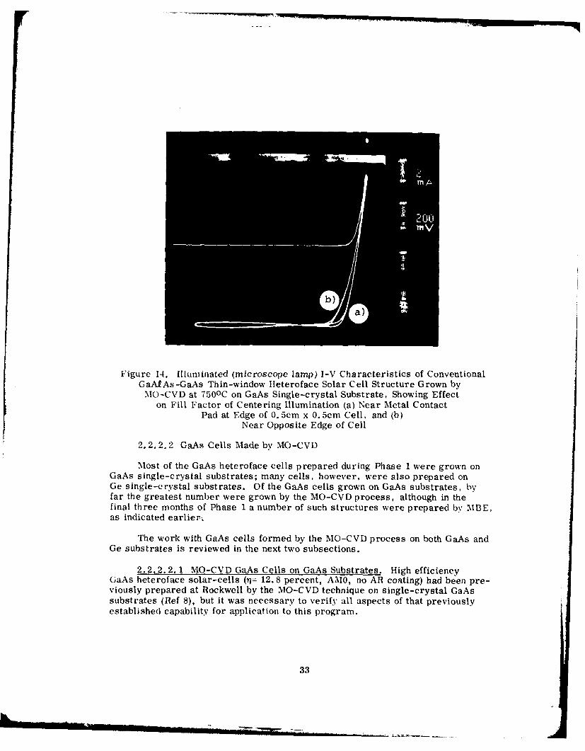
Figure 14. Illuminated (microscope lamp) I-V Characteristics of ConventionalGaAIAs-GaAs Thin-window Heteroface Solar Cell Structure Grown by
MG-CVD at 750 0 C on GaAs Single-crystal Substrate, Showing Effecton Fill Factor of Centering Illumination (a) Near Metal Contact
Pad at Edge of 0.5cm x 0.5cm Cell, and (b)Near Opposite Edge of Cell
2.2.2.2 GaAs Cells Made by MO-CVD
Most of the GaAs heteroface cells prepared during Phase 1 were grown onGaAs single-crystal substrates; many cells, however, were also prepared onGe single-crystal substrates. Of the GaAs cells grown on GaAs substrates, byfar the greatest number were grown by the MO-CVD process, although in thefinal three months of Phase 1 a number of such structures were prepared by MBE,as indicated earlier;
The work with GaAs cells formed by the MO-CVD process on both GaAs andGe substrates is reviewed in the next two subsections.
2.2.2. 2. 1 MO-CVD GaAs Cells on GaAs Substrates. High efficiencyGaAs heteroface solar-cells (q= 12. 8 percent, AMO, no AR coating) had been pre-viously prepared at Rockwell by the MO-CVD technique on single-crystal GaAssubstrates (Ref 8), but it was necessary to verify all aspects of that previouslyestablished capability for application to this program.
33
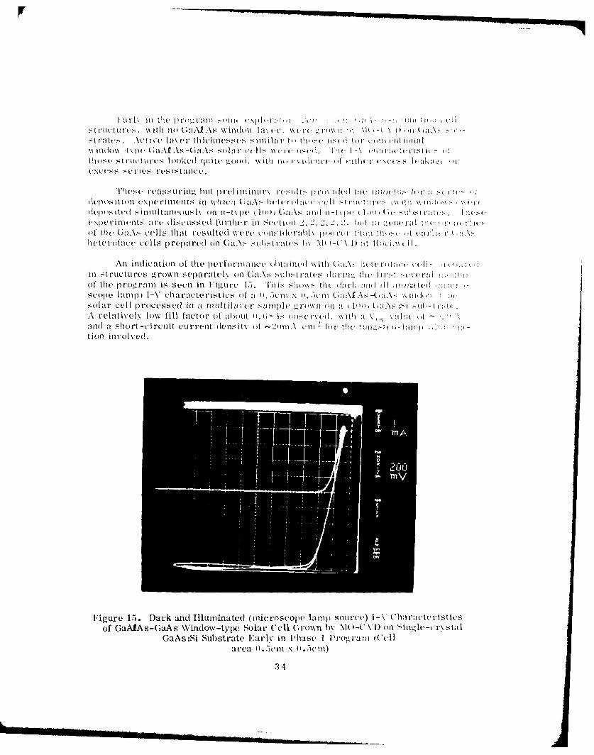
St Iticki tI .c 1wh no t IaAQ \s wt'io\ Im cr,~ \,t ( 1t I (\I .I \I Ik Mt 1) ii 1St (-:t(s S lcive knla t iitcllnssct s Stilhit III tht)5 [Ort it (l II i2tInil
\\ ioldiu -t\j Gi.(aA2A - A soi I. ccll \I, (.I- i ti ii l P'n I -\ et t(,I iti~
t 110SI StII'L ttL' t IV' liI ok quitc -oo I tthII u. ( t it ( i t tI IItI It s I- (.;I k iKL(
le ()si ese (-)vrsonlits I nt1,0 it)IIt.tt\ ttS1V111 ts' It itCCII Ithe in em It 1 H it . \
dIephiS ited S ill I ttnVoWS1\Ol1 -t \ Ie ( II ), G;~ Iu ]t n-I t ( In ( HI -,L Isl:teS ItsVNIPCI11inieutts it-( (liSCktSsetI tktrtlet ill Secktionl 2.2",2".2.. it hut :] Lcitfl 01 ; tI t<.i'' Its01 thyta~ G.4Cells thait I-CSLttCe \\(' otii c lttl)l pit.(1 rt thuist -I c I :Vhete rotace cel Is 1)re.parcd Onl GIaA S o~hS t r'ZitC. I )\ M( :~V)it H I .~cI
Ali indlicat ion of the lperfortuatkt Olit:0iiel 'Itith G(niA-\eeiw II'( t IIill Szt t'tCtures I2, rown scparatey Onl GaAs',l t s I-rt(S (LItt the tt>-t 1t 1-:1 ! !1!
ofthe p~rogram is SeeIf-l inl liIII.te 1.). TliS Shm s the, diarl, :ift 11Il 41v in ma tI
scope lamp) I-\ cha rncte ristit's (if a, O.5cm x O.c :i n iif1-as (solar cell processed inl a multilimIr -sawlv Olw in a1 1m),as ~ ih~ :
A relatively lo\\' fill factor Of a' n(Ut (I.G iS A ISCI [Ve. \V th : ~vleA-.and( a short-cirettlit CUrrent ilensitv oft -20MnA Ceni- lor the Iu2u-~t~ .tion inv'oIveil.
Figure 15. lDark and Illuminated (microscope lamp source) I- V Char11acteristicsof GaAftAs-Ga.As Window-type Solar Cell G;rown by M(iCV)on 'Singole-crvstal
GaAs:Si Substrate Earlv in Phase I P ro~ra in Weillarea (I.5cm x () * i m)
314
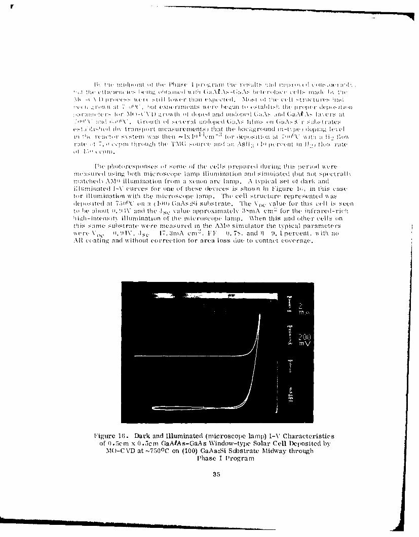
li 1it. w idpt'iit (11 t 11I h i t5 I pr-"t 1-11 ii lt 1 LIt511Iilp It 1i 0- II te t I c iilt 14. ic iiiI ,h Ic lit' I ;I I 111 (:iA A1- 1:i-i %' 'lc k-ll I: -I( i .' 0 '1,,
II!O - i t t. I lt-lk e .s> \ l-!l s t i e %%I\- th a -. p1ct- *M', -it 'I, -( -I >tlItd(il t5 i
'' 1l - 1-t '%% f :I1 t )i'4 t 4Xp II lit ~S N% -14 I I'I, Li I t - t I Ii Ii thIe Of -I' (It~ r -p( I Ii ('I)
t-lIl>-e I([ ,t ,I'(\ Drmht) I(asil niasreet Itidat tit hopckgrun li I G, pet I z)i% c I-vtII
In e it U re I Ius ill" Mithl i C ros cope I am n il i n i naZlt ion(11 (nd Si Il u LI1t1 ed (I ILt 11ttt Sp~Ct. ra11l.Ill :itcietlI A N itI11i liationl from11 a Xt-ntn IarCIa lmp1). A t,\ pical se t ol da.1rk andil IUIit11 i nate(I I -V c urves to r oeC0 t titSe (IC Vice', isS 110%% 1 in ligo0 re 1* in th is c-asevI(,I ' I tii i tion \v itli the -m ic ros cope lamip. The cell structUre rep resented %v asl4.-Jos ited at 751 oU oin a (lom 1 Ga:\s :S,-i stibst rate. Th~e V,, val ue for this cell is 5 C-ento i )v a1)otit t . 9l IV and the J-3 \ -,alue app1 rOxiImatV I 3 mnA cmi for the( inf rared- rich
12 hz -ntes tvill i iia~t ion of the microscope lamip. When this andi other cells onlthiSsam s,11 uLhst rate were inuasu red in the AMOI( simulator the typical parameters
e tre. V', 1)i. 9 V, -1 ,C 17. 3miA cm", 1:1. 0. 7s , and 71 9. 1 pe rcent. with noAR c oating" and withoult co)rrection for area loss due.10 to contact coverape.
Figure 16. Dark and Illuminated (microscope lamnp) I-V Characteristicsof 0.5cmn x 0.5cm GaAlAs-GaAs Window-type Solar Cell Deposited by
MIO-C VD at '-7500 C on (100) GaAs:Si Substrate Midway throughP~hase 1 Program
35
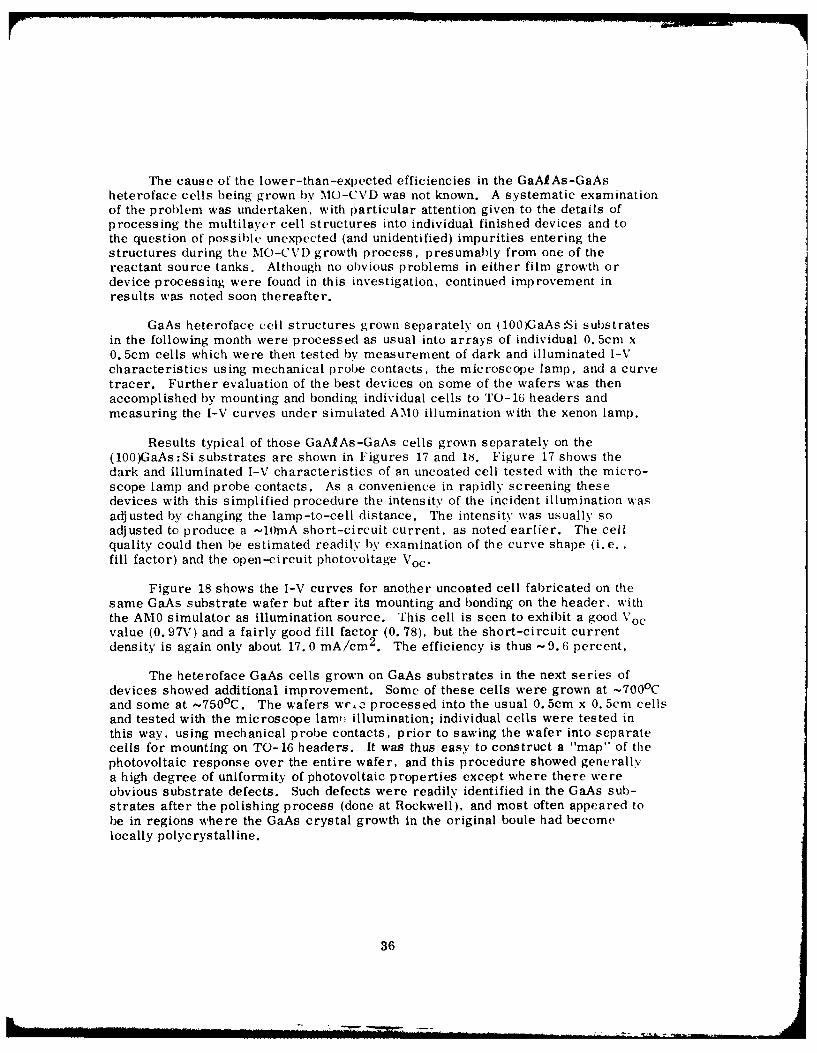
The cause of the lower-than-expected efficiencies in the GaA.As-GaAsheteroface cells being grown by MO-CVD was not known. A systematic examinationof the problem was undertaken, with particular attention given to the details ofprocessing the multilayer cell structures into individual finished devices and tothe question of possible unexpected (and unidentified) impurities entering thestructures during the MO-CVD growth process, presumably from one of thereactant source tanks. Although no obvious problems in either film growth ordevice processing were found in this investigation, continued improvement inresults was noted soon thereafter.
GaAs heteroface cell structures grown separately on (100)GaAs:Si substratesin the following month were processed as usual into arrays of individual 0. 5cm x0.5cm cells which were then tested by measurement of dark and illuminated I-Vcharacteristics using mechanical probe contacts, the microscope lamp, and a curvetracer. Further evaluation of the best devices on some of the wafers was thenaccomplished by mounting and bonding individual cells to TO-16 headers andmeasuring the I-V curves under simulated AMO illumination with the xenon lamp.
Results typical of those GaAIAs-GaAs cells grown separately on the(100)GaAs:Si substrates are shown in Figures 17 and 18. Figure 17 shows thedark and illuminated I-V characteristics of an uncoated cell tested with the micro-scope lamp and probe contacts. As a convenience in rapidly screening thesedevices with this simplified procedure the intensity of the incident illumination wasadjusted by changing the lamp-to-cell distance. The intensity was usually soadjusted to produce a -10mA short-circuit current, as noted earlier. The cellquality could then be estimated readily by examination of the curve shape (i.e.,fill factor) and the open-circuit photovoltage Voc.
Figure 18 shows the I-V curves for another uncoated cell fabricated on thesame GaAs substrate wafer but after its mounting and bonding on the header, withthe AMO simulator as illumination source. This cell is seen to exhibit a good Vocvalue (0. 97V) and a fairly good fill factor (0. 78), but the short-circuit currentdensity is again only about 17.0 mA/cm 2 . The efficiency is thus - 9.6 percent.
The heteroface GaAs cells grown on GaAs substrates in the next series ofdevices showed additional improvement. Some of these cells were grown at -700 0 Cand some at -750 0C. The wafers wr., processed into the usual 0.5cm x 0.5cm cellsand tested with the microscope lamt, illumination; individual cells were tested inthis way, using mechanical probe contacts, prior to sawing the wafer into separatecells for mounting on TO-16 headers. It was thus easy to construct a "map" of thephotovoltaic response over the entire wafer, and this procedure showed generallya high degree of uniformity of photovoltaic properties except where there wereobvious substrate defects. Such defects were readily identified in the GaAs sub-strates after the polishing process (done at Rockwell), and most often appeared tobe in regions where the GaAs crystal growth in the original boule had becomelocally polycrystalline.
36
IL
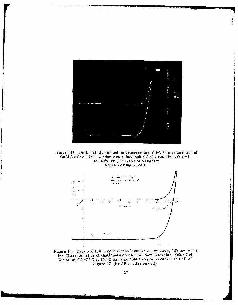
Figure 17. Dark and Illuminated (microscope lamp) I-V Characteristics ofGaAlAs-GaAs Thin-window Heteroface Solar Cell Grown by MO-CVD
at 750 0 C on (100)GaAs:Si Substrate(No AR coating on cell)
In
pCt P- -
I 2 4 I !
0] 0.2 .] 4 0 0.,6 0.7 0. 0 .00 volt aq :o
Figure 18. Dark and Illuminated (xenon laml) AMO simulator, 1:35 mw/cm 2 )
I-V Characteristics of GaAfAs-GaAs Thin-window tieteroface Solar CeUGrown by MO-CVD at 7500C on Same (100)(;aAs:Si Substrate as Cell of
Figure 17 (No AR coating on cell)
37
T' pical I-V characteristics (dark and illuminated by the microscope lamp) forthe better cells in samples grown at -700 0 C and -750 0 C are shown in Figures 19 and20, respectively. Comparison of these results with those of Figures 16 and 17 showsthat the later cells were generally improved over those previously prepared. Thelater cells all involved Te-doped n-type GaAs substrates, while most of the earliercells described were on Si-doped GaAs substrates. It did not necessarily appear,however, that the improvement in cell performance was related to the change to Te-doped substrates, especially since the latter have been found typically to have a highincidence of structural imperfections.
Also grown at about the same time were several conventional GaAlAs-GaAsheteroface solar cell structures having somewhat thinner p-type GaAs:Zn layers andthinner Ga0 .A1 Q. 8 As:Zn window layers than those normally grown. The p-typeactive layeWrs in these cells were - 0. 75 m thick instead of the usual 1.0 pm, and thewindow layers were -500A instead of the -1OOOX most often used in these cells. Itwould be expected that improved short-circuit current and better AMO spectralresponse would result for these modified cells. The dark and illuminated I-V char-acteristics for one of the 0. 5cm x 0. 5em cells fabricated in one of these structuresare shown in Figure 21, for illumination with the microscope lamp. It appears thatsomewhat improved photovoltaic response was indeed achieved by the modificationsin cell design.
As part of the investigation of possible causes of the lower-than-expected AMOefficiencies being obtained in the GaAs heteroface cells prepared by IO-CVD, anumber of the 0. 5cm x 0. 5cm GaAs window-type cells were characterized with thecalibrated Spectrolab Model XT-10 simulator (AMO, xenon source) at the RockvellSatellite Systems Division at Seal Beach, CA. The simulator used earlier atRockwell ERC involved an unfiltered 1000-watt xenon lamp, and this source isknown to have a spectral output that is not a very good match to the AMO spectrum.This raised the obvious question of the effect upon measured cell performance ofdepartures of the simulated AMO spectrum from the proper AM() spectrum, althoughfor most non-critical measurements the unfiltered lamp provided an acceptablemeasure of "AMO response."
The group of cells measured in the Seal Beach simulator involved four differentsubstrate wafers and had not been previously evaluated with the ERC simulator. Thesimulator output was set for 129 mw/cm 2 by means of a calibrated Si reference cell.For this AMO simulated insolation the cells measured had efficiencies of up to11. 5 percent, with no All coating. If a multiplying factor of 0. 95/0. 66 - 1.44 isapplied to correct for the anticipated effect of a good AR coating it follows that theabove maximum corresponds to an efficiency of 16. 6 percent with coating. Althoughthis is still not as high as the previous best performance achieved with such a cellmade at Rockwell by MO-CVD, the result did provide an adequate baseline referencefor comparison of the various SMBSC's under development in this program. Figure 22shows the fourth-quadrant I-V curve for the 11. 5 percent cell under AMO illuminationof 129 mw/cm 2 , as obtained in the above measurements.
38
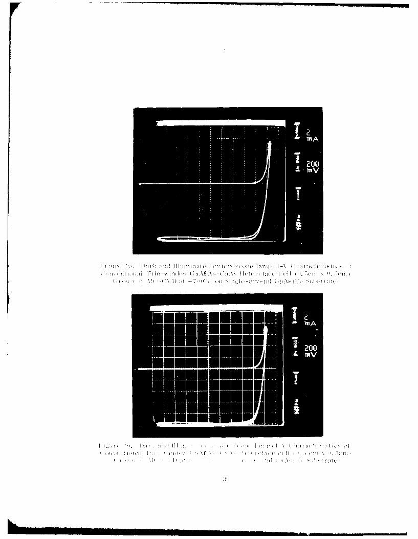
Ixrlk : I tll) i Ix (:i\ -(:I ic v lac n I K up: c .S!I
11 l t t h-E.d) ( I ...E.E E(-
I EEEEEEEEIIE..EEE.E
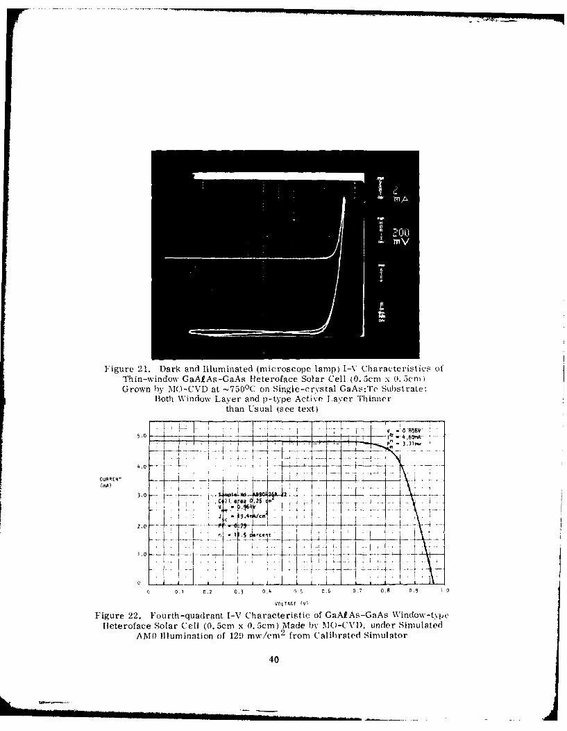
Figure 21. Dark and Illuminated (microscope lamp) I-V Characteristics ofThin-window GaAlAs-GaAs Heteroface Solar Cell (0. 5cm x 0. 5cm,Grown by MO-CVD at -750 0 C on Single-crystal GaAs:Te Substrate;
Both Window Layer and p-type Active Laver Thinnerthan Usual (see text)
vol.~ .BMW v
5.0 -d- -- ~ .. --- r .0P' 3.m 11
CURRENT 4.- L +7 iii ..
2.00
g. rce t
1.0_____ .L VL -i19
0J 0.2 0.3 0.4 0.5 0.6 0.7 . 0. 10
VOLTAGE (0~
Figure 22. Fourth-quadrant I-V Characteristic of GaAlAs-GaAs Window-t' \peHleteroface Solar Cell (0. 5cm x 0. 5cm) Made by TA1-CNVD, under Simulated
AMO Illumination of 129 mw/cm 2 from 'Calibrated Simulator
40
Shortly after the above cell structures were grown it was noted, by carefulSE.l and optical microscope examination, that the layer thicknesses in varioussingle-cell and two-cell SMBSC structures were much less than was expectedon the basis of the deposition parameters used. The apparent cause of this wasthat a new mass-flow controller had been installed in the TMG source line of thereactor system just prior to the growth of these structures, because of functionalproblems that had developed with the controller previously in use. The new unit,however, had evidently been miscalibrated at the factory (Tylan Corp., Torrance,CA) so that thicknesses of layers involving Ga as a constituent turned out to be quitcdifferent from expected values.
After this problem was corrected and the necessary growth parameters hadbeen reestablished, a number of conventional GaAlAs-GaAs thin-window heterofacesolar cell structures on GaAs substrates were prepared by deposition at 7500C.The structure (i.e., layer thicknesses and doping concentrations) of these com-posites was varied slightly to determine the effect of such parameter variationson the performance of the resulting cells. As customary, the wafers were pro-cessed into arrays of 0. 5cm x 0.5cm (0.25 cm 2 area) individual cells. Theresulting cells were evaluated using the microscope lamp and mechanical probes.
Typical I-V characteristics obtained for cells on some of the best wafersare shown in Figure 23. As in previous cell characterization using the microscopelamp the intensity was set to produce a short-circuit current of 10mA for the cellunder test. It can be seen that Voc values of 1. OV were obtained, with good curveshapes (fill factors).
Spectral response measurements were made on some of these GaAs cellsusing the grating spectrometer and detector system at ERC Anaheim. This equip-ment uses a 100-150 watt tungsten-halogen lamp in conjunction with a Spex I 4-metergrating spectrometer and appropriate focusing optics. The throughput of the systemoperating at 100.A resolution generates a short-circuit current density in a cell thatis approximately 10-3 x Jsc(AI0g). For accurate quantitative spectral responsedata the cells should be AR-coated, but accurate comparisons of individual cellson a given substrate wafer can be made without the coating. Data for photoresponseas a function of wavelength for both a reference cell and the experimental cell andquantum efficiency data for the reference cell are put into digital form and manipu-lated by a llewlett-Packard 9825A computer. The output is the response of theexperimental cell as a function of wavelength normalized for unit input intensity.
Figure 24 shows data for two conventional GaAfAs-GaAs thin-window hetero-face solar cells (0.5cm x 0.5cm) grown by MO-CVD at 7500C on a GaAs substrate(i. e., both cells are on a common substrate). One of the two cells is the cell theI-V curves for which are shown in Figure 23a. Coincidence of the point-by-pointspectral response data for the two cells is striking and attests to the uniformity ofresults obtained by the MO-CVD process over the area of a typical 2cm x .4 cmsubstrate. The sharp drop in response at long wavelengths corresponds to theexpected behavior at the bandgap energy of GaAs. Both cells maintain essentiallymaximum response for higher-energy illumination throughout the visible region,still exhibiting >80 percent of maximum response at wavelengths as shortas -0. 475 pm.
41
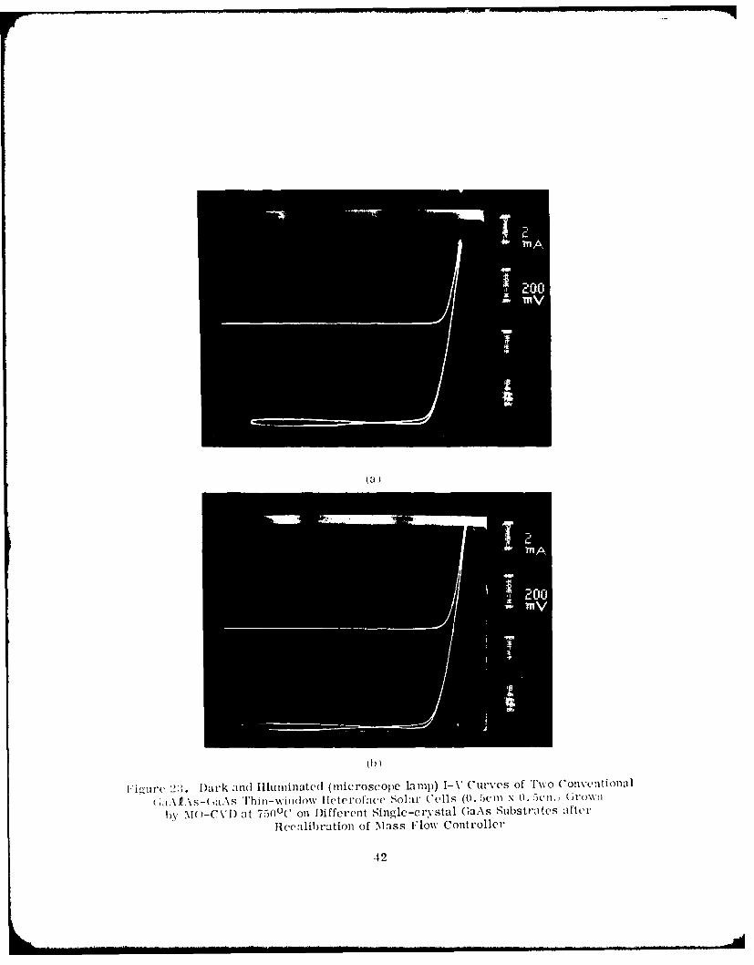
jFj(Ill( 2:, Dark and IllUminated (microscope 1,1111)) I- V (7Urve's Of TFWO ConVentionlal
I.\ P.'s- ( ;aA s 'Ph in-windo I lete. I'Iu Sola I:IIell s (0. 5cm x o. 5c n. Growii
by ]( )-CVI) at 7500(7 on D~ifferent Single-crystal GaAs Substrates -1ft Lr
Heccalibration of mass Fl'ow\ Controller
42
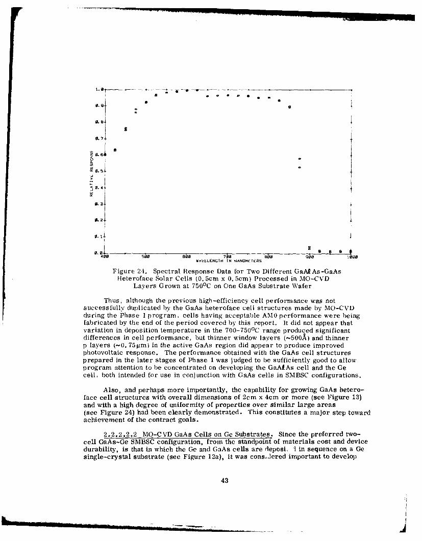
-. ------ ------ S
. . S
9 7
02. 4i0.4a a
III 2
0.11C
488 58 8&0 780 Boo 90 090WAVELENGTH IN NANOMETERS
Figure 24. Spectral Response Data for Two Different GaAMAs-GaAsHeteroface Solar Cells (0. 5cm x 0. 5cm) Processed in MO-CVD
Layers Grown at 750 0 C on One GaAs Substrate Wafer
Thus, although the previous high-efficiency cell performance was notsuccessfully duplicated by the GaAs heteroface cell structures made by MO-CVDduring the Phase 1 program, cells having acceptable AM0 performance were beingfabricated by the end of the period covered by this report. It did not appear thatvariation in deposition temperature in the 700-7500 C range produced significantdifferences in cell performance, but thinner window layers (-500.A) and thinnerp layers (-0. 75 fim) in the active GaAs region did appear to produce improvedphotovoltaic response. The performance obtained with the GaAs cell structuresprepared in the later stages of Phase 1 was judged to be sufficiently good to allowprogram attention to be concentrated on developing the GaAIAs cell and the Gecell, both intended for use in conjunction with GaAs cells in SMBSC configurations.
Also, and perhaps more importantly, the capability for growing GaAs hetero-face cell structures with overall dimensions of 2cm x 4cm or more (see Figure 13)and with a high degree of uniformity of properties over similar large areas(see Figure 24) had been clearly demonstrated. This constitutes a major step towardachievement of the contract goals.
2.2.2.2.2 MO-CVD GaAs Cells on Ge Substrates. Since the preferred two-cell GaAs-Ge SMBSC configuration, from the standpoint of materials cost and devicedurability, is that in which the Ge and GaAs cells are deposi, i in sequence on a Gesingle-crystal substrate (see Figure 12a), it was cons Jered important to develop
43
the capability for obtaining high quality GaAs cell structures on Ge by one or moreof the deposition techniques being used. Consequently, the first GaAs cell structuresprepared in this program were grown by the MO-CVD process on Ge substrates, aspointed out previously.
The GaAs MO-CVD growth parameters that had produced the most abrupttransition from Ge to GaAs at the growth interface in samples that had been analyzedby Auger electron spectroscopy (see Section 2. 2. 1) were used to prepare GaAs p-njunction device structures on low-resistivity (0, 001-0. 040 ohm-cm) n-type (100)-oriented Ge single-crystal wafers. Typical n layer thicknesses were 3-5rpm andp layer thicknesses were 1.0-1. 5p.m. Some of the structures also had Ga 0 .2A 0 . 8Aswindow layers g0. lpm thick. Problems were encountered in processing these firststructures into completed large-area cells, as noted earlier, due to contactadherence and lift-off difficulties.
To circumvent the large-area contact problem temporarily a number of small(50 mil x 50 mil) mesa-type devices were fabricated in these structures, some ofwhich were grown at -700oC and some at -750 0 C. Those grown at 750 0 C werefound to be considerably more leaky than those grown at the lower temperature,suggesting at first that MO-CVD growth of GaAs on Ge might best be done at lower-than-customary temperatures to avoid defect formation at the growth interface.Those devices grown at -700 0 C exhibited good forward and reverse I-V characteristics.
Some large-area (2cm x 2cm) cells grown on Ge substrates at -750oC weresuccessfully processed, including some with and some without GaAIAs windowlayers. Although the structures grown on GaAs substrates at about the same timeshowed relatively good I-V characteristics (neither excess leakage nor excessseries resistance), those grown on Ge substrates exhibited the same leaky I-Vcharacteristics as were seen for the small mesa devices mentioned above. Thefill factors were poor, so the efficiencies were very low.
Shortly thereafter, another group of GaAs p-n junction structures and GaAsheteroface solar cell structures was grown on (100)GaAs and (100)Ge n-type single-crystal substrates. The structures on Ge were deposited at 700 and 750 0 C, aswere those in the previous group. Small-area (50 mil x 50 mil) mesa devices with25 mil x 25 mil contact pads were again fabricated. As for the earlier group ofsimilar devices, those grown at 700 0 C had somewhat better (less leaky) I-V curvesthan did those grown at 7500 C.
One of the GaAs p-n junction structures was grown on a Ge substrate thathad been conted on the back surface (and also on the edges) with -1000A ofsputtered Si0 2 to attempt to prevent any interaction of the Ge substrate with theMO-CVD environment after initiation of GaAs deposition. This wafer was thenfabricated into small-area mesa diodes and their properties were compared withthose of similar devices grown on the uncoated Ge substrates. Improved resultswere achieved, so the procedure of coating Ge substrates to be used in the GaAsMO-CVD environment appeared to be a helpful one and thus was used for most Gesubstrates involved in GaAs depositions throughout the remainder of the program.
In the subsequent series of deposition experiments several GaAs thin-windowcell structures were grown simultaneously on n-type (Sb-doped) (100)-oriented Geand n-type (Si-doped) (100)-oriented GaAs substrates by the MO-CVD process.
44
-i
These structures were deposited at 700, 750, and 800 0 C. A few of the Ce substrateshad been previously coated with -1000A of sputtered SiO 2 . In addition, some GaAsp-n junction structures without GaAIAs window layers were grown on Ge:Sb sub-strates (some SiO2 -coated and some uncoated). The cell structures were processedinto 0.5cm x 0.5cm devices, while the simple junction structures were fabricatedinto small mesa diodes.
In general, the solar cells and junction diodes fabricated in GaAs grown onSiO 2 -coated Ge substrates in this group exhibited less leaky I-V characteristicsthan those on uncoated Ge substrates. However, all of the solar cells grown onGe substrates (coated or uncoated) had Voc values of only -0. 8V under illuminationby a laboratory microscope lamp, whereas cells grown on GaAs substrates typicallyexhibited Voc values of -0. 96V under the same illumination conditions. The causeof this difference was not established at the time.
Figure 25a shows the dark and illuminated (microscope lamp) I-Vcharacteristics of a GaAs p-n junction mesa diode (no GaAIAs window laver)grown on a Ge substrate that was uncoated. Figure 25b shows similar curves fora similar device grown on a Ge substrate having the SiO 2 coating (except on thedeposition surface). The 50 mil x 50 mil mesas had centrally located 25 mil x25 mil ohmic contacts on their top surfaces, as for earlier mesa devices.
Some of the samples in the above group were not processed into devices untilthe following month, at which time they were processed into the standard-size cellswith other, more recently grown, samples. Upon testing with the lkw xenon lamp(simulated AMO illumination) it was found that the cells on GaAs again had higherefficiencies than those grown simultaneously on Ge. Figure 26a shows the AMOphotoresponse of one of these cells grown on GaAs:Si and Figure 26b shows thedark and light I-V characteristics of a cell in the simultaneously grown multilayerstructure on SiO2 -coated Ge:Sb. These cell structures were grown at 700 0 C. NoAR coatings were used and no allowance was made in calculating the efficienciesfor the area shielded by the contact grid. The efficiency of the cell on the Gesubstrate is seen to be less than half of that of the cell on the GaAs substrate,primarily due to significantly lower Isc and Voc values although even the fill factoris better for the GaAs-based cell (0. 80) than for the Ge-based cell (0. 70).
Some attempts were then made to identify the possible cause(s) of thesepersistent differences. Semilogarithmic plots of current vs voltage were made forsome of the devices to compare the junction properties of the GaAs-based and theGe-based cells and to compare both with those of similar cells grown earlier inthe program. Figure 27a shows the forward (dark) I-V characteristic of aGaAlAs-GaAs solar cell structure grown on a GaAs:Si substrate and processedinto a completed device with this later group. Figure 27b shows the correspondingdata for a similar cell on a GaAs:Si substrate grown and processed several monthsearlier. (In both instances the data were obtained with the automatic plotter. ) Itis evident that the more recent cell shows considerably more leakage at lowvoltages. The current conduction appears ohmic at zero bias, suggesting asevere shunting problem. It was not established at the time whether this shuntingwas related to device fabrication or materials growth problems.
45
6Li
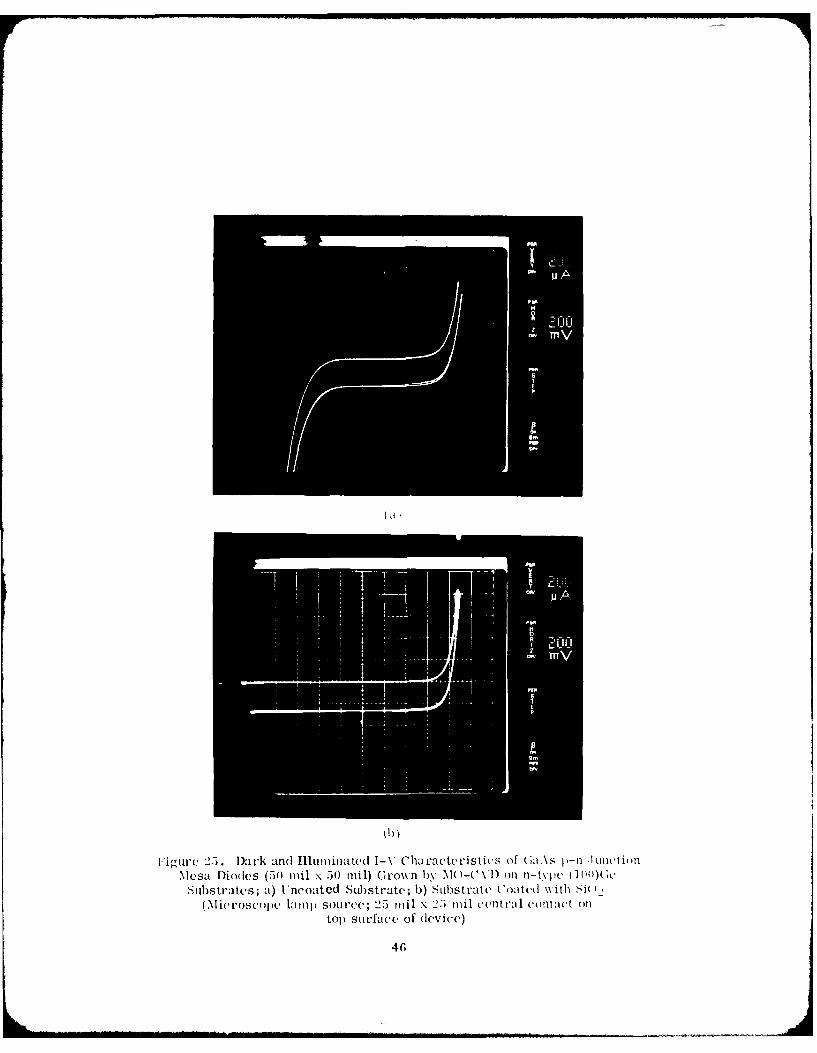
1.1r11Lr(, 23. Dar1k andl( 1Illa~tCel I- \ Cha racter1istics of G;a \s 11 Junction
Mesa D~iode~s (50 mil x 50 mil) Grown hy M( )-C VI on fl-typ' (*1 Oi)
Subhstrates; a) Uncoated SubIstrate,; 1)) SubIstrate (coatt'd with Si(MNicroiscope 1,111 mpsOLrc; 25 muli x 23 mil cen'rt ral ouct oil
top surface of (levie)
46
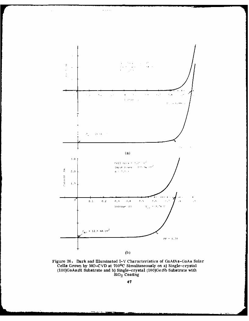
.4 - .,, .
(a)0.0 /
-' I A W
1'2ltAq , 6 " ' c .2
2.0
(b)
Figure 26. Dark and Illuminated I-V Characteristics of GaAIAs-GaAs SolarCells Grown by MO-CVD at 700 0C Simultaneously on a) Single-crystal(100)GaAs:Sl Substrate and b) Single-crystal (100)Ge:Sb Substrate with
S10 2 Coating
47
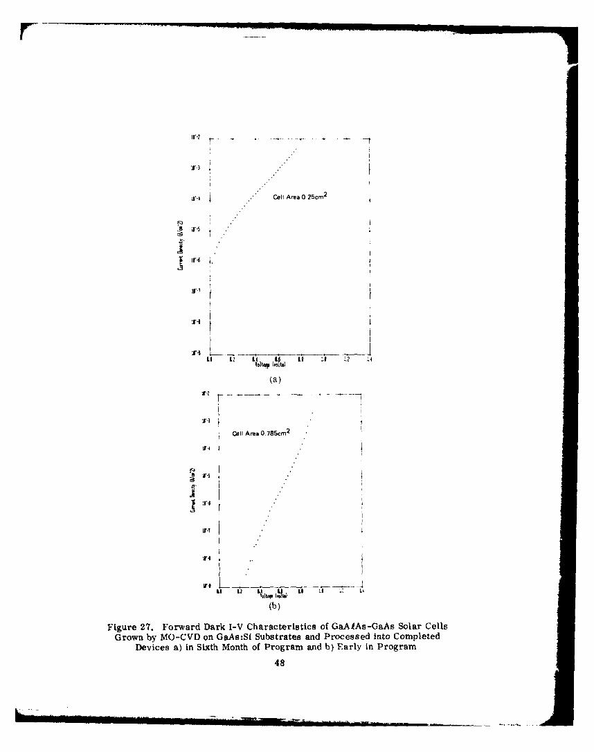
- . . -
Cell Area 0.25cm2
.11
jr-i
jj'-7
lf-i
(a)ir -2 F-
Cell Area 0.785cm2
j
ir-
1r- 2 A L Li
(b)
Figure 27. Forward Dark I-V Characteristics of GaAIAs-GaAs Solar CellsGrown by MO-CVD on GaAs:SI Substrates and Processed into Completed
Devices a) in Sixth Month of Program and b) Early in Program
48
While these investigations were in progress additional groups of GaAIAs-GaAsheteroface cell structures were prepared, with n-type (Sb-doped) (100)Ge and n-type(Si-doped) (100) GaAs substrates included for simultaneous deposition in each run.One group was deposited entirely at 700 0 C, and all of the Ge substrates were coatedwith -1000A of sputtered SiO on the back surface. A second group involved deposi-tion temperatures of 650 and 7OOC, again with the Ge substrates all previouslycoated with Si0 2 . Several separate runs were also made to grow similar cellstructures just on GaAs:Si substrates alone at 750 0 C, for comparison.
Some of the samples of the first of the above groups, grown at -700 0 C on bothGaAs and Ge (Si0 2 -coated) substrates, were processed separately into 0.5 cm x0. 5cm cells and were tested in individual chip form with probe contacts and themicroscope lamp. Representative dark and illuminated I-V curves for severalof these cells are shown in Figures 28 and 29.
Figure 28a shows the I-V curves of a GaAIAs-GaAs cell grown on (100)Ge:Sbat 6901C. The cells from this wafer were unique in that they were the first of thecells grown on Ge substrates in this program to show high values of Voc. Also,they showed relatively small leakage currents. The companion GaAIAs-GaAscells grown simultaneously on GaAs:Si substrates also exhibited good I-V curves,as shown in Figure 28b.
Figure 29a shows a similar GaAIAs-GaAs cell grown on a Ge:Sb substrateat .,700 0 C, but the initial (i. e. , predeposition) conditions used in the growth of theGaAs layer in this case were different from the conditions used for the growthof the cell structures represented in Figure 28. The Voc of the Ge-based cellin Figure 29a is much lower than that of the cell in Figure 28a.
The companion cell grown on GaAs:Si simultaneously with the one shown inFigure 29a, however, has a good Voc, as shown in Figure 29b, but its leakagecurrent is seen to be higher than that in the cell of Figure 28b.
The question of the effect of changes in the predeposition conditions in thereactor, as employed in preparation of these samples, was examined further.The normal procedure for GaAs growth on GaAs substrates by MO-CVD is tointroduce AsH 3 into the deposition chamber several minutes prior to the intro-duction of the TMG. Some of the GaAs films (Figure 28) were grown by thisstandard procedure and others (Figure 29) were deposited with the AsH 3 beingintroduced only a few seconds ahead of the TMG, thus avoiding the formation ofuncombined Ga metal inclusions at the interface yet reducing the time for Ge-Ash 3 reactions to occur.
A separate set of undoped GaAs fiLms was deposited at -700 0 C on (100)-oriented n-type Ge:Sb substrates that h:td previously been examined by x-raytransmission topography so that structural characteristics of the GaAs filmscould be correlated with structural properties of the Ge substrates. Some ofthe films were grown with the standard predeposition procedure and some withthe short AsH3 exposure, to attempt to identify any structural differences inthe films for the two types of substrate surface treatment. Additional window-type GaAs cell structures were grown on (100) GaAs and (100) Ge substratessimultaneously at -750 0 C for use in this investigation; several were prepared withthe standard procedure and others with the modified procedure.
49
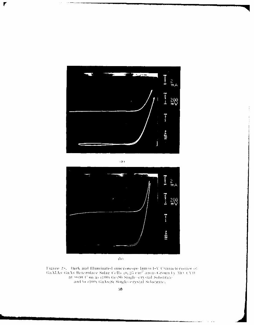
1 ,- I, I r v 2 ' 1 I),irk nnI(I III tifiiflite l (mit i ( flj) I 11 i I -V Chnr cc i is ('I(;\\~- I> I ceI('0CftaL Sol ar Mels O 5U2a dw WI
att -,,90 C onl 11) I(IM1 GeS iLttv~lsihst m:Itam] 111 1100)h~s Single-crystal Sis ie
50
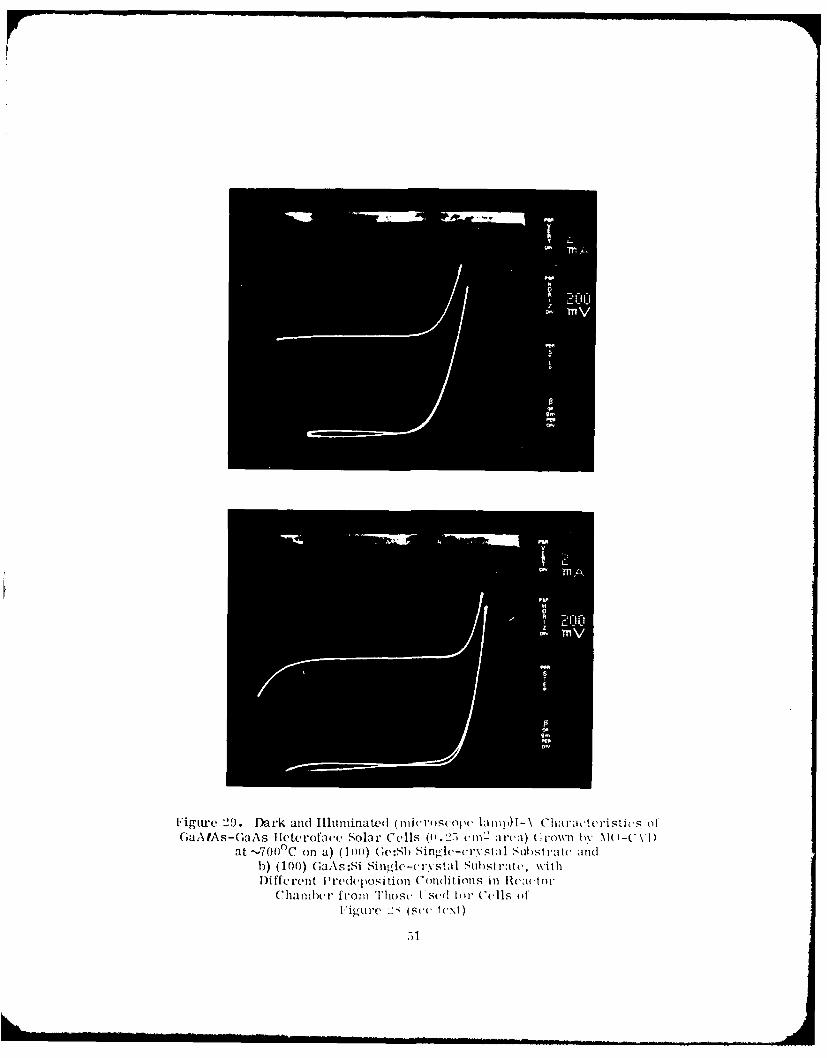
Figure 29. Dark and Illuminated ( micrPoscope Lam VC ha ract li stie s otGaAfAs-('aAs Tifteroface Solar Cells ((. 11e2 a rea) Grown 1) ,I v - VI)
at -700 0 C on a) (10(0) (;ec:Sh) Singe-u ' v stal Substrate aIndb) (100) GaAs :Si Sing-le- rysta I Stihst rat(', \kithD~ifferPent P'red'posi tion Conditions in R~eactIor
C1ha mix'wi from Those 1sed to Cells of
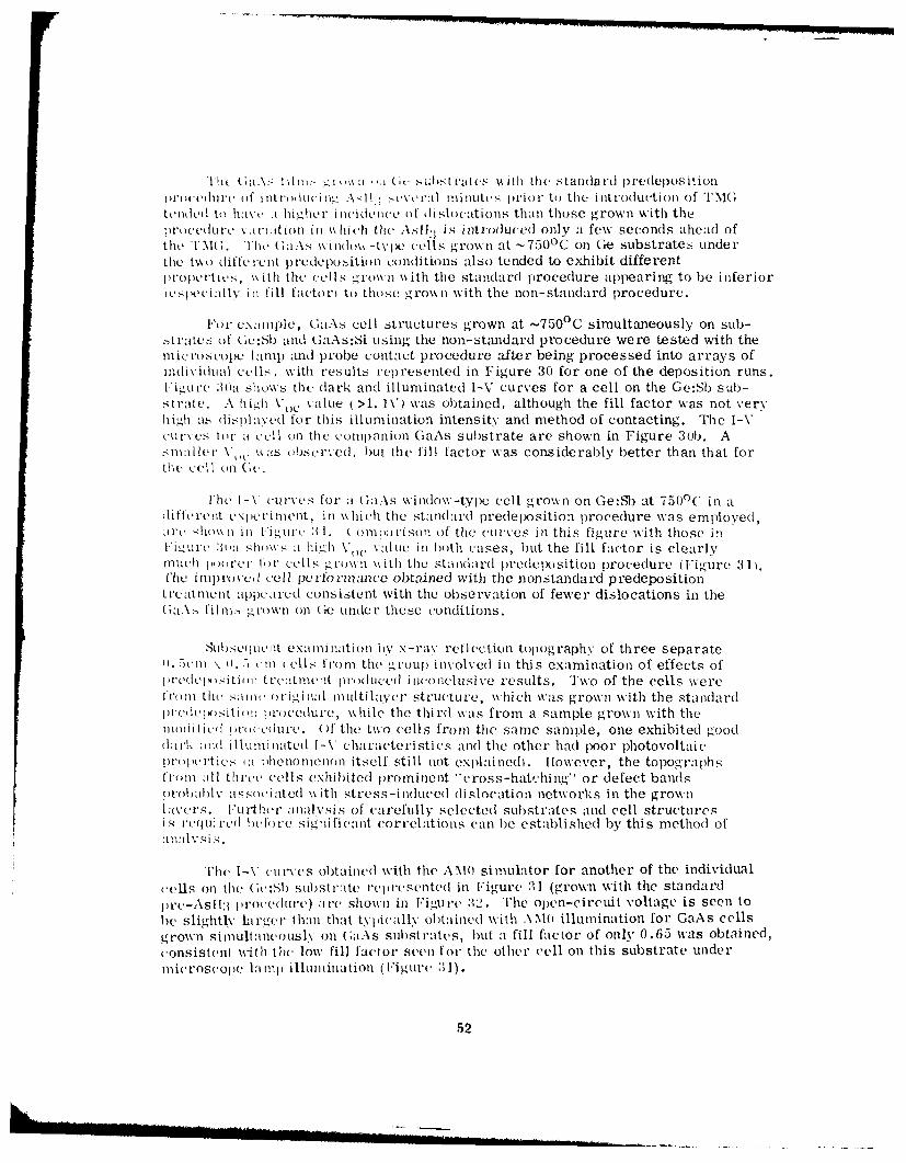
i I (~iA.-eI ti I-in i n ,n (It s Li , tvat es ]A itIh t h( -st4an dard predepos it ionlpriwedllre Of iot i'OklIli, A-< I; stI- ,11 'verallutts pror to the i ntrodu('tioll of TlM(;te lt' I to hA% k' a hi"1' r ((i tlidCflit' Of di SI(JLtatInS than those grown with thepri tedore wa% itiofu ili MX i ch the .XS113 is introtlu(Lil Only a few seconlds ahead ofthC '1MG. 'ihe' Ga3AS \M iod\\-t\,pe cells grown at -'75 0 tC on Ge substrates underthle two differenct 1 )redepObitioli conditions also tended to exhibit differentproperties', % i th the cell s t',o\\n with the standard procedure appearing to be inferiorI especiaik ill fill facto rl to thlose- growni with thle non-standard procedure.
For e\ai)iple, Ga_-s cell structures grown at -750 0 C simultaneously on sub-Sti'atCeS Of GC:Sb an1d Ga--S:Si uingl thle non-standard procedure were tested with theifliCioscope lam11p and probe contact procedure after being processed into arrays ofindividual cellsI with results represented in Figure 30 for one of the deposition runs.V:igo re 30a shows thle dlark and illuminated I-V curves for a cell on the Ge:S6 sub-strate. A highd VO vaIlue >1. 1\') w\as obtained, although the fill factor was not veryhighl as display.ed for this illumination intensity and method of contacting. The I-Vcllrves for aI ccli on the :omipanion GaAs substrate are shown in Figure 301). Asmll llcr %%aas Observed, but the fill factor was considerably better than that forthe Cell onl (;(,.
IHe 1-\ crvnes for a GaAs winldow-type cell growni on Ge:Sb at 750 0 C inl adlifferent ext en mlent, inl \\ h thle stanidard predeposition p~rocedure was employed,ire sh;Io\In inlli Vicr. 3 1. ( omipa ri soi Of the curves inl this fig-ure with those inl
Fig1 ore :) a: sh1O\\ S a1 hi'h \1 valioc inl hoth cases, but the fill factor is clearlymnuch pie re'()Ir cell" "'ro\\1 n i thl thle stzindard predepxsition procedure (Figure 31).Cibe imlprovudc cell perfoimuce obtained with the nonstandard predepositiontreatment appeared consistent wvith the observation of few~er dislocations in the(;1A.-,i fil i\n On GIC Undleri these conditions.
SLlh aqclt exam nilat ionl by x-rvrelcion topography of three separateI. cin \ 0. .cm c-llells- fromi thle group i ni-le l this examination of effects of
predclOsition t reatmetiit produced incon01clusive results. Two of the cells werefrin i thesain o rig] al i lti lae stutre, '~hi( -iws growin with the standardpredeI'j )siti ol procediure, while the tird wkas from a sample grown with theMini Cd iiWOC01lore. (if thle two cells fromn the same sample, one exhibited gooddar :111td i liiimi nated 1 -\' characteri sticts and thle other had poor photovoltaic-Ill' icrt io-s a phelln enon itself still not explaitnedl . fHowever, the topographsfromn all thiret cells exhibited prominent "cross-hatching'' or dlefect banudsprohlall ssociated w\ith stress-i ndluce dislocation nietworks in the grownI:avers. Fur1ther analyVsis Of c'arefuilly selected substrates and cell structuresis requiired before signiffic'anit correlations can he established by this method of
'The l-\' curve-s Obtained with the AMPI simiulator for another of the individual('(Us onl thle (Ic :SI subhstralte reclrcsentecl in F~igure 31 (grown with the standardpine-As 11:j prOC(du-C) are showni in lFigu inc 32. 'The open-circuit voltage is seen tohe slightly larger thanl that typically obtained wvith A Mo illumnination for GaAs cellsgro-wn si iiultan('iously on (taAS 5Std)St rates, butt a fill factor of only 0).65 w~as obtained,consist(flt with the low fill factor Seen for' thle other cll on this substrate underrini('ios('op ic inJI iluiniiination (1-1ig.1re :1).
52
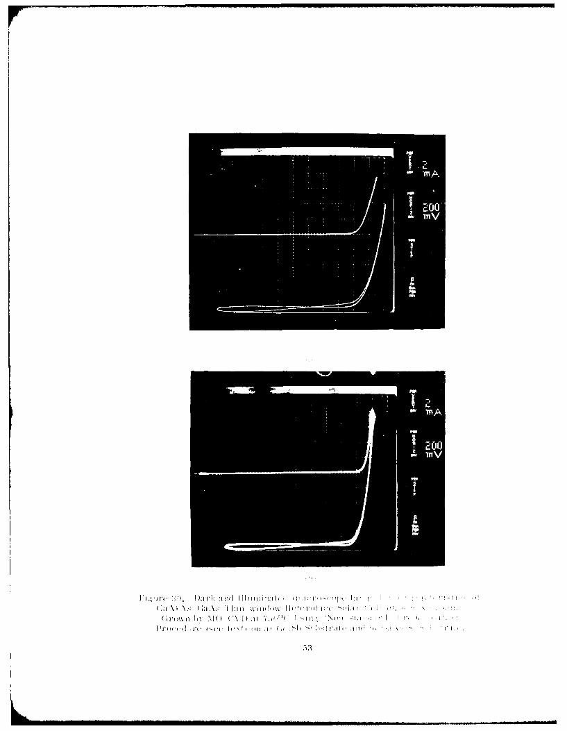
I ~ ~ ~ ~ ( ('VII~i~ I) T.i i iI
..~ .........
Figure 31. Dark and Illuminated (microscope lamp) I-V Characteristics ofGaAfAs-GaAs Thin-window Heteroface Solar Cell (0. 5cm x 0. 5cm)
Grown by MO-CVD at 7500C on Ge:Slb Substrate UsingStandard Predepos ition Procedure
cell Arva =0.25 _2
Inpot P,-,t - i 5 cm
5, 0..452
Figure '32. Dark and Illuminated (AIMO simulator. -135 mw,,cm 2 l-\*Chariacteristics of Another GaAf As -GaAs Thin-window
Ileteroface Solar (Cell (0. 5cm x 0. 5cm) Fabricatedon Samle Ge:Sh Substrate as Cell of Figure 31
54
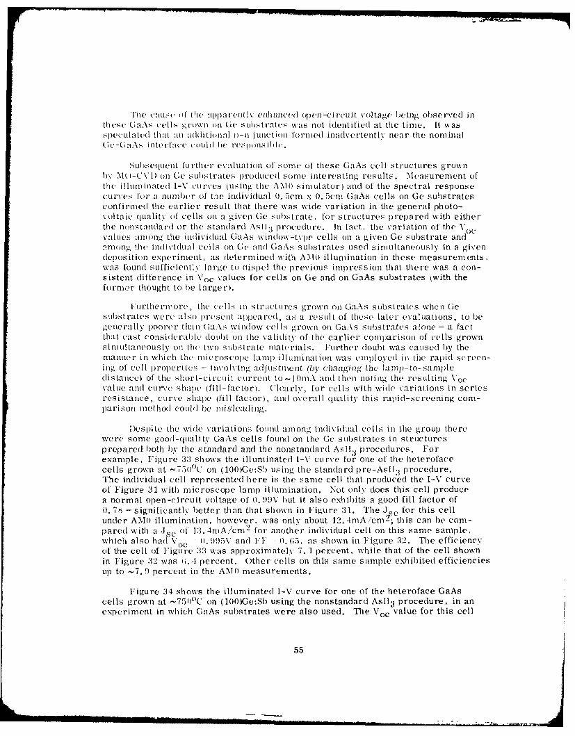
The cause odthe appret(11 enhanced open-circuit voltage being observed inthese GaAs cell s g-on on Ge subst1rates was not identified at the time. It wasspeculated that an additional 0-11 junction formed inadvertently near the nominalGe-GaAs inte rfLIce could hC responsil,
,-ubsequent further evaluation of some ol these GaAs cell structures grownbY M(U-'V1) on Ge substrates produced some interesting results. Measurement ofthe illuminated I-V curves (using the AMO simulator) and of the spectral responsecurves for a numl)er of the individual 0. 5cm x 0. 5cm GaAs cells on Ge substratesconfirmed the earlier result that there was wide variation in the general photo-voltaic qualitv of cells on a given Ge substrate, for structures prepared with eitherthe nonstandard or the standard As !13 procedure. In fact the variation of the Voc,values among tile individual GaAs window-type cells on a given Ge substrate andamong the individual cells on Ge and GaAs substrates used simultaneously in a givendeposition experiment, as determined with AM o illumination in these measurements,was found sufficiently large to cdispel the previous impression that there was a con-sistent difference in Voc values for cells on Ge and on GaAs substrates twith theformer thought to i)e large r.
lurthermore, the cells in structures grown on GaAs substrates when Gesubstrates were also present appeared, as a result of these later evaluations, to be1generally )oorer than Ga.\s window cells grown onl Ga_..s substrates alone - a factthat cast considerahle doubt on the validity of the earlier comparison of cells grownSinlultaneously on the two substrate materials. Further (loubt was caused by themanner in which the microscope lam 1) illunlination was employed in the rapid screen-ing of cell properties - involving adjustment (by changing the lamp-to-sampledistancel of the short-circuit current to10mA and then noting the resulting Vocvalue and curve shape (fill-factor). Clearly, for cells with wide variations in seriesresistance, curve shape (fill factor), and overall quality this rapid-screening com-parison method couad be misleading.
Despite the wide variations found among individual cells in the group therewere some good-quality GaAs cells found on the Ge substrates in structuresprepared both by the standard and the nonstandard Asl. 3 procedures. Forexample, Figure 33 shows the illuminated I-V curve for one of the heterofacecells grown at ~75 0°C on (100)Ge:Sb) using the standard pre-AslI 3 procedure.The individual cell represented here is the same cell that produced the I-V curveof Figure 31 with microscope lamp illumination. Not only does this cell producea normal open-circuit voltage of 0. 99V but it also exhibits a good fill factor of0. 7s - significantly better than that shown in Figure 31. The J3s for this cellunder AM0 illumination, however, was only about 12. ,tmA/cn this can be com-pared with a Jsc of 13. -ImA/cm2 for another individual cell on this same sample,which also had Voc (). 995V and IT 0. G5, as shown in Figure 32. The efficiencyof the cell of Figure 33 was approximately 7. 1 percent, while that of the cell shownin Figure 32 was G. 4 percent. Other cells on this same sample exhibited efficienciesup to -7.9 percent in the AM 0 measurements.
Figure 34 shows the illuminated I-V curve for one of the heteroface GaAscells grown at -750 0 C on (100)Ge:Sh using the nonstandard Aslt 3 procedure, in anexperiment in which GaAs substrates were also used. The Voc value for this cell
55
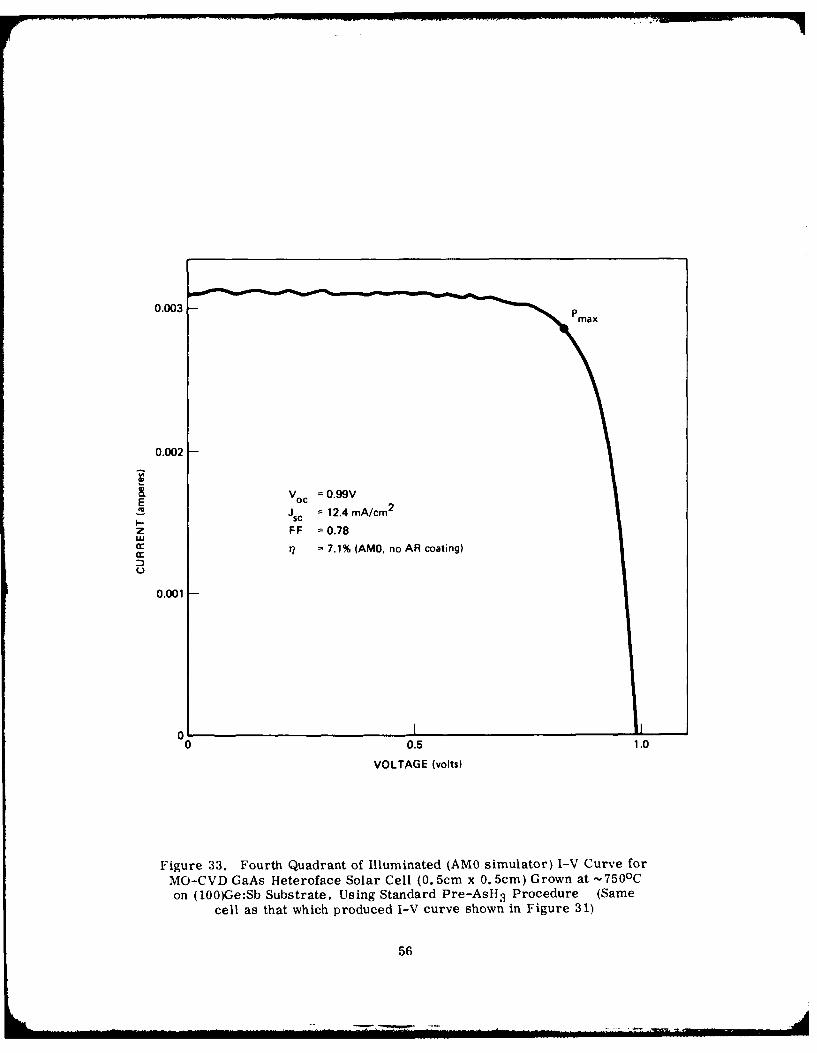
0.003 -Pa
0.002
V ~0.99VE OC
S12.4 mnA/cmn2
z FF = 0.78W
cr 77 = 7.1% (AMO, no AR coating)
0.001
00 0.5 1.0
VOLTAGE (volts)
Figure 33. Fourth Quadrant of Illuminated (AMO simulator) I-V Curve forMO-CVD GaAs Heteroface Solar Cell (0. 5cm x 0. 5cm) Grown at -750 0 Con (100)Ge:Sb Substrate, Using Standard Pre-AsH3 Procedure (Same
cell as that which produced I-V curve shown in Figure 31)
56
0.004
0.003
E
Z 0.002
0.001 V = 0.97V V000 16.7 mA/cm2
FF =0.71
=j 8.5% (AMO. no AR coating)
0 0.2 0.4 0.6 0.8 1.0
VOLTAGE (volts)
Figure 34. Fourth Quadrant of Illuminated (AM0 simulator) I-V Curvefor MO-CVD GaAs lleteroface Solar Cell (0. 5cm x 0.5cm) Grown
at -750 0 C on (100)Ge:Sb Substrate Using NonstandardPre-Asll 3 Procedure
is 0.97V, Jsc - 16. 7mA/cm 2 , the fill factor is 0.71, and the efficiency -8.5 percentfor AM0. The cell used to produce the I-V curve of Figure 30a, in which it hadappeared that an unusually large Voc had been generated by the microscope lampillumination, was on this same sample and was found in these later AM0 measure-ments to produce a very low Voc of only 0. 76V, a Jsc of 9. 7mA/cm 2 , a fill factorof 0. 70, and a power conversion efficiency of -3. 9 percent. Other cells on thissample had efficiencies up to 9. 8 percent in the AM0 measurements.
In most instances the cause of the relatively low efficiencies was obviouslythe lower-than-expected photoctirrent collected, indicating needed improvementsin cell design -- primarily layer thicknesses and doping concentrations - and apossible problem with minority carrier diffusion lengths due to defects in the GaAslayers grown on the Ge substrates. The later nmasurements, however, did notindicate a clear-cut preicrence for either the standard or the nonstandard Aslt3procedure for growing G(aAs heteroface cells on Ge substrates.
The spectral response measuremetts made on these GaAs Ge cells alsoindicated a lack of any long-wavelength response attributable to a possible secondbarrier involving Ge, except for two individual cells for which a very low Voc(0. 1 to 0. 28%'1 was found and some long-wavelength response was detected. It isbelieved that the GaAs cell was completely penetrated by the contacts in the process-ing in these instances, so that either a GaAs-Ge heterojunction or a Ge Schottkv-barrier cell resulted.
57
.. . . . . ." . . . . . . . I I I - - - .. . . oL, ,
'he possibilit v of obtaining improved GaAs cell performance om Ge Substratesby growth at reduced tV ,n1Iiera tires was briefly explored by growth of a GaAs heterofacecell structure at 660oC on a (100 Ge: Sb substrate; the substrate had been coated onthe back with sputtered Si().) about (00A thick, as in previous experinients with Gesubstrates. The individual 0. 5cin x 0. 5cm cells processed on this sam ple exhibitedgenerally poor (lark and light I-V characteristics when examined with the microscopelamp and the probe contact, with considerable junction leakage evident and alsoevidence of excessive series resistance. When one of the cells was characterizedwith the AMO simulator this general behavior was again observed. Under thatillumination the Voc was found to be only 0. ,V , much lower than found for theother Ge-based cells described above (ef Figure :32). The observed Jsc was13. 2 mA 'cin 2 and the fill factor was very low. Thus, even though this cellStructure was p repared with the predeposition procedure that involved only verybrief exposure of the substrate to Asl. 3 before the TMG was admitted, it appearedthat other things occurre(l at temperatures as low as (;(;0°C to result in relativelypoor quality growth of the cell structure.
Late in the I hase I program, at about the time the above A.M0 measurementswere being ma(le on the GaAs 'Ge cells grown earlier, additional GaAs window-typccell structures were grown on Ge:Sb substrates at-700°(" and on GaAs:Si substratesat -750o( , with the standard pre-growth exposure for Asll3 being used in several ofthe experiments and the nonstandard procedure of very brief exl)osure to Asl;1 beingused in two of the runs. Figure 35 shows the spectral response curves for two ofthe heteroface cells of this group, one grown on GaAs and the other grown (in aseparate deposition experiment) on Ge. The junction depth (p-type GaAs layerthickness) in the two cells was intended, by selection of deposition l)arameters, tob)e nominally the same. The large difference in blue response in the two casessuggests a major difference in the minority carrier diffusion length in the GaAslayers on the two substrate materials.
Unfortunately, however, the overall results obtained with this group ofsamples were decidedly inferior to those discussed above. Problems encounteredin the functioning of the reactor system late in the Phase 1 program wereapparently adversely affecting the properties of this group of cell structures,irrespective of the substrate material being used. Additional experiments withMO-CVD GaAs cell structures on either GaAs substrates or Ge substrates werethus delayed until early in the Phase 2 program.
It is clear that the GaAs cells produced on Ge substrates by the MO-(_'VDprocess in the Phase 1 program were of much poorer quality than those formedon GaAs sul)strates. It is believed that the device processing techniques thatwere used may have been responsible for some of the adverse effect, but otherfactors were probably more influential. The SiC.) coating used on most of theGe substrates sh.)uld have prevented serious interaction of the sul)strate and theM(i-'VI) reactant atmosphere, although no attempt was made to evaluate criticallythe integrity of the Si()2 layer or to determine an optimum thickness ordeposition procedures.
Whereas clear evidence of a more defective GaAs-Ge interface region wasfound for structtres grown with the longer-duration standard (as opposed to the verybrief non-standard) exposure of the substrate to Asl 1 , somewhat less conclusiveresults were obtained for the photovoltaic performance of cells in the two
58
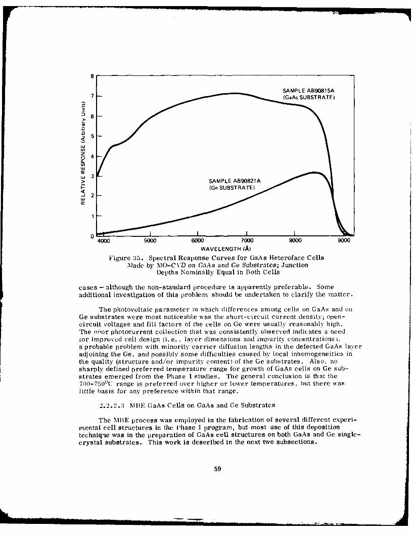
8
SAMPLE AB90815A7 (GaAs SUBSTRATE)
-5
Y)z0 4UL
cr
32
04000 5000 6000 7000 800 9000
WAVELENGTH (A)Figure :35. Spectral Response Curves for GaAs Heteroface Cells
Made by MO-CVD on GaAs and Ge Substrates; JunctionDepths Nominally Equal in Both Cells
cases - although the non-standard procedure is apparently preferable. Someadditional investigation of this problem should be undertaken to clarify the matter.
The photovoltaic parameter in which differences among cells on GaAs and onGe substrates were most noticeable was the short-circuit current density; open-circuit voltages and fill factors of the cells on Ge were usually reasonably high.The fnoor photocurrent collection that was consistently observed indicates a needtor improved cell design (i. e., layer dimensions and impurity concentrations),a probable problem with minority carrier diffusion lengths in the defected GaAs layeradjoining the Ge, and possibly some difficulties caused by local inhomogeneities inthe quality (structure and/or impurity content) of the Ge substrates. Also, nosharply defined preferred temperature range for growth of GaAs cells on Ge sub-strates emerged from the Phase 1 studies. The general conclusion is that the700-7500 C range is preferred over higher or lower temperatures, but there waslittle basis for any preference within that range.
2.2.2.3 MBE GaAs Cells on GaAs and Ge Substrates
The MIBE process was employed in the fabrication of several different experi-mental cell structures in the Phase 1 program, but most use of this depositiontechniq'mi was in the preparation of GaAs cell structures on both GaAs and Ge single-crystal substrates. This work is described in the next two subsections.
59
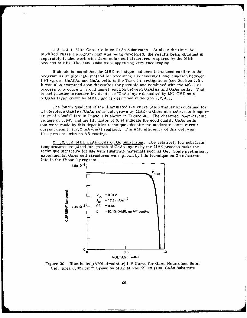
2.2.2.3.1 MBE GaAs Cells on GaAs Substrates. At about the time themodified Phase 1 program plan was being developed, the results being obtained inseparately funded work with GaAs solar cell structures prepared by the MBEprocess at EIRC Thousand Oaks were appearing very encouraging.
It should be noted that the MBF technique had been introduced earlier in theprogram as an alternate method for producing a connecting tunnel junction betweenLPE-grown GaAIAs and GaAs cells in the Task 5 investigations (see Section 2.5).It was also examined soon thereafter for possible use combined with the MO-CVDprocess to produce a hybrid tunnel junction between GaAIAs and GaAs cells. Thattunnel junction structure involved an n+GaAs layer deposited by MO-CVD on ap 'GaAs layer grown by MBE, and is described in Section 2. 2. 4. 1.
The fourth quadrant of the illuminated I-V curve (AM0 simulator) obtained fora heteroface GaAf As/GaAs solar cell grown by MBE on GaAs at a substrate temper-ature of -580 0 C late in Phase 1 is shown in Figure 36. The observed open-circuitvoltage of 0. 94V and the fill factor of 0. 84 indicate the good quality GaAs cellsthat were made by this deposition technique, despite the moderate short-circuitcurrent density (17.2 mA/cm 2 ) realized. The AMO efficiency of this cell was10. 1 percent, with no AR coating.
2.2. 2.3.2 MBE GaAs Cells on Ge Substrates. The relatively low substratetemperatures required for growth of GaAs layers by the MBE process make thetechnique attractive for use with substrate materials such as Ge. Some preliminaryexperimental GaAs cell structures were grown by this technique on Ge substrateslate in the Phase 1 program.
4.8x 10⁻⁴
Pmax
Voc = 0.94VE Jsc = 17.2 mA/cm2
.SSl 2.4x 10- 4 FF = 0.84zW 17 = 10.1% (AMOnoARcoating)
cccc
010 0.5 1.
VOLTAGE (volts)
Figure 36. Illuminated (AMO simulator) I-V Curve for GaAs Heteroface SolarCell (area 0. 025 cm 2 ) Grown by MBE at -580oC on (100) GaAs Substrate
60
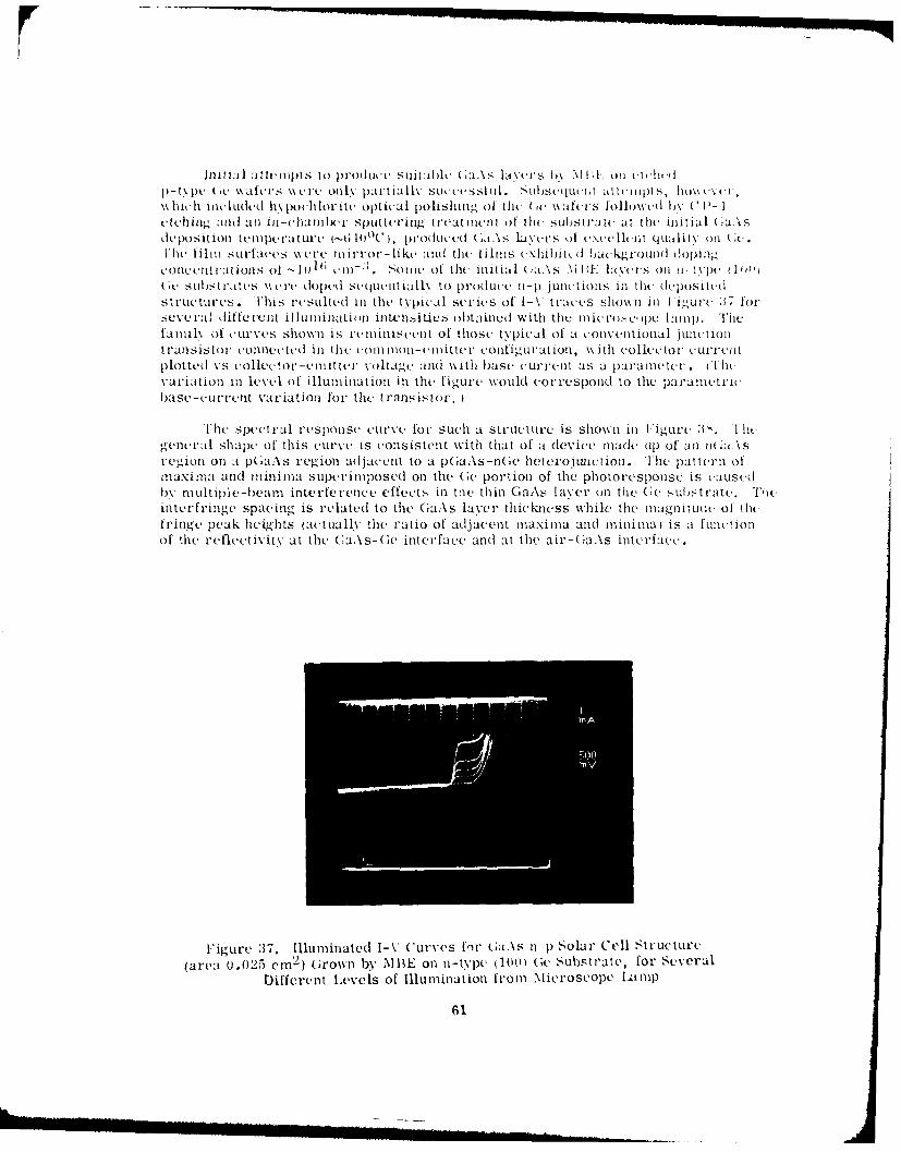
Ini Iia I a Itemn pts to produwc s u i~I abl (;m\\s lavuirs [\ \l I I, on cIth-dp -type ( Ge\ wair I \VS\ereIV(AI ot 1) 1pat IaI l k -51 4St itI. > 'III )St ( (I it at I (-IljI)1AS, Ito\\Vr,\\ [lieh inleIIN h1p04h LOP it(- Optical polis hinig of tile ('4 wi \k(I h)1hWs ((I% i\ 1( C Ietchn and an in-charuhet' sputtering tl'Vat utnt of the SUbS5trajV al the( initial (;U.\Sdeposit ion telpe a tare (-6 4OOk' , produceed (; layL ers Of e CCet li qtt:Ii t\ On l[Hit flln suirfaces \\t''Ill mirtor'- likc atnd the flmsi 1 xhiIlialtd IiackgFo~tnI doping'onlcenltrationlS of '- 111) LtMn:1 S olic of thle initial (14 a.s\ ilayers on li-type (I'(wt subhstrates dop Ield SeqIuclit all\ to I'rOd~tc 11-1) Juncetionts in dlt dlepositedlst ru(*tures. [h'is resdw siitIn the typical ser'ies of 1-0 t aces shoIXn in Figur n 0 7 forseverpal differient illum ination mW 5.-Aie5 4)btIilced with thilBi 4cipe Ialij. TheWAY OfIl lC LWeS shown is Pt'emiflisi.''It of those typial of a convntimofl jwulionranlsiS tor connec ted ill tilhe (4-Onmon1-ClIn itter PContigut'at ion, \ itholle OILtot curr'ent
plotted vs voilketot'- II ittet voltagu alai "ith base Lqw'rellt as a para mtr. P hevariation inl level Of1 i hu mat ion in thle f igure Would correspond to the pa ra metrtiebaSe -currenlt Variatiotl for thle tr,1IS is tor. I
Irhe spectral response curve [or stuch a strueture is shown1 in VigUre a ,. I hegeneral shlape' Of this eurve is ronsistet with that of a device made up of an ni a.\sregion on a pGaA s region wadjcn to a p(;aAs-n( e heterojuiiction. The pat tern ofmaXimla and milin a SUPerimlpose[ Onl thle Ge portion of the photoresponlse is caused[by rnLlt ille-[)eam intwerkrupnce effcts in the thin GaAs [Ayer (on tihe M; subst rate, Tleinterft'inge spac ing is relatedi to the Ga*%s lav ' r thickness ileIC thle lnag1nitudCo Of Ihefringe peak heights (aIctually thle ratio of adjacent maximia and mini mali is a fLUIliionof the ( fit tt ivity at the ('a.\ s-(k interface and at the ail -(a \s interiface
Figure 37, Illuminated [-V Curves fnr G;aAs ni p Solar Cell Stucture(area 01.025 em-) Grown by MI3E on n-type jiQol (k, Substrate, for Several
Different Levels of Illumination from Microscope LI-ip
61
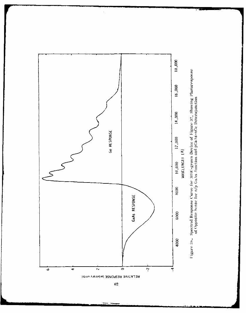
C)
Cd
0
C-
C)-
CC
0
C- 00C)
(slin Aiili~e) SN~d3U AIIV13-
62(
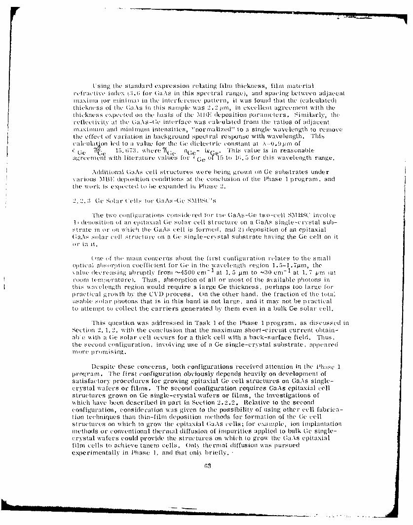
t'sing the standard expression relating film thickness, fihm materialrIractive ilidex (:,.(; for (Ga ,s in this spectral range), and spacing between adjacentMaxiMa O lo minimlla) in the interference pattern, it was found that the (Calculated)thickness of the aAs in this sample was 2.2 pm, in excellent agrec ment with thethickness cxp'cted on the hasis of the M [UK deposition paraneters. Similarly, thereflectivit% at the GaAs-Ge interface was calcuiated from the ratios of adjacentMaXillmll and llillillLMm intensities, 'normalized' to a single w\avelength to removethe effect of variation in background spectral response with wavelength. ThisCahulat on led to a value for the Ge dielectric constant at \ --0.9 pm ofe "e 15). (78, where ne n( - . This value is in reasonableaig reenient with literature V:lues for Ge of15 to 1G;. 5 for this wavelength range.
Additional GaAs cell structures were being grown on Ge substrates undervarious MB1 (eposition conditions at the conclusion of the Phase 1 program, andthe work is espccted to 6e expanded ih Phase 2.
2. 2. 3 Gie .olar Cells fm GaAs-Ge SMIlS("s
The two configurations conside'ed l r the GaAs-Ge two-cell SMIBSC involve1 deposition ot, an epitaxial Ge solar cell striUctu,'C on a GaAs single-crystal sub-strate in or un which the GaAs cell is formed, and 2) deposition of an epitaxialGaAs solar cell st ructuore on a Ge single-crYstal substrate having the Ge cell on itor in it.
(mne of tPb main concerns about the first conlfigu ration relates to the smalloptical ahsnrption coefficient for Ge in tile wavelcngth region 1.5-1.7pim, thevaluC dec reas ing ab ruptlV from -4500 cm - 1 at 1. 5 pm to -30 cm-1 at 1. 7 pm atroom temperatureL). Thus, absorption of all or most of the available photons inthis wvelength region would require a large Ge thickness, perhaps too lar'ge forpractical growth by tile CV) process. On the other hand, the fraction of the total
usable solar photons that is in this band is not large, and it may not be practicalto attempt to collect the carriers generated by them even in a bulk Ge solar cell.
This question was addressed in Task I of the Phase 1 program, as discussed inSection 2. 1.2, with the conclusion that the maximum short-circuit current obtain-abe with a Ge solar cell occurs for a thick cell with a back-surface field. Thus,the second configuration, involving use of a Ge single-crystal substrate, appearedmore )romising.
Despite these concerns, both configurations received attention in the P'hase 1program. The first configuration obviously depends heavily on development ofsatisfactory procedures for growing epitaxial Ge cell structures on GaAs single-crystal wafers or films. The second configuration requires GaAs epitaxial cellstructures grown on Ge single-crystal wafers or films, the investigations ofwhich have been described in part in Section 2.2.2. Relative to the secondconfiguration, consideration was given to the possibility of using other cell fabrica-tion techniques than thin-film deposition methods for formation of the Ge cellStructures on which to grow the epitaxial (;a.\s cells; for example, ion implantationmethods or conventional thermal diffusion of impurities applied to bulk Ge single-crystal wafers could provide the structures on which to grow the (aAs epitaxialfilm eells to achieve tanem cells. Onlv thermal diffusion was pursuedex)erimentallY in Phase 1, and that onlv briefly.
.3
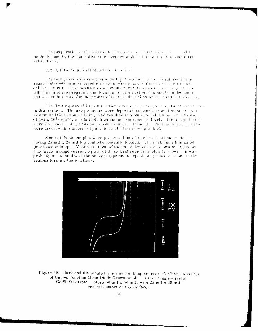
I.(~d -I t u I iutl i- I I&s-5Q 'I- It; Ii 4) I ' I j
S Li I S C Vt i I S
fft I l I liti h i th p1 c a n ra11 enipit Ili_ It I ~ I - st -itIil hiat I i n~ If I I- I .
an Iii -I tir II-et Iu th I I I I L1 s al d I .O g t 1'nd A f\2 .- s 'i t ?l - I(
Piet fi rst v.\ptIaxa11 1e p-ti 1 Llir't iti )I st I' -t Wt-t 0 1'( 1 1" 11 :> >1s- nt-
Wvee 'C t\W ii %\ ith laX 1 - t\ -*I - 1 III ti1 ir-k1 i li I !Ia :1 '- ) ii tI Ir
Som'e of these amlple> were i 'res- e ftl nt.) mil x .)o mtil ms- 1 lc-hav ing 25 mui x 25 nii tak p c'nntai-t-, renttiai I' II\I teUd. 111 & nII, :11)1] iti k U, iI(11i C rasop I aQ01C 1,1111)) 1-V \ rn ev lt fe atI 0Ie iC 111N devic he c ate In ti inl I-iuru t-
thie 1 ar2e leakage n uren t\'piAl,1 Of thle.- ti r:-t dev ire. Ls- ie a rk %Nh ,ii Itiaprobably asntteilted with the eu p-type and li-tilie2 pg HIt'L-ent:iiij.- it lewrc-ions forming" thle jnnctians
Figure 39. Iark and IllifuiatedI kfil ItiS('iil)( lanj1i1 stlilrtt' l--\ 1Aiarat'icris-'tirsof Ge p-n J1 UnCtion Mesa D io~j'k G rown 11 ) M.( - 11In Sil le-crvst a
Ge:Sh SubStratC iNlesa 30 mil \ 50 mil. %N ith 2.5 mil x 25 milcentrn cit ntiuct on top surufare i
64
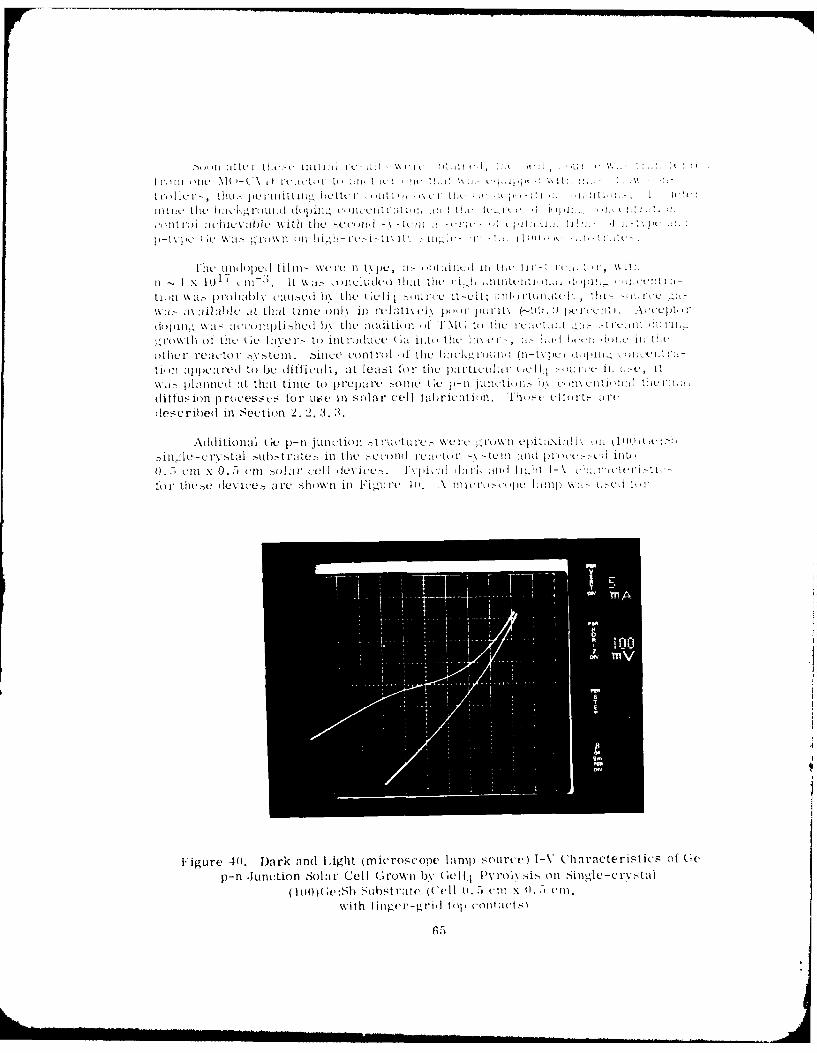
I CO )IL Ii Iv I ' i lt :il th1 1 it' ~ ,
L ,) -- , 1,l 11 1 It 1111 i:- 11 h1l~ ~ tLa tI F I Io It t .I pc I\ tat I
tIll ~ a.- he roI ll .( ~-Iu c Il, It2t ( I I' It t It'i -IIi~ it I IF Wl
Ia I a~Ilit. at11 that i e it InII I 'cll l pa I(l ' (-I. It Il C-tIt.....
1ti 1l X 101~~c 'e C 1to It i~ilt, k IIlea~t IIL tlc pa., dtu t p( -cIl I - ttt.
k a % pl a c at that tille to l p iean IIi% Ge p-, I jtIt lt h I\ Lni LI t: ~ t _\ lU.jj1
piltution pricssusl [- ue b\ tola cel NallatUI. 'tU :i itU't art- I V1
-,l )I I :c-W Ii t' 5 td t( ) b t dat if , f i n it It I C~ u 1 1 il r,1 IM 1- t o I t Ia(nd 1- - t e II t -C it
(I. JAIcItIx 0. a tllt .oLi ll t Octi., GQ ~I -il haG lth a tt i-t
ti1tt 1111 r(L'esc to[C -hu l ill( Inslar~tIt'[ cell I tialii> Tlu i tl ( IW:- :I- 1'' F
Figure 40.~ Dark and Light (microscope lamp souirce I I-V Characteristics of Ge
p-n -Junction Solar Cell Grown bv Gel, Pvt yroly si: onl sinJe-c rv stiat
10)(:sI Suibstratte (C'ell 0.5 co11 x 1. - cm1,with litigci'-gridtop1 cmOfl;itts
6 5
Ii IIIII I:t it tta ion. ( I i ) lk- c- Ie i H :i I t u L a I v I]' t IxhII I *I. iito tLhc IV I :ILii\ CI \ 11i41 lp ti Colil(VItt l tioll ill t1e 1) i tll 11 1 u i > ( j 1v I, 11 1 ..
Nt :111 of the ptxa (IC J~lictioll >tLtiutU IuV We iU V t I :It I(.' tI.; IuW d Owul]) hI-V cha racte ristius as sh~ w in I- iglrc i I If Wt er ,thet ir I(aC voltt (4 1 1 e
d Iiode Ics waIs ve- low I() k, as sh Io\\n , p)r obalI heuanSC' tl d ZI r aided I ut 00I])( I-' 10I2 N1%itheir than11 an1 abrupt ilnctioll.
Ill lthe >evenQlth Ilonth oh the 1pr0111raml tile ( ;L dIMpoztioni expu lililullt> ;oCFt
ran-lu 1rred fromt tile Nt )-(i\ I)leutor se to :Inlothulwl rl r -ur - lutoia
%%ai> comletelkL] lie of (',I andi A, ilnlAItiie antl Ll ed lo to that titttu, jll\ 1oW 1i
Iupo.sitionl expe limlnenis This wa- C\Ipuuted to Iredttre the haul-A tn dpIfl 0
-li aioll fotIltd ill thu ( e I ave 1'>b :1 >iinilr lt a ll)i t.
Hie, Iir t t;c int> iU~ll ti> veautol Wuru ilepo~itet on i ro di cinl l-t\ ju
(.1e >LihJ-tralte> obtained front C~~ePu o. :111d jxtli>-Ild h\It~~x l{ \. II.Xjet-illicltal g'rowth ()f undoped tilllt> at -Tj-OWt. oi tltte >htlt i lludhoth cillil.- :tIld >ub.trates thalt wtu found to ble enitirely p t\vpU. It \ I 0 ~pcutlthatL thc - e~> ee nIllfctation, od the therl.\ 10 p11-- (to) 1, t.j)U
lWOto or,-It I' inllh-eiiit%' 11-t\lle ( 'AL UXlto Uof to tep\a~ T I lo7L' t extendd peU rio( k . That 111i wa.> indeed thle ua .: u wa>- %e I iu. I i), oc u rI uxj r I -
Menunt> inl 1hi tile ( re ub t ra te( niate 11 :t N a> N \ CIeC I dCepo)- itU )1 Ittt I I oo. 1,1 1u>-
I- i t I reI Ii. f)nr k ;i IIi gh t tmi icr ('su op cI an I, s o ur e I-V Chara11- 1 sC I- I -
I III ti I IC ,:I ) )(Ic ;I w 1 k ( I I I, -II I :- )) "-ing Ic - 1\ :-I
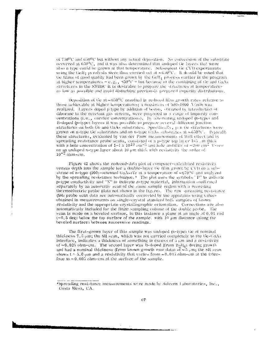
of 75oO 0 C an NOW 00 buit Withoit ala ac(tul (It dpo. iion. No Cll%1\ rlsiofl 0I thle s-ubst rateOLNCCI rd at 657, 0 C , and it w as Also detenri- nc I that urn I ped( 6k ikave r> that wvere
also tpecon d begrow ix at that teipe raLUre. )LuhCsjQlet (U (_V C I Xpel'imntL iing thle (AC11.1 pv ro lss We e thus carrtied (Alt at -650o(' 11 -ii ~ ould be noted that(We fims of good ciutalit ha ben grow n by thele II r j(Ces s earle intl
at higher tempe ratu re s - e. g. , S50o1 C -- but becau.n ()e l te o bnngof Ger and (;aAns~tru ctu res in the SAL BSU it is desrable to prcpa re the tcuctur i'.altnptau '.an Ion- as I)05sible and avoid disturbhing p revbmAu I p pared impurcity distcibutio ln
IDepo.-ition of (Ac at -(;50()(- resLted ill reduce~ II jun i, rot'lx rate:- relative tothose achiev able at highe r temnpe ratu res ; a l\in L\ll run 1,1001-1000 A 'ruin wkasrealized. I avers doped 1) type by addition oW horoni, ()btajneld h\ inti-odulction (Itdihorane to thle r'eaetant (a' tem ee erdi an II, cty OI
centrations (i.e. , carrier onweentrationn ly :dt emaing undoped (n-typei and1-doped (p- type [aye is it Was pOns ibIe to pVrep]re-e e Lral defcelit jun ctionrStitrcttires Oil both GQe and Ga-AsSLubst rates.- S)iiclI, p 11 Ge s7t lieto ret- Weregrown on n-type Ge ustae and on n-type (W~ rA ubwttc- at -65011'. l~pic aI lthese structures, evaluated by van der 10mv w masure bent> "1 10I ei'lect and byspreadtng resistalice probe scans , conlsinted () a p-type2 top lay er 1-5 In thickwith a hole correen ttio of 1-4 x 10¹⁹ cr-:, anid hole inobilIitv () -200 cr))On an Unduoped n-type laver about 10 p1 11x thick With rcnitiit thle order oi10-2 ohm-cm.
Figure 42 shows the reduced-data plot of Cornpo tee-Ca] tnlaI'tedre tvtversust1 depth into the sample for a double-I aye I GC film gr1own byVD I onl a subO-strate of n-type (100)-oriented GaAsa:e at a temperaturre of -6700C and analyzedby the spreading resistance techniqute. *The plot us-es the symbols ' '" to indicatep-type conductivity atnd -N" to indicabo n-type atral, irforrmat ion confirmedseparately by an automatic scan of the Same Sample region wilh a re"cording"-thermoelectric probe (data not shown in the figu re I. The raw-peain resistanlce(SR) probe scan data are automatical ly CorrectedI by tnt app~laratus using value>-obtained in InfeaSU renienth on sirgle-crystal standard bul!L samples of knownresistivity and the npproprite cryvstallographic orientation. Corrections are alsnoautomaticaily included for the finite sainpling voltime of thle dloule probxe. Thescan is made on a beveled sotrface, in this instance a plane at an anigle of 0.01 cadi-0. 5 degi below the top surface of the sample, wth 10 pm distance kalong thebeveled surface) between Successive reatdings.
The first-grown ly\er of ths sale was undoped (n1-type) Gec of nxominlalthickness 7. 5 paLn; the SR scani, which was not carried completely to the Oe-tGaAsinte rface, indicates a thickness of something in exeess of 5 1an and a renistivitvof 0.025 ohm-cm. Thle second layer was Ibl-dped (fromn "2110 duvinlg gr owthand had a nominal thickness (from known growth rate dlata) of 5 pm; the SRscanshows t -5.0 pVm and a resistivity that varies from -0.015 ohm-em :U the inter-face to -0.005 ohm-en at th strfnee of the sample.
*Spxreading resistanee uMean I VC fie nts we ir' in I by Solecon I aboratorne s' Inc.,Costa Alesa, CA.
P NO4~,t t$N,4 a4 i S-EP
-- _ _- P i
PL
-30,0 2.0 4.0 6.0 8.0 ]0,0
DEPTH INTO SAMPLE (lim)
(Probe load 10g; bevel angle 0.01 rad; step increment 1%;m)
Fihrure 42. Resintivity as Function of l)epth into Sample as Obtained by SpreadingResistance Probe 6can on Beveled Sut'fa-Ce in "i'o-layer CVI) Ge Film Grown
at 650°C on n--type GaAs Surface; p-n Junction Shown Is at Interfacebetwveen p-type and n-type Ge I.ayers
Similar nieauremunts on the (_ic CVD) layers grown on high-resistivity n-typeGC subStrntes confirmed the therma|l conversion to p type of that substrate materialwhen the filmn was depo;:3ted at 75)C' but its remiainingr n type when th_, film wasdeposit.ed at 650-660"C. T1he Sit technique wa-s found to be a useful method ofnmeasuremnent for certain types of ., aiple that are not conducive to other techniquesof conductivity,-type dectermnination or t t'ansp~ort property measurement.
]'he as-rrown (Ge layer .-,Ilrjace on ,one of these su nples were not very.s mooth and reflective, as if the (100)- orie nted sulb 7trate growth surfaces hadbeen improperly cleaned or somehow contatminated after placement in the deposi-tion chamber. "Ihis applied to films on bothi Ge arod Ga.As substrates. Conse-(luuntly, the sub,,trate cleaning procedures were carefully reviewed, the reactorsystemn was checked thorougly~ for leaks, and a brief examination of the effectsof" substrate crystallographic orientation was made to attempt to identify the cause,,f the relatively poor surface quality.
le cleaning p)rocedures were judged adequate and no s'ys tern leaks v eret, ,,ind. flo~ke,er, when a (1 lil-oriented Ge substrate was included along with theI-,i-irien'.ed (;e substrate in one of the experiments, the resulting Ge layer on theIl I iibstrate %, as relatively smooth and highly reflective, and for a measured
ti.,centration of I1 x 100 cm-3 exhibitedI a hole mobility of 1G85 em2!/V-see.
68
~ J4~?~4I
SIDEPTHIIITOlllllIII(Im)(.ro.eIlod ==I;mbvelmaIgl 0.0 rad ste inreen .10_ : -m)
over twice as high as any obtained in similarly doped p-type laYers at any timeearlier in the program.
It thus appeared that the pyrolysis process used for growing p-n junctionstructures in Ge by CVD was capable of producing material with properties adequatefor solar cells. However, even at deposition temperatures as low as 650 0 C the rmaltype conversion of the 8-10 ohm-cm substrates was found to occur occasionally,depending primarily on the length of the deposition experiment. It was also foundthat Ge deposition in this lower temperature range often resulted in layers thatwere quite mottled in appearance for growth on both (100)Ge and (100)GaAs sub-strates, as if some contaminant had remained on the substrate surface prior tothe deposition and despite the careful cle-ntng procedures used. Reducing thedeposition rate (to ~500 A/min) by decreasing the reactant concentrationsimproved the general appearance and the surface morphology of the film *o someextent.
The photovoltaic performance of some of the Ge solar cell structures madeby these CVID techniques was evaluated. The cell structures were grown on n-typesingle-crystal substrates of (100)Ge:Sb and (100)GaAs:Te. The p-type Ge layerswere B-doped (from B2116 ) and typically 1-5 1 im thick; the n-type layers wereundo ed and typically -7 pjm thick. This group of structures had been grown at-680 C by Gell 4 pyrolysis in 112.
The composite wafers were processed either into 50 mil x 50 mil mesadiodes, with 25 mil x 25 mil top contacts, or into the conventional arrays of0.5 cm x 0.5 cm individual cells using the standard solar cell contact patternpreviously described. In-Au was used for the p-type contacts and Sb-Au-Ni forthe n-type contacts.
The dark and illuminated I-V curves of a typical 50 mil x 50 mil Ge mesadiode grown on a GaAs substrate are shown in'Figure 43. Under the illuminationof the microscope lamp the I-V curve shifted as shown, and the Isc is ~20 pA.The p-type Ge layer of this sample was -5 Lm thick.
The I-V curves for one of the 0. 5 cm x 0.5 cm Ge cells grown on a Ge sub-strate are shown in Figure 44. This cell structure had a B-doped p-type Ge layer1 Lm thick on the n-type Ge substrate. The Ge deposition rate for this sample wasslower than that of the structure represented in Figure 43. Large leakage currentsare evident in both cells.
Fortunately, n-type Ge substrates of much lower resistivity (-0.03 ohm-cmlbecame available at that time and they were then used for the subsequent Ge deposi-tion experiments. This allowed deposition temperatures of up to -750 0 C to be usedand this change immediately led to the growth of clean, smooth and highly reflectiveGe films on both Ge and GaAs substrates. Measured electron mobilities(van der Mauw method) in the films also increased, from -:300 cm 2 /V-sec forundoped n-type films grown at 650 0 C to ~400 cm 2 /V-sec for fibns grown at 750(T(electron concentration -3 x 1018 cm-: 3 in each case).
69
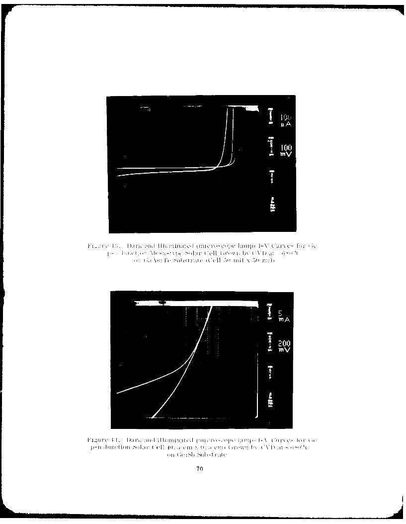
F [- L Irc 1:;. D l ri, 111, I I I I I I I I) I I It C, 1 1, 111 C I', L )I) I I I I) U F\ (2
;,-.1 lilt tl')!l ' ,Ihr Cell b\ ('\I) I,, i; - AI - -I I bs I I t t ( I
V IL u rc I I I :ill, i I I Ill ill in:11 o I Ill I n k.()l ;I till I I r\ c -
: l I
70
Lm
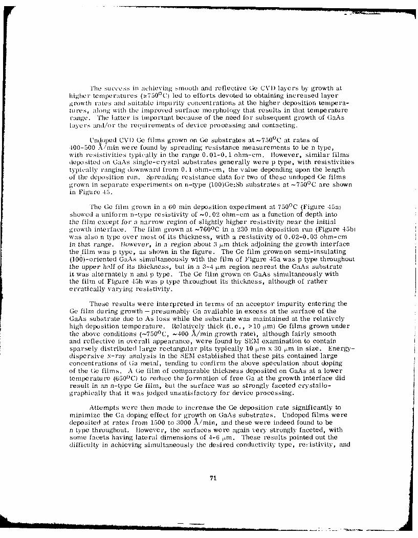
The su.ce.s., in achieving smooth and reflective Ge CVI\') layers by growth athigher temperatures (27500C) led to efforts devoted to obtaining increased layergrowth rates and suitable impurity concentrations at the higher deposition tempera-tures, along with the improved surface morphology that results in that temperaturerange. The latter is important because of the need for subsequent growth of GaAslayers and/or the requirements of device processing and contacting.
Undoped CVI) Ge films grown on Ge substrates at -750°C at rates of-100-500 X/min were found by spreading resistance measurements to be n type,with resistivities typically in the range 0.01-0.1 ohmr-cm. However, similar filmsdeposited on Ga -s single-crystal substrates generally were p type, with resistivitiestypically ranging downward from 0. 1 ohm-cm, the value depending upon the lengthof the deposition run. Spreading resistance data for two of these undoped Ge filmsgrown in separate experiments on n-type (100)Ge:Sb substrates at -7500C are shownin Figure -5.
The Ge film grown in a 60 min deposition experiment at 7500C (Figure 45a)showed a uniform n-type resistivity of -0. 02 ohm-cm as a function of depth intothe film except for a narrow region of slightly higher resistivity near the initialgrowth interface. The film grown at -760 0 C in a 230 min deposition run (Figure 45b)was also n type over most of its thickness, with a resistivity of 0.02-0.03 ohm-cmin that range. flowever, in a region about 3 [m thick adjoining the growth interfacethe film was p type, as shown in the figure. The Ge film grownon semi-insulating(100)-oriented GaAs simultaneously with the film of Figure 45a was p type throughoutthe upper hqlf of its thickness, but in a 3-4 1im region nearest the GaAs substrateit was alternately n and p type. The Ge film grown on GaAs simultaneously withthe film of Figure -15b was p type throughout its thickness, although of rathererratically varying resistivity.
These results were interpreted in terms of an acceptor impurity entering theGe film during growth - presumably Ga available in excess at the surface of theGaAs substrate due to As loss while the substrate was maintained at the relativelyhigh deposition temperature. Relatively thick (i.e., 10 Im) Ge films grown underthe above conditions (-7500C, ~-400 A/min growth rate), although fairly smoothand reflective in overall appearance, were found by SEM exanination to containsparsely distributed large rectangular pits typically 10 Im x 30 .Im in size. Energy-dispersive x-ray analysis in the SEA] established that these pits contained largeconcentrations of Ga metal, tending to confirm the above speculation about dopingof the Ge films. A Ge film of comparable thiclkess deposited on GaAs at a lowertemperature (6500C) to reduce the formation of free Ga at the growth interface didresult in an n-type Ge film, but the surface was so strongly faceted crystallo-graphically that it was judged unsatisfactory for device processing.
Attempts were then made to increase the Ge deposition rate significantly tominimize the Ga doping effect for growth on GaAs substrates. Undoped films weredeposited at rates from 1500 to 3000 A/min, and these were indeed found to ben type throughout. However, the surfaces were again very strongly faceted, withsome facets having lateral dimensions of 4-6 im. These results pointed out thedifficulty in achieving simultaneously the desired conductivity type, resistivity, and
71
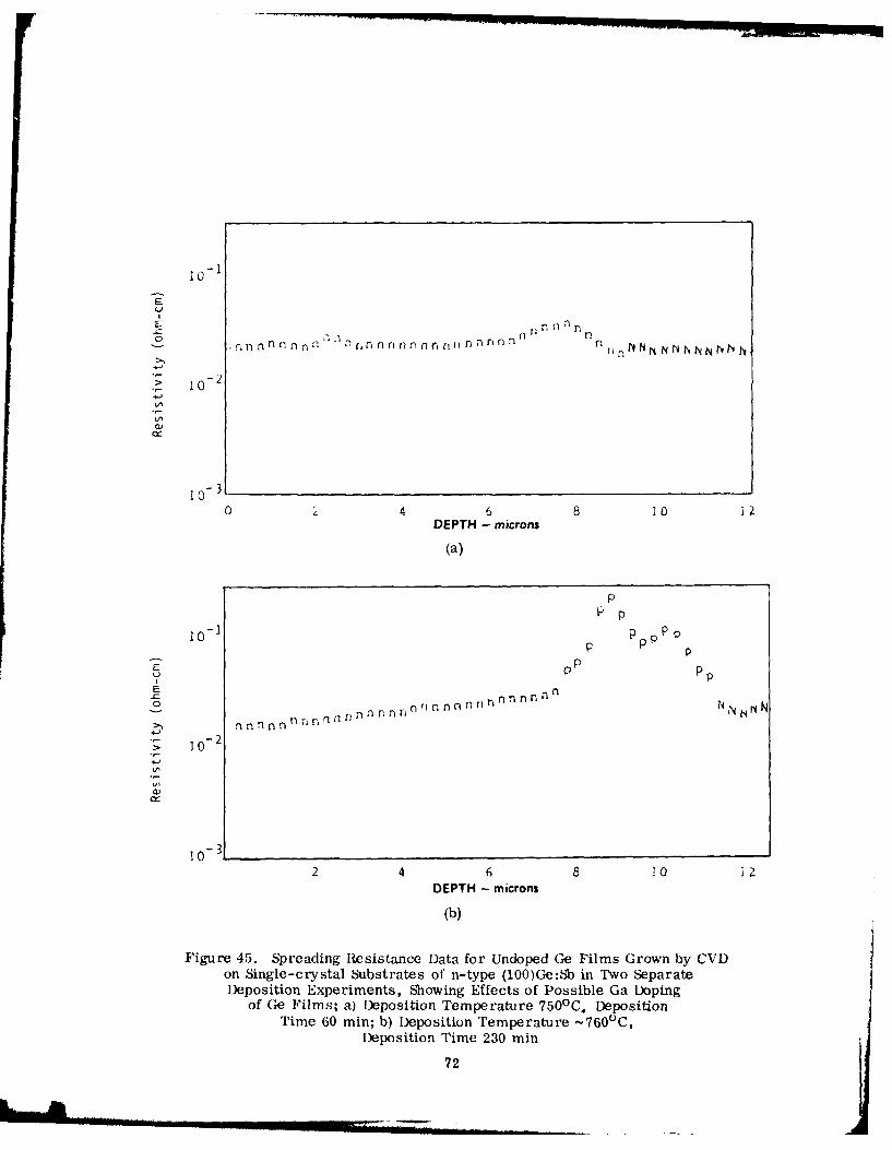
io- I
E
o fl " n, nnn!nn (INN N N N N NN
> - 2
S 10-4--
,
o 6 10DEPTH - microns
(a)
P p
p P" I -I p p
E P
30- 2F
o n n l n., N N J
F.10 - 234--,
2 4 6 10DEPTH - microns
(b)
Figure 45. Spreading Rlesistance Data for Undoped Ge Films Grown by CVDon Single-crystal Substrates of n-type (100)Ge:Sb in Two SeparateDeposition Experiments, Showing Effects of Possible Ga Doping
of Ge Films; a) Deposition Temperature 7500 C. DepositionTime 60 min; b) Deposition Temperature -760(C,
Deposition Time 230 min
72
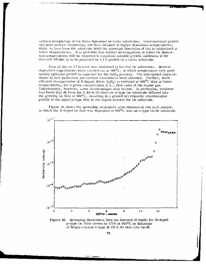
surlace morphology in Ge tilms deposited on GaL.s substrates. Good epitaLxial growthand good surface morl)hology are best obtained at higher deposition temperatures,while As loss from the substrate (with the attendant liberation of Ga) is minimized atloweri temperatures. It is probable that further investigations at lower Ge deposi-tion temperatures will be required to establish suitable growth conditions if thetwo-cell SMBSC is to be prepared by CVI) growth on a GaAs substrate.
Most of the Ge CVI) work thus continued to involve Ge substrates. Severaldeposition experiments were carried out at S00°C, at which temperature very goodquality epitLxial growth is expected for the GeIl 4 process. The anticipated improve-ments in film perfection and surface smoothness were obtained. Further, moreefficient incorporation of 13 dopant (from B2116) is realized at 800°C than at lowertemperatures, for a given concentration (i.e., flow rate) of the dopant gas.Unfortunately, however, some disadvantages also accrue. In particular, evidencewas found that Sb from the 0.02-0.03 ohm-cm n-type Ge substrate diffused intothe growing Ge film at 6001C, resulting in a graded net impurity concentrationprofile in the doped p-type film in ihe region nearest the Ge substrate.
Figure 46 shows the spreading resistance scan obtained on one such sample,in which the B-doped Ge film was deposited at 800 0 C onto an n-type Ge:Sb substrate
:2
.02 P
0 p|pPP0 ppp.
:0-3
pPP
aa _p ppppppp ppppppppppppl
;0- 4 pppppppPpptaPP
:0- 5 1
u 4 6 8 10 12DEPTH - miacv
Figure 46. Spreading Resistance Data (as function of depth) for B-dopedp-type Ge Film Grown by CVD at 800 0 C on Substrateof Single-crystal n-type (0.02-0.03 ohm-cm) Ge:Sb
73
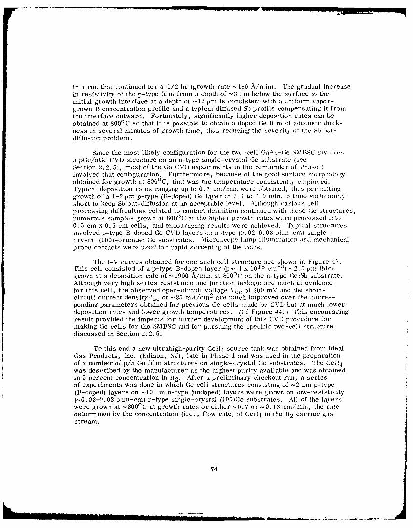
in a run that continued for 4-1/2 hr (growth rate -. 180 A/niin). The gradual increasein resistivity of the p-type film from a depth of -3 1am below the surface to theinitial growth interface at a depth of -12 jm is consistent with a uniform vapor-grown B concentration profile and a typical diffused Sb profile compensating it fromthe interface outward. Fortunately, significantly higher deposition rates can beobtained at 800 0 C so that it is possible to obtain a doped Ge film of adequate Lhick-ness in several minutes of growth time, thus reducing the severity of the Sb ,ut-diffusion problem.
Since the most likely configuration for the two-cell GaAs-Ge S.MBSC involve.a pGe/nGe CVD structure on an n-type single-crystal Ge substrate (seeSection 2.2.5), most of the Ge CVD experiments in the remainder of Phase 1involved that configuration. Furthermore, because of the good surface morpholo*'obtained for growth at 800 0 C, that was the temperature consistently employed.Typical deposition rates ranging up to 0.7 Lm/min were obtained, thus permittinggrowth of a 1-2 im p-type (B-doped) Ge layer in 1.4 to 2. 9 min, a time sufficientlyshort to keep Sb out-diffusion at an acceptable level. Although various cellprocessing difficulties related to contact definition continued with these Ge structures,numerous samples grown at 800 0 C at the higher growth rates were processed into0.5 cm x 0.5 cm cellsi and encouraging results were achieved. Typical structuresinvolved p-type B-doped Ge CVD layers on n-type (0.02-0.03 ohm-cm) single-crystal (100)-oriented Ge substrates. Microscope lamp illumination and mechanicalprobe contacts were used for rapid screening of the cells.
The I-V curves obtained for one such cell structure are shown in Figure 47.This cell consisted of a p-type B-doped layer (pn- -lx 1018 cm - 3 ) - 2.5 ),m thickgrown at a deposition rate of - 1900 A/min at 800 0 C on the n-type Ge:Sb substrate.Although very high series resistance and junction leakage are much in evidencefor this cell, the observed open-circuit voltage Voc of 200 mV and the short-circuit current densityJsc of -35 mA/cm 2 are much improved over the corres-ponding parameters obtained for previous Ge cells made by CVD but at much lowerdeposition rates and lower growth temperatures. (Cf Figure 44. ) This encouragingresult provided the impetus for further development of this CVD procedure formaking Ge cells for the SIBSC and for pursuing the specific two-cell structurediscussed in Section 2.2.5.
To this end a new ultrahigh-purity GelI 4 source tank was obtained from IdealGas Products, Inc. (Edison, NJ), late in Phase 1 and was used in the preparationof a number of p/n Ge film structures on single-crystal Ge substrates. The Ge1 4was described by the manufacturer as the highest purity available and was obtainedin 5 percent concentration in 112. After a preliminary checkout run, a seriesof experiments was done in which Ge cell structures consisting of -2 im p-type(B-doped) layers on -10 1Lm n-type (undoped) layers were grown on low-resistivity(-0.02-0.03 ohm-cm) n-type single-crystal (100)Ge substrates. All of the layerswere grown at -800 0 C at growth rates or either -0.7 or'-0.13 ilm/min, the ratedetermined by the concentration (i.e., flow rate) of Gelt 4 in the 112 carrier gasstream.
74
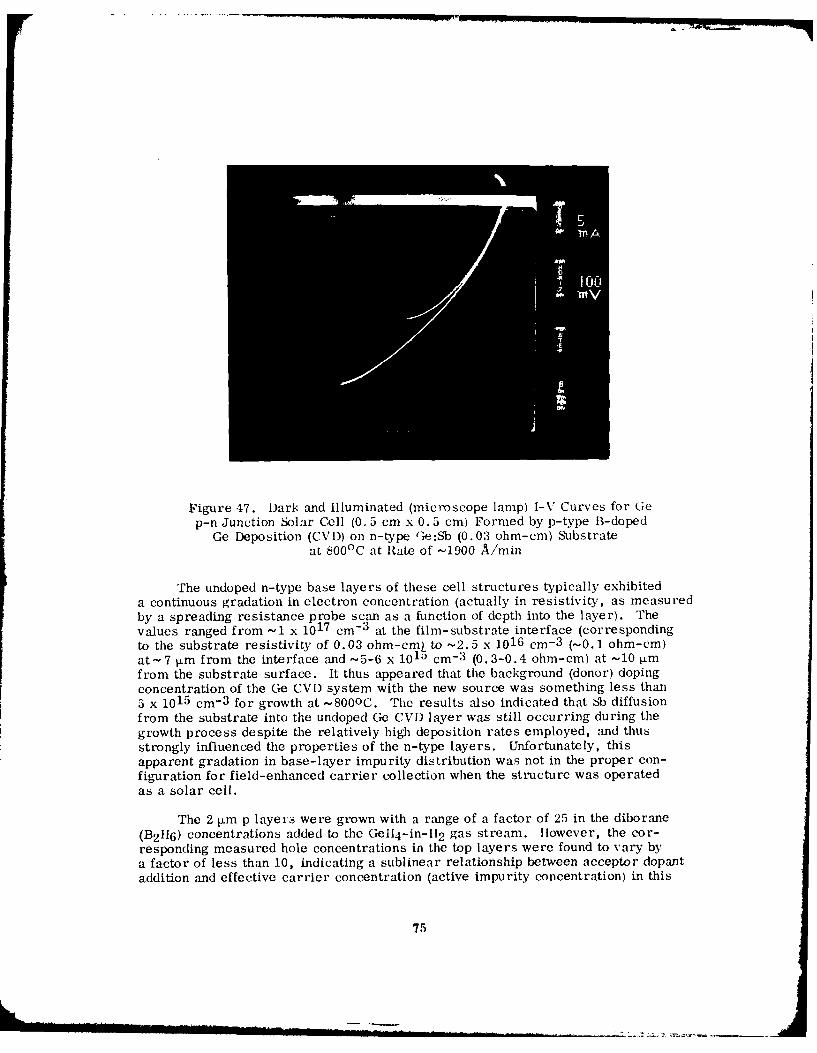
Figure 47. Dark and Illuminated (microscope lamp) I-V Curves for Gep-n Junction Solar Cell (0.5 cm x 0.5 cm) Formed by p-type B-doped
Ge Deposition (CVD) on n-type Ge:Sb (0.03 ohm-cm) Substrateat 800 0 C at Rate of -1900 A/min
The undoped n-type base layers of these cell structures typically exhibiteda continuous gradation in electron concentration (actually in resistivity, as measuredby a spreading resistance probe scan as a function of depth into the layer). Thevalues ranged from -1 x 1017 cm - 3 at the film-substrate interface (correspondingto the substrate resistivity of 0.03 ohm-cmj to -2.5 x 1016 cm- 3 (-0. 1 ohm-cm)
at-7 Lm from the interface and -5-6 x 1010 cm- 3 (0.3-0.4 ohm-cm) at -10 Imfrom the substrate surface. It thus appeared that the background (donor) dopingconcentration of the Ge CVD system with the new source was something less than5 x 1015 cm- 3 for growth at N800oC. The results also indicated that bb diffusionfrom the substrate into the undoped Ge CVD layer was still occurring during thegrowth process despite the relatively high deposition rates employed, and thus
strongly influenced the properties of the n-type layers. Unfortunately, thisapparent gradation in base-layer impurity distribution was not in the proper con-figuration for field-enhanced carrier collection when the structure was operatedas a solar cell.
The 2 im p layers were grown with a range of a factor of 25 in the diborane
(B 2 116) concentrations added to the Gel14 -in-11 2 gas stream. However, the cor-responding measured hole concentrations in the top layers were found to vary by
a factor of less than 10, indicating a sublinear relationship between acceptor dopant
addition and effective carrier concentration (active impurity concentration) in this
75
[)pcrating rangeC. Spreading resistance scXnS on several of the structures indicatedthat the 2 jiLn p layers had regions probably about 0.5 jni thick at the junction inwhich there was significant reduction in the net hole (and thus the net B impurity)concentration. This could have been the result of continued diffusion of the Sb(or other unidentified donor) from the n layer and substrate, although the observedeffect might also have been an artifact of the method of measurement related toprobe size and the various corrections involved in the spreading resistancetechnique.
Several of the Ge cell structures were processed into 1.6 mm x 1.6 mmmesa-type cell arrays at Thousand Oaks, using nominally the same processingsequence as was used earlier in preparing 0. 5 cm x 0.5 cm Ge solar cells atAnaheim. These cells, along with several others processed at the same time insamples that had been grown earlier using the original (lower purity) Ge]14 sourcematerial, were characterized by dark and illuminated I-V measurements andspectral photoresponse measurements. Table 4 lists the principal depositionparameters, materials properties, and device characteristics of a number of thesecells.
The principal distinction between these small-mesa cells and those fabricatedearlier in the 0. 5 cm x 0.5 cm size is that the smaller cells were characterizedwith unalloyed contacts. De to unidentified difficulties in the contact alloyingprocedure, the alloying resulted in severely degraded cell performance whereas,of course, just the opposite effect should occur. The problem is illustrated forGe cell samples 73 and 79 in the table, where measurements are given for bothunalloyed and alloyed contacts. In both cases significantly lower Voc, Jsc, andfill factor values were found after the alloying procedure, which consisted ofheating the sample at 4000C in 112 for 2 min.
In general, the Voc values obtained for simulated AMO illumination with thesecells were lower than desired; open-circuit voltages of 250 mV or more should beachievable with Ge cells having good junction characteristics. llowever, as theabove discussion of Ge layer growth indicates, the junction properties were knownto be less than optimum in these structures - including those in which the activejunction was formed at the interface between a deposited p layer and an n-typesubstrate wafer. The largest Voc value observed for these cells - about 190 mV -should probably be viewed as acceptable for the junction quality represented. Itseems certain that modifications could be readil3 introduced into the layer growthprocedure to improve this parameter.
The maximum possible light-generated short-circuit current density thatcould be expected for Ge under AMO illumination, with no reflection losses and100 percent collection efficiency, is in the neighborhood of 75 mA/cm 2 . (The cor-responding value for Si cells is -55 mA/cm 2 . ) Short-circuit current densitiesas high as 33 mA/cm 2 were obtained with these Ge cells, about .41 percent of thetheoretical maximum. This is almost the same fraction of the maximum possiblephotogenerated current density as that often seen in production-model Si solar cellsthat are not optimized for maximum short-wavelength performance, and thus appearsrelatively good. In fact, most of the tabulated Jsc values exceed 25 mA/cm 2 , areasonable Jse in view of the deficient infrared output of the ElI lamps used in the
76
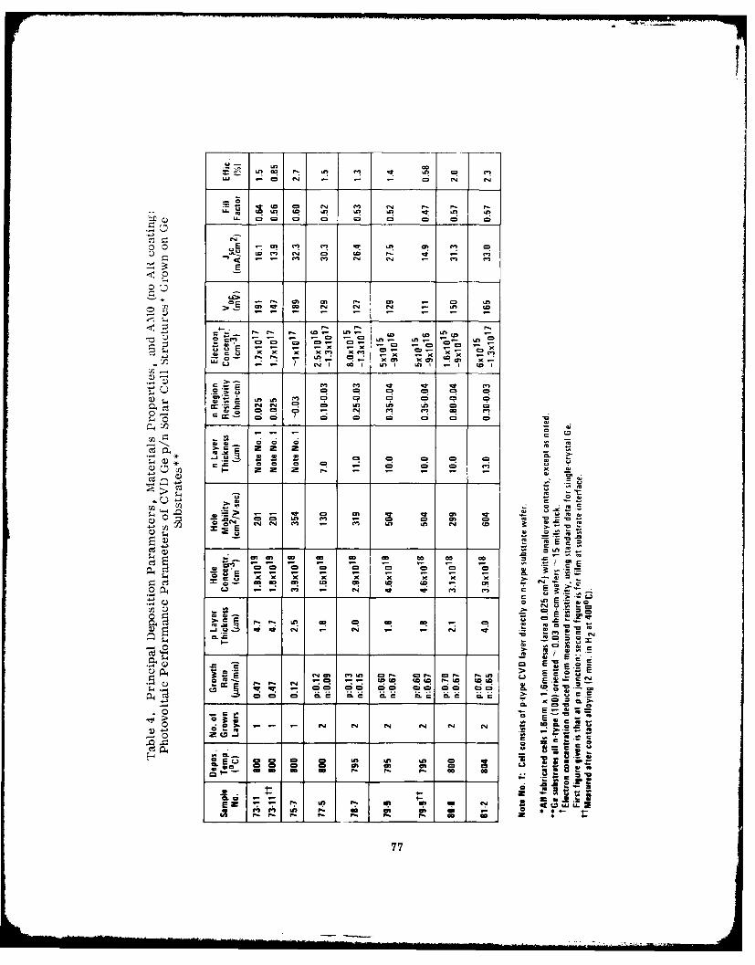
N~ UD r4
~0 N - - 0 N
L 0 NR C' Nr Nr NLic2 c2 c2 c= cD U, m
o 0 c7 0i 0i 0c a0 0
N= (
7; -cm -2 -. cR t2N
<p ____m n
c-_ n Nn qfl -T -c -
0 -R ER
Pz .= c-xa m qQ- -i NI gn, U - I
Q) z z
0 0 0
UU
U; N 4 , , U
> -D -" -
T -"14~~~ 0rn m 4 n r4 L
N N x~ - Cx 5, U, N C
0~~~) -1 Nen e
mml . za 0oCD Ca -
42~ C. 7- Ew E
> -
-" 0n I- - N L r
w~ E 2
.0 - E_ _ -.
ca j0- c
a. E c cm I
23 N U, 1 @ ~ DI I N 4 wu.c*~~ 4-01c
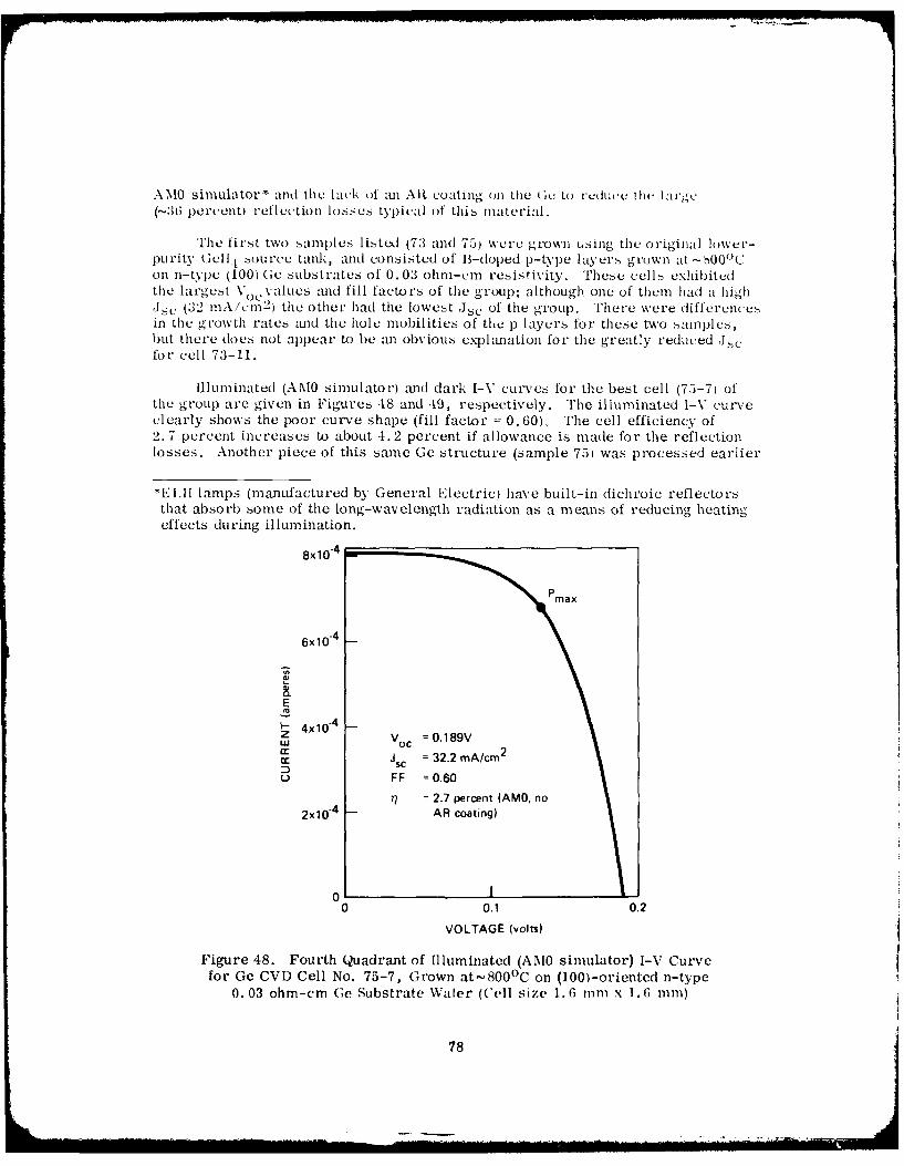
A MO simllator* and the lack of an Alt coating (i the ic to rCdUC-C til 1glr'-(-36 percent) reflection losses tyl)ical of this material.
'Fhe first two sallples listed (73 and 75) were grown using the original lowel-purity Gel lt source tanl, and consisted of B-doped p-type lay ers grown at - -00°Con n-type (100) Ge substrates of 0.03 ohm-cm resistivity. These cell. exhibitedthe largest V values and fill factors of the group; although one of them had a highJ.c (32 mA/em >2 ) the other had the lowest Jsc of the group. There were differencesin the growth rates and the hole mobilities of the p layers for these two sallples,but there does not appear to be an obvious explanation for the greatly reduced Jcfor cell 73-11.
illuminated (AIMO simulator) and dark I-V curves for the best cell (75-7) ofthe group are given in Figures -18 and 49, respectively. The illuminated I-V curveclearly shows the poor curve shape (fill factor = 0.60), The cell efficiency of2.7 percent increases to about 4.2 percent if allowance is made for the reflectionlosses. Another piece of this saine Ge structure (sample 75) was processed earlier
*EI.11 lamps (manufactured by General Electric) have built-in dichroic reflectors
that absorb some of the long-wavelength radiation as a means of reducing heatingeffects during illumination.
8x10 "
Pmax
6x10⁴
E
- 4 x 10 -4 --,, Vo 0. 189V
W VScc- Jsc = 32.2 mnA/cm 2
FF = 0.60
17 = 2.7 percent (AMO, no
2x10 "4 AR coating)
0
0 0.1 0.2
VOLTAGE (volts)
Figure 48. Fourth Quadrant of Illuminated (AAI0 simulator) I-V Curvefor Ge CVD Cell No. 75-7, Grown at-8000 C on (100)-oriented n-type
0. 03 ohm-cm Ge Substrate Waler (Cell size 1.6 mm x 1.6 mm)
78
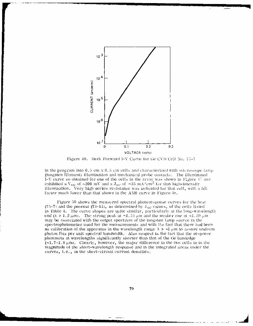
103
E0 5
Z -L"Cr"
106
0 0.1 0.2 0.3
VOLTAGE (volts)
Figutre -9. Dark Forward I-V Curve for" Ge CVD Cell No. 75-7T
in the ptogrtaml into 0. 5 cm x 0. 5 cm ceill. ald ch)aracterized with nicroscope lamp11(tunsten filamnt) illumination anod fiehai ca] probe Contat.. The illuminated-% curve so ottained for one of the cells in the array was shown in Figuire I7 Lnd
exhibited a Voc of ~200 im\ anod a 0Jsc of -3 5 l.\/n2 for that high-intensityillumination. \,'ry high series resistance was indicated for th-t ell, with a fillfactor much lower than that shown in the A .10 C~U 'e inl F.igure .8
Figrre 50 shows the measured spectral photorespone curve,. for the best(75 -7) anod the porest (73-11), as determined 1) N J3se values, of the cells listedin 'fable 4. Trhe curve shapes are quite similar, par'tiularly at the I on -wa\v e llgth
end (k > 1. 2 jm . The strong pea] at -1l. 54 p-m n md the wed, cer one at 1. 39 tlli
may be associated with the output speCtIIIII Of the tllgtstenl la-mp1 Source in thespectrophotometer used for the measurements and w ith tL~e fat that there had beenno calibration of the apparatuls in the wavelength rmeX > 1 -Lil to assure uniformphoton flux per unit spectral ban~dwidth. Also suspect is the fact that the responseplummeits at wavelengths significatly shorter than that of the Ge bandedge(1. 7-1. 8 lm). Clearly, however, the major difference in the two cells ill in) themagnitude of the short-wavelengthi response anrd in the integrated areas under theures, i.e. , in the short-circuit current densities.
"79
6..
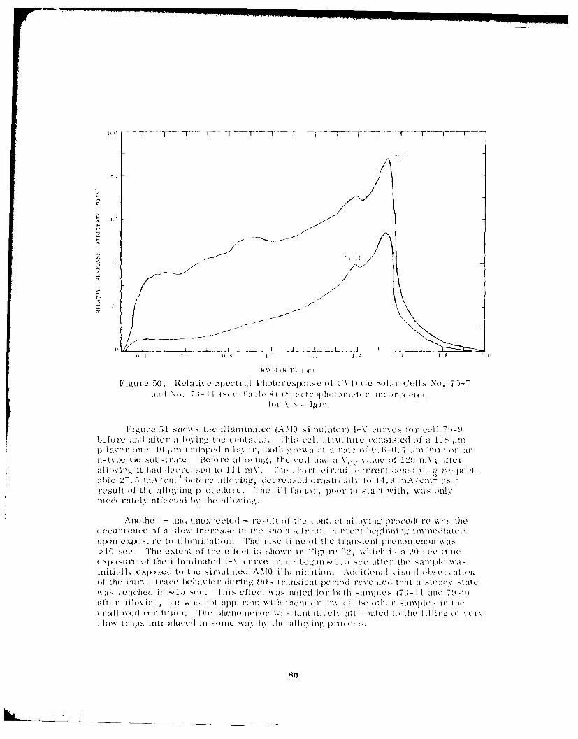
IdU - _T I- I- _ r-VTi- F-rT
0
1 0u141
Fii-u rv 50. Rtelative Spect ral Jlhotoce.sponsu of CVI) ki d)Ani Cut s No. 7--iiid No. 7-11 I sce Tfable 41 (Spet'utthotollicter 11w(oPP('('t(*
lFi-tire 51 show-,,s the illtumnated (AAIO SiMLuIJatAu' P -V \cu~r\Ce for' ('ell
tbefore andI after a1 Io\ inl- the ca )ntacts. This cell StrPuctu re colilistei of I I. llP) laver oil a 10 pn~ unidopedI fl aver, both grown at a raite of 0. 6-0.7 , min on anl
n-y c( GC -AtbtI'atQ. Bea re AloNvinll, the cel h ad a \ V atue of' 129 mnV ; atte rallo vI'ing it had dcr u a S', to II 111 mV. thu (1 dI0t-CIFPu (it cur' runt (ilZst iP Ie-pcu t -
able 27. 5 mA'urn hu.1112tvilg dL'crt'a.sd dras tical to ]4. 9 mA/CMn as areUSUlt of thu allyig 'rCudu ru . 'TIIu till fa uU t) I , ])(()P to starlt With, was" onl1Vmiode ratetv ifte Itedt by thu :il , vng.
A nrih1 r1 an L~UIC utelt - re sIll t of thue iOnltat a]10 ll". trIg 0PcedlC :u a thueoccur P'enice of a slo1w inicru aSC inl hUI SIIONrt-UcirClit rAIl Prunt tlegilFill" il jun ediatulvulmnf ex)OSU ru to ill u ni itiln . Thu r-isu, t in'ru of thu tralnsient phe nlomlenlon was,>10 ,u u Thu eXtent (If the Cffe ut is sllhownil Fi g.u u 2,which is a1 20 sCC t il"u0Xp s.u Pu of thue ill u n mallted t- V Curve trPace begul n0. -,cuc After thue samltu wainlitially expo 5ed U) thle Siutl ated ANMO ill ulmiatill). Akditid \ l~aiSvLu :l Obse P\ at 'iIIof the Curve trcebehavior P (n ing" tis t ralrsierlt pernid ruvualud thuI a s tuald \ ,t ateWas ruachud inl 15 Te.'his uffceut wsnoted for 110th sa~ls(7;1-11 anld 7 !Afte r a by jug, bu(t Was nlto lart With themI oP an'1 of thue Iltil smIllu ill t11Cunal loved condition). '11e tlhemlomtran wstentatiVel1 ;Itt' ihUtud to) thLe filli) Ofg at Vslow% trap's introIdu(ed ill smeWa\ b. IYtath Alaying tprluu .s>
80
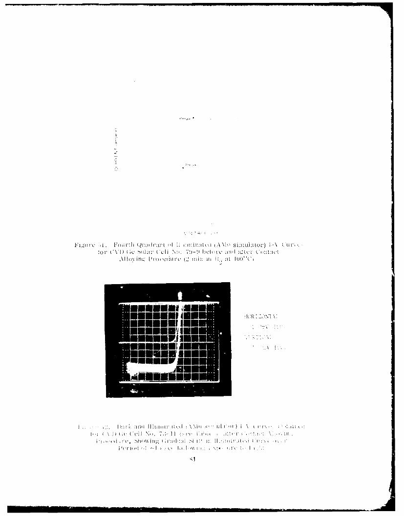
vTA
Fi1u~ "1 1.V O i t ItI QuiLItd ':ult oA lI i it It I {A I( sim1Ulto) I-\ ~ n
tor LW) I ic Solar Cell No,. hc-9r itud IC WtI' tniLtuwt
Al lo>' 102 Proceutire (2 mill i11 1 :it loU Ct,

j. AD-AIRS 764 ROCKWELL INTERNATIONAL ANAHEIM CA ELECTRONICS RESEAR--ETC F/A 10/2DEVELOPMENT OF HIGH-EFFICIENCY STACKED MULTIPLE-RANOGAP SOLAR C--ETC(U)OCT 80 R P RUTH, J S HARRIS, P D DAPKUS F33615-78-C 2036
UNCLASSIFIED C78-1225.28/501 AFWAL-TR-80-2096 NL
I n/////E/i//
SEmEIEEE//IA/EII-! iii i l/ ENmhIIIIIIIIl -
11111.0 .2 25236 IIWl
1111111IIII1 IIIlI '
MICROCOPY RESOLUTION TEST CHART
NATIONAL PRIM) OF ANDA[) 1 A
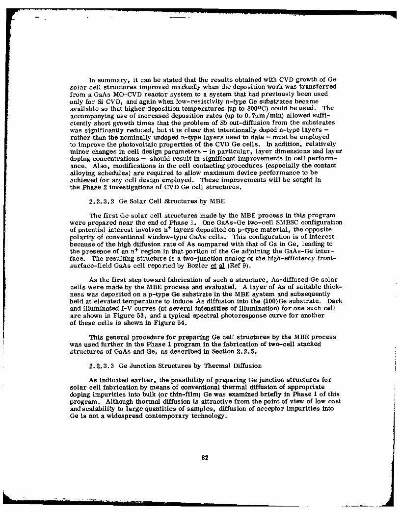
In summary, it can be stated that the results obtained with CVD growth of Gesolar cell structures improved markedly when the deposition work was transferredfrom a GaAs MO-CVD reactor system to a system that had previously been usedonly for Si CVD, and again when low-resistivity n-type Ge substrates becameavailable so that higher deposition temperatures (up to 8000C) could be used. Theaccompanying use of increased deposition rates (up to 0. 71im/min) allowed suffi-ciently short growth times that the problem of Sb out-diffusion from the substrateswas significantly reduced, but it is clear that intentionally doped n-type layers -rather than the nominally undoped n-type layers used to date - must be employedto improve the photovoltaic properties of the CVD Ge cells. In addition, relativelyminor changes in cell design parameters - in particular, layer dimensions and layerdoping concentrations - should result in significant improvements in cell perform-ance. Also, modifications in the cell contacting procedures (especially the contactalloying schedules) are required to allow maximum device performance to beachieved for any cell design employed. These improvements will be sought inthe Phase 2 investigations of CVD Ge cell structures.
2.2.3.2 Ge Solar Cell Structures by MBE
The first Ge solar cell structures made by the MBE process in this programwere prepared near the end of Phase 1. One GaAs-Ge two-cell SMBSC configurationof potential interest involves n+ layers deposited on p-type material, the oppositepolarity of conventional window-type GaAs cells. This configuration is of interestbecause of the high diffusion rate of As compared with that of Ga in Ge, leading tothe presence of an n+ region in that portion of the Ge adjoining the GaAs-Ge inter-face. The resulting structure is a two-junction analog of the high-efficiency front-surface-field GaAs cell reported by Bozler et al (Ref 9).
As the first step toward fabrication of such a structure, As-diffused Ge solarcells were made by the MBE process and evaluated. A layer of As of suitable thick-ness was deposited on a p-type Ge substrate in the MBE system and subsequentlyheld at elevated temperature to induce As diffusion into the (100)Ge substrate. Darkand illuminated I-V curves (at several intensities of illumination) for one such cellare shown in Figure 53, and a typical spectral photoresponse curve for anotherof these cells is shown in Figure 54.
This general procedure for preparing Ge cell structures by the MBE processwas used further in the Phase 1 program in the fabrication of two-cell stackedstructures of GaAs and Ge, as described in Section 2.2.5.
2.2.3.3 Ge Junction Structures by Thermal Diffusion
As indicated earlier, the possibility of preparing Ge junction structures forsolar cell fabrication by means of conventional thermal diffusion of appropriatedoping impurities into bulk (or thin-film) Ge was examined briefly in Phase 1 of thisprogram. Although thermal diffusion is attractive from the point of view of low costand scalability to large quantities of samples, diffusion of acceptor impurities intoGe is not a widespread contemporary technology.
82
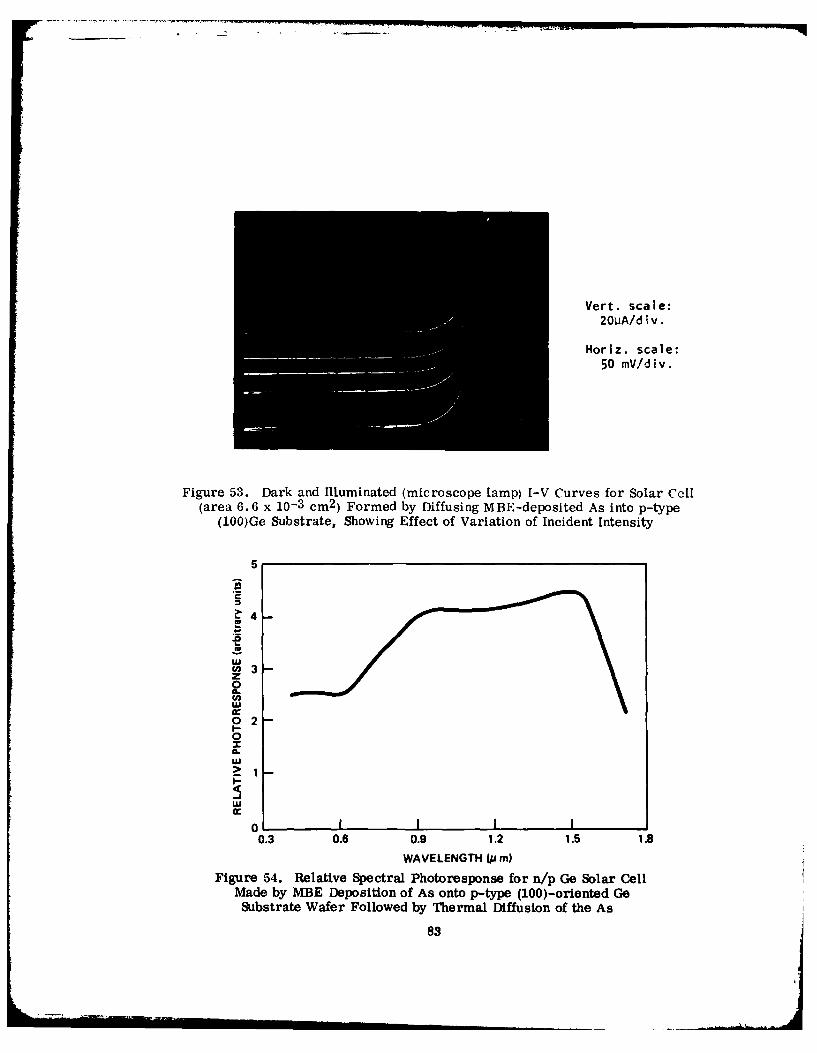
Vert. scale:.. =a.20ijA/d i v.
Horiz. scale:
50 mV/div.
Figure 53. Dark and Illuminated (microscope lamp) I-V Curves for Solar Cell(area 6. 6 x I0- 3 cm 2 ) Formed by Diffusing MBE-deposited As into p-type
(100)Ge Substrate, Showing Effect of Variation of Incident Intensity
5
.4
LU
0 3 -
z
U
0U,wIL
W0
0 I I0.3 0.6 0.9 1.2 1.5 1.8
WAVELENGTH (p m)
Figure 54. Relative Spectral Photoresponse for n/p Ge Solar CellMade by MBE Deposition of As onto p-type (100)-oriented Ge
Substrate Wafer Followed by Thermal Diffusion of the As
83
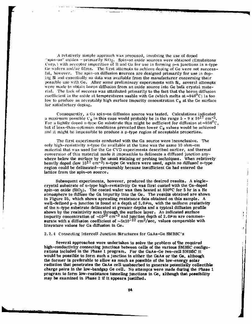
A relatively simple approach was proposed, involving the use of doped"spin-on" oxides - primarily Si0 2 . Spin-on oxide sources were obtained (EmulsitoneCorp.) with acceptor impurities of 13 and Ga for use in forming p-n junctions in n-typeGe wafers and/or films. The first attempts to achieve doping of Ge were not success-ful, however. The spin-on diffusion sources are designed primarily for use in dop-ing Si and essentially no data was available from the manufacturer concerning theirpossible use with Ge. After some preliminary experiments with Si, several attemptswere made to obtain boron diffusion from an oxide source into Ge bulk crystal mate-rial. The lack of success was attributed primarily to the fact that the boron diffusioncoefficient in the oxide at temperatures usable with Ge (which melts at -940 0 C) is toolow to produce an acceptably high surface impurity concentration Cs at the Ge surfacefor satisfactory doping.
Consequently, a Ga spin-on diffusion source was tested. Calculations indicateda maximum possible C s in this case would probably be in the range 5 - 9 x 1017 cm- 3 .For a lightly doped n-type Ge substrate this might be sufficient for diffusion at -850°C,but if less-than-optimum conditions prevailed then lower C s values would be achievedand it might be impossible to produce a p-type region of acceptable properties.
The first experiments conducted with the Ga source were inconclusive. Theonly high-resistivity n-type Ge available at the time was the same 10 ohm-cmmaterial that was used for the Ge CVD experiments described earlier, and thermalconversion of this material made it impossible to delineate a diffused junction any-where below the surface by the usual staining or probing techniques. When relativelyheavily doped (low 1017 cm- 3 ) n-type Ge wafers were used, again no diffused n-typeregion could be delineated--presumably because insufficient Ga had entered thelattice from the spin-on source.
Subsequent experiments, however, produced the desired results. A single-crystal substrate of n-type high-resistivity Ge was first coated with the Ga-dopedspin-on oxide (SiO2 ). The coated wafer was then heated at 8500C for 5 hr in a Heatmosphere to diffuse the Ga impurity into the Ge. The results obtained are shownin Figure 55, which shows spreading resistance data obtained on this sample. Awell-defined p-n junction is found at a depth of 2.01Am, with the uniform resistivityof the n-type substrate delineated at greater depths and a typical diffusion profileshown by the resistivity scan through the surface layer. An indicated surfaceimpurity concentration of _1020 cm - 3 and junction depth of 2.0Pr are commen-surate with a diffusion coefficient of -5x10 - 1 2 cm 2 /sec, values comparable withliterature values for Ga diffusion in Ge.
2.2.4 Connecting Intercell Junction Structures for GaAs-Ge SMBSC's
Several approaches were undertaken to solve the problem of the requiredhigh-conductivity connecting junctions between cells of the various SMBSC configu-rations included in the Phase 1 program. For the GaAs-Ge two-cell SMBSC itwould be possible to form such a junction In either the GaAs or the Ge, althoughthe former is preferable to allow as much as possible of the low-energy solarradiation that penetrates the GaAs cell unabsorbed to generate potentially collectiblecharge pairs in the low-bandgap Ge cell. No attempts were made during the Phase 1program to form low-resistance tunneling junctions in Ge, although that possibilitymay be examined in Phase 2 if it appears justified.
84
10 0 sNtINflh4HJ4 NN
P
p
P
IO-1 PP
I. P
Pp
10-3 P PP p
10 ppP
0 1 2 3 4 5 6
DEPTH - mi
Figure 55. Spreading Resistance Data for n-type Ge Single-crystalWafer with p-n Junction 2. 0 an Deep Formed by Diffusion of Ga at
850 0 C for 5 hr in He, Using Spin-on Oxide Diffusion Source
The formation of conducting junctions in GaAs received considerable attentionin the Phase 1 program, primarily by means of the MO-CVD technique but also byMBE methods. Although much of the work was done for the purpose of achievingconnecting junctions between GaAIAs and GaAs cells (Tasks 4 and 5, Sections 2.4and 2.5), all of the investigations of tunneling junctions in GaAs are describedhere.
2.2.4.1 GaAs Tunneling Junctions by MO-CVD
Early in the program a series of p+/n+ double-layer GaAs structures wasgrown by MO-CVD on both GaAs and Ge single-crystal substrates. These configu-rations were prepared for evaluation for possible use as the conducting tunneljunction between cells in the GaAs-Ge SMBSC. Zn and Se were used as the dopingImpurities for the p+ and n+ layers, respectively. Structures were grown at both700 and 7500C. Small-area mesa devices were formed for evaluation.
85
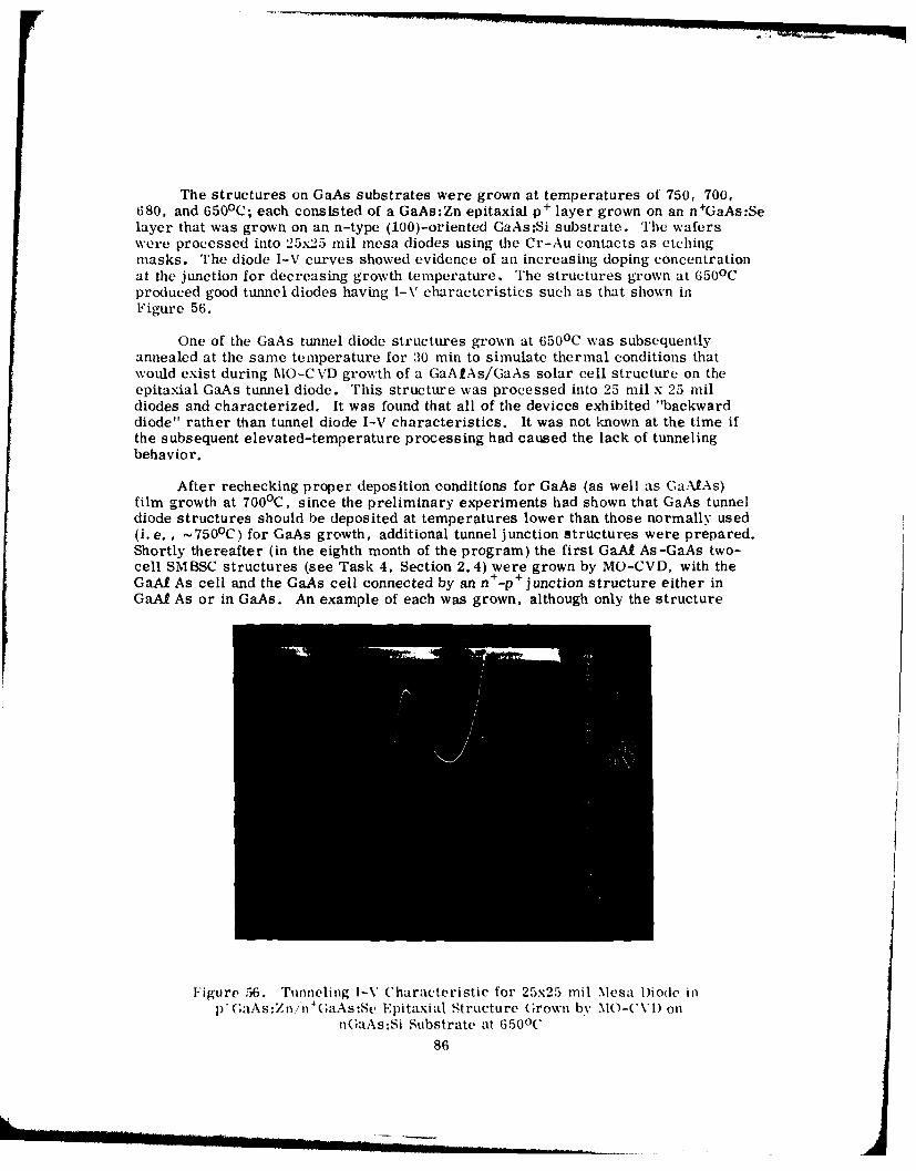
The structures on GaAs substrates were grown at temperatures of 750, 700,680, and 650°C; each consisted of a GaAs:Zn epitaxial p+ layer grown on an n+GaAs:Selayer that was grown on an n-type (100)-oriented GaAs:Si substrate. The waferswere processed into 25x25 mil mesa diodes using the Cr-Au contacts as etchingmasks. The diode I-V curves showed evidence of an increasing doping concentrationat the junction for decreasing growth temperature. The structures grown at 650 0 Cproduced good tunnel diodes having I-V characteristics such as that shown inFigure 56.
One of the GaAs tunnel diode structures grown at 650 0 C was subsequentlyannealed at the same temperature for 30 min to simulate thermal conditions thatwould exist during MO-C VD growth of a GaARAs/GaAs solar cell structure on theepitaxial GaAs tunnel diode. This structure was processed into 25 mil x 25 mildiodes and characterized. It was found that all of the devices exhibited "backwarddiode" rather than tunnel diode I-V characteristics. It was not known at the time ifthe subsequent elevated-temperature processing had caused the lack of tunnelingbehavior.
After rechecking proper deposition conditions for GaAs (as well as GaA.RAs)film growth at 700 0 C, since the preliminary experiments had shown that GaAs tunneldiode structures should be deposited at temperatures lower than those normally used(i.e., - 750 0 C) for GaAs growth, additional tunnel junction structures were prepared.Shortly thereafter (in the eighth month of the program) the first GaAf As-GaAs two-cell SMBSC structures (see Task 4, Section 2.4) were grown by MO-CVD, with theGaAf As cell and the GaAs cell connected by an n+-p+ junction structure either inGaAI As or in GaAs. An example of each was grown, although only the structure
Figure 56. Tunneling I-V Characteristic for 25x25 mil Mesa Diode inp'(;aAs:Zn/n 4 (;aAs:Se Epitaxial Structure Grown by MO-CVi) on
n(;aAs :Si Substrate at 6500 C86

with the connecting junction in the GaAs exhibited tunneling properties. Furtherdiscussion of the properties of those particular structures is given in Section 2. 4.
A subsequent group of tunnel junction structures was prepared at lower deposi-tion temperatures of 630 and 650 0 C, with n+/p+ structures consisting of(iaAs:Se/GaAs:Zn and p+/n+ structures consisting of GaAs:Zn/GaAs:Se. The n'/I ) 'devices were grown at both 630 and 650 0 C, and the layers were each -0.6 Pm thick.The samples were processed into mesa diodes of the customary dimensions (0.050 inx 0.050 in) and had the usual 0.025 in x 0.25 in Cr-Au contacts on the n + top layer.
I-V characteristics of two representative n+/p+ devices deposited at -650°Cand -630 0 C are shown in Figures 57 and 58, respectively. Diodes grown at 6500 Cshowed a weak tunneling current component in the characteristic, as seen inFigure 57. However, those grown at -630 0 C (Figure 58) exhibited almost a linearI-V curve, indicating that the doping concentrations on both sides of the junction wereso high that tunneling occurred even at bias voltages near zero. It can be seen fromFigure 58 that the device had a voltage drop of -0. 150V for a current density of-3A/cm 2 . This conductivity is more than adequate for a layer to be used as an inter-cell connection, so it appeared that the necessary parameters for joining the two cellsin this SMBSC structure could indeed be achieved by growth at relatively lowtemperatures--an important requirement. The extent to which these tunneling struc-tures would be consistently preserved during subsequent higher-temperature growthof GaAs and/or GaAf As cells in a tandem stack, however, remained to be established.
Figure 57. I-V Characteristic of GaAs:Se/GaAs:Zn n+/p + Tunnel JunctionStructure Grown by MO-CVD at -650 0 C on GaAs Single-crystal Substrate
(Mesa dimension 0.050 x 0. 050 in)
87
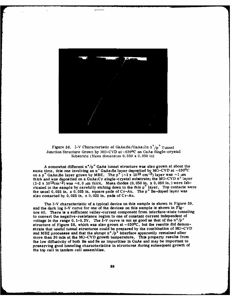
Figure 58. I-V Characteristic of GaAs:Se/GaAs:Zn n+/p + TunnelJunction Structure Grown by MO-CVD at -630 0 C on GaAs Single-crystal
Substrate (Mesa dimension 0.050 x 0. 050 in)
A somewhat different n+/p+ GaAs tunnel structure was also grown at about thesame time, this one involving an n+ GaAs:Se layer deposited by MO-CVD at -630 0 Con a p+ GaAs:Be layer grown by MBE. The p+ (-1 x 1019 cm- 3 ) layer was -1 Mthick and was deposited on a GaAs:Cr single-crystal substrate; the MO-CVD n+ layer(1-2 x 1019 cm- 3 ) was -6.0 m thick. Mesa diodes (0. 050 in. x 0. 050 in. ) were fab-ricated in the sample by carefully etching down to the thin p+ layer. Top contacts werethe usual 0. 025 in. x 0. 025 in. square pads of Cr-Au. The p+ Be-doped layer wasalso contacted by 0. 025 in. x 0. 025 in. pads of Cr-Au.
The I-V characteristic of a typical device on this sample is shown in Figure 59,and the dark log I-V curve for one of the devices on this sample is shown in Fig-ure 60. There is a sufficient valley-current component from interface-state tunnelingto convert the negative-resistance region to one of constant current independent ofvoltage in the range 0. 1-0. 2V. The I-V curve is not as good as that of the n+/p +
structure of Figure 58, which was also grown at - 630 0 C, but the results did demon-strate that useful tunnel structures could be prepared by the combination of MO-CVDand MBE processes and that the abrupt n+/p + interface apparently remained aftermore than 30 min at the MO-CVD growth temperature. This property results fromthe low diffusivity of both Be and Se as impurities in GaAs and may be important topreserving good tunneling characteristics in structures during subsequent growth ofthe top cell in tandem cell assemblies.
88
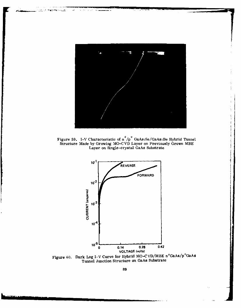
Figure 59. I-V Characteristic of n /p~ GaAs:Se/GaAs:Be Hybrid TunnelStructure Made by Growing MO-CVD Layer on Previously Grown MBE
Layer on Single-crystal GaAs Substrate
10-1
2
U
0 0.14 0.28 0.42VOLTAGE (volts)
Figure 60. Dark Log I-V Curve for Hybrid MO-C VD/MBE n+GaAs/p+GaAsTunnel Junction Structure on GaAs Substrate
89
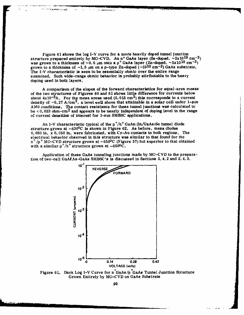
Figure 61 shows the log I-V curve for a more heavily doped tunnel Junctionstructure prepared entirely by MO-CVD. An n+ GaAs layer (Se-doped, -2x10 1 9 cm - 3 )was grown to a thickness of -0. 6 pm onto a p+ GaAs layer (Zn-doped, -5x1018 cm - 3 )grown to a thickness of -1. 5 lpm on a p-type Zn-doped (_1018 cm- 3 ) GaAs substrate.The I-V characteristic is seen to be essentially ohmic over the entire rangeexamined. Such wide-range ohmic behavior is probably attributable to the heavydoping used in both layers.
A comparison of the slopes of the forward characteristics for equal-area mesasof the two structures of Figures 60 and 61 shows little difference for currents belowabout 4x10- 3 A. For the mesa areas used (0. 015 cm 2 ) this corresponds to a currentdensity of -0.27 A/cm 2 , a level well above that attainable in a solar cell under 1-sunAMO conditions. The contact resistance for these tunnel junctions was calculated tobe < 0. 023 ohm-cm 2 and appears to be nearly independent of doping level in the rangeof current densities of interest for 1-sun SMBSC applications.
An I-V characteristic typical of the p+/n + GaAs:Zn/GaAs:Se tunnel diodestructure grown at -630 0 C is shown in Figure 62. As before, mesa diodes0. 050 in. x 0. 050 in. were fabricated, with Cr-Au contacts to both regions. Theelectrical behavior observed in this structure was similar to that found for then+ /p + MO-CVD structure grown at -650 0 C (Figure 57) but superior to that obtainedwith a similar p+/n+ structure grown at -650 0 C.
Application of these GaAs tunneling junctions made by MO-CVD to the prepara-tion of two-cell GaAIAs-GaAs SMBSC's is discussed in Sections 2.4.2 and 2.4.3.
10 "2 , .
10Iio
zw
10"4
0 0.14 0.28 0.42VOLTAGE (volts)
Figure 61. Dark Log I-V Curve for n+GaAs/p+GaAs Tunnel Junction StructureGrown Entirely by MO-CVD on GaAs Substrate
90
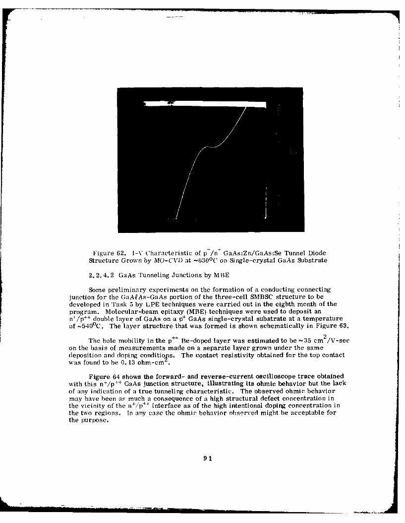
Figure 62. I-V Characteristic of p+/n GaAs:Zn/GaAs:Se Tunnel Diode
Structure Grown by MO-CVD at -6300 C on Single-crystal GaAs Substrate
2.2.4.2 GaAs Tunneling Junctions by MBE
Some preliminary experiments on the formation of a conducting connectingjunction for the GaARAs-GaAs portion of the three-cell SMBSC structure to bedeveloped in Task 5 by LPE techniques were carried out in the eighth month of theprogram. Molecular-beam epitaxy (MBE) techniques were used to deposit ann*/p 4 double layer of GaAs on a p+ GaAs single-crystal substrate at a temperatureof -540 0 C. The layer structure that was formed is shown schematically in Figure 63.
The hole mobility in the p++ Be-doped layer was estimated to be -35 cm 2/V-secon the basis of measurements made on a separate layer grown under the samedeposition and doping conditioF s. The contact resistivity obtained for the top contactwas found to be 0. 13 ohm-cm.
Figure 64 shows the forward- and reverse-current oscilloscope trace obtainedwith this n+/p + + GaAs junction structure, illustrating its ohmic behavior but the lackof any indication of a true tunneling characteristic. The observed ohmic behaviormay have been as much a consequence of a high structural defect concentration inthe vicinity of the n/p + + interface as of the high intentional doping concentration inthe two regions. In any case the ohmic behavior observed might be acceptable forthe purpose.
91
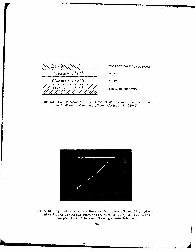
A LOY CONTACT (PARTIAL COVERAGE)
n +GaAs:Sn 10 19 CM-3 ~1M
p ++GaAs: Be 10 20 cm-3 1M
p as n 101 CM- 3 0.05 cm (SUBSTRATE)
Figure 63. Con1figuration oJ n /p- Conducting .1Junction Structure Formed1bY NMBE on Single-crystal GaAs Substrate at 540 0 C
Figure 64. Typical Forward and Reverse Oscilloscope Trace Obtained withn+P- GaAs Conducting Junction Structure Grown by AMBE at -'540 0 C.
on p)+Ga~s.Zn Substrate, Showing Ohmic B3ehavior
92
A second M13E n+/p + + structure was grown at about the same time, andconsisted of thin (~500Ai layers of n+ Sn-doped and )+_ Be-doped GaAs sandwichedbetween lightly doped (1015-1016 cm-3j layers of n-type and p-type GaAs each ~lpmthick. The heavily doped region in this structure was considered to be a closeanalog of the structure believed suitable for forming the connecting intercell ohmiccontacts in the LPE-grown GaAkAs-GaAs cell pair being developed in the Task 5 work(see Section 2. 5). It was found that this structure also exhibited ohmic (i. e., non-rectifying) behavior.
Both of the above structures were subjected to thermal cycling proceduresthat duplicated the temperature-time cycle typical of that involved in LPE growth ofa window-type GaAs solar cell structure. Subsequent examination of the I-Vcharacteristics of both structures indicated no deleterious effect on the ohmic con-duction nature of either structure. The structural parameters and the electricalcharacteristics of these samples both before and after the temperature cycling aresummarized in Table 5.
The I-V characteristics for the first sample after this temperature cyclingare shown in Figure 65 and for the second sample before and after the cycling inFigure 66. The observed behavior of both structures after the heat treatment indi-cated that a satisfactory connecting junction that will survive subsequent processingcan be made by the MBE technique.
Table 5. Structural Parameters and Electrical Properties ofGaAs Nonrectifying Junction Structures Grown by MBE,
before and after Temperature Cycling*
Individual Layer Parameters Measured Contact Resistivity
Before Temp. After Temp.Sample Cond. Carrier onc. Thickness Cycling Cycling
Designation Type (cmi) Dopant (pm) (ohm-cm 2 ) (ohm-cm 2 )
236 n+ 1019 Sn 1.5 0.13 0.196
++ 1020 BP 1.8
p+ 1 101 Zn (substrate)
239 n 1016 Sn 1 0.31 0.123
n + 2x10 19 Sn 0.05
+ 1p 5x10 19 Be 0.05
p 1016 Be I
+ 1019 Zn (substrate)
*Temperature cycling duplicated that associated with LPE growth of window-type solar cell structure inGaAAs-GaAs materials system.
93
I
ih,,_
Figure 65. Forward and Reverse I-V Characteristics of n /p + GaAsConducting Junction Structure of Figure 64 Grown by MBE at -540 0 C
on p'GaAs:Zn Substrate, after Temperature Cycling Duplicatingthat Encountered in LPE Cell Growth
2.2.4.3 Optical Properties of GaAs Tunneling Junctions
To assess the possible optical absorption losses associated with GaAs tunneljunctions, a review of the below-bandgap-energy absorption data for highly dopedGaAs was made.
The data suggest that to maintain an attenuation of less than 1 percent of the0. 7eV photons by the tunnel junction the p+ layer thickness can be no more than-160A for a doping concentration of 1020 cm and the n+ layer thickness no morethan -1300A for 1020 cm - 3 . For 1019 cm - 3 doping concentrations in each regionthese limiting thicknesses increase to -0. 24 ±m for p+ material and -0. 6jLm for n+
material.
The latter parameters are within the range of those practically attainable withany of the fabrication techniques being considered for producing the stacked multi-junction structures in this program.
2.2.5 Experimental GaAs-Ge SMBSC Structures
A likely configuration for the first experimental two-cell GaAs-Ge SMBSC tobe fabricated by CVD techniques is shown schematically in Figure 67. Although theseparate components involved (GaAs cell, GaAs tunneling junction, Ge cell) weremade separately in the Phase 1 program the entire stacked cell assembly had notbeen fabricated by CVD techniques alone prior to the completion of Phase 1.
94
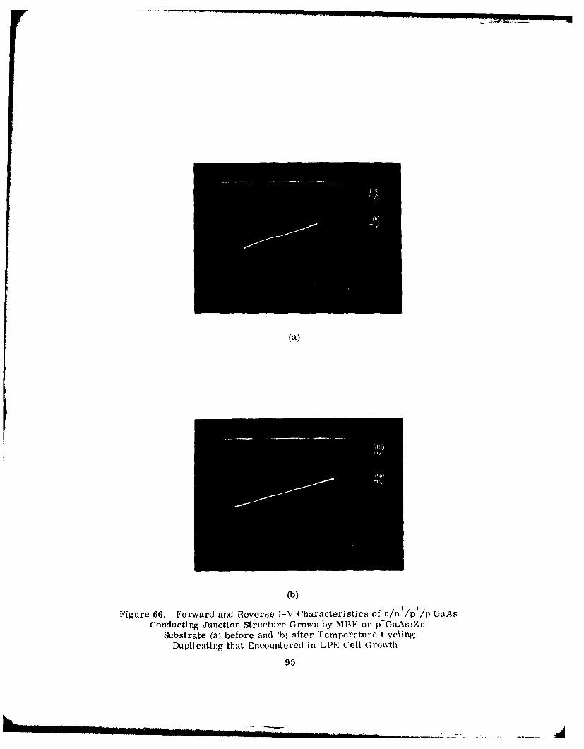
(a)
(b)
Figure 66. Forward and Reverse 1-V Characteristics of n/n+/p /p GaAsConducting Junction Structure Grown by M13E on p GaAs:Zn
Substrate (a) before and (b) after Temperature CyclingDuplicating that Encountered in LPE ('ell Gro%%th
95
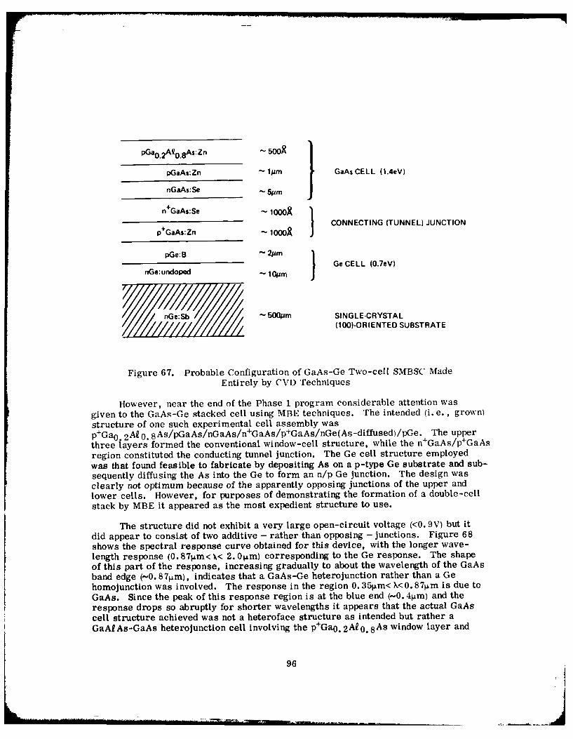
pGa0 .2 AQ0. 8As:Zn - 500R
pGaAs:Zn 1;m1 1 GaAsCELL (1.4eV)
nGaAs:Se 5 Jnn +GaAs:Se - 1000 1
n CONNECTING (TUNNEL) JUNCTIONp+GaAs:Zn ~ 1000 J
pGe:B - 2ymGe CELL (0.7eV)
nGe: undoped - 10pum
n: - 500Am SINGLE-CRYSTAL(100)-ORIENTED SUBSTRATE
Figure 67. Probable Configuration of GaAs-Ge Two-cell SMBSC MadeEntirely by CVD Techniques
However, near the end of the Phase 1 program considerable attention wasgiven to the GaAs-Ge stacked cell using MBE techniques. The intended (i. e., grown)structure of one such experimental cell assembly wasp+Ga 0 2 A20 . 8 As/pGaAs/nGaAs/n +GaAs/ p +GaAs/nGe(A s -diffu s ed) /pGe. The upperthree layers formed the conventional window-cell structure, while the n+GaAs/p+GaAsregion constituted the conducting tunnel junction. The Ge cell structure employedwas that found feasible to fabricate by depositing As on a p-type Ge substrate and sub-sequently diffusing the As into the Ge to form an n/p Ge junction. The design wasclearly not optimum because of the apparently opposing junctions of the upper andlower cells. However, for purposes of demonstrating the formation of a double-cellstack by MBE it appeared as the most expedient structure to use.
The structure did not exhibit a very large open-circuit voltage (<0. 9V) but itdid appear to consist of two additive - rather than opposing - junctions. Figure 68shows the spectral response curve obtained for this device, with the longer wave-length response (0. 87irm< x< 2.0gm) corresponding to the Ge response. The shapeof this part of the response, increasing gradually to about the wavelength of the GaAsband edge (-0.874m), indicates that a GaAs-Ge heterojunction rather than a Gehomojunction was involved. The response in the region 0.351m< X<0.874m is due toGaAs. Since the peak of this response region is at the blue end (-0. 41.m) and theresponse drops so abruptly for shorter wavelengths it appears that the actual GaAscell structure achieved was not a heteroface structure as intended but rather aGaAfAs-GaAs heterojunction cell involving the p+Gao. 2 A 0. 8 As window layer and
96 H
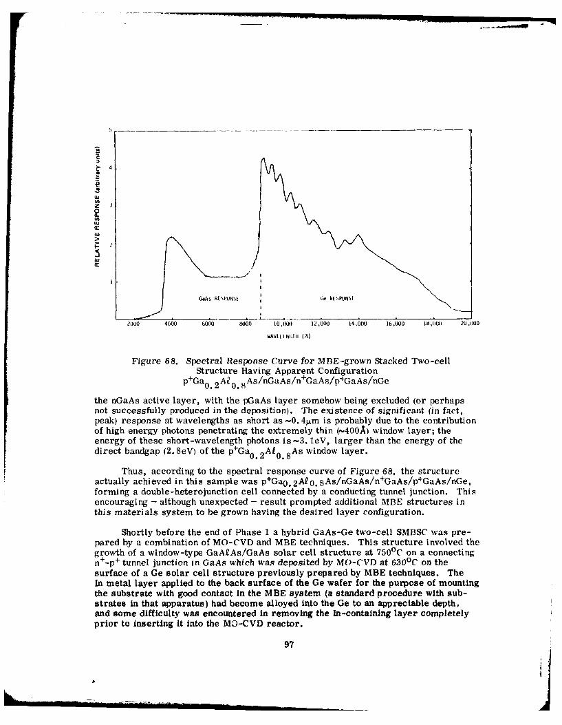
ICz
Uw
Z 30C.
UJ (I,LU
LUL
280 4000 6000 8000 10,000 12,000 14,000 16,00o 180,Mt 2U.000
WAVWI I N 11 (A)
Figure 68. Spectral Response Curve for MBE-grown Stacked Two-cellStructure Having Apparent Configuration
p+Ga0. 2 A2 0.8As/nGaAs/n + GaAs/p +GaAs/nGe
the nGaAs active layer, with the pGaAs layer somehow being excluded (or perhapsnot successfully produced in the deposition). The existence of significant (in fact,peak) response at wavelengths as short as -0. 4 ±m is probably due to the contributionof high energy photons penetrating the extremely thin (-400A) window layer; theenergy of these short-wavelength photons is -3. leV, larger than the energy of thedirect bandgap (2.8eV) of the p+Ga0. 2 Af 0 . 8 As window layer.
Thus, according to the spectral response curve of Figure 68, the structureactually achieved in this sample was p+GaO. 2 AP 0.8As/nGaAs/n+GaAs/p+GaAs/nGe,forming a double-heterojunction cell connected by a conducting tunnel junction. Thisencouraging - although unexpected - result prompted additional MBE structures inthis materials system to be grown having the desired layer configuration.
Shortly before the end of Phase 1 a hybrid GaAs-Ge two-cell SMBSC was pre-pared by a combination of MO-CVD and MBE techniques. This structure involved thegrowth of a window-type GaA2As/GaAs solar cell structure at 7500 C on a connectingn+-p + tunnel junction in GaAs which was deposited by MO-CVD at 630 0 C on thesurface of a Ge solar cell structure previously prepared by MBE techniques. TheIn metal layer applied to the back surface of the Ge wafer for the purpose of mountingthe substrate with good contact in the MBE system (a standard procedure with sub-strates in that apparatus) had become alloyed into the Ge to an appreciable depth,and some difficulty was encountered in removing the In-containing layer completelyprior to inserting it into the MO-CVD reactor.
97
Although the removal was eventually effected, the front surface of the Ge cellstructure %%as slightly damaged, and this adversely influenced the growth of thefive MO-C\I) layers of the tunnel junction and the GaAs window cell. However, thelarge-area structure was completed (the Ge wafer was - 1-1/2 in. in diameter withan SOOA GaO. I Ao..)As p-type window layer on a 1. *tm p-type GaAs:Zn layer on a4. 6 m n-type GaAs:Se base region; the conducting tunel junction consisted ofn'GiAs:Sc/p (aAs:;n, with each layer -0.'3 m thick. Processing of this stackedcell was not completed by the end of Phase 1, however.
Additional SMIBS( structures involving GaAs and Ge solar cells prepared byvarious combinations of MO-('VI) and NIBE techniques are expected to be fabricaledand evaluated in Phase 2, commencing immediately at the start of the program.This combination of cells is of interest not only as a two-cell tandem assembly butalso as the two lower-bandgap cells in a three-cell SMBS(" consisting of GaAk As,GaAs, and Ge cells in series (see Task 4 discussion.
2.3 GaAs-InGaAs SMBSC TECHNOLOGY DEVELOPMENT
This task was to involve the I.PE growth of multiple-bandgap cell structuresin the GaA As-GaAs system and the InP/InGaAs system to produce a two-cellSMBSC. Good overall efficiency was expected for this system, and it was anticipatedthat the series current-conduction problem at the interface between cells would besolvable by interface-defect tunneling. Most experimental cells were expected to begrown on GaAs substrates rather than on prohibitively expensive lnP substrates,although some structures were to be prepared on lnP substrates early in the programfor making various critical comparisons.
As a first step in this task the LPE growth of p lnl' layers on n GaAs single-crystal substrates was to be undertaken. Growth conditions required for control ofthe nPl surface morphology on such substrates were to be determined. Propertiesof the interfaces were to be investigated as functions of various growth parametersAtemperature, doping concentrations, cooling rates) and of the gro\th sequence. Thecurrent conduction mechanism, expected to be dominated by interface-defect tunnelingin this materials system, was to be investigated so that the layer growth conditionsrequired for low-resistance ohmic conduction could be established.
When that was successfully achieved the growth of l.1l- layers of p- and n-typeInGaAs on the p+1nP layers was to be undertaken. The photovoltaic properties of thelnGaAs junction would then be determined, and deposition parameters would then beadusted to optimize the photovoltaic performance for use in the two-cell (GaAs andInGaAs) system.
Next, growkth of p- and n-type lnGaAs LPE layers on )fInl single-crystalsubstrates was to be investigated, and the photovoltaic properties of optimizedlnGaAs junction structures grown on such substrates compared with the photovoltaicproperties of the devices grown on the p+fnP/n'GaAs composites described above.This would indicate if further optimization of the InGaAs cells grown on the com-posites was required for use in the SM13SC assembly.
98
After satisfactory development of the LPE lnGaAs cell structure on thep*InP/n+GaAs substrate, the complete two-cell assembly was to be fabricated bygrowing the GaAf As/GaAs heteroface cell structure by LPE on the second (back)side of the same n4 GaAs single-crystal substrate. The photovoltaic properties ofthe two-cell stack would then be measured and evaluated, and any required modifica-tions in fabrication procedure for the individual component cells would be developed.Finally. the overall growth and fabrication procedure was to be carefully assessed,and any indicated changes to optimize the photovoltaic performance of the completeassembly were to be developed and incorporated.
This task was also expected to involve the evaluation of various contactmaterials and configurations as required, as the work progressed.
2. 3. 1 InP and lnGaAs Layers Grown by LPE
1,14E growth experiments with heavily doped p+ InP layers were begun in thefirst month of the program, using n4 GaAs single-crystal substrates. However, thesurface morphology of the initial lil films on GaAs was unsatisfactory. The effectsof changes in growth temperature, degree of super-cooling of the melt, and coolingrate after growth were investigated in an attempt to improve the quality of the lnPsuraces.
Preliminarv l.11E growth experiments were also begun at about the same timeiin a separate apparatusi on the InGaAsi materials systems. Although this(tuaternary was intended for eventual use as the 1.0 eV cell material for the LPEthree-cel! SMBS(" (Task 51, exploratory experiments with growth of the small-handg~alp i-O. 7eV1 ternary lnGaAs were undertaken first.
Single-crystal suhstrates of pl l of two different orientations were also usedfor the experimental grow.th of nlnl , layers, as a preliminary step to growingn'InGaAs followed by p*lnGaAs lavers. These experiments were limited at the timeto an evaluation of the effects of crvstallographic orientation of the substrate uponthe surface morphology of the Ini) films. ()nce a preferred orientation for the single-crstal Inl' substrate was identified - presumably one of the three orientations (1001,ll lAi, (11111) - additional substrate wafers were to be prepared and some three-
laver experimental structures grown.
The composition of InGaAs selected for use as the 0. 7eV (-ell material was thatwhich is lattice-matched to fnP and has the approximate composition In0 n.,Ga 0 As.The use of an Ini ) window for the small-bandgap cell should not cause seriousabsorption loss of usable solar radiation transmitted by the top cell (GaAs), sincethe bandgap energy of InP is only slightly smaller than that of GaAs. If the windowmaterial used for the small-bandgap cell has a significantly smaller bandgap energy,than that of GaAs then appreciable absorption losses would result, so the choice ofthe window material (and thus the material on which to grow the small-bandgap cellstructure) is quite restricted. Examination of appropriate bandgap-vs-latticeconstant diagrams for various compositions of materials indicated that possiblewin(low materials include lnGa) (Eg > 1.4cV), InGaAsl' (Eg > 1.4eV), AfInAs, andGaAInAs, in addition to ln itself.
99
The lnP LPE growth experiments on GaAs continued with both In and Sn usedas the solvent. Both the growth temperature and the cooling rate were varied, withthe super-cooling of the melt maintained at 5 deg C. The results showed that InPlayers with rather rough surfaces could be grown on (100)-oriented GaAs substratesusing a Sn solution. The In solution, however, attacked the GaAs substrateseverely, and melt was always left on the substrate at the conclusion of the growthexperiment as a result of the rough growth surface.
Growth experiments were then begun with both In and Sn solutions and (li1B)-oriented GaAs substrates, since it had been recently reported that acceptable LPEgrowth of InP on this GaAs plane can be achieved, and good quality epitaxial growthof InP was obtained on this plane previously by MO-CVD at Rockwell ERC. The sub-strates were "cooled" during the deposition process to maintain their temperaturesbelow the normal temperature induced by the process. This procedure appeared tooffer some promise. It was shown that LPE growth at 8000 C resulted in much lessIn inclusion at the InP-GaAs growth interface than was obtained at 600 0 C, but thegrown layer had a smoother surface for the 600 0 C growth than for 800 0 C growth.Subsequent experiments showed that the growth temperature was very critical forgrowth from In solution, with the optimum temperature appearing to be about 5200C,with departures from this by as little as 30 deg C (above or below) causing severeproblems with melt wipe-off.
Several InGaAs p-n junction structures were also grown by LPE on (111B)-oriented single-crystal n41nP substrates. The grown layers were generally smoothbut exhibited small pits in areas away from the crystallographically on-orientationplateaus. The density of these pits was rather low, however, so it was believedthat the photoresponse of the junction devices might not be seriously affected.
Several of the InGaAs p-n junction structures prepared in these experimentswere evaluated by preparing small-area (-0. 025 cmZ) mesa devices. Contact to thep-type InGaAs layer was made by vacuum-deposited Ag-Zn pads, and the n~lnP sub-strate was contacted by means of vacuum-deposited Au-Ge on Pt. The Ag-Zn contacton the p layer did not result in low contact resistance, however, and it furtherexhibited a tendency to ball-up and not wet the InGaAs layer surface during the post-deposition heating cycle.
Figure 69 shows the measured relative spectral response for one of thesedevices when the monochromatic light was incident on the lnP substrate side. Anabsolute quantum efficiency of -20 percent was measured with a 1. 06.rm laser and acalibrated reference diode. This low value indicates that the minority-carrierdiffusion length in the grown InGaAs layer was probably quite low. The typical layerthickness for these growths was also on the low side (< 2 .im), resulting in fast drop-offof the photoresponse at the long-wavelength end. Also, since Zn was used as theacceptor impurity in these structures, Zn contamination of the n-type melt was prob-ably taking place, and some Zn diffusion out of the p-type layer probably alsooccurred during cooling after the growth process was complete, giving rise to thequestion of whether the deposited n-type InGaAs layer actually survived the completegrowth process or not.
100
6
5 5
UUi
cc
0.9 1.0 1.1 1.2 1.3 1.4 1.5 1.6 1.7 1.8WAVELENGTH (p m)
Figure 69. Spectral Photoresponse of LPE InGaAs p-n Junction Cellwith Illumination Incident through InP Substrate
The dark I-V characteristics of these devices showed high values for n (closeto 3), indicating that the current transport was not the ideal type (injection over thep-n junction barrier). Although the temperature dependence of the I-V characteristicswas not measured, it was expected that current transport in these devices was of thedefect-assisted tunneling type that has been observed in many heterojunction devicestructures; that is, it appeared that a heterojunction between InP and InGaAs hadresulted, rather than a simple p-n junction in InGaAs.
Figure 70 shows the measured dark and illuminated I-V characteristics of oneof the mesa devices as measured using a curve tracer and a microscope lamp forillumination. The open-circuit voltage of >0. 3V and short-circuit current of-2mAare close to the expected values; however, the poor fill-factor was due to the excessforward current caused by the defect-assisted tunneling mentioned above.
To correct this situation new structures were grown with the goal of obtainingthicker InGaAs layers adjoining the substrates. One such experiment produced ann-type layer 1. 5pm thick and a p-type layer 1. 9 km thick. However, preliminarymeasurement of the photovoltaic properties indicated very weak photoresponse, forreasons not known. The possibility that poor ohmic contacts were involved and thusrendered the photovoltaic response measurements invalid led to the fabrication ofcomplete devices with proper contacts for further evaluation. These also exhibitedunsatisfactory photovoltaic properties, however.
101
aA
Figure 70. Dark and Illuminated I-V Characteristics of InGaAs p-nJunction Measured with Microscope Lamp Illumination
(Voc > 0.3V, Ise = 2mA)
In an attempt to circumvent some of the LPE growth problems encountered inthis materials system, experiments were planned in which InP n-type layers thathad been previously grown on single-crystal GaAs substrates by the MO-CVDprocess would be used as growth surfaces for the LPE growth of InGaAs. Samplesin which the MO-CVD InP layers were 2-6 pyn thick were obtained, to attempt toreduce the effects of InP decomposition and avoid complete dissolution of the n-typelayer during the initial etch-back stage in the LPE growth process. Subsequently, aspecial group of InP layers was prepared by the MO-CVD process with thicknessesranging from 7.5 to 10 urn, to further alleviate this problem.
First, however, in preparation for LPE growth experiments with these sub-strates, several lnP deposition experiments were done with bulk InP substrates atvery low temperatures - below 5000C - using In solutions. These preliminary runswere considered necessary to minimize the possibility of losing the first group ofrelatively thin MO-CVD InP layers during the etch-back step. Unfortunately, goodquality InP growth was not achieved In these experiments with bulk substrates.
Since early in the program, a number of experiments had been carried out withthe LPE growth of InP on GaAs substrates. The experiments had involved growthfrom both In and Sn solutions, growth on (100) and (111) A end B surfaces, growthtemperatures from 600 to 800 0 C, and the use of large vertical temperature gradientsacross the liquid-solid interface to minimize etch-back and enhance growth in a
102
rnonequilibrium situation. While some of the InP layers appeared adequate forsubsequent InGaAs epitaxial growth, examination of the structures under an infraredtransmission microscope revealed large numbers of In inclusions completely opaqueto near-IR radiation. Thus, while such nP layers might prove to be an adequatesubstrate for subsequent InGaAs growth, the interface problem would prevent theiruse in a stacked multiple-bandgap solar cell configuration. That is the situation thatdirected attention to the growth of InGaAs on nP and on a GaAs substrate whichpreviously had an MO-CVD InP layer grown over its surface.
Since most of the initially available MO-CVD lnP layers were relatively thin(<_ 5±m) it was necessary to grow at very low temperatures to avoid InP decomposi-tion prior to epitaxial growth. Growth of InP at 450 0 C proved very difficult becauseof the low 1P solubility in In at that temperature. However, InGaAs growth at that lowtemperature was expected to be easier because of the higher As solubility in InP.
LPE growth of an In0 . 4 7Ga 0 . 5 3 As layer was undertaken on one of the thickerInP/GaAs composite samples previously prepared by MO-CVD. The undoped n-typeInP layer had been deposited at -725oC on a (111B)-oriented GaAs substrate, with aresulting InP thickness of -7. 5Lm. The resulting InGaAs layer grown by LPE wasfound to be spotty and discontinuous, with very poor melt wipeoff. This result wasbelieved to be due simply to the extreme caution that was exercised to preventexcessive meltback of the CVD InP layer and the possible consequent melt attack ofthe underlaying GaAs substrate. The absence of meltback apparently permittedretention of oxides and other impurities at the growth interface, thus interfering withthe epitaxial growth process.
The next experiments were done with bulk crystal InP substrates rather thanthe CVD layers until the LPE growth parameters were more satisfactorily defined.Successful growth of an InGaAs layer by LPE was achieved with (111B)-orientedp+InP single-crystal substrates that were lapped to an acceptable thickness and thenpolished prior to the deposition experiments.
Growth was accomplished by contacting the substrate to the melt at a tempera-ture -0. 5 deg C above the measured saturation temperature. This procedure provided0. 5-1. 0Lm of substrate etch-batch and appeared to be a crucial factor in obtainingsuccessful growth in this materials system. The grown layer was not intentionallydoped, but subsequent electrical characterization indicated the layer to be n type.Growth was initiated at about 6290 C and proceeded with a cooling rate of -1 deg Cper min. Under those conditions the average growth rate for the InGaAs was slightlyabove 1Lm/deg C. The actual composition of the layer was not determined, but thegeneral quality of the growth suggested there was close lattice match between thelayer and the InP, implying a composition very close to Ino. 47Ga0 . 53As. The band-gap for such a composition would be 0. 7eV - nearly identical to that of GaSb.
Although the InGaAs layer appeared mirror-like to the unaided eye, at highmagnifications numerous lens-shaped surface features were visible. It was specu-lated that these may have resulted from the cooling rate being too rapid. Similarbut more pronounced surface features have been reported by Sankaran et al (Ref 10)
103
and were attributed to local Ga concentration gradients and fluctuations at the growinginterface caused by the large Ga distribution coefficient (KGa Z 6. 12) in this type ofmelt.
It was expected that a p-n junction had been formed in the grown n-type InGaAslayer due to the known rapid out-diffusion of Zn from the p+InP substrate. One of thestructures was processed into individual mesa-type solar cells (0. 025 cm x 0. 025 cm)for photovoltaic evaluation. The substrate was thinned to about 4 mils by a combina-tion of lapping and etching to reduce the free-carrier absorption losses of photonsentering the cell structure from the InP side prior to their reaching the p-n junctionregion in the InGaAs.
A full-coverage Au-Ge contact layer -2000A thick was applied to the n-typesurface of the InGaAs layer and sintered at 4500 C in H2 for 1 min. Because of theproblem that sometimes occurs in contacting p+InP, several small pieces were takenfrom the as-grown composite structure for use in contact optimization experiments.With a pattern of 10-mil diameter dots used as a test grid it was found that satis-factory ohmic behavior was provided by contacts of Au(500o)/Zn(500A)/Au(1500A)vacuum-deposited sequentially on the lnP followed by sintering at 4500 C in H2 for1 min. After preparation of the contacts by these techniques on the main part of thecomposite wafer it was then cleaved into individual 0. 025 cm x 0. 025 cm solar cellsfor testing.
Thess devices consistently exhibited short-circuit current densities of-16mA/cm and open-circuit voltages of < 0. IV under AM1 illumination (simulated).The very low Voc values were believed to be caused by large dark saturation currentdensities and poor (i.e., high) diode factors. This view was supported by the strongobserved sensitivity of Voc to the incident light intensity. Using a focused micro-scope lamp as light source and varying the intensity of illumination on the cell it waspossible to obtain data showing the variation of Voc with Jsc over a reasonable range.The relation
V ~n ' K 2n (SC + )Voc q
was then used to determine that n=1. 9 and Jo =4. 75 x 10 A/cm for these devices.These values can be compared with those obtained for GaSb cell structures (see nextsection), for which n=1.7 and Jo =4 x 10- 4 A/cm 2 .
Representative dark and illuminated I-V curves obtained with one of thesecells using the microscope lamp are shown in Figure 71. The strong dependence ofVoc on incident light intensity is evident in the figure. The cause of the large Joobserved in the InGaAs devices was not identified. Some indication was found thatthe structure may have contained a weak blocking diode in addition to the main activep-n junction. However, more work is needed to establish if such a second diode (ifpresent) is caused by a valence-band energy spike at the InP-InGaAs interface -perhaps formed during the LPE growth process - or is simply the result of sub-sequent steps in the cell fabrication process (see below).
104h6i
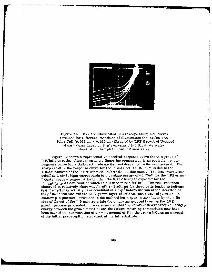
Figure 71. Dark and Illuminated (microscope lamp) I-V CurvesObtained for Different Intensities of Illumination for InP/InGaAs
Solar Cell (0. 025 cm x 0. 025 cm) Obtained by LPE Growth of Undopedn-type InGaAs Layer on Single-crystal plInP Substrate Wafer
(Illumination through thinned InP substrate)
Figure 72 shows a representative spectral response curve for this group ofInP/InGaAs ceils. Also shown in the figure for comparison is an equivalent photo-response curve for a GaSh cell made earlier and described in the next section. Thesharp cutoff in the response curve for the InGaAs cell at- 0. 95 Lm is due to the1.35eV bandgap of the InP window (the substrate, in this case). The long-wavelengthcutoff at 1.65-1. 701tm corresponds to a bandgap energy of-0. 75eV for the LPE-grownInGaAs layers - somewhat larger than the 0. 7eV bandgap expected for theIn 0 5 3 Ga 0 4 7 As composition which is a lattice match for InP. The peak responseobserved At relatively short wavelength (-1.05 p m) for these cells tended to indicatethat the cell may actually have consisted of a p-p+ heterojunction at the interface ofthe p+InP substrate and the LPE-grown layer of InGaAs, and a second junction - ashallow p-n junction - produced in the undoped but n-type InGaAs layer by the diffu-sion of Zn out of the InP substrate into the otherwise undoped layer as the LPEgrowth process proceeded. It was suspected that the apparent discrepancy in bandgapenergy between the grown material and the lattice-matching composition may havebeen caused by incorporation of a small amount of P in the grown InGaAs as a resultof the initial predeposition etch-back of the InP substrate.
105
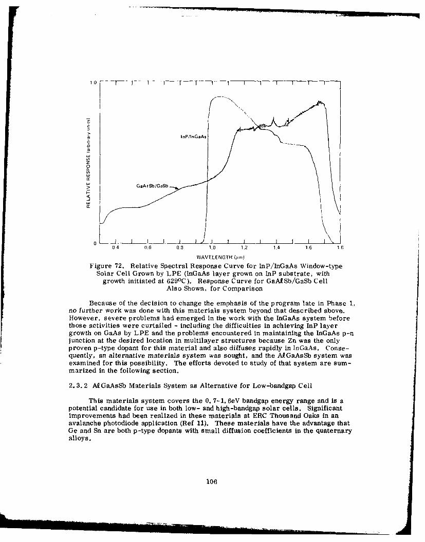
o10 - ~1 J - -TI I I I
1 0
C
InP/InGaAs
0
w
0Wuo
>"GaAfSb/GaSb
0.4 0.6 0.8 1.0 1.2 1.4 1 6 1 B
WAVELENGTH (Imri
Figure 72. Relative Spectral Response Curve for lnP/InGaAs Window-typeSolar Cell Grown by LPE (InGaAs layer grown on InP substrate, with
growth initiated at 629 0 C). Response Curve for GaAISb/GaSb CellAlso Shown, for Comparison
Because of the decision to change the emphasis of the program late in Phase 1,no further work was done with this materials system beyond that described above.However, severe problems had emerged in the work with the InGaAs system beforethose activities were curtailed - including the difficulties in achieving InP layergrowth on GaAs by LPE and the problems encountered in maintaining the InGaAs p-njunction at the desired location in multilayer structures because Zn was the onlyproven p-type dopant for this material and also diffuses rapidly in InGaAs. Conse-quently, an alternative materials system was sought, and the AlGaAsSb system wasexamined for this possibility. The efforts devoted to study of that system are sum-marized in the following section.
2. 3. 2 M GaAsSb Materials System as Alternative for Low-bandgap Cell
This materials system covers the 0. 7-1. 6eV bandgap energy range and is apotential candidate for use in both low- and high-bandgap solar cells. Significantimprovements had been realized in these materials at ERC Thousand Oaks in anavalanche photodiode application (Ref 11). These materials have the advantage thatGe and Sn are both p-type dopants with small diffusion coefficients in the quaternaryalloys.
106kL
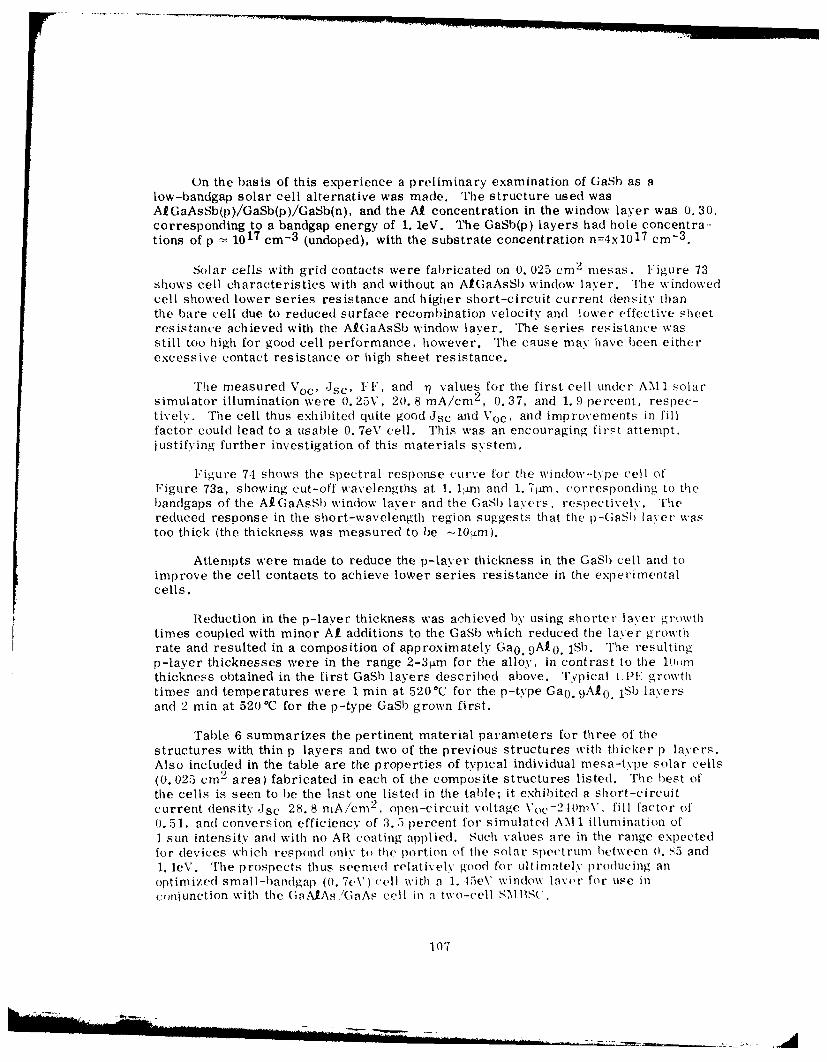
On the basis of this experience a preliminary examination of GaSb as alow-bandgap solar cell alternative was made. 'ihe structure used wasAIGaAsSb(p)/GaSb(p)/GaSb(n), and the At concentration in the window layer was 0. 30,corresponding to a bandgap energy of 1. 1eV. The GaSb(p) layers had hole concentra-tions of p o 101 7 cm- 3 (undoped), with the substrate concentration n=4x10 1 7 cm - 3 .
Solar cells with grid contacts were fabricated on 0.025 cm 2 mesas. Figure 73shows cell characteristics with and without an AIGaAsSb window layer. The windowedcell showed lower series resistance and higher short-circuit current density thanthe bare cell due to reduced surface recombination velocity and lower effective sheetresistance achieved with the AIGaAsSb window layer. The series resistance wasstill too high for good cell performance, however. The cause may have been eitherexcessive contact resistance or high sheet resistance.
The measured Voc, Jsc, FE, and pj values for the first cell under AMI solarsimulator illumination were 0. 25V, 20. 8 mA/cm 2, 0.37, and 1. 9 percent, respec-tively. The cell thus exhibited quite good Jsc and Voc, and improvements in fillfactor could lead to a usable 0. 7eV cell. This was an encouraging first attempt,justifying further investigation of this materials system.
Figure 74 shows the spectral response curve for the window-type cell ofFigure 73a, showing cut-off wavelengths at 1. 1 .mi and 1. 7im, corresponding to thebandgaps of the AIGaAsSh window layer and the GaSh layers, respectively. Thereduced response in the short-wavelength region suggests that tile p-GaSh layer wastoo thick (the thickness was measured to be -10pgm).
Attempts were made to reduce the p-layer thickness in the GaSh cell and toimprove the cell contacts to achieve lower series resistance in the experimentalcells.
Reduction in the p-layer thickness was achieved by using shorter layer growthtimes coupled with minor At additions to the GaSh which reduced the layer growthrate and resulted in a composition of approximately Ga 0 . 9 A1 0 . 1Sb. The resultingp-layer thicknesses were in the range 2-3iim for the alloy, in contrast to the 10amithickness obtained in the first GaSh layers described above. Typical .PI.- growthtimes and temperatures were 1 min at 520'C for the p-type Ga 0 . 9 AI0. 1Sb layersand 2 min at 520°C for the p-type GaSh grown first.
Table 6 summarizes the pertinent material parameters for three of tilestructures with thin p layers and two of the previous structures with thicker p layers.Also included in the table are the properties of typical individual mesa-type solar cells(0. 025 cm 2 area) fabricated in each of the composite structures listed. The best ofthe cells is seen to be the last one listed in the table; it exhibited a short-circuitcurrent density Jsc-28. 8 mA/cm 2 , open-circuit voltage Voc-2.omV, fill factor of0. 51, and conversion efficiency of 3. 5 percent for simulated AM 1 illumination ofI sun intensity and with no Al coating applied. Such values are in the range expectedfor devices which respond onl to the portion of the solar spectrum Ibetween 0. S5 and1. 1eV. The prospects thus seemed relatively good for ultimately producing anoptimized small-handgap (0. 7eV) cell with a 1. 15eV window layer for use inconjunction with the GaAIAs (;nAs cell in a two-cell SMBiSC.
107
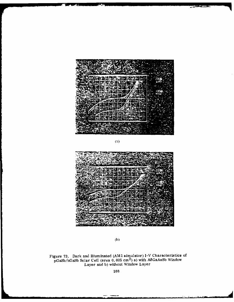
MW low-,J
Layerand b) withotWno ae
108
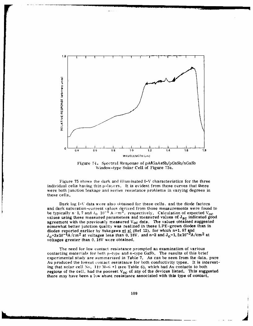
1.0 I I I I I I ! I I I I 1
C
1.0
0
0.4 06 08 10 1.2 1.4 1.6 1.8
WAVFLENGTif (pnii
Figure 74. Spectral Response of pA1GaAsSb/pGaSb/nGaSbWindow-type Solar Cell of Figure 73a.
Figure 75 shows the (lark and illuminated I-V characteristics for the threeindividual cells having thin p-laye(rs. It is evident from these curves that therewere both junction leakage and series resistance problems in varying degrees inthese cells.
Dark log I-V data were also obtained for these cells, and the diode factorsand dark saturation-current values derived from those measurements were found tobe typically n- 1. 7 and JO 10 - 4 A / m 2 , respectively. Calculation of expected Vocvalues using these measured parameters and measured values of Jsc indicated goodagreement with the previously measured Voc data. The values obtained suggestedsomewhat better junction quality was realized in these LPE-grown diodes than indiodes reported earlier by Sukegawa et al (Ref 12), for which n=1. 87 andJo=3xl0-4A/cm 2 at voltages less than 0 18V, and n=2 and Jo=1. 5xl0- 3 A/cm2 at
voltages greater than 0. 18V were obtained.
The need for low contact resistance prompted an examination of variouscontacting materials for both p-type and n-type GaSb. The results of this briefexperimental study are summarized in Table 7. As can be seen from the data, pureAu produced the lowest contact resistance for both conductivity types. It is interest-ing that solar cell No. 119 M-(; #1 (see Table 6), which had Au contacts to both
regions of the cell, had the poorest Voc of any of the devices listed. This suggestedthere may have been a low shunt resistance associated with this type of contact.
109
U r -1 M C.n
LA. N c'1(i o
2LE c co to G
^4 -9 % - N~ r4
W Mas o D U
4 ~ ~ 4 = ~ l c .
0 -4- 4 4
0 00
0 cl0
4c~~. 0. 4 . c.P~ ?
D'L (G-~
0 .ci~ -M4s 4n 4 -
Cd~ __ _
cd 0
N- N - -
O) L) 4 C.
4C CL c (1
-4 C, -E -~C o .
-d 4 f
csI- s .< c2 .0 .E*d Q) 3 ((a
=o in ca X-
a aC E~
c± - , *a 4- *=a ca- C; C; L
110
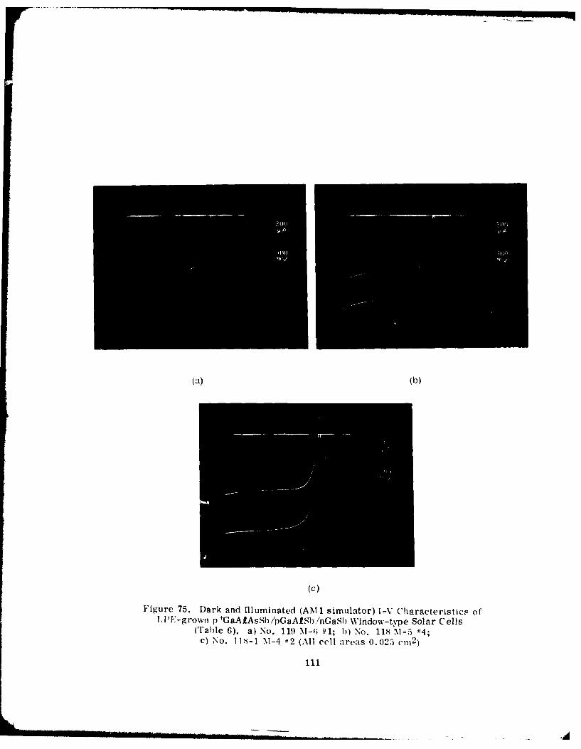
(a) (1))
(C)
Figure 75. Dark and Iliuminated (AMl1 simulator) I-V Characteristics ofLPE-grown p+GaAIAsS/pGaASb/nGaS) Window-t-pe Solar Cells
(Table 6). a) No. 119 M-6 ft1; b) No. 118 M-5 14;c No. I l -1 M-4 t2 (All cell areas 0.025 cm 2 )
111
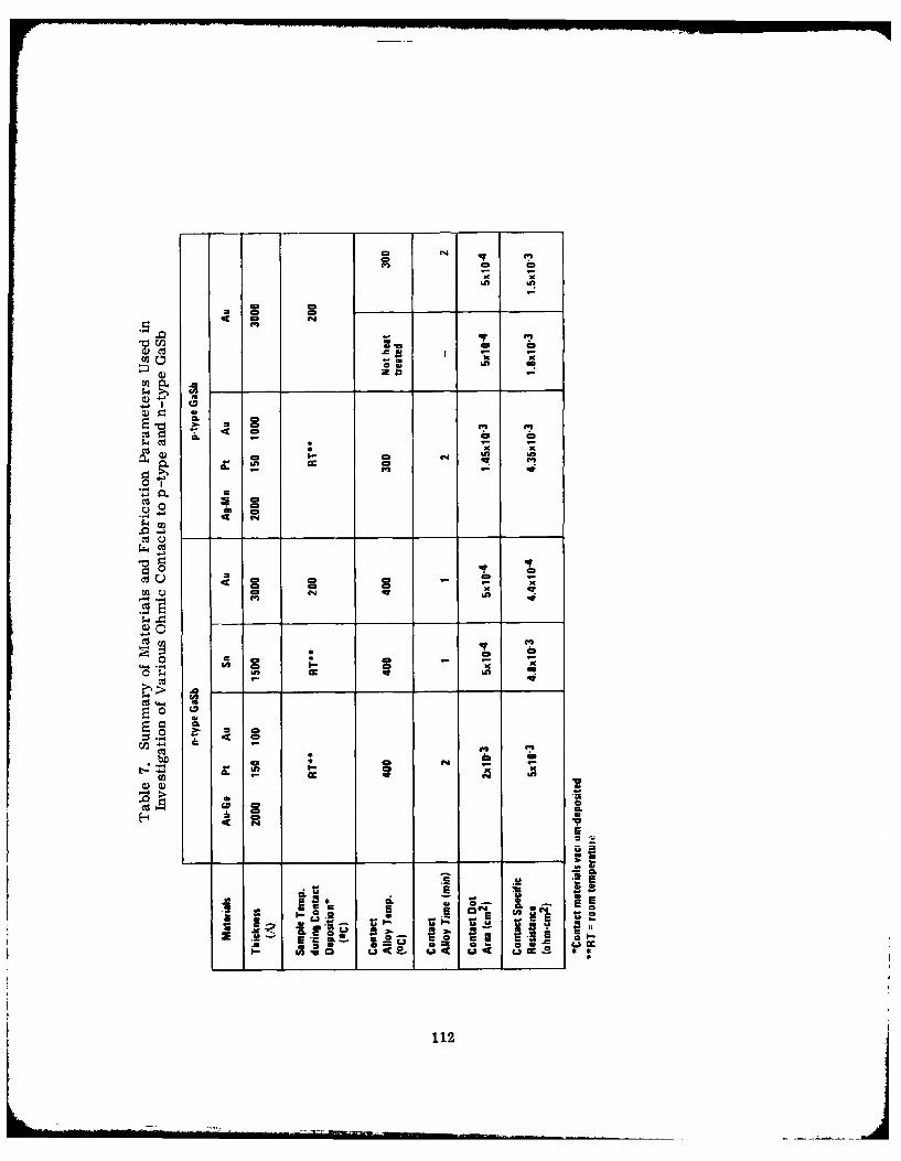
x 1;
2 a ,
ca a
42.
FS a 6a
CL. eli
0.
*' xMr a V4 Nr6
asa
0 C, - x
U - a C0~ ~ ;- N c n
m - .
4.1 > .
- 4.,
CU -
4 aO
cc
112
Additional attempts were made to grow window-type cell structures with higherAt composition (-0. 7) in the window layer, but a series of apparatus problemsoccurred that seriously delayed progress for a time. Those difficulties wereresolved and additional GaAISb/GaSb cell structures were again successfully grownand processed into solar cells late in Phase 1, at about the time the shift inprogram emphasis was adopted.
As a result, no further work was done with this materials system in the Phase 1program.
2.4 GaAI'As - GaAs - Gi-AsSb SMBSC TECHNOLOGY DEVELOPMENT
This task was initially planned to involve growth of the three individual cellcomponents by the MO-CVD process, with subsequent integration of the three intoa single SMBSC assembly. It was anticipated that single-crystal GaAs would beused as the substrate for the composite structure and that each of the three cellswould be grown with an appropriate window material. Because of the complexityof the three-cell SMBSC and the fact that little was known about 2. 0eV GaAIAs cellsor 1. 0eV GaAsSb cells, individual materials properties as well as the properties ofeach of the cell structures were to be extensively characterized as this taskprogressed.
The conduction properties of n+-p + junctions prepared in GaAfAs compositelayer structures were to be studied for various MO-CVD growth conditions.Deposition parameters resulting in high interface doping concentrations and abrupttransitions in doping impurity were to be determined, so that the required low-resistance nonrectifying junctions could be achieved in Ga.AIAs.
Single-crystal n+GaAs substrates were then to be used for the MO-CVD growthof GaAIAs layers successively doped n and p type to produce a 2. 0eV p-n junctionsolar cell in the alloy. This was expected to require considerable experimentationwith both layers; although the GaAfAs alloy system was already extensivelydeveloped by both MO-CVD and LPE and has an available lattice-matched window,the 2. 0eV composition is close to the direct-indirect gap crossover compositionand the minority carrier properties are not well known in this composition region.However, GaAIAs can be grown with compositions throughout the entire range byMO-CVD, so the required layers were to be prepared and their pertinent materialsproperties--including minority carrier diffusion length and surface recombinationcharacteristics--determined to assist in evaluation of this alloy system forthe 2. 0eV cell material. The characteristics of the p-n junction cells resultingfrom these investigations were also to be determined, to complete the evaluation.
Upon successful development of a satisfactory GaAIAs 2. 0eV cell, thatstructure was to be combined with the well-developed GaAlAs/GaAs solar cellstructure on a single n+GaAs substrate, utilizing the nonrectifying n+-p+ tunnelingjunction in GaAfAs mentioned above and planned for development earlier in theprogram. The MO-CVD growth sequence was expected to involve first the depositionof the conventional GaAIAs/GaAs cell (with a p+ upper layer) on the n+GaAs substrate,
113
followed next by deposition of the n+/p + connecting junction, and then by depositionof tie 2. 0eV p/n GaAIAs cell. Deposition parameters were to be optimized toachieve the best photovoltaic performance for this two-cell SMBSC assembly,which would then be used in the complete three-cell structure to fabricated later.
The 1. 0eV cell material originally planned for development for use in thisthree-cell SMBSC was the GaAsSb alloy system, already discussed in Section 2.3.2.GaAs single-crystal substrates were to be used for growth of p- and n-type GaAsSblayers by the MO-CVD technique. The required 1. 0eV bandgap corresponds to thecomposition of GaAsxSbl-x for which x - 0.5, with a lattice constant of about 5. 82A.Although this alloy composition had not been grown by MO-CVD, little difficulty wasanticipated in achieving such material. When satisfactorily doped layers of bothtypes were obtained the two were to be combined to produce p-n junction cells of thedesired bandgap and the deposition parameters adjusted to provide satisfactoryphotovoltaic performance. Lattice-matched GaAIAsSb window layers would then beprepared (also by MO-CVD) for this 1. 0eV cell structure and the overall photovoltaicproperties determined.
It was anticipated that once the MO-CVD GaAsSb 1. 0eV cell was satisfactorilydeveloped it would then be possible to combine all of the structures into a single three-cell SMBSC. To accomplish this the 1. 0eV cell would be grown by MO-CVD on thesecond (back) side of the n+GaAs substrate that was also used for the growth of thetwo-cell (GaAfAs and GaAs) SMBSC configuration on its front surface. Attentionwas to be given to achieving the required nonrectifying conducting interface betweenthe n+GaAs substrate and the heavily doped p+GaA1AsSb window layer of the 1. 0eVcell. The deposition sequence, layer thicknesses, specific layer compositions anddoping concentrations, MO-CVD growth parameters used in preparing the three-cellcomposite, and matarials and processes used for producing low-resistance ohmiccontacts were then to be examined, and the overall fabrication process modified asneeded to produce the desired photovoltaic performance in completed three-cellSMBSC structures. (Some of these areas were investigated as part of the LPE workdone with this materials system in Task 3, described in Section 2.3.2.)
Partly because the properties of 2. 0eV GaAlAs and 1. 0eV GaAsSb were notwell known at that time and partly because InGaP and InGaAsP had both been grownas thin films and fulfill the bandgap requirements for the 2. 0eV and 1. 0eV cellmaterials, respectively, these two materials prepared by MO-CVD were consideredalternates for possible use in the three-cell SMBSC assembly. Such parallel studies,if undertaken, would occur at a much lower level of effort than the primary activity.Solar cell junction structures of each material would be grown on single-crystalGaAs substrates by MO-CVD techniques, and the measured photovoltaic propertiesof such devices would be compared with those of the GaAAs and the GaAsSb cells.If continuing serious difficulties were encountered in achieving the required perform-ance for the GaAlAs cell and/or the GaAsSb cell then either or both of the In systemmaterials would be further developed as substitutes.
This initial overall plan for this task was modified late in the Phase 1 program,when the change in program emphasis was adopted. For the balance of Phase 1 thework of the task was restricted to the GaAIAs-GaAs two cell SMBSC configurationand to the possibility of a GaAIAs-GaAs-Ge three-cell SMBSC assembly.
The activities of this task in the Phase 1 program are summarized in the
following sections.
114
2.4. 1 GaAfAs Solar Cells
Growth of the 2. 0eV GaAIAs cells needed for the three-cell SMIBS( to bedeveloped Using MO-CVI) techniques required accurate calibration and control ofthe composition of the GaAfAs layers. Installation of a new source tank oftrimethylgallium (TMG) on the reactor system used initially for this work madeit necessary for several deposition experiments devoted to checking both the back-ground impurity level in pure GaAs films grown with the new source and thedependence of the alloy composition (i.e., the value of x in Gal-xAixAs) upon the
relative flow rates of the TMG and trimethylaluminum (TMAI) reactants.
Alloy films with 0. 12£x£0. 80 were grown and characterized for compositionby x-ray double-crystal diffractometer measurements and - for those films with
composition in the direct-bandgap region - by room-temperature photoluminescencemeasurements of the energy gap. The results of the two measurements were found
to correlate very well and the compositions thus determined indicated that the
calibration of reactant concentration (i. e., flow rate) versus expected IaYer com-
position was quite accurate for this alloy system.
A malfunction of the MO-CVD epitaxial reactor used for growth of GaAs andGaAlAs structures occurred early in the program. The mass flow controller thatcontrolled the TMAI flow rate into the deposition chamber began functioningincorrectly and so was replaced; several performance checkout runs were made toreestablish the parameters required for obtaining the appropriate alloy composition.
Additional Ga1_xAixAs p-n junction structures were then grown, primarilywith x = 0.37 and at-7500 C. These were found to exhibit good I-V characteristics.Figure 76 shows the dark and illuminated (microscope lamp) I-V curves for a mesadiode (50 mil x 50 mil) fabricated in a junction structure in Ga 0 . (;:3A1 0 . 3 7 As. Therelatively small photoresponse shown is due in large part to the fact that the devicedid not have a window layer of Gal-xAfxAs (with x>0. 8) to reduce the effects of thehigh surface recombination velocity. However, the diode I-V curve shape is quite
good.
Subsequently, along with the preparation of experimental tunneling junctionstructures in Gal-xAfxAs at lower deposition temperatures (see Section 2.4.2),p-n junction devices were also grown in Gal-xAtxAs at-7000 C rather than at- 750 0 C.These structures involved p-type and n-type Ga 0 . 6A1 0 4 As (Eg = 1. 92eV) grown byMO-CVD on GaAs:Si substrates. A thin p+ GaAs:Zn cap layer was grown on topof the GaAIAs p-n junction structure to permit good ohmic contact to be made. Thewafers were processed into 50 mil x 50 mil mesa diodes with 25 mil x 25 mil con-tact pads, and the I-V curves were examined with the curve tracer and mechanicalprobe contact. Good I-V characteristics were obtained, as indicated by therepresentative curve shown in Figure 77.
115
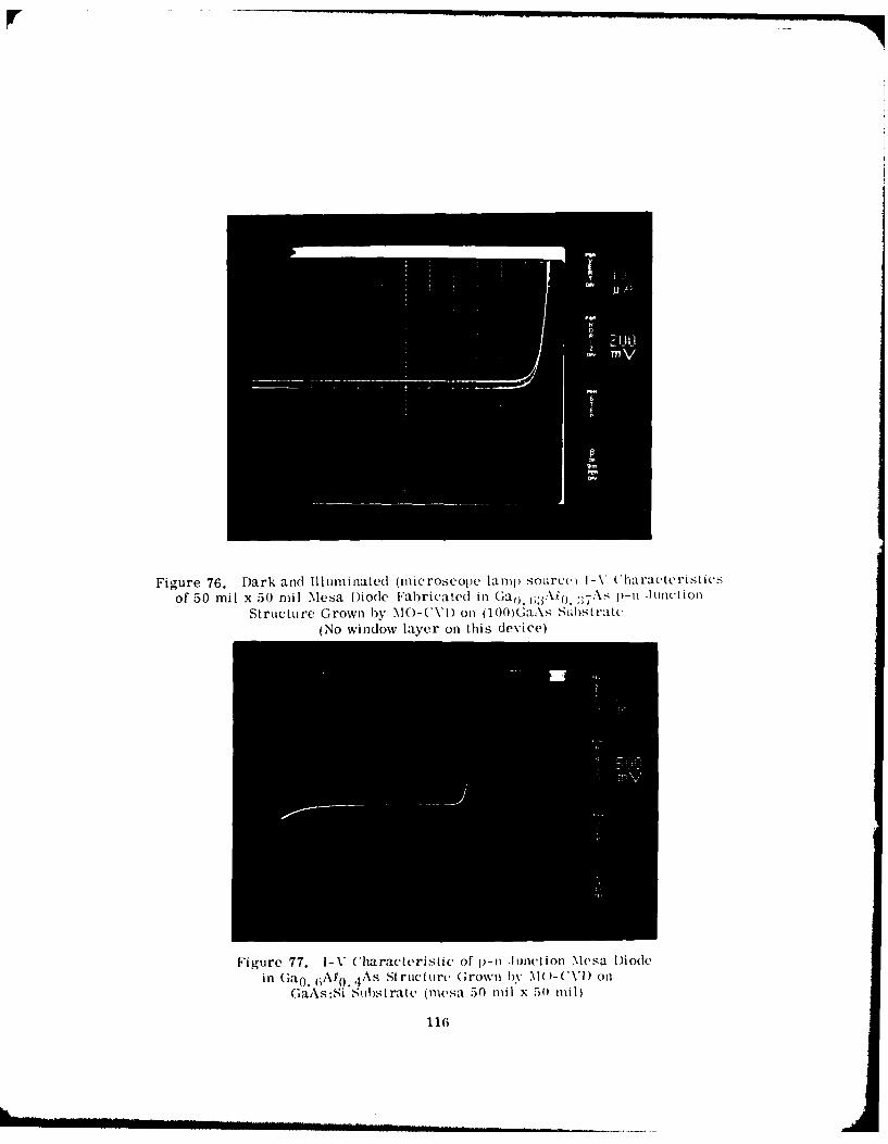
Figure 76. Dark and Illuminated (microscope lamp source, I-V Characteristics
of 50 mil x 50 mil Mesa Diode Fabricated in Gao. ;.V0). : 7 .:\s I)-1 .Jtlnt'tiOl
Structure Grown by MO-C'VI) on (100)GaAs Substrate(No window layer on this device)
Figure 77. I-V Characteristic of p-n Junction .Mesa Diodein Gao. (;Alo.,As Structure Grown by M()-V('I) on
GaAs:Si Substrate (mesa 50 mil x 50 mil)
116;
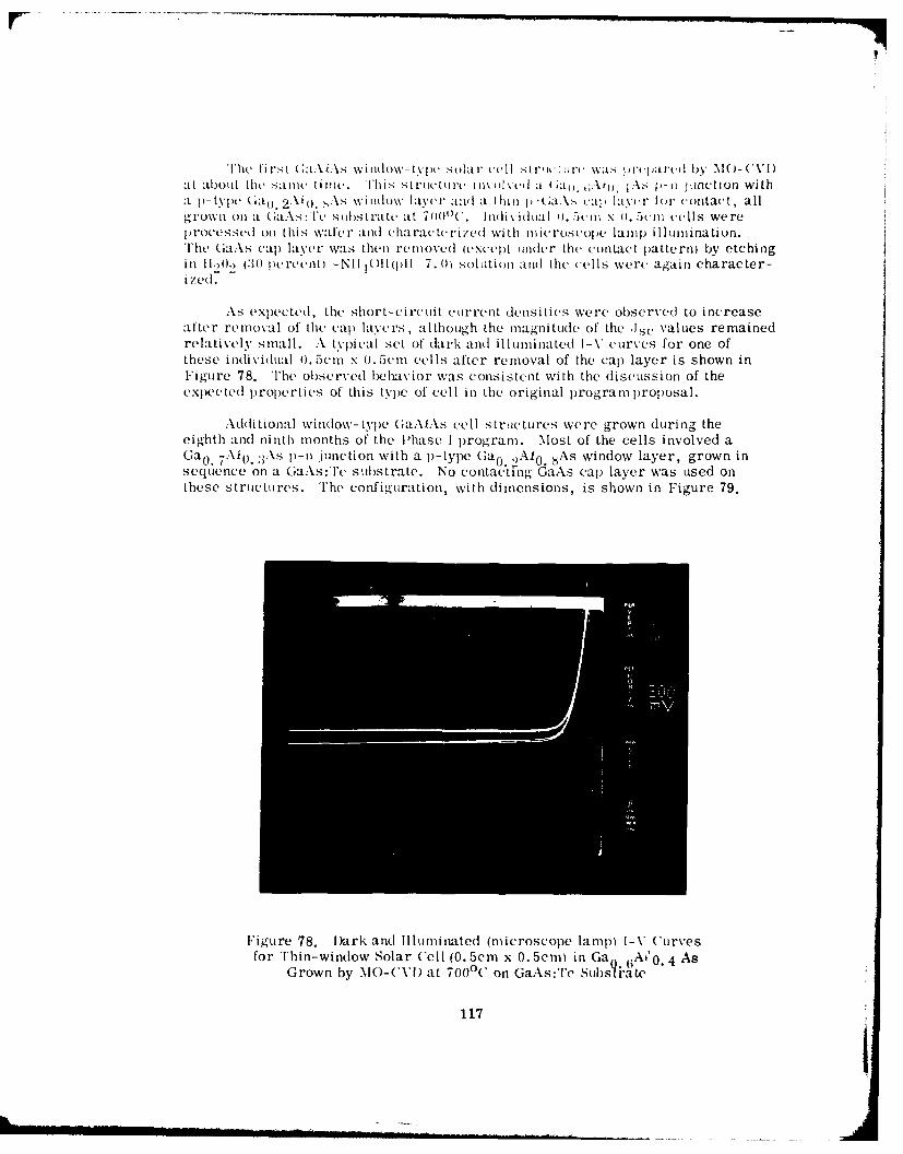
The fi I'81 (.aAiAs winth)V-tvlpt sola r cell st rt [Ire wvaS rj*(jared by M\O- ( \'ait about thet sain lin tli.Ti-; strutcturie m%1\ uvd a G(i;AoI.- p-ri junction witha P- tNype "ao 2 AiO AsWinditow laye r andI a phl 1-Ga.\s cat la ver for contact, allrow na as substrate at 7titt 1 (' indiv idual 0. 5Scml x o. 5cm cells were
p~rocessedl onl this wafer and charac ter ized wih in mic roscolpe lam p ill unination.'The GaAs cap) laver was then removed (except tinder the contact p~attern) by etchingin 1190O.) (30 percenit) -Nl 1 Ulltpil 7.O tsoIlutionl and the cells were again character-
As expected, thle short-ci rcunit current densities were observed to increaseafter removal of thle c-ap laye rs , although the magnitude of' the .C ~.Values remainedrelativelv small. A typ)ical set of' dark and il luminatedi I- \ c urves for one ofthese individual 0.5cmn x ). 5cm eel Is after removal of the capl layer is shown inFigure 78. The observetd behavior was consistent with thle discuIssion of theexpec ted prop~erties of this type of cell inl thle original program proposal.
Additional window- tyle GaAfAs c-ell strulctures were grown during theeighth and ninth months of thle P hase I program. Most of the cells involved aGa 0 . 7 kio. :;As p-n junction with a p-type Ga0 A10. As window layer, grown inseqluence onl a Ga..s:'l'e, substrate. No contaeting GaAs cap layer was used onthese structures. The config2uration, with dimensions, is shown in Figure 79.
Figure 78. D~ark and Illuminated] (microscope lamp) I-V Curvesfor Thin-window Solar Cell (0.5cm x 0.5cm) in Ga (AO 4 As
Grown by M0-CV) at 7000C on GaAs:Te Subs?I ate
117
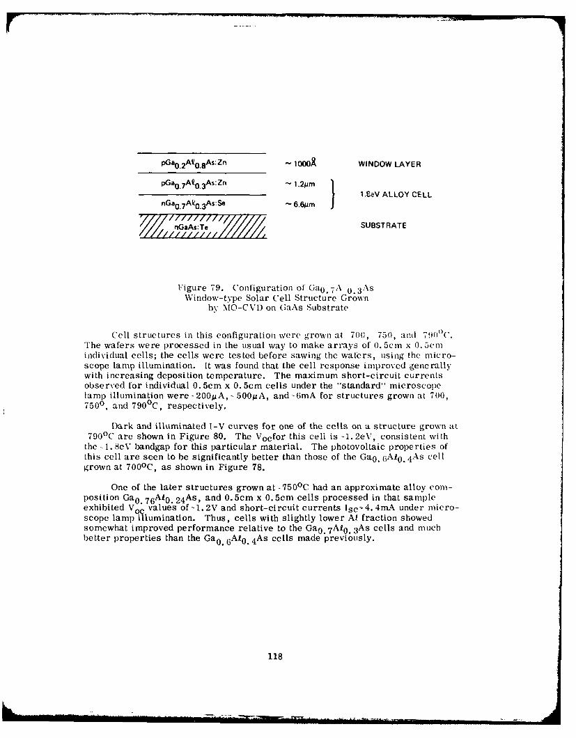
pGa 0 .2AV0. 8As:Zn - i000A WINDOW LAYER
pGa 0 .7AQ0 .3As:Zn - 1.2pm .I.SeV ALLOY CELL
nGa 0 .7 Ak0 ,3As: Se - 6.6pm J
nGAs:TeBSTRATE
Figure 79. Configuration of Ga 0 . 7 A 0 .:AsWindow-type Solar Cell Structure Grown
by MO-CVD on GaAs Substrate
Cell structures in this configuration were grown at 700, 750, and 790°)C.The wafers were processed in the usual way to make arrays of 0.5cm x 0.5C11individual cells; the cells were tested before sawing the waters, using the micro-scope lamp illumination. It was found that the cell response improved generallywith increasing deposition temperature. The maximum short-circuit currentsobserved for individual 0. 5cm x 0. 5cm cells under the "standard" microscopelamp illumination were-200pA,- 500pA, and-6mA for structures grown at 700,7500, and 790 0 C, respectively.
[)ark and illuminated I-V curves for one of the cells on a structure grown at790 0 C are shown in Figure 80. The Vocfor this cell is -1. 2eV, consistent with
the- 1.8eV bandgap for this particular material. The photovoltaic properties ofthis cell are seen to be significantly better than those of the Ga 0 . 6 A10. 4 As cellgrown at 700 0 C, as shown in Figure 78.
One of the later structures grown at-7500 C had an approximate alloy com-position Ga 0 7 6 A1 0 . 2 4 As, and 0.5cm x 0.5cm cells processed in that sampleexhibited Vo* values of-1.2V and short-circuit currents Isc-4.4mA under micro-scope lamp illumination. Thus, cells with slightly lower Al fraction showedsomewhat improved performance relative to the Ga 0 . 7 A10. 3 As cells and muchbetter properties than the Ga0. 6 A 0 . 4 As cells made previously.
118
6 L . . ... 1
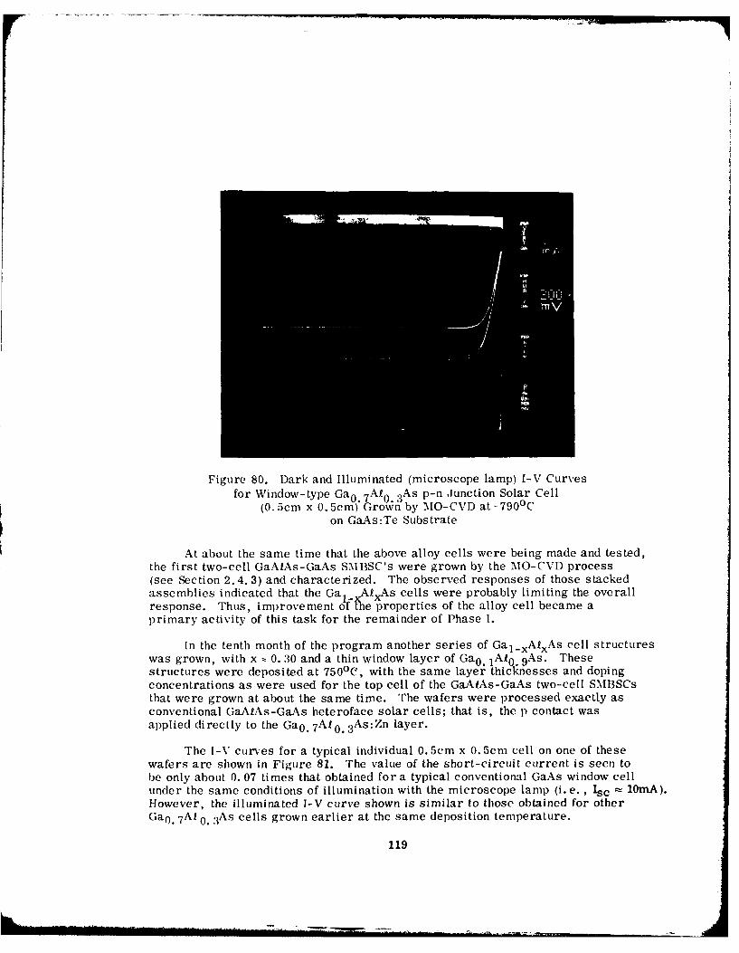
Figure 80. Dark and Illuminated (microscope lamp) I-V Curvesfor Window-type Ga 0 AI 0 3 As p-n Junction Solar Cell
(0.5cm x 0. 5cm) Grown by MO-CVD at- 790 0 Con GaAs:Te Substrate
At about the same time that the above alloy cells were being made and tested,the first two-cell GaAIAs-GaAs SMBSC's were grown by the MO-CVD process(see Section 2. 4. 3) and characterized. The observed responses of those stackedassemblies indicated that the Ga 1 xAIxAs cells were probably limiting the overallresponse. Thus, improvement off-'he properties of the alloy cell became aprimary activity of this task for the remainder of Phase I.
In the tenth month of the program another series of Gal-xAlxAs cell structureswas grown, with x , 0. 30 and a thin window layer of Ga 0 . 1A1 0 9 As. Thesestructures were deposited at 750 0 C, with the same layer thicknesses and dopingconcentrations as were used for the top cell of the GaAfAs-GaAs two-cell SMBSCsthat were grown at about the same time. The wafers were processed exactly asconventional GaMAs-GaAs heteroface solar cells; that is, the p contact wasapplied directly to the Ga 0 . 7 AI0. 3 As:Zn layer.
The I-V curves for a typical individual 0.5cm x 0. 5cm cell on one of thesewafers are shown in Figure 81. The value of the short-circuit current is seen tobe only about 0. 07 times that obtained for a typical conventional GaAs window cellunder the same conditions of illumination with the microscope lamp (i.e., lse - 10mA).However, the illuminated I-V curve shown is similar to those obtained for otherGa 0 . 7 A 0. 3As cells grown earlier at the same deposition temperature.
119
6oLl.. . . . .
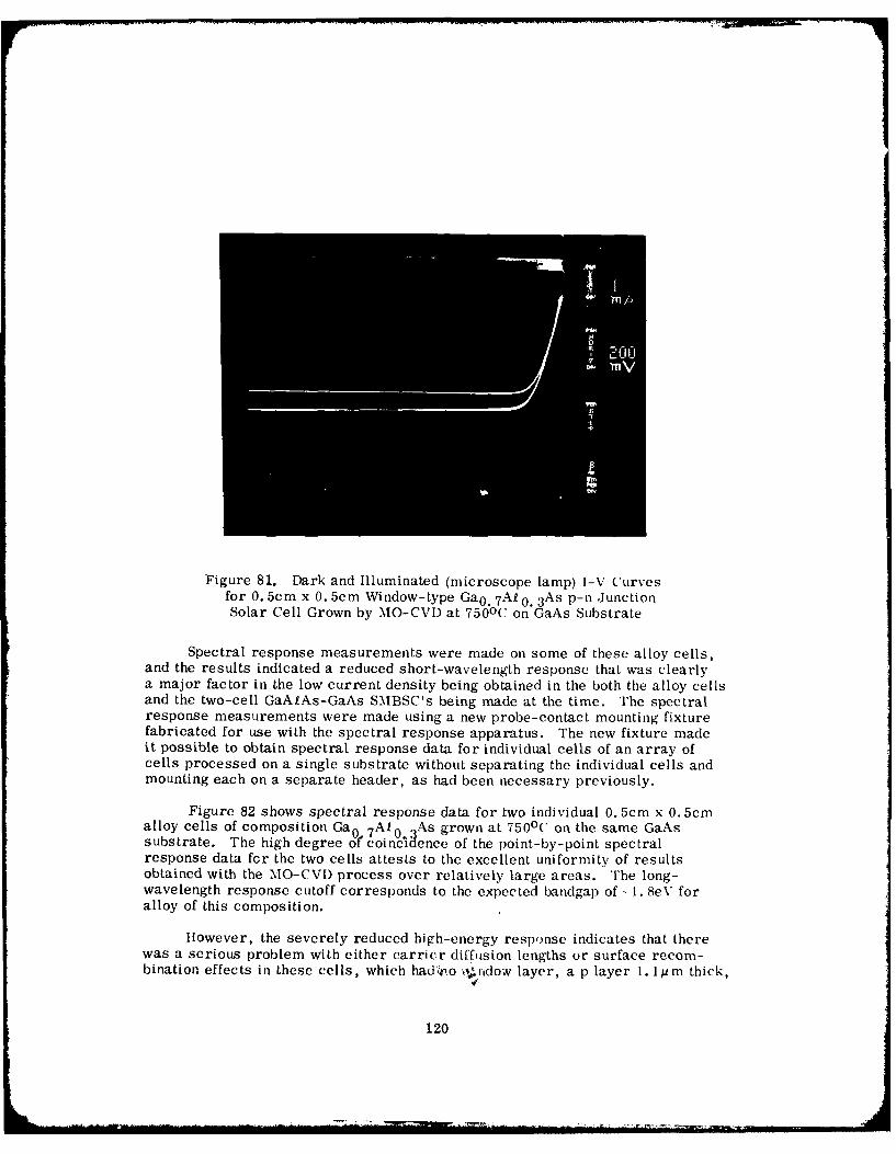
Figure 81. Dark and Illuminated (microscope lamp) I-V Curvesfor 0. 5cm x 0.5cm Window-type Ga 0 . 7 AI 0. 3As p-n JunctionSolar Cell Grown by MO-CVD at 7500C on GaAs Substrate
Spectral response measurements were made on some of these alloy cells,and the results indicated a reduced short-wavelength responsc that was clearlya major factor in the low current density being obtained in the both the alloy cellsand the two-cell GaAIAs-GaAs SMBSC's being made at the time. The spectralresponse measurements were made using a new probe-contact mounting fixturefabricated for use with the spectral response apparatus. The new fixture madeit possible to obtain spectral response data for individual cells of an array ofcells processed on a single substrate without separating the individual cells andmounting each on a separate header, as had been necessary previously.
Figure 82 shows spectral response data for two individual 0. 5cm x 0. 5cmalloy cells of composition Ga n 7 AI 0 2As grown at 750 0 C on the same GaAssubstrate. The high degree o' coincidence of the point-by-point spectralresponse data for the two cells attests to the excellent uniformity of resultsobtained with the MO-CVI) process over relatively large areas. The long-wavelength response cutoff corresponds to the expected bandgap of - 1. 8eV foralloy of this composition.
However, the severely reduced high-energy response indicates that therewas a serious problem with either carricr diffusion lengths or surface recom-bination effects in these cells, which hadhno N ndow layer, a p layer 1. 1 p m thick,
120
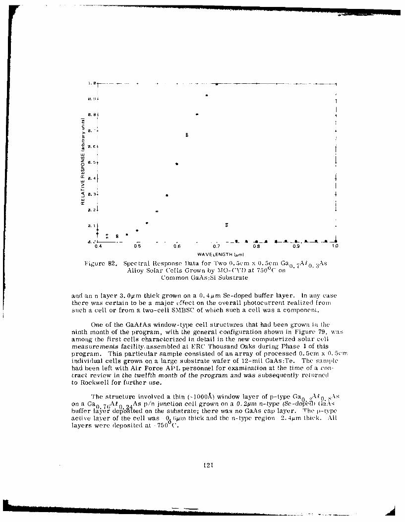
0.
CW
0 . E-J
w
>
o~0.
0. 1
0.4 0.5 0.6 0.7 0.8 0.9 1.0
WAVELENGTH (mm)
Figure 82. Spectral Response Data for Two 0.5cm x 0.5cma Ga0 7A 0 . 3AsAlloy Solar Cells Grown by MO-CVD at 7500 C on
Common GaAs:Si Substrate
and an n layer 3. 0pm thick grown on a 0. 4Mm Se-doped buffer layer. In any casethere was certain to be a major effect on the overall photocurrent realized fromsuch a cell or from a two-cell SMBSC of which such a cell was a component.
One of the GaAiAs window-type cell structures that had been grown in theninth month of the program, with the general configuration shown in Figure 79, wasamong the first cells characterized in detail in the new computerized solar cellmeasurements facility, assembled at ERC Thousand Oaks during Phase 1 of thisprogram. This particular sample consisted of an array of processed 0. 5cm x 0. 5cmindividual cells grown on a large substrate wafer of 12-mil GaAs:Te. The samnplehad been left with Air Force APL personnel for examination at the time of a con-tract review in the twelfth month of the program and was subsequently returnedto Rockwell for further use.
The structure involved a thin (-1000A) window layer of p-type Ga 0 k "10. s s"on a Ga0 7 ;Al 0 2 4 As p/n junction cell grown on a 0. 2pm n-type (Se-dolei) GaAsbuffer layer deposited on the substrate; there was no GaAs cap layer. The )-typeactive layer of the cell was -0. Gpin thick and the n-type region 2. 4pm thick. .l11layers were deposited at - 7500 C.
121
I Ii ~ l. . . ..., ...... A .
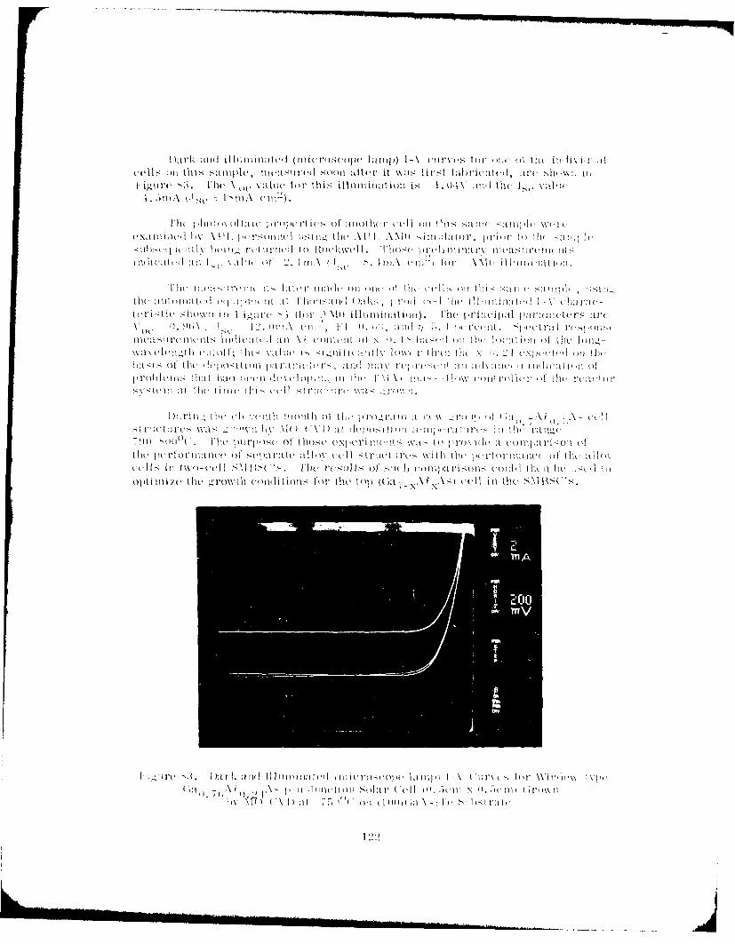
: ~~ce'lls (III this sattllle, tlw, .-u red, -,(()I ',tlte it % :,, I i t I tahric.:ttt+k, t'Ire -,),\m I it,
tigtire '3t. lh , x.tlu tilt this illumt itnation is I . I\ tlt thl 1..k, \ va ':It "ImA 0~m : I~w. c'~ )
I'l )11( )11 oi t I t:t w I i ij I I r t i tt ill' t m h i. (.. I ) ti II is -ta l n j )I(- wti rc&\V
ItI tI I' l I )v A Is I ,, li I I hc uAit I I x ) . i-i I'l IL , I w 11' (t h( in :i I l; tt ,
i'tt ll -it 1 1 1, hl tw IIlt t tt '(i1 IIt Il , ii , - in i ti iM i\ I tii S It I iit i
ci ett1 It 1it t I i/~i i ii it l i i ili i N i A is. I)I iw it l tii 1Aii ). it 1 In A % 1 11.li I ll t i 1tn t I .is t 11 11l .
11 I t li' l itu s 'it ;tlt ' :in ',, t,')It th l X) . I It it - I.X)(.:'I It I I I l' w( I Iw a t.\t l- 1, 11 c mt tl I' ; 1h1i< I\t , I ' iI t l ut i t I I I I , :t 1i:~ \1 it 1 It( ,l> .' ,1 i 1
)a I s ot[ .i I I :t I t it t I l t t t t ia rln( t , a l i I i i t t " 1tlN :1 11 :, \ :t ii .' , Iti 'li \ tui , ill (i
<v.' t 1) l t It(. I titb m tf i+ cc' I I rfi( + i f( 'A t P,< . ' t l .
I[ ) It ' i l i _ ' I t i .c t '("1 t h I + l l it. 1 1' ) ' t t 1 1 ( m 1P , % , 1 it W \ \ 1' ) 1 t " : l i t + % 7 i ; - < , l
T.l 1-l(( . lHiC 1-ltfl t 01 til~i t C NJ W I' II lltilt( " I n~'t < I i ih I l I >)),t -a' o III:I tIt Ili_ r 10 r I'l t (- (A",t'
+ I,' ! Il)'I I,.t ( ',ti V! t'(,Il - [ ' l~lt I W i * \\utI lt i l~ t l l'l. II( c r ( I Ic' '( ' i 'tilt-a lwI,
cet kl ill two'+-cc 'l .'I I. ".. I ~¢ V i ,( u ' - OJ .< 1 i I'} I) Q I 'I IrI,-;tm c~li~ I ll i -c 11 1 1 L' lt 1t 1 Wi
ol iti111 ze t he g rowvth1 c( ) titi t tit"oil r ct' t )p I ;: i -\X .-\A I' I Il in tihe+ S M ,,I S .
i
I* ( ' i -I U I 1:t ill 1\-1 I - ill tI ~I i" th 'll m . I t .I l r Wl I I I I I 12•~ ~ ~~~~~~~ li,, "(11. ('\ 1:1 )(.-Ill
' l IIt I.;l ['(I' 1'1'< l;l
111, 17 T .-I I I ' ' ( ~I l2 I \.:2 I:I
B1
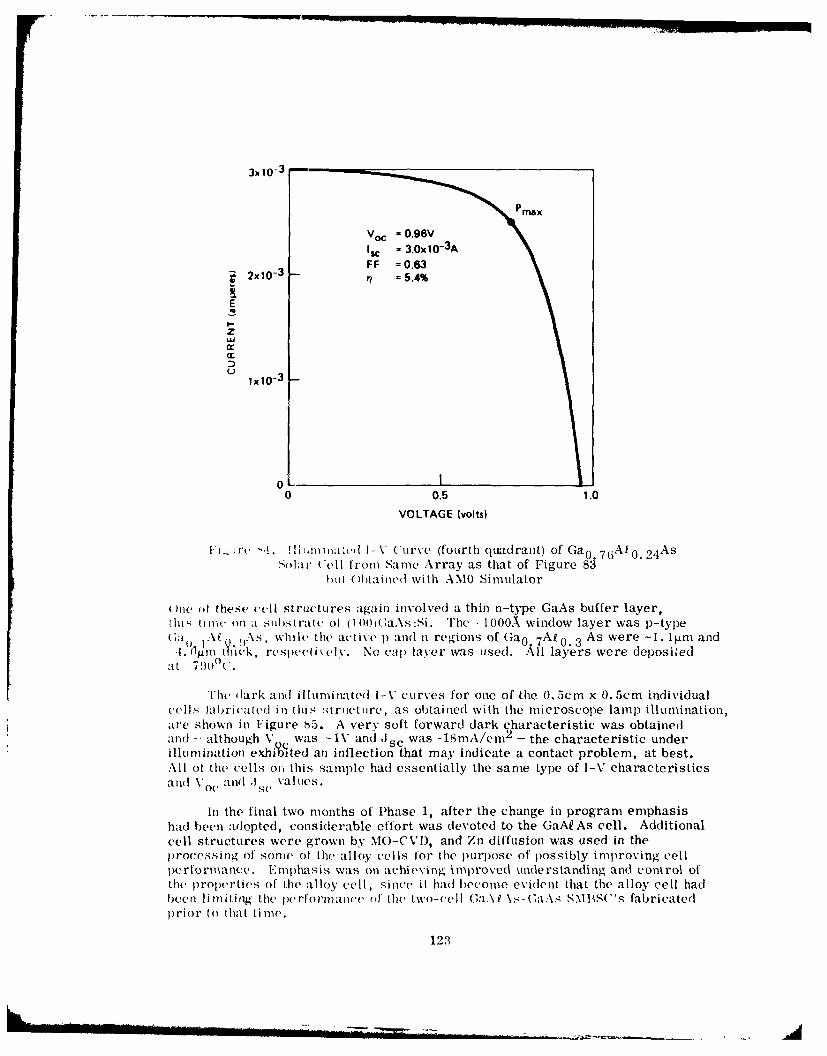
3-10-
Pmax
Voc = 0.96VIsc = 3.0x0- 3 A
FF = 0.63T2x10 3 - = .4%1i
E
z
Dlx10-3
0 L
0 0.5 1.0VOLTAGE (volts)
[. r. ",4. 'lj mi'a:.ell 1-V ('urvC (fourth quadrant) of Ga 0 . 7 6 A 0. 2 4 AsSolar (ell from Same Array as that of Figure 83
hut ()htained with AMO Simulator
()ne (it these cull structures again involved a thin n-type GaAs buffer layer,t Uhis (I Inc o a1 su)strate of (1 00 )(aAs:Si. The - 1000A window layer was p-type;aO ,\O ,\ s, while the active p and n regions of Ga 0 7 A 0 .3 As were -1. lp.m and1. dthi fk, respectivclv. No ear laYer was used. All layers were deposited
at 790o(.
'he, (lark and illuminated I-V curves for one of the 0.5cm x 0.5cm individualcells labricated in this 'trtuture, as obtained with the microscope lamp illumination,are shown in Figure 65. A very soft forward dark characteristic was obtainedand - although V c was -IV and J was -18mA/em 2 - the characteristic underin( - o,..h caateitc neillumination exhiited an inflection that may indicate a contact problem, at best.All ot the cells on this sample had essentially the same type of I-V characteristicsand Vo. and .1 sC values.
In the final two months of Phase 1, after the change in program emphasishad been adopted, considerable effort was devoted to the GaAe As cell. Additionalcell structures were grown by MO-C(V), and Zn diffusion was used in the)rocessing of sonc of Ihe alloy cells for the purpose of possibly improving cell
performance. 'mphasis was on achieving improved understanding and control ofthe properties of the alloy cell, since it had become evident that the alloy cell hadbeen l imiting the performance of the two-cell GaA \ s- GaAs SMBS("s fabricated)rior to that tinm,.
12:3
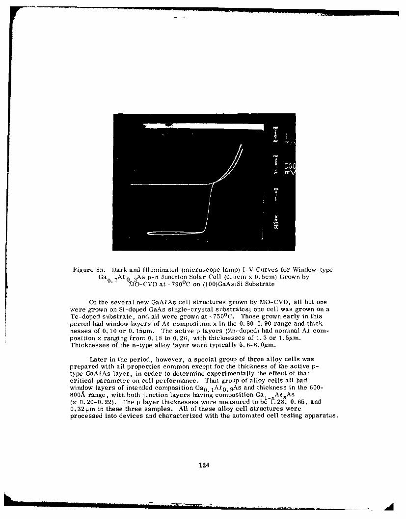
Figure 85. Dark and Illuminated (microscope lamp) I-V Curves for Window-typeGa 0.7 A 0 . 3As p-n Junction Solar Cell (0. 5cm x 0. 5cm) Grown by
Nf0-CVD at - 790 0 C on (100)GaAs:Si Substrate
Of the several new GaAfAs cell structures grown by MO-CVD, all but onewere grown on Si-doped GaAs single-crystal substrates; one cell was grown on aTe-doped substrate, and all were grown at -750 0 C. Those grown early in thisperiod had window layers of Al composition x in the 0. 80-0. 90 range and thick-nesses of 0. 10 or 0. 15m. The active p layers (Zn-doped) had nominal At com-position x ranging from 0.18 to 0.26, with thicknesses of 1. 3 or 1. 5m.Thicknesses of the n-type alloy layer were typically 5. 6-6. Opm.
Later in the period, however, a special group of three alloy cells wasprepared with all properties common except for the thickness of the active p-type GaAIAs layer, in order to determine experimentally the effect of thatcritical parameter on cell performance. That group of alloy cells all hadwindow layers of intended composition Ga 0 . 1 At0. 9As and thickness in the 600-800A range, with both junction layers having composition Ga AilAs(x 0. 20-0. 22). The p layer thicknesses were measured to be l. 28, 0. 65, and0.32xm in these three samples. All of these alloy cell structures wereprocessed into devices and characterized with the automated cell testing apparatus.
124
The alloy cells previously made by MO-CV), whether separate cells or partof a two-cell SMIBSC with GaAs, generally exhibited very low .sc values - typically<5mA./cm 2 for AMO illumination. l'hotoresponse measurements had indicatedthat the electron diffusion lengths in the 1) layers were probably less than thejunction depths, so that relatively poor collection efficiency, especially evidentat short wavelengths, had resulted. The group of three alloy cells referred toabove was prepared specifically to investigate this problem. Those cells togetherwith the other alloy cells grown and evaluated in the final two months are listed inTable 8, which shows the principal physical parameters of the structures.
Also listed are two other alloy cells grown by MO-CVI) earlier in the program,one of which (AB90526A) was characterized in detail with the more recent cells.The other, listed for comparison only, is the alloy cell (A390427A) discussedearlier and represented in Figures 83 and 84.
The measured photovoltaic properties of the alloy cells listed in Table 8are given in Table 9, as determined with AMO simulated illumination (FLtt lamp)in the automated facility. The AR content x in the p and n junction-torminglayers of Gal_xA2xAs of each of the cells was deduced from the location of thelong-wavelength cutoff in the measured spectral response cur,,, based onthe published bandgap-composition data of Panish (Ref 13).
The tabulated results show that the open circuit voltage Voc of the cellincreases as the Al cont.tit of the junction-forming alloy increases. The measuredrange of variation of Voc with the deduced Al content in the junction layers for thesecells is plotted in Figure 86, along with a reference plot (linear) of expected band-gap in the junction region as a function of Al content. Trhe observed increase inV with deduced Al content is considerably slower than the linear variation ofbandgap with Al content until Al compositions 0. 30 are reached, and the Vocvalues at all but the lowest Al compositions (i.e., for GaAs rather than GaAtAscells) are significantly less than the expected values. In fact, there is relativelylittle increase in V with Al content of the junction layers until x exceeds - 0. 2.Some of the alloy cefls had relatively low short-circuit current densities as aresult of junctions that were too deel) (i. e., p-type active regions too thick), so theproblem of the low Voc values could be reduced somewhat as the alloy cell designis optimized. However, further work is clearly needed in order to improve theV oc values and thus realize the potential peak efficiencies of which these devicesshould be capable.
The short-circuit current density Jse obtained with these cells depends uponboth the Al content and the thickness of both the window layer and the junctionlayer. The variation of Jse with thickness of the p-type alloy layer (i. e.,junction depth) for the group of three cells grown with p layer thicknesses of1.28, 0. 65, and 0. 32;m is shown in Figure 87. It appears that increasing thejunction depth from - 0. 3 to 0. 7pm had little effect on J-c but further increaseto - 1.3Mm produced a major reduction in the collected sgort-circuit currentdensity. This result suggested a minority carrier diffusion length of - 0. 5pm forthis material, indicating that a shallow-junction structure (i. e., _<0.5pm) is neededfor optimized performance for the alloy cell.
'125
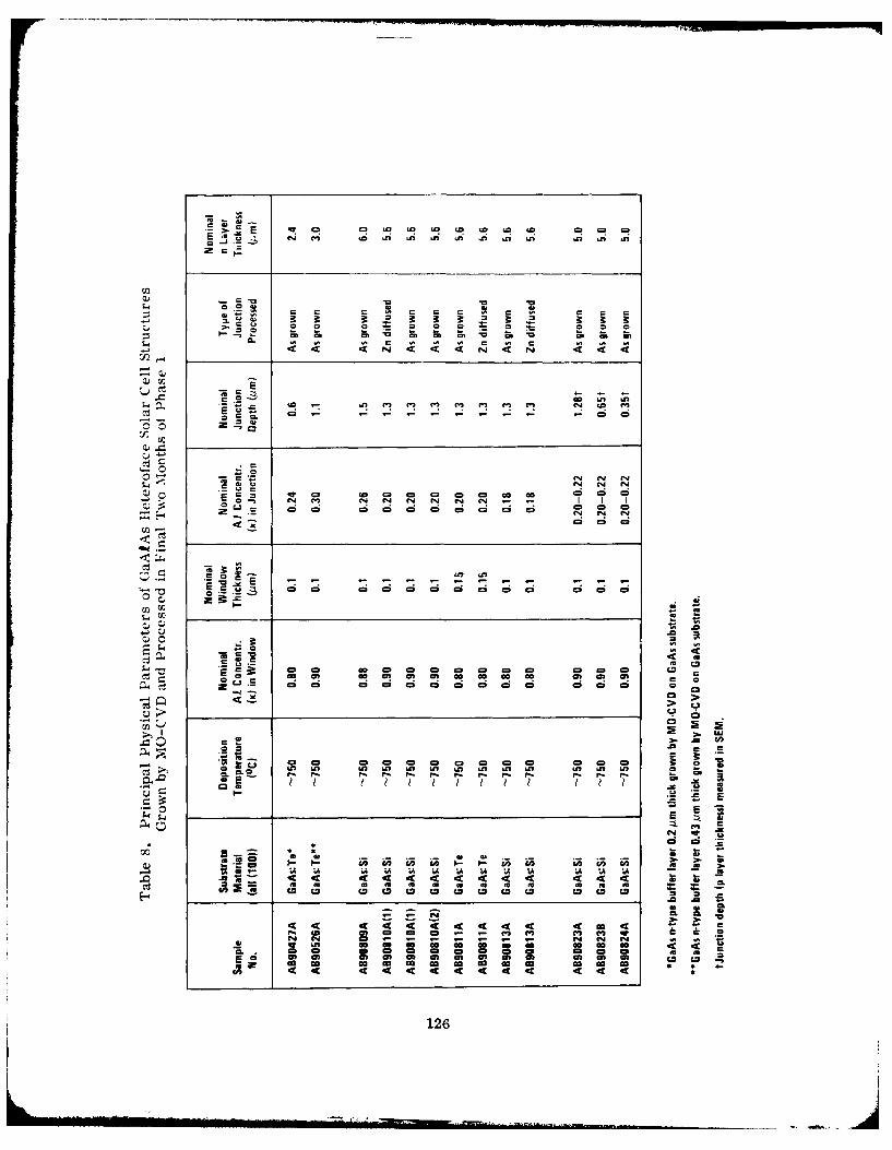
N ' 0 U, U, U, U, U, U, U, U, U U,C n t n L n In I n I n I
U2
-. -
'-4D
ci 5
C43 C) CID CD ~ ' ' ') C) C) N 4
c-4 N I I
r= -a N
S0 C3 CD C Cm cm 0 c40C
EP U
~ .~ o' - - - -
0* :-
o ~ ~~ ~ ~ ~ cm C oUD4 )Cd ~ ~~~~~~~~~~ I n D G $c c cc o a "c
L) c
0 SC C;C C) C) C
4-54
4 < 1 dcr._____ C.3
c w 0 0 C C C C CU, U U) U, U U, U, U U, U, U U, UM
C'S .. S I' C' 4.. C'- I'S 4. C. IS C' I'SC-
1~c c" -0 1 1 -
1262
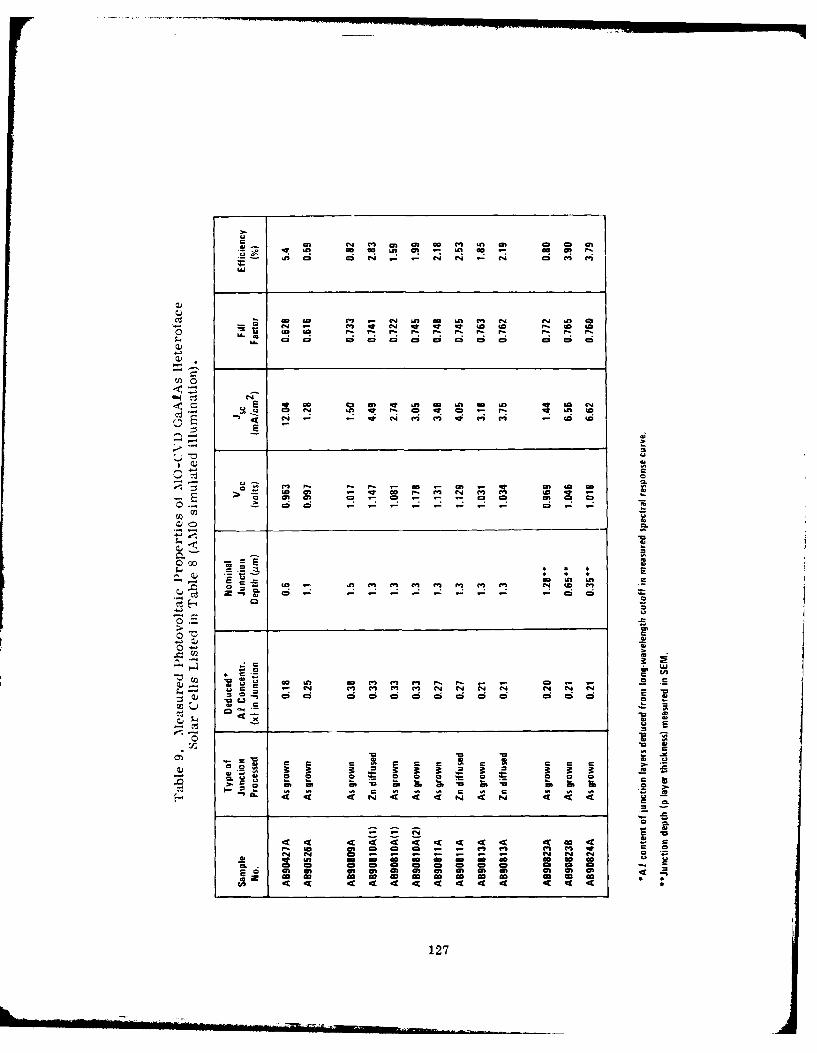
La
L 0 n a n M r4 In - D
-. m 0 ~ , -C"1 mr qt w~ w. 10 0to cc ('I rZ (Nr-10 1 -ur(u 10 1 . r% pl . p: p. rp. p. .
( N. : ! mN ( ' I (U1 r 4~ 9-
Icr,
C2 -. -. - - - -, - - , 1
0 00a -0 0 a
0 77
vi Ili zi
I n 0D w 0 En mCLa
In_ a,,Iam cc
C3 14
~ 127
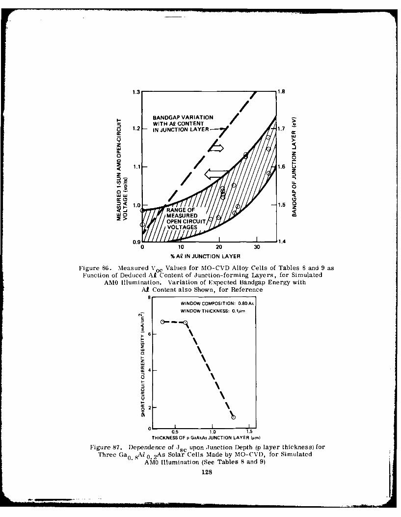
1.3 1.8
BANDGAP VARIATION12 WITH AR CONTENT I .
1. IN JUNCTION LAYER-1.7Ew
z
1. 1.6 L)z
-L 0
LU LU
c1. 0
MEASURED .
OPEN CIRCUIT
0.9 '1.40 10 2030
% AR INJUNCTION LAYER
Figure 86. Measured V Values for MO-CVD Alloy Cells of Tables 8 and 9 asFunction of D~educed At Content of Junction-forming Layers, for Simulated
AMO Illumination. Variation of Expected Bandgap Energy withAt Content also Shown, for Reference
WINDOW COMPOSITION: 0.80Ak
WINDOW THICKNESS: 0.1tim
E
U)
UA
z
Uc-
W 4
cc128
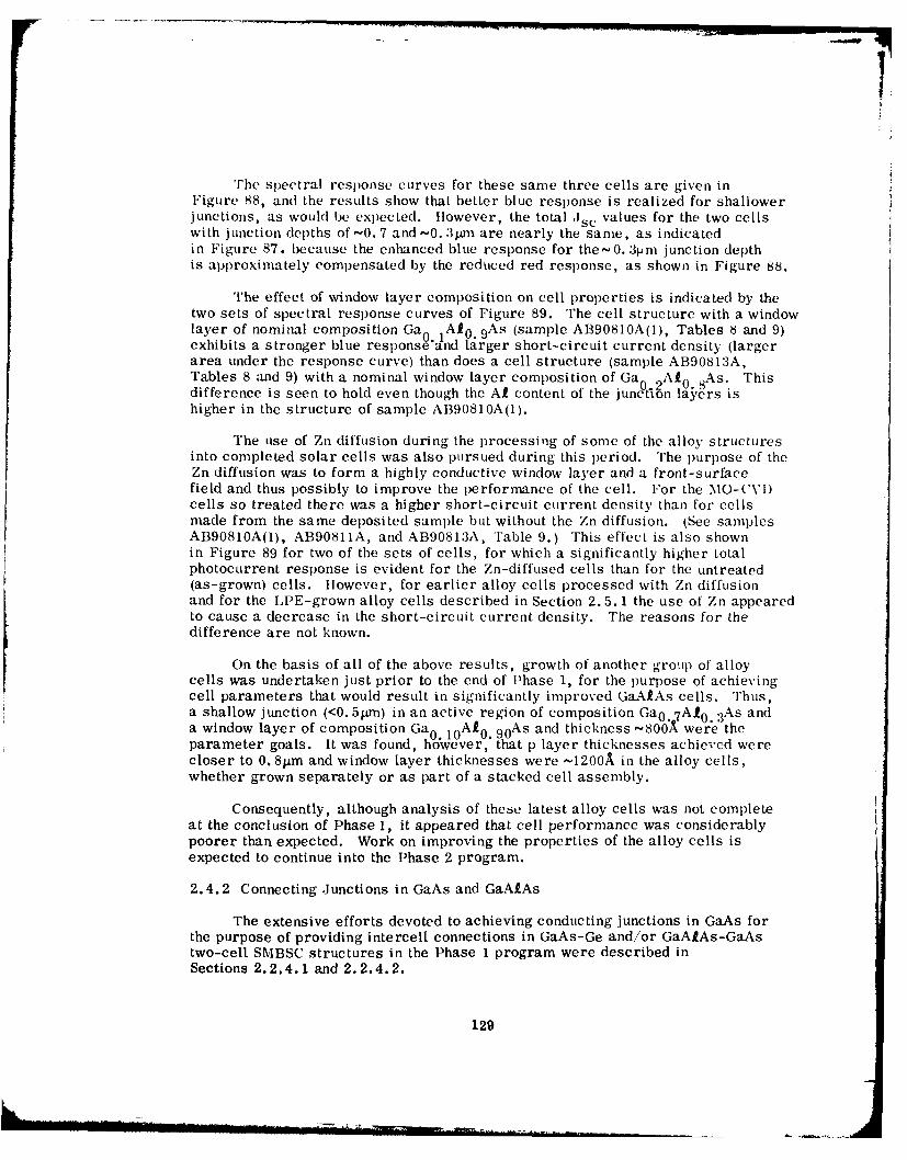
I
The spectral response curves for these same three cells are given inFigure 88, and the results show that better blue response is realized for shallowerjunctions, as would be expected. Iowever, the total Jsc values for the two cellswith junction depths of-0. 7 and -0.3m are nearly the same, as indicatedin Figure 87. because the enhanced blue response for the-0. 3pm junction depthis approximately compensated by the reduced red response, as shown in Figure 88.
The effect of window layer composition on cell properties is indicated by thetwo sets of spectral response curves of Figure 89. The cell structure with a windowlayer of nominal composition Ga 0 _A1 0 9 As (sample AB90810A(1), Tables 8 and 9)exhibits a stronger blue response and larger short-circuit current density (largerarea under the response curve) than does a cell structure (sample AB90813A,Tables 8 and 9) with a nominal window layer composition of Ga 0 2 Al 0 8 As. Thisdifference is seen to hold even though the Af content of the junction layers ishigher in the structure of sample AB90810A(1).
The use of Zn diffusion during the processing of some of the alloy structuresinto completed solar cells was also pursued during this period. The purpose of theZn diffusion was to form a highly conductive window layer and a front-surfacefield and thus possibly to improve the performance of the cell. For the MO-C'VI)cells so treated there was a higher short-circuit current density than for cellsmade from the same deposited sample but without the Zn diffusion. (See samplesAB90810A(l), AB90811A, and AB90813A, Table 9.) This effect is also shownin Figure 89 for two of the sets of cells, for which a significantly higher totalphotocurrent response is evident for the Zn-diffused cells than for the untreated(as-grown) cells. However, for earlier alloy cells processed with Zn diffusionand for the LPE-grown alloy cells described in Section 2.5. 1 the use of Zn appearedto cause a decrease in the short-circuit current density. The reasons for thedifference are not known.
On the basis of all of the above results, growth of another group of alloycells was undertaken just prior to the end of Phase 1, for the purpose of achievingcell parameters that would result in significantly improved GaAAs cells. Thus,a shallow junction (<0. 5pm) in an active region of composition Ga 0 7 A210 .As anda window layer of composition Ga n 10 A. 0 9 0 As and thickness -800A were theparameter goals. It was found, however, that p layer thicknesses achieved werecloser to 0. 81am and window layer thicknesses were -1200A in the alloy cells,whether grown separately or as part of a stacked cell assembly.
Consequently, although analysis of these latest alloy cells was not completeat the conclusion of Phase 1, it appeared that cell performance was considerablypoorer than expected. Work on improving the properties of the alloy cells isexpected to continue into the Phase 2 program.
2.4.2 Connecting Junctions in GaAs and GaAfAs
The extensive efforts devoted to achieving conducting junctions in GaAs forthe purpose of providing intercell connections in GaAs-Ge and/or GaAIAs-GaAstwo-cell SMBSC structures in the Phase 1 program were described inSections 2.2.4.1 and 2.2.4.2.
129
7-
S0.613p m6
- - 0. 35,u
>4I;-
z
I- 1-W
_.1-jw
4000 5000 6000 7000 8000 9000
WAVELENGTH (A)
Figure 88. Spectral Ilesponse Curves for Three MO-('V) Ga 0 .S At 02As (ells
of [)ifferent ,function Depths () layer thickness).
(See Tables 8 and 9 and Figure 87)
7
6 SAMPLE AB90813AC Ga0 2A 0 .8 As WINDOW (0.1m THICK)
-5 -- SAMPLE AB9 81OA (1) .a0 79 A0.2 1A JUNCTION
-Ga0.1A0.gA WINDOW (0.1/m THICK)" 4 Ga0 6 7A 0 .33As JUNCTION>. 4 0.6I-z DIFFUSEDU,,zI-
Z Zn DIFFUSEDz> 2
AS GROWN A
W 1 GROW
04=0 5W0 6000700a
WAVELENGTH (A)
Figure 89. Spectral Photoresponse C(trves for GaAfAs Solar Cells Made in
MO-CVI) Structures laving Different GaAgAs Window-layer Compositions
(and different junction- layer compositions), Processed
Both in As-grown Condition and with Zn I)iffusion
130
Consequent ly, the discussion in this section is confined to a description ofthe efforts to achieve tunneling junctions in GaAfAs, for use in connecting GaAIAsand GaAs cells in two- or three-cell SMBS ' structures.
The first GaA-As junction structures grown with doping concentrationsintended to produce tunneling characteristics were prepared in the third andfourth months of the program. Several n+i p+ Ga At As structures with x-0. 37were deposited by MO-CVI) on GaAs substrates a[t-7506C. None of those firststructures grown in this configuration exhibited tunneling properties, however.
Evaluation of the properties of the first few unsuccessful structures providedthe information needed to identify deposition conditions that did result in tunnelingproperties. The experiments with GaAs tunneling junctions (Section 2.2.4.1) hadshown that lower deposition temperatures than those normally used for GaAs filmgrowth by the MO-CV1) process were required for achieving tunneling characteristics.Consequently, single layers of GaAfAs alloys were grown on GaAs substrates at-700(' to establish alloy compositions of layers grown und]er selected conditions.The alloy composition was determined by x-ray double-crystal diffractometermeasurements and - for alloy films with compositions in the direct-bandgal) range -by room-temperature photoluminescence measurements. It was found that alloycoml)osition is not strongly dependent upon deposition temperature for a given setof other )arameters in this range. That is, the dependence of the x value on theTMAI:TMG partial-pressure ratio during film growth agreed well with thatdetermined in earlier studies using different deposition conditions (especiallyteml)erature).
l)uring the eighth month of the program a Ga 0 9)A1 0 0%s p n- el)itaxialstructure was grown by MO-CVI) at 7000 C on a GaA s:Si substrate, as the nextstep in identifying the deposition conditions required for producing a tunnel diodestructure in this material. Preliminary evaluation of this sample using In con-tacts and the mechanical probe indicated a weak tunneling characteristic.lowever, when individual mesa diodes were fabricated with ohmic contacts theevaluation showed a heavily doped back-to-back diode characteristic but notunneling behavior.
Despite this unsuccessful result, two-cell SMBSC structures each consistingof a Ga0 (iAl 0 4 As p-n junction cell and a GaAs p-n junction cell grown sequentiallyon a Gais:Te substrate, with the two cells connected by an n+p+ junctionstructure, were grown entirely by the MO-CVI) process. One such SMIBSCstructure had the n+/p+ junction in the GaAs (see Section 2.2.4. 1), and the otherhad the n+/p+ junction in an alloy double layer of composition Ga 0 2 A10. 0 8 As.The configuration of this structure was as shown schematically in'R*gure 90.
Characterization of the resulting structure, as described in Section 2.4.3,indicated that the junction (lid not have tunneling properties, despite the fact thatthe doping concentrations on both sides of the junction were believed to be veryhigh.
,The lack of clear-cut success in achieving good tunneling properties in n 4+=junction structures in GaAfAs resulted in attention being shifted to the formationof the req(uired connecting junction structures in GaAs, for which success had
131
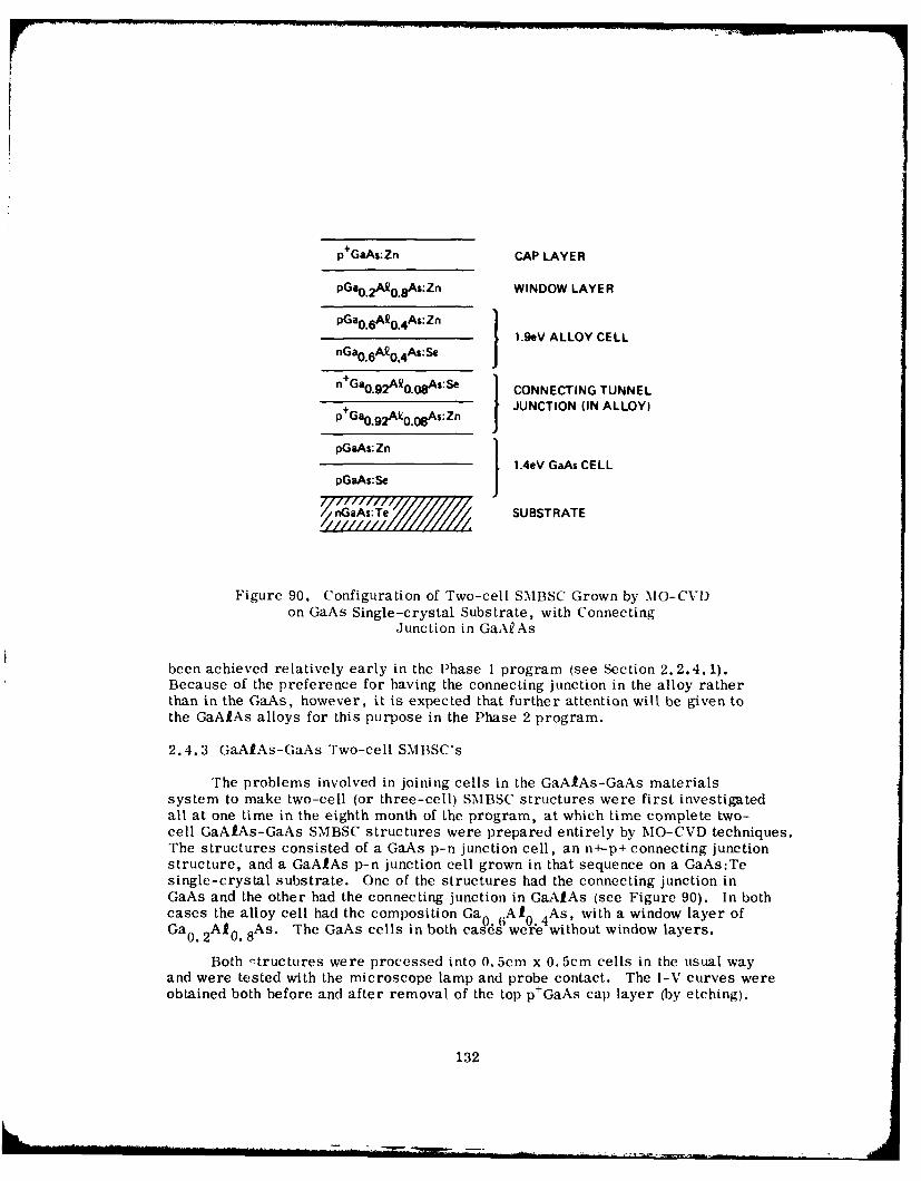
p +GaAs.Zn CAP LAYER
PGao.2 AR0.8 As:Zn WINDOW LAYER
pGa 0.6A10 .4As: Zn1.9eV ALLOY CELL
nGa0.6A' 0 ,4 As: Se Jn +Ga0 .9 2A20 "08As:Se CONNECTING TUNNEL
p+Ga9A Zn j JUNCTION (IN ALLOY)
pGaAs: Zn11.4eV GaAs CELL
pGaAs:Se
A:T e SUBSTRATE
Figure 90. Configuration of Two-cell SMBSC Grown by MO-CVDon GaAs Single-crystal Substrate, with Connecting
Junction in GaA2As
been achieved relatively early in the Phase 1 program (see Section 2.2.4.1).Because of the preference for having the connecting junction in the alloy ratherthan in the GaAs, however, it is expected that further attention will be given tothe GaAIAs alloys for this purpose in the Phase 2 program.
2.4.3 GaAlAs-GaAs Two-cell SMBSC's
The problems involved in joining cells in the GaAlAs-GaAs materialssystem to make two-cell (or three-cell) SMBSC structures were first investigatedall at one time in the eighth month of the program, at which time complete two-cell GaAfAs-GaAs SMBSC structures were prepared entirely by MO-CVD techniques.The structures consisted of a GaAs p-n junction cell, an n+-p+ connecting junctionstructure, and a GaAlAs p-n junction cell grown in that sequence on a GaAs:Tesingle-crystal substrate. One of the structures had the connecting junction inGaAs and the other had the connecting junction in GaAIAs (see Figure 90). In bothcases the alloy cell had the composition Ga 0 At .4 As, with a window layer ofGa0. 2 At 0 . 8 As. The GaAs cells in both cases were without window layers.
Both ctructures were processed into 0.5cm x 0. 5cm cells in the usual wayand were tested with the microscope lamp and probe contact. The I-V curves wereobtained both before and after removal of the top p+GaAs cap layer (by etching).
132
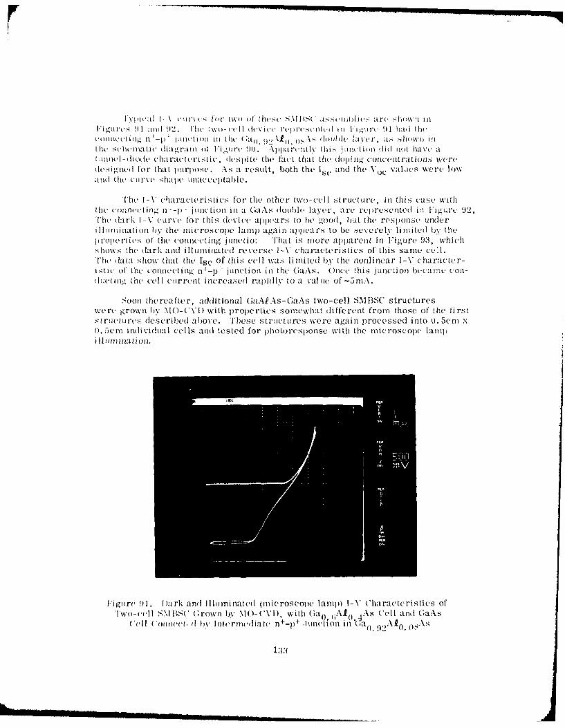
I \licLl - \cul\ hafu tkvO (d, thesew SM.\l lt( a.ssclllhfis are swnInIIigmits 91 am!i 92. Ill two- cli device eFseti ill fiue91 haid thecoinnctIn. n -p' junction in the. "0 92"K Wkl \s' 1fonle laYer-, as 'hwnI'the selieniatic i grain ()f Iigui' 9U. Afpi ur i't lt th is j u i L ii)n d nI ot ha ve ahiiiclef-diode characteristic , (((-spite the f-act thait the dloinrg c'onlcntrationis were
designed f'or that purpose . As a result, both the IS and the VO val'ies were lowkanid the curve shape unaceefitahle.
The 1-V characteristics for the other tw-cell strmure , ini this case iththe coinelf till)f fI j inchton ini a Gai.s (o101)T, layeri, arie rep rese nted in Figure 92.
iThe drk I -V enr" I'e o this device appea rs to he good, but the response underill urn hntion by the microscope lamplf agan a i ia rs to be sevrely lMite by thepr'operties of' the connecting jnrcti 1l'at is more apparent in Figure 93, whichs hows the (lark and illurnrated reverse I-V characteristics of this same cel.T'he data show that the Ise of this cell was li mited by the nonlinear l- V character-Ist ic of' the connecting nA--p: junction in the GaAs. Once this j One ton became con-if lt ig -; the cell cunrrent increased raqjidl" to a Wvl e, of -'5mnA.
Soon thereafter, additional GaAP As-GaAs twNo-cell SMNBSC structureswere grown by MO-C(VI) with proprerties somewhat different f'rom- those of the fi rststructures described above. These structures were again processed into 0. 5cm x0. 5cmi individuial cells and tested for photoresponse with the microscope larl)ilIluminati on.
F'igu re 91I. D a rk and Illuminated (microscope lamp) 1- V ('harac te ristics ofIwo- eel I SNI BS(' Grown by () (X) with Gao 1.AI (.\s ('el and GaAs
('elI (Con nectifby Inrie rmed iate fl-Jp+ .1ulne ti on in a 0 ,9 A().* 0. S' 5
N13 :-
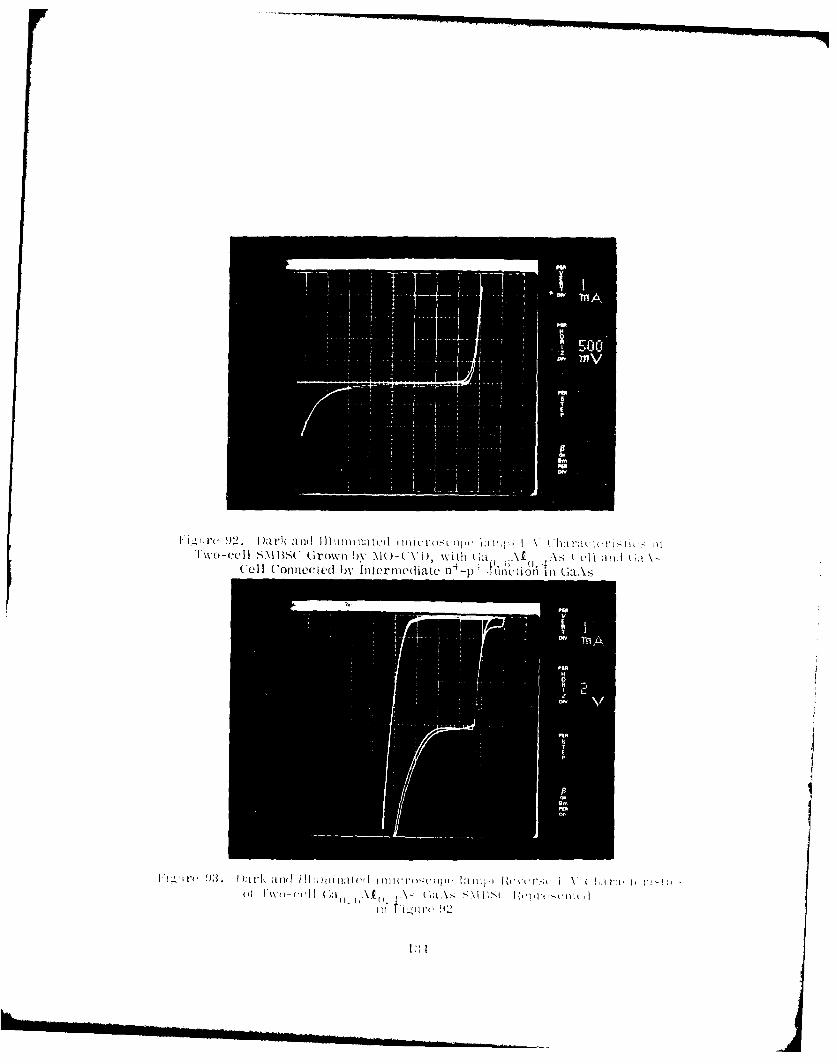
Ywo-ecou S\IBS( Grown 1)v ()(I, With (;:L \k - k :n ~\Cell C(onnect[ed by 'Intermediale fl-p 1.1i Lo'iII 3~
9:3. ~ ~ ~ ~ ~ n 111fliie oico,(k (,l m i hnL~
GI V S~l,.,I
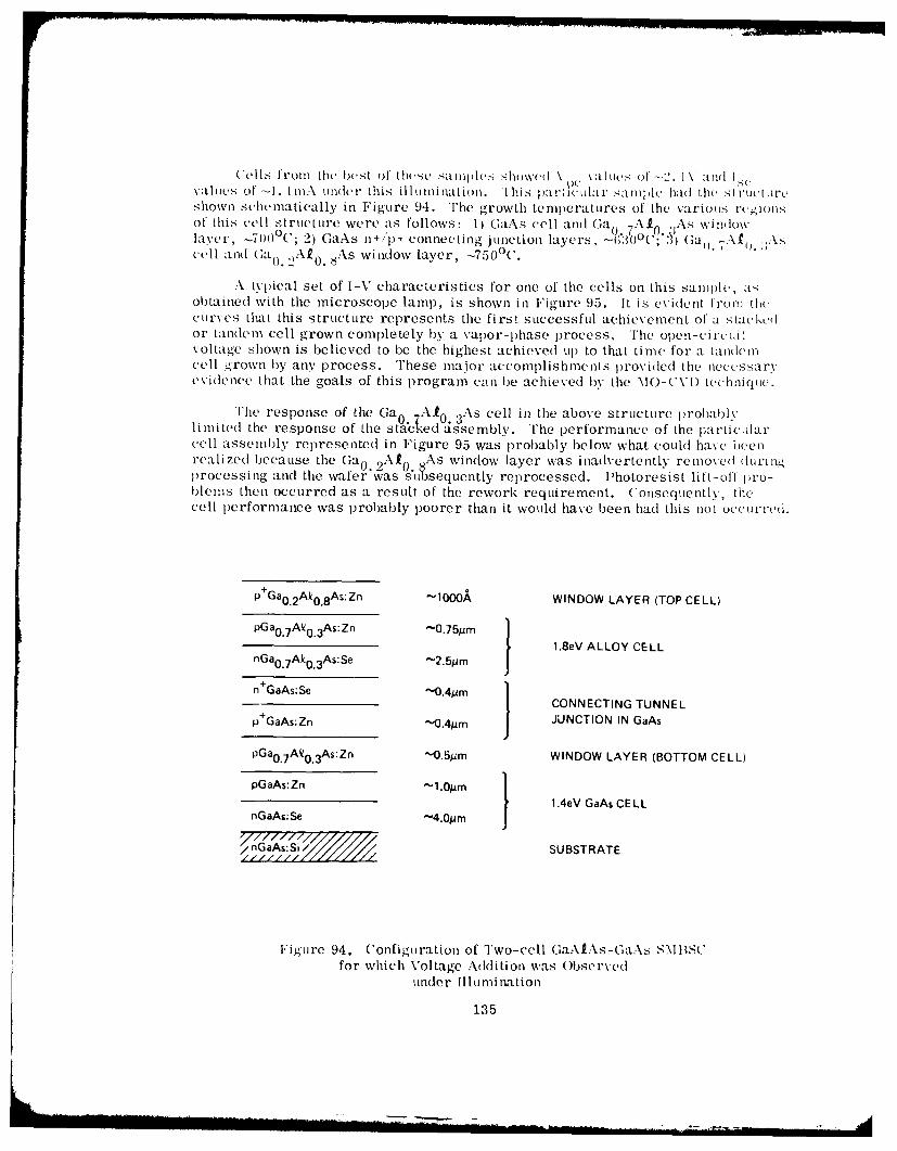
Cells fromi the hest of' these simples sho% ed \ 1 \lI uc of --L!. I 1 liad I SvalIutes ofl -. I miA itnkcr this iIlI UIn IIinatin. Ihis atI I Z1 ar11,1 samlple had the stliwetircshown schemiatically in Figure 94. TIhe growth temperatures of the various re 'ionsof' this cell Structure Were as follows: 1) Ga.Ns cell and Ga 1 I As winidowlayer, --700o('; 2) GaAs n±"'p - connecting junction layers, 4('1 V Ga -7,k Ascell an(I Ga. 2 As window layer, -~7500('.
A tvypical set of I-V characteris tics for one of the cells on this sample, ta;obtained wvith the microscope lamp, is shown in Figure 95. It is eVide nt froll thccutrves that this structure represents the first Successful achievement of' a ta Ikeor tandlem cell grown completely by a vapor-phase process. The open-cri Lvoltagre shown is believed to be the highest achieved up11 to that time for a tandemcell gorown by any process. TIhese major accomplishments providecd the necessary'evidence that the goals of this program can be achieved by the \lO-CVD I)echnique.
J'he response of the Ga 7 AID .,As cell in the above structure probalvlimited the response of the stackedtiassembly. [heli performance of the particidlarcell assembly represented in Figure 95 was probably below what could have beenrealized because the Ga 0 NAI As window layer was inadvertently removed lu1.ring"processing and the wafer'was SUsequently reprocessed. 1~hotoresist lift-off pro-blems then Occurred as a result of' the rework requirement. Consequently, thecell p~erformance was probably poorer than it Would have been had this no0t oc-Curred.
p+ Ga0 2Ako.8 As:Zn -1000A WINDOW LAYER (TOP CELL)
PGa. 7 Ak0 .3 As:Zn -0.75pm
n~a.7kO.AsSe 2.; I 1.8eV ALLOY CELL
n+GaAs:Se M'0.4pm 1j CONNECTING TUNNEL
p+GaAs;Zn J-.4u JUNCTION IN GaAs
pGa0 .7AVO 3As:Zn -05mWINDOW LAYER (BOTTOM CELL)
PGaAs:Zn -l.0Am
n~a~:Se 4.0jm I 1.4eV GaAs CELL
~s~Si/SUBSTRATE
Figure 94. C'onfiguration of 'iwo-cell GaAfAs-GaAs S,\IBSCfor which Voltage Addition was Observed
under Illumination
135
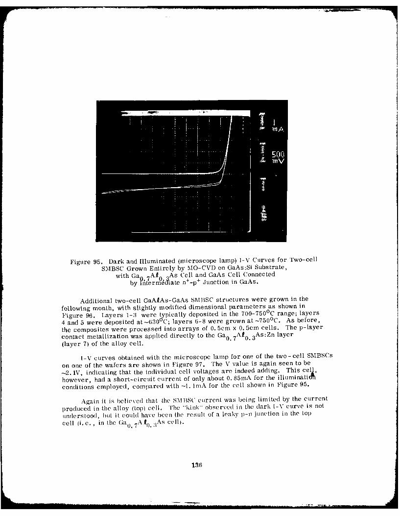
Figure 95. Dark and Illuminated (microscope lamp) I-V Curves for Two-cell
SMBSC Grown Entirely by MO-CVD on GaAs:Si Substrate,with Gaa 7 At I As Cell and GaAs Cell Connected
by Atermcdiate n+-p + Junction in GaAs.
Additional two-cell GaAfAs-GaAs SMBSC structures were grown in the
following month, with slightly modified dimensional parameters as shown in
Figure 96. Layers 1-3 were typically deposited in the 700-7500 C range; layers
4 and 5 were deposited at-630°C; layers 6-8 were grown at -750 0 C. As before,
the composites were processed into arrays of 0. 5cm x 0. 5cm cells. The p-layer
contact metallization was applied directly to the Ga 0.7At 0.3 As:Zn layer
(layer 7) of the alloy cell.
I-V curves obtained with the microscope lamp for one of the two-cell SMBSCs
on one of the wafers are shown in Figure 97. The V value is again seen to be
-2. 1V, indicating that the individual cell voltages are indeed adding. This cell,
however, had a short-circuit current of only about 0. 85mA for the ill uminatioMh
conditions employed, compared with -1. ImA for the cell shown in Figure 95.
Again it is believed that the SMBSC current was being limited by the current
produced in the alloy (top) cell. The "kink" observed in the dark I-V curve is not
understood, but it could have been the result of a leaky p-n junction in the top
cell (i.e., in the Ga 0 . 7A t 0 .3As cell).
136
L M
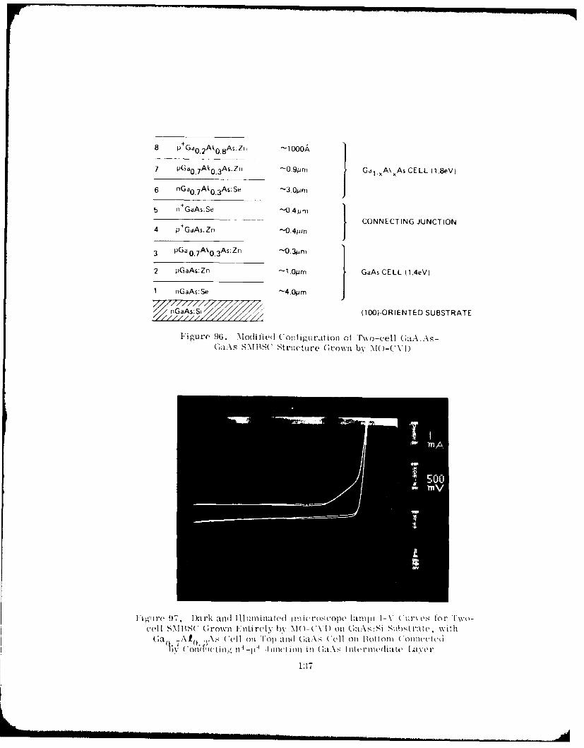
8 p'Ga0 2A 0 8 s.Zn ~ -000A
7 PGd0 7 Al 0 .3 As.Z1i -0.9pim Ga1 M A CELL (1.8eVj
6 flG 0 7 A 0 .3 As:Se -~3.0prn
5 nK+GdAs:Se -0.4pn 14 p Ga~. Zn--0.,umCONNECTING JUNCTION
3 pGa 0 .7 A 0 .3 As:Zn -0.3,um]
2 pGaAs:Zn "-l.Opm GaAs CELL (1.4eVI
1 nGaAs;Se -4.OpmJ
rGaAs:Si, 1100)-ORIENTED SUBSTRATE
Figure 96. )lOdi lied Conl tigUration ol I'wo-cell GaAAs-GaAs S.MRS3(' StruCtUre Grown bv OC .
irlire 97. * I)rk anIId li urnlimnaldIn ic roscope ia1npl 1-V (Uc sfor IFwo-cell S.M S( Grown F nireixy \i)N M()- (,I) Oil (;;sSuhstiiIrasIe , withi
Gia A(2 ('eli onl lois and G aAs (ell onl BottIoms Coisc ed7h ofnIdfuI (illi fll-p -insl ios isl I a.\s I slle Issledia tc ,aiver
1:17
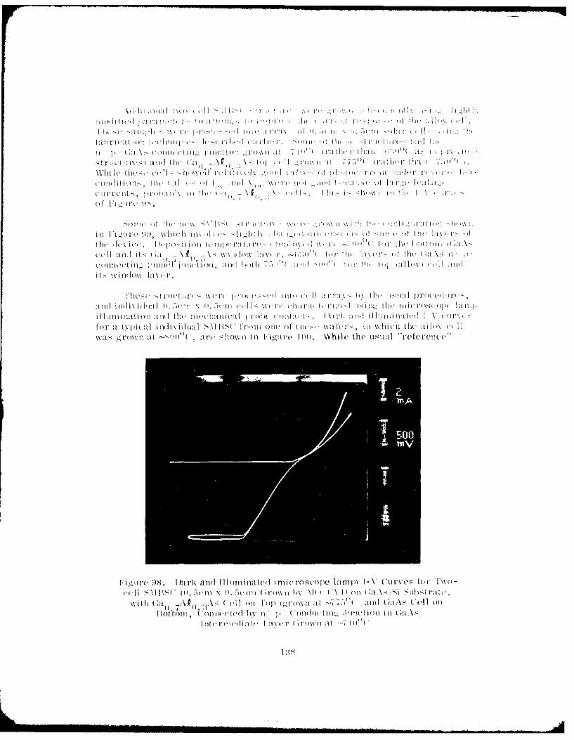
i i I i il It! -: It v I IA -II II I( it" It I'II II I
;i , -i ;aA s co (i (tIII I' i I:t1: & h 11: IlI r
s r Ii. i ( . n, n tVI iii I' (i , ., I1 t I I , I ti I I it ia M I I '1 h I I TI j i.
W ill 1( ih,-t ki--ts t~ I'.\ ., X iiiAX I I %- :1 h t I tin 1, I:I nV ri thu I r- '1:
CM I In i i I I it -I, Ii , ( II . In it s In -i I I I ; I Ih 'IS ii. r_ tu ti 'a~ ii t
ci l I [.; lii rotiiui : I hi iit) tI 1 (21 ; I I Ai - isi ,i h, M H III I 1Pi I~ It u I r1\i
- ,lt iw oft 'ilt) aI 'hIw %%I Vi 11 Ili,, ,~u~ the us i _ r nit ue 1
99re ilw I ll 'k In,: 11(0 "te1 i I IIIO(p lti- l Id- (II IIr I [hcr~ % t -
tlt (II 'l S cci .e I ti ' - I() it i nolt 11( 11 ( (;rnIiVirn_,I\l I Ill"() in I( ; I T, till 1)It lI ( ;:
uuH am sIWIan A d11o h h, (d ill (;~ i
colllc tll tlli e I. I on0 10 hi* I-," Il t, c l:1,
it.- ~ ~ ~ ~ w:ioSi av..
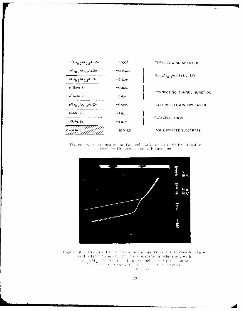
IP*Gd 0 2A 0 .As Zn ~ -10o0A TOP CE 1.1L WI(NDOW LAY ER
pG d0 3 A 0 .3 As. Zn 07p__________ (01 7A 0 3 As CE LL l.8eV)
nGa0 7 Al,0 .3As: Se -2.bpmJ
n4 GaAs;Se -04pm
_________ ___ I CONNECTING (TUNNEL) JUNCTIONIp4GaAs;Zn "- 4rni
pG a. 7 A 0 .3As:Zn ~ --O 5p m BOTTOM CELL WINDOW LAYER
pGaAs;Zn "'1 Opm
GaAs CELL I1.4eV)nGaAs:Se '-4.OpmJ
""~sSi10 MILS 11001 ()RIFNTED SUBSTRATE
12.t I'e 99. ((0t'! Hi i Iwm-ci l (;;t.\ \S-( ;tAsS\I S I (' toI i'i. 11( I iii it i '( j ills ' d i I )2, re 1'C I
Iilj( Ioo : I I i il l II I'( 'I m wi ro' is iii i 111 I V ( -i vcs fIor Iwo-
H'~~ol (;: !i- ) P l' ih
m l ,,)! , ;1' l 'o l
C~A
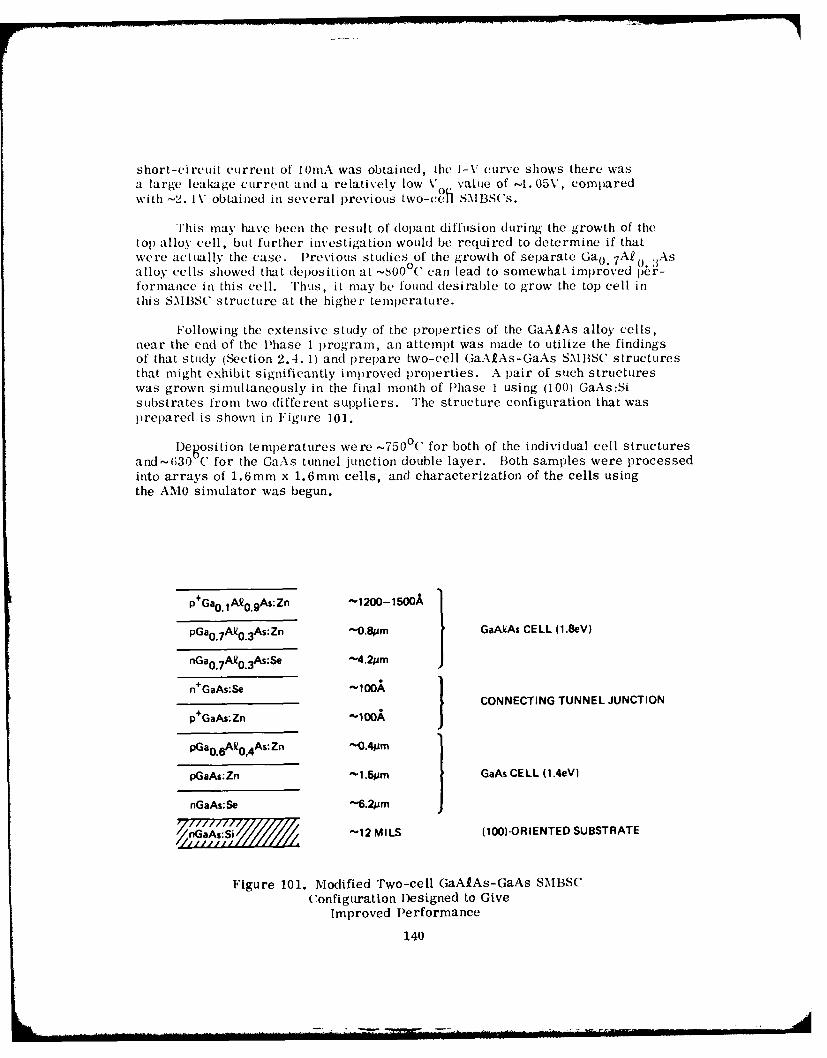
short-circuit current of l0mA was obtained, the I-V curve shows there wasa large leakage current and a relatively low V value of -1.05V, comparedwith -2. IV obtained in several previous two-Ch SMIIBSCs.
This may have been the result of dopant diffusion during the growth of thetop alloy cell, but further investigation would be required to determine if thatwere actually the case. Previous studies of the growth of separate Ga 0 . 7AM 0. 3Asalloy cells showed that deposition at -800°( can lead to somewhat improved per-formance in this cell. Thus, it may be found desirable to grow the top cell inthis SMBS" structure at the higher temperature.
Following the extensive study of the properties of the GaAfAs alloy cells,near the end of the Phase 1 program, an attempt was made to utilize the findingsof that study (Section 2.4. 1) and prepare two-cell GaAfAs-GaAs SMBSC structuresthat might exhibit significantly improved properties. A pair of such structureswas grown simultaneously in the final month of Phase 1 using (100) GaAs:Sisubstrates from two different suppliers. The structure configuration that wasprepared is shown in Figure 101.
l)e osition temperatures were -7500C for both of the individual cell structuresand-(30 C for the GaAs tunnel junction double layer. Both samples were processedinto arrays of 1.6mm x 1.6mm cells, and characterization of the cells usingthe AMO simulator was begun.
p+Ga 0 .1 A 0 .9As: Zn -1200-1500A
pGa0 .7 AV0. 3 As:Zn -0.8pm GaAkAs CELL (1.8eV)
nGa 0.7Al 0.3As:Se -4.2pm
n GaAs:Se -100ACONNECTING TUNNEL JUNCTION
p+GaAs:Zn "100A
pGa 0 .6Ak0,4 As:Zn "-0.4m
pGaAs:Zn "'1.5m GaAs CELL (1.4eV)
nGaAs:Se -6.2,um
,12 MILS (100)-ORIENTED SUBSTRATE
Figure 101. Modified Two-cell GaAiAs-GaAs SMBSCConfiguration Designed to Give
Improved Performance
140
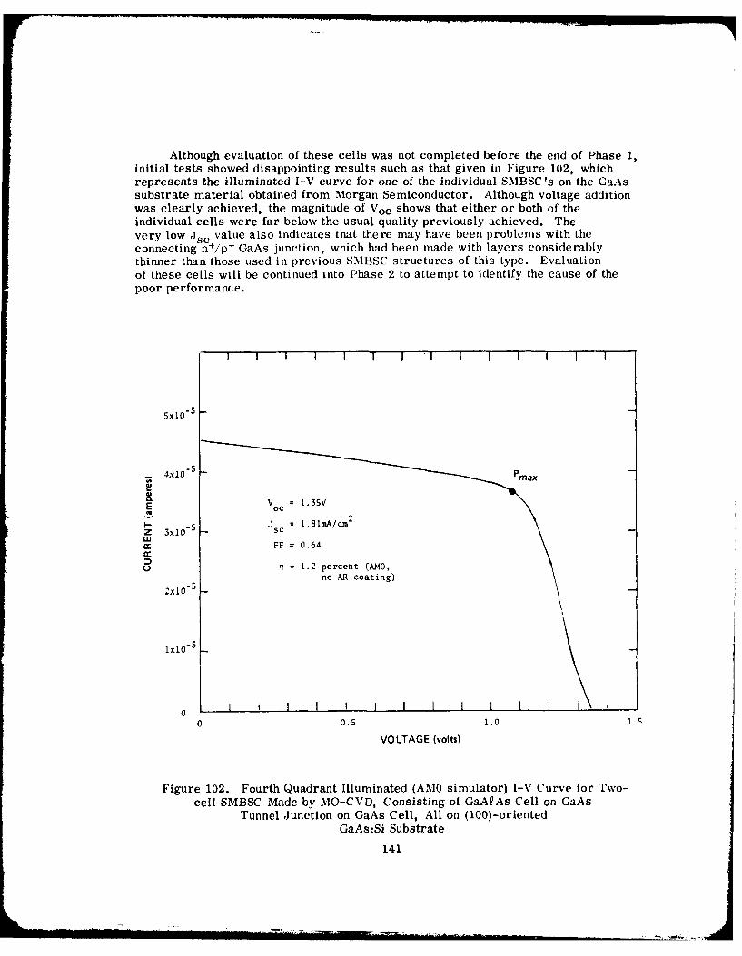
Although evaluation of these cells was not completed before the end of Phase 1,initial tests showed disappointing results such as that given in Figure 102, whichrepresents the illuminated I-V curve for one of the individual SMBSC 's on the GaAssubstrate material obtained from Morgan Semiconductor. Although voltage additionwas clearly achieved, the magnitude of Voc shows that either or both of theindividual cells were far below the usual quality previously achieved. Thevery low Jse value also indicates that there may have been problems with theconnecting n+/p+ GaAs junction, which had been made with layers considerablythinner than those used in previous SMBSC structures of this type. Evaluationof these cells will be continued into Phase 2 to attempt to identify the cause of thepoor performance.
I I I I I I I I I I I I
Sx10-5
4 x10-e3max
J = c 1.81mA/cm'
LUC FF = 0.64
U = 1.2 percent (AMO,no AR coating)
2x10⁻⁵
00 0.5 1.0 1.5
VOLTAGE (volts)
Figure 102. Fourth Quadrant Illuminated (AM0 simulator) I-V Curve for Two-cell SMBSC Made by MO-CVD, Consisting of GaAeAs Cell on GaAs
Tunnel Junction on GaAs Cell, All on (100)-orientedGaAs :Si Substrate
141
.. ~~ ~ .. ..++ ... ..... :- + .+.. • + ..
2.5 GaAkAs - G0 As - InGaAsP SMBSC TECHNOLOGY DEVELOPMENT
This task was to be carried out mainly at ERC Thousand Oaks, with the three-cell SMIBSC to be grown by IA'E techniques. GaAs xas to be used as the single-crystal substrate, and hi- as the window material for the l(aAsI) cell, which is anextension of the InGaAs cell to be developed as part of the two-cell SMIBSC assemblyin Task 3 (Section 2.3).
Although much of the work of this task was to be built upon the work of Task 3,certain aspects of the work were to begin at the start of the contract. The materialsand photovoltaic device properties of both the 2. 0eV G(LAIAs cell and the 1. 0eVlnGaAsf) cell made by 1I4E were to be studied in detail and characterized.
Near the start of the program the L PE growth of both n and p' layers ofGaAAs on p'GaAs substrates was to be carried out so that electrical conductionof n -p junctions in Ga.2 As could be investigated. Growtlh parameters requiredfor obtaining low-resistance conducting (tunneling) interfaces with good growthmorphology at the layer surfaces were to be established.
At the same time, the growth of appropriately doped p- and n-type layers ofGaAIAs in the proper composition for achieving a 2.0eV p/n LPE cell on an n+GaAssubstrate was to be undertaken, employing an ultrathin p-GaA2As surface layer.The photovoltaic properties of this 2.0eV cell structure were to be evaluated andthe layer growth conditions adjusted as required to obtain optimum cell properties.
When that goal was successfully achieved the GaA2As 2.0eV cell technologywas to be combined with existing conventional IAPE GaAs cell technolog-y. Startingwith the n GaAs single-crystal substrate, the (aAs heteroface cell structure(consisting of a p-type GaAIAs window layer on a p/n GaAs junction composite) wasto be grown on the substrate, followed by an n/p GaAfAs tunneling-junction doublelayer. On that would then be grown the GaAi As 2. oeV p/n cell structure describedabove, to complete a two-cell composite. The photovoltaic properties of thistwo-cell LPE-grown SMIBSC system were then to be fully evaluated (Task 6), andthe combined photovoltaic performance improved as much as possible by adjustilggrowth parameters and procedures.
Attention was then to be directed to development of the 1.0eV cell materialInGaAs1). Single-crystal substrates of p+In1 ) \were to be used for LI.E growth ofan inverted heteroface cell structure of n/p hnGaAsP, the photovoltaic properties ofwhich would be evaluated so that the growth parameters could be modified ifnecessary to produce satisfactory cell performance. When that was accomplishedthe expensive p+lnll substrate would be replaced by the plnII/n*GaAs epitaxialcomposite grown by LI)E on a single-crystal n+(aAs substrate in the early portionof the work of Task 3, and the same inverted n/p InGaAs P cell structure was to begrown on that composite. The photovoltaic properties of the 1.0eV cell would again beevaluated, and growth conditions further modified to optimize the cell performanceif necessary.
142
This teeluiology for the 10eV\ cell was then to be combined \\ith that alr'eadydeveloped (early in the program in this task) for preparing a (\co-cell structureinvolving the GaAs cell and the GaAfAs cell connected tlu'ough a tunneling intcrfa'e,to produce an integrated procedure for gro\ing a complete threc-cell SI SC by 1 iLKtechniques. Growth would be carried out on both sides of an 1 (aAs substrate toachieve the required struCturC.
As with the component StruCtures, the complete S.MBSC strl'cture \\as to bestudied and evaluated in detail; the photovoltaic properties of the complete three-cellassembly were to be determined and corpared with the corresponding properties ofthe individual component cells. Details of the overall fabrication process, includinggrowth sequence, individual layer compositions and i mpltrity concentrations, depo-sition parameters and cooling schedules, and contact materials and methods ofapplication were to )e carefully examined. Modifications indicated for achievingimproved ov .rail SMbSC performance would then be made to whatever extentpossible.
As in Task -, InGa 1' \vas to be considered as a possible alternative 2.0eV cellmaterial in this task, also, but grown by 1.1F'7 techiiques in this Case. The tfort, itpursued, would be at a lower level than the priimary activitV, as was to be the casefor the study of this material ;rovn by M()-C VI) in Task -1. It was intended thatsuch an investigation of L PE inGa 1) would be carried through the same stepwisesequence of investigations as that described above for GaAlAs with sufficientthoroughness that a substitution Could be mad( if difficulties of an unresolvablenature were to be encountered in developing the LPE Ga.\As 2.eV cell.
The possibility of using 1 BE techniques to form the nonrectifying connectingjunctions between ells of tile SMIBSC structures being investigated in this task wasexamined relatively early in the program . As indicated in the earlier discussion ofGaAs junctions (Section 2. 2.4), that method was successfully applied for that purposeas part of the activity of this task.
However, at the time the decision \ as made to change the program emphasislate in Phase 1 it was determined that the particular three-cell SMBSC that was thegoal of this task would not be further pursued in the Phase I prograin. It was alsoagreed that LPE growth techniques would not be further developed as part of theprimary program activity, but that iLE ncth,,ds would be used as backup or - incertain special cases - in conjunction with C\ D or MBE techniques if it appearedthat doing so would improve the chances of achieving the program goals.
The investigations carried out on this task during the Phase 1 program aresummarized in the following sections.
2. 5. 1 LPE Growth of GaAlAs on GaAs Substrates
Early in the program some preliminary tLE growth experiments were carriedout to prepare alloy layers with the approximate composition Ga 0 , 7 A10.:1As onp+GaAs single-crystal substrates. A compl,-te window-type solar cell structure,
such as that required for the 2.0eV cell () the three-cell S MBSC, was grown on an
14:t
n4GaAs substrate. This structure consisted ot a Ga0. IAIu.!jAs window layer on apGa 0 . 7 AI0. 3 As layer on an nGa0.7A 0.3'\s layer (Eg~1.9eV) on the substrate.
In addition, experimental growths were begun with p4GaAs single-crystalsubstrates for preparation of heavily doped p 4 Ga 0 . 7 A10. 3 As layers and thenn+Gao.7AI0.3As layers, in order to study the electrical properties of the resulting
n-~p - interface in GaAfAs, the interface expected to be a low-resistance tunnelingjunction when properly doped on the two sides. The first experiments gave layershaving reasonable surface morphology, but cross-contamination of the melts causedby incomplete wipe-off resulted in compensated and only lightly doped n-type GaAIAslayers, and thus only rectifying junctions were obtained.
Several possible methods for avoiding this difficulty were investigated,including chinges in the LPE boat design. A special boat design was developed, andconsiderable effort was devoted to finding an outside vendor capable of undertakingthe difficult fabrication tasks required by the design. A completed prototype wasfinally received from the selected fabricator in the ninth month of the program, atwhich time growth experiments were again undertaken in the GaAlAs-GaAs materialssystem.
Some minor modifications in the boat were found necessary, and when thesewere completed and the boat satisfactorily cleaned several attempts were made togrow GaAfAs layers of the properties required for use in a GaAlAs (1.7eV)-GaAstwo-cell SMBSC connected by a conducting or tunneling junction. Unfortunately,a leak in the H 2 purifier diaphragm occurred at about this time and made the firstgrowth experiments unsuccessful, but the experiments were resumed after repairof the purifier.
The LPE growth procedures with the new boat were improved to allow routineand reproducible growth of the desired layer thicknesses and alloy compositions.Several types of alloy cell structures were fabricated and characterized. Thestructures grown included those shown schematically in Figure 103.
Complete small-area cells were fabricated and characterized in structures ofboth the conventional grown-layer type and the Zn-diffused type, as shown at(a) and (b), respectively, in Figure 103. Some of the results are shown inFigures 104, 105, and 106, in which typical illuminated I-V and dark log I-V,sprectral photoresponse, and photoluminescence data, respectively, are given.
In general, these LPE cells were found to have good fill factors (typically0.7-0.8) but relatively dissappointing Voc and Ise values. On the basis of the deducedAI content, indicated by he bandgap cutoff of the photoresponse curve, the Voe valuesshould be about 1OOmV higher than those values typically observed. The Isc valuesshould be larger than those measured by a factor of 2 to 5. As is evident in thetypical photoresponse curve of Figure 105, there was very poor utilization of theshort-wavelength end of the incident illumination by these cells. It appears thatincreasing the A content of the window layer and optimizing the thickness of thewindow layer and the junction layer would improve this considerably.
144
INVERTED GROWNTHREE-LAYER THREE-LAYER JUNCTION AND DIFFUSED
GROWN JUNCTION DIFFUSED JUNCTION TUNNEL JUNCTION
LIGHT IN LIGHT INZn DIFFUSED
p+ A_.-0.9G _ _ P +A2.8-o. 9 G&As/ pAL 2 04 GAs TUNNEL
P At 0 "2 "0 "4GaAs p At0"2 4 GaAs n+A2t)..0.4GaAs 5JUNCTIONn A 0 2 4 GaAs n A%2 4 GA n A0 2 4 GaAs
-p AtV0 4Ga
&P* AIAOn.oGGaAs
ESUBSTRATE SUBSTRATE pGaAs SUBSTRATE
(REMOVED AFTER GROWTH)
LIGHT IN(a) (b) (c)
Figure 103. Three GaAfAs Large-bandgap Solar Cell Structures Grownby LPE Techniques, for Eventual Use in Two-cell and
Three-cell SMBSC's
Accordingly, some modifications were made in the parameters ol 'ectee-al 1,PE-grown window-type alloy cell structures that were prepared late in the Phase 1 program.The principal physical parameters of two of those structures are listed in Table 10.
Table 10. Principal Physical Parameters of LPEl GaAIAsHeteroface Solar Cell Structures*
Nominal Nominal Nominal Nominal Type of N1omnalSample A. Concentr. Window At Concentr. Junction Junction n La~er
No. (x) in Window Thickness (x) in Junction Depth Processed Thickness(Urn) (m) p m
LPE 1009 0.80 1.43" 0.30 1.0 Zn diffused 7.Ot
LPE 1011 0.80 0.57** 0.30 1.0 " 4.7t
S1.0tt As grawn
*Structures grown on (100) GaAs substrates at -100'C.
"Measured in SEM.
tMeasured in optical microscope.
ItFound to b. 0.71pm by measvrement.
145
1.4 x 10⁻⁵
1.2 x 10⁻⁵ -Prnax
1.0 x 10 5 -
&VOc , 1.0V0.8 x 10- - Isc , 1.3 x 10- 5 AFF = 0.76
z ? -0.4%
LU
0.2 x 10⁻⁵ -
0.2 0.4 0.8 0.8 1.0
VOLTAGE (volts)
n = 1.607
Jo 1.62 x10⁻¹⁴
amp/cm 2
10- 4
E10-5 (b)
10-
I
10-7 1 1 1 1 1 10 0.3 0.6 0.9 1.2 1.5 1.8
VOLTAGE (volts)
Figure 104. Typical a) Illuminated I-V Characteristic and b) Dark Log I-VCharacteristic of Zn-diffused-junction Window-type Ga 0 .6 1 AI 0 . 3 9 As
Solar Cell Grown by LPE (Type b, Figure 103)
146
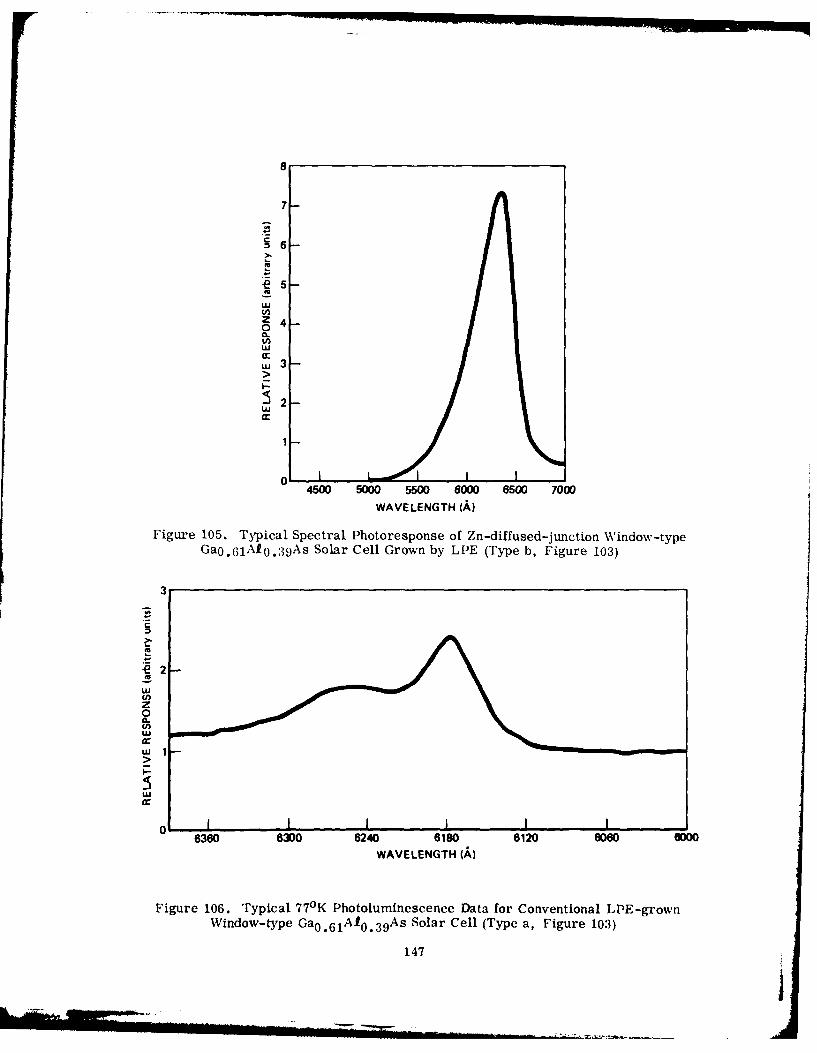
8
7-
6-
'U
e5
wZ 4-
w
0
a-
4500 5000 5500 6000 6500 7000
WAVE LENGTH (A)
Figure 105. Typiceal Spectral Photoresponse of Zn-diffused-junction Window-typeGa0.61A20.3 9 As Solar Cell Grown by LPE (Type b, Figure 103)
3
-J 2
00
6360 5300 6240 6180 6120 0060 6000WAVELENGTH (A)
Figure 106. Typical 77°K Photoluminescerce Data for Conventional LPE-grownWindow-type Ga0 . 6 1 A1 0 . 3 9 As Solar Cell (Type a, Figure 103)
147
3I.5d
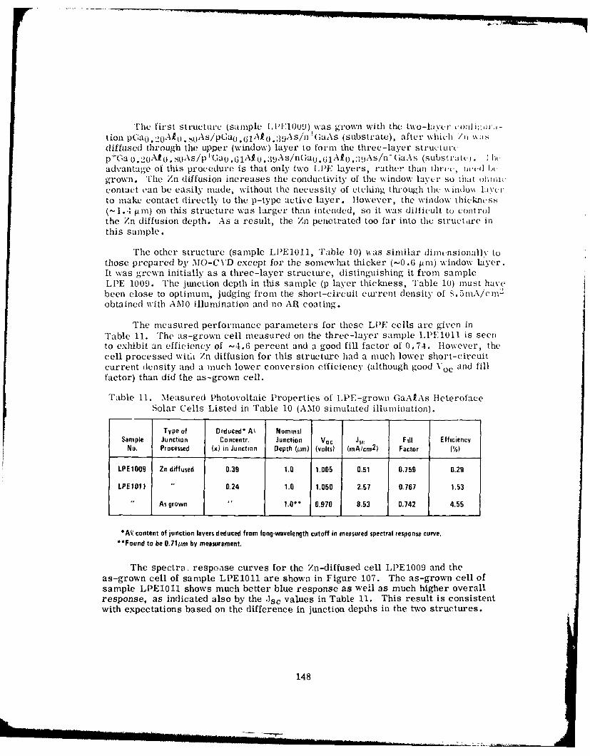
'The first structure (sample L1l1,009) was grown with the two-la ver -onfijgu ti,-tion pGa 0 .2 0 AI0.,o0 As/pGa 0 . 6 1 A 0.:0 9As/n (GaAs (substrate), after which /n \\JT
diffused through the upper (window) layer to form the three-layer struCttcp+GaO. 2 0AIo.,soAs/p+Ga0.G1Alo.:8gAs/tnGao.(lAfu.:yAs/n 5 (;aAs (subst-tMC). I hadvantage of this procedure is that only two LIPE layers, rather than thrt., Ittd Itgrown. The Zn diffusion increases the conductivity of the window layer so that ohnaicontact can be easily made, without the necessity of etching through the window Lsycrto make contact directly to the p-type active layer. However, the window thickncss(1.4 pim) on this structure was larger than intcnded, so it was dilficult to controlthe Zn diffusion depth. As a result, the Zn penetrated too far into the structure inthis sample.
The other structure (sample LlPE1011, Table 10) was similar dimensionally tothose prepared by MO-CVD except for the somewhat thicker (-0.6 pm) window layer.It was grewn initially as a three-layer structure, distinguishing it from sampleLPE 1009. The junction depth in thifs sample (p layer thickness, 'fable 10) must havebeen close to optimum, judging from the short-circuit current density of S.5mA\/cm2
obtained with AMO illumination and no AR coating.
The measured performance parameters for these LPE cells are given in
Table 11. The as-grown cell measured on the three-layer sample LPE1011 is seento exhibit an efficiency of -4.6 percent and a good fill factor of 0.74. However, thecell processed witli Zn diffusion for this structure had a much lower short-circuitcurrent density and a much lower conversion efficiency (although good Voc and fillfactor) than did the as-grown cell.
Table 11. Measured Photovoltaic Properties of LPE-grown GaAfAs tteteroface
Solar Cells Listed in Table 10 (AMO simulated illumination).
Type of Dpduced* Ak Nomin3lSample Junction Concentr. Junction Voc J i Fill Efficiency
No. Processed (x in Junction Depth (pim) (volts) (mA/cm2 ) Factor (%)
LPE1009 Zn diffused 0.39 1.0 1.005 0.51 0.759 0.29
LPE1011 " 0.24 1.0 1.050 2.57 0.767 1.53
As grown 1.0"* 0.970 8.53 0,742 4.55
*A content of junction layers deduced from long-wavelength cutoff in measured spectral response curve.
"Found to be 0.71prm by measurement.
The spectra. respoase curves for the Zn-diffused cell LPE1009 and theas-grown cell of sample LPE1011 are shown in Figure 107. The as-grown cell ofsample LPE1011 shows much better blue response as well as much higher overallresponse, as indicated also by the Jsc values in Table 11. This result is consistentwith expectations based on the difference in junction depths in the two structures.
148
; r .= .
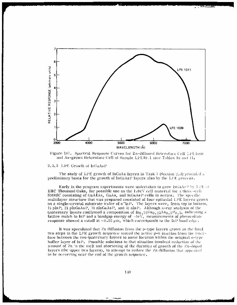
7
6~LPE 1011
n
>5
4-
z0
LUn
LU
1 1009
3000 4000 5000 6000 7000WAVELENGTH (A)
Figure 107. Spectral Response Curves for Zn-diffused Ileteroface Cell LI'I uo9and As-grown fleteroface Cell of Sample LPE10 I (see Tables 10 and 111
2. 5.2 LPE' Growth of InGaAsl1
The study of LPE growth of InGaAs layers in Task 3 (Section 2.3) provided :,preliminary basis for the growth of InGaAslP layers also by the LIE procss.
Early in the program experiments wvere Undertaken to grow hn(;a.\s 11v 1.'1- itERC Thousand Oaks, for possible use as the 1.0eV cell material for a three-cellSMIBSC consisting of GaAfAs, GaAs, and InGaAs 1 cells in series. The specificmultilayer structure that was prepared consisted of four epitaxial LIIE layers grownon a single-crystal substrate wafer of n+In 1. The layers were, from top to bottom,1) pln B, 2) plnGaAs 1, 3) nlnGaAs 1), and 4) nln 1). Although x-ray analysis of thequaternary layers confirmed a composition of In0 . 7 5 Ga 0 . 2 5 As0 . 5 1 0 . 5 , indicating alattice match to Ini, and a bandgap energy of -1eV, measurements of photovotaicresponse showed a cutoff at -0. 95 Vi, which corresponds to the In 1) band edgc.
It was speculated that ZIn diffusion from the p-type layers grown as the finaltwo steps in the LPE growth sequence moved tile active p-n junction front the iutcr-face between the two quaternary layers to some location within the original n-typcbuffer layer of InP. I'ossible solutions to that situation involved reduction of theamount of Zn 'n the melt and shortening of the duratic.a of growth of the tn-dopedlayers (the upper two layers), to attempt to reduce the Zn diffusion that appe'reto I)e occurring near the end of the growth sequence.
149
However, these possibilities Aere not pursued further with the lnGaAsPmaterials system. The question of Zn diffusion was addressed in the work withthe LPE growth of InGaAs layers in Task 3 (Section 2.3), but all LPE growthstudies in this materials system were finally curtailed when the programemphasis was changed later in Phase 1.
2.6 DEVELOPMENT OF AR COATING TECHNOLOGY
This task (Task 7) was intended to include the development of materials andprocesses to be used for fabricating the required AR coatings for the candidate cellassemblies considered for eventual use in Phase 2 of the program. It was originallyplanned that such developments would be completed before the end of the first phaseof the program, so that the performance of candidate SMBSC's could be establishedwith All coatings to provide the basis for selection or rejection of each for furtherdevelopment.
The plan originally developed to achieve that goal involved starting the work onthe materials and processes for AR coatings for the two-cell SMBSC configurationsin the seventh month of the program anm continuing it to the end of Phase 1, whilethat on the coatings for the three-cell composites was to begin in the tenth monthand continue through the remainder of Phase 1. In both cases, appropriate materialsand the processes for producing them in multilayer coatings that would result inreduction of reflection losses throughout the wide band of wavelengths for which theSMBISC is potentially effective as a power converter were to be identified. Thiswork was to be based in part on the modeling studies of Task I and in part on resultsof experimental measurements of reflection losses in the various multilayer struc-tures grown in Tasks 2-5, inclusive. The modeling studies were expected to identifyoptimum coating material parameters and number of layers in the AR coatings forvarious composite cell structures.
Experimental muttilayer coatings were also to be prepared in this task. Thestability of those experimental coatings under AN40 illumination was to be established,as was the effectiveness of each coating in improving cell performance. Based onsuch measurements, required changes in materiad compositions or in multilayerconfigurations and/or formation techniques would then be made to achieve thenecessary AR coating characteristics for the candidate SMBSC configurations.
After the program began it became clear that experimental deveLopment ofAR coatings should be delayed until other aspects of the experimental programhad advanced further. The multilayer AR coating design calculations that werecarried out as part of the Task 1 activities (see Section 2. 1. 1) were a prerequisiteto the development of practical AR coatings and coating procedures, but there wasno corresponding experimental preparation or development of the specific coatingsindicated by those calculations.
Development and application of suitable AR coatings will be involved in thePhase 2 program, as selected SMIBSC structures are further developed and requireoptimized performance conditions.
150
3. SUMMARY AND CONCLUSIONS
A 14-month (Phase 1) program of experimental investigation backed byanalytical modeling has been conducted to develop technologies required for fabricatingstacked multiple-ban'dgap solar cell assemblies having AMO 1-sun efficiencies of25 percent or greater at 25 0 C. Investigations were undertaken in the following fourSMIBSC materials systems, in accordance with the requirements of the contract:1) two-cell GaAs-Ge structure, made by MO-CVI) and conventional CV[) methods;2) two-cell GaAs-InGaAs structure, made by LPE techniques; 3) three-cellGaA2As-GaAs-GaAsSb structure, made by MO-CVD methods; and 4) three-cellGaA2As-GaAs-InGaAsP1 structure, made by LPE methods. After the program began,MBE deposition techniques were added to the investigations of structures 1, 3, and 4.With three months of Phase 1 remaining, a change in program emphasis was intro-duced by the Air Force to limit the investigations to GaA' As-GaAs and GaAs-Getwo-cell structures and the three-cell GaA2As-GaAs-Ge structure that might alsoresult. Principal emphasis was to be on the MO-CVI) technique, supplemented byMBE, LPE, or other deposition and/or processing techniques when appropriate forachieving the program goals.
The work carried out during the Phase 1 program is summarized below, by
task.
Task 1. SMBSC Modeling and Analysis
Previous work at Rockwell on the modeling of GaAs solar cell performance,both for normal one-sun illumination and for high-concentration (multiple-sun)illumination conditions, was used as the starting point for analytical studies of Gesolar cell performance, GaA2As heteroface cell performance, spectral photo-response of thin-window GaAs cells, and multilayer AR coating design.
The Ge cell modeling showed that the cell response for energies below the Gedirect bandgap (i.e., for X > 1.5 Am) drops very rapidly, even for a wafer-based
p+/p-/n cell structure and a substrate thickness of 300 pm, due to the limitedoptical absorption in the indirect-bandgap region (1.5 g A !c 1.8p m). Addition of aback-surface field (BSF) by formation of an n-n; junction at the rear of the structurehas little effect, for the same reason. However, the BSF was shown to be quiteadvantageous in very thin Ge cells (e.g., all-deposited structures a few Am thick)for energies above the direct bandgap - especially in the region 0.9 < X ! 1.5 Apm.
Modeling the performance of GaA As alloy heteroface cells having the struc-ture p+Gal-yA2yAs/pGalxA2xAs/nGa1_xACxAs (y- 0.8-0.9, x -0.2-0.3) andmatching the modeled response to the experimentally determined spectral responsesof such cells made by the LPE technique allowed estimates to be made of minoritycarrier diffusion lengths in the junction layers of these devices. This procedureindicated this parameter to be -0. 5 pm, in substantial agreement with empiricallydeduced values for the same parameter in the junction layer of similar device struc-tures grown by the MO-CVD process.
151
Similar matching of modeled and measured spectral photoresponses for thin-Si ndow Ga:\s cells made by the MBE technique was undertaken to obtain estimates
ol certain cell parameters and to provide some guidance in cell design. ltowever,sattisfactory match was not obtained unless window-layer thicknesses much larger thanthose known to be involved were assumed or much different rellectivity values thanthose used in the correction of the experimentally determine(] photoresponse datawere introduced. Based on these results it appears that specific reflectivity meas-urt'ne1ts must be made for each window-type cell evaluated if correct internalphotoresponse curves are to be obtained.
Analytical modeling techniques were also employed to develop an algorithm foruse in specifying the design parameters of n-layer AR coatings, where n 3, forapplication to SMBSC assemblies; these have spectral ranges broader than those ofany of the single cells involved. Some extension of the spectral range covered bytwo-laver AR coatings was shown to be possible by design changes, but it was foundthat far better broad-range coverage (e.g., 0.3-1.8 gm for two-cell or four-cellassemblies and 0.3-1.2 pin for three-cell assemblies) can be achieved with three-layer coatings employing MgF2 or CaF 2 for the top layer, Si0 2 for the middle layer,and Ta20 5 or TiO 2 for the bottom layer. Several specific multilayer coatings weredesigned, although there was no experimental development of these designs in Task 7because the status of the contract work in Phase 1 did not require it.
Task 2. GaAs-Ge SMBSC Technology Development
Investigation of the two-cell GaAs-Ge SMBSC structure received considerableemphasis. Initially, exclusively the MO-CVD process was used for growth of theGaAs heteroface cells and conventional CVI), utilizing the pyrolysis of GeH4 in H 2 ,for deposition of the Ge cell structures. Later in the program, however, the MBEtechnique was incorporated in the investigations for growth of both GaAs and Ge cells.
Attention was given to two possible SMBSC configurations. The preferred oneinvolved an epitaxial GaAs heteroface cell on an epitaxial conducting junction (eitheran n+ / p + junction in GaAs or an nGaAs/p+Ge heterojunction) on an epitaxial Ge cell,
all grown on a single-crystal n'Ge substrate wafer. The other involved a GaAsheteroface cell epitaxially grown on the front face of a single-crystal n+GaAs sub-strate wafer and an inverted n/p Ge cell grown epitaxially on a p+Ge epitaxial layerdeposited on the back face of the n+GaAs and forming the conducting intercell junc-tion. These configurations required reestablishing or developing satisfactorydeposition parameters for achieving high-efficiency GaAs heteroface cells, developingdeposition (or other) procedures for preparing good Ge cells, and developing methodsfor making conducting intercell junction structures. The combining of these com-ponents into functioning two-cell stacked assemblies was accomplished late in theprogram, but performance characteristics were not fully established.
The GaAs heteroface cells prepared on GaAs substrates by the MO-CVDprocess early in the program were decidedly inferior to those prepared in essentiallyidentical configurations in earlier studies at Rockwell. Contact definition andmetallization and series resistance problems were responsible for part of the situa-tion initially. The possibilities of continued processing difficulties and unidentifiedimpurities entering the cell structures from a reactant source tank were examinedsystematically to attempt to identify the cause, but no single obvious problem wasisolated.
152
Gradual improvement in MO-CVD GaAs cell performance continued throughoutthe program, however, to the point that cells with Voc = 0.97V, Jse 20mA/cm 2 ,fill factor 0. 8 and = 11. 5 percent (AMO, no AR coating) were being made by thefourth quarter. Use of a good AR coating would increase the AMO efficiency of suchcells to -16. 5 percent which, although not as high as the previous best performanceachieved at Rockwell in MO-CVD cells, was quite adequate for the purpose. Further,a very high degree of uniformity of MO-CVD cell performance over the area of sub-strates up to 2 cm x 4 cm was demonstrated by measurement of I-V characteristicsand spectral photoresponse of individual 0. 5 cm x 0. 5 cm cells processed in arrayson such substrates, illustrating one of the major strengths of the 'IO-CVD processfor large-area cell growth. It did not appear that variation in deposition temperaturewithin the preferred 700-7500 C range produced significant differences in overall cellperformance, but thinner GaA2As window layers (500-800A) and thinner p layers(-0. 75 Mm) in the active GaAs region did appear to give generally improved photo-voltaic response.
GaAs heteroface cells grown by MO-CVD on Ge substrates, however, con-sistently had higher leakage currents and generally poorer photovoltaic propertiesthan those prepared with nominally the same parameters on GaAs substrates. Thebest cells on Ge typically had parameters of Voc - 0. 96-0. 98V, Jsc - 16-17mA/cm 2 ,fill factor 0. 70-0. 75, and 7 - 8-9 percent (AMO, no AR coating). Uniformity ofcell performance over the area of a large substrate was also not as good as thattypically found for cells grown on GaAs substrates, indicating possible non-uninformities in the properties of the Ge substrate material used. Although deviceprocessing used early in the program may have been responsible for some of theseeffects other factors were probably dominant. Lower junction leakage and generallybetter cell performance were obtained when the Ge substrates were coated with-1000A of sputtered SiO 2 (except on the growth surface) to prevent interaction of thesubstrate and the MO-CVD reactant atmosphere. However, no attempt was made toevaluate the physical integrity of these coatings or to determine an optimum thicknessor deposition procedure.
Analysis by Auger electron spectroscopy of the interfacial region of epitaxialGaAs films grown by MO-CVD on (100)-oriented Ge substrates showed the width ofthe transition region to be dependent upon the specific experimental conditions usedduring initiation of the GaAs layer growth. A minimum "interface width" of -45,resulted when the TMG and the AsH3 were introduced simultaneously into the deposi-tion chamber to start GaAs growth. This was not the standard procedure, however.Clear evidence was found (primarily by x-ray topographic analysis) that GaAs-Gestructures grown with the standard predeposition procedure, involving exposure of thesubstrate to AsH3 for several minutes prior to introduction of the TMG to initiateGaAs growth, have a more defective interface region than do those prepared with amodified procedure in which the exposure to AsH 3 is of only a few seconds duration.However, less conclusive results were obtained for the photovoltaic performance ofresulting GaAs cells in the two cases, although the modified procedure does appearpreferable, especially in terms of the cell fill factor. Further investigation of thisproblem is required to provide more conclusive evidence.
Differences among MO-CVI) cells on GaAs and on Ge substrates were mostdistinct in the short-circuit current densities achieved, indicative of low photocurrent
153
collection efficiencies probably associated with low minority carrier diffusion lengthsin the defected GaAs layer adjoining the Ge. Modified cell design (layer dimensionsand doping impurity concentrations) and improved substrate quality are expected toresult in improved cell performance. No sharply defined preferred temperature wasobserved for GaAs cell growth on Ge, although the 700-7500 C range was again pre-ferred, with generally higher junction leakage currents resulting for higher tempera-ture growth and junction leakage plus excessive series resistance occurring forgrowth temperatures below - 6900 C.
Heteroface GaAs cells formed by the MBE process on GaAs substrates wereof generally good quality, even though relatively little program effort was devoted toexploiting the IBE technique for that purpose. The best cell performance wasrepresented by the following parameters: Voc = 0.94V, Jsc = 17.2mA/cm 2 , fill
factor = 0.84, and T1 ) 10. 1 percent (AMO, no AR coating); with a good AR coatingsuch a cell would have an AMO efficiency of over 14 percent. GaAs layers andnGaAs/pGaAs junction structures were grown by MBE on Ge substrates and were ofgenerally high quality, although the junction structures appeared also to involve apGaAs-nGe heterojunction formed unintentionally at the GaAs-Ge interface. Furtherinvestigation of such MBE structures was in progress at the end of the Phase 1 pro-gram and is expected to continue into Phase 2.
Formation of Ge solar cells was undertaken by conventional CVD techniques(GeH 4 pyrolysis in H2 ) and by MBE methods; limited experiments were also donewith spin-on oxide impurity sources to produce junction structures in bulk Ge wafersby thermal diffusion procedures. Since the most attractive configuration for the two-cell GaAs-Ge SMBSC is that in which the Ge cell, the connecting junction, and theGaAs cell are grown in sequence on a single-crystal Ge substrate, most programemphasis was on the formation of Ge cell structures on Ge substrates.
Although the GeH 4 pyrolysis reaction in H2 can be used in the temperaturerange -550-850 0 C, the best results were obtained at the higher temperatures(-8000 C), where the structural quality and surface morphology of the epitaxial filmsare best and the efficiency of incorporation of dopants (especially B from B 2 H6) ishighest. Unfortunately, the stability of the substrate - whether Ge or GaAs - isreduced at those temperatures, and some difficulties with out-diffusion of Sb (orother impurity) from Ge substrates and with As loss at the surface of GaAs substrates(with attendant liberation of Ga metal and subsequent entry into the growing Ge film)were encountered if lengthy deposition experiments were undertaken. The fact thatrelatively high Ge deposition rates (up to - 0.7 Wm/min) could be achieved at thehigher temperatures allowed relatively short growth times for most Ge layer thick-nesses. However, if prolonged depositions for very thick layers were to be neces-sary this could become a problem requiring further attention.
The Ge cell performance results improved considerably when the depositionexperiments were transferred from a GaAs MO-CVD reactor system to one that hadpreviously been used only for Si CVD. Ge cell structures were then made by growthof B-doped p-type layers on either undoped n-type layers or directly on doped n-typeGe substrate wafers. The best cells had the following characteristics:Voc 190-200mV, Jsc = 31-33mA/cm 2 , fill factor = 0.65, and 7 = -3 percent (AMO,no AR coating); with a good AR coating to reduce reflection losses an AMO efficiency
154
ol -4 percent would result for such a cell. It is clear that intentionally doped n-typelayers, rather than the nominally undoped n-type layers used in all of the cell struc-tures investigated, must be employed to improve the photovoltaic properties of theCVI) Ge cells. Also, relatively minor changes in cell design parameters - especiallylayer thicknesses and doping concentrations - should result in significant improve-ments in cell performance. Modifications in the Ge cell contacting procedures(especially the contact alloying schedules) are required to allow maximum device per-formance to be achieved for any cell design. These improvements should be pursuedin the Phase 2 investigations.
Ge cell structures were also made by MBE techniques late in the Phase 1 pro-gram. A layer of As of appropriate thickness was deposited on p-type (100) Ge inthe MBE apparatus and subsequently diffused at elevated temperature to produce adiffused n-p junction. The resulting cells, although not as good as those formed byCVD, were adequate for use in preparing two-cell stacked GaAs-Ge structures byMBE techniques.
Connecting intercell junction structures for GaAs-Ge SMBSC's were made inGaAs by both MO-CVD and MBE as well as by a combination of the two depositiontechniques. Although a few n+GaAs/p+Ge heterojunction structures were grown byMO-CVD early in the program, attention shifted at an early date ton+GaAs/p+GaAs and p4GaAs/n*GaAs structures grown on GaAs and Ge substrates.Deposition temperatures ranged from 630 to 7500C, with generally better resultsbeing obtained at the lower temperatures (g6500 C). Good tunnel junction character-istics were obtained in p /n+ structures (each region -0.6 ,m thick) grown at 6500 Con GaAs substrates, with peak-to-valley ratios of 4:1 and peak current densities upto -100 mA/cm 2 . Good tunneling characteristics were also obtained in n /p - struc-tures of similar dimensions grown at -630oC, with an almost linear I-V character-istic indicating very high conductivity - more than adequate for use as an intercellconnection under 1-sun AMO conditions.
Despite the fact that preliminary annealing tests of some of the tunnel diodestructures indicated that the tunneling characteristics might not survive subsequentelevated temperature processing required for growth of the top cell in a stacked eel'assembly, the n+/p+ GaAs structures grown at 6300C were used in producing thefirst two-cell GaA9 As-GaAs SMBSC's. (Similar SMBSC structures employingn+GaAC As/p GaA2 As as the connecting junctions were also prepared, but only thestructures with the connecting junction in the GaAs exhibited tunneling properties.)The extent to which the MO-CVD tunnel diode structures, which involve Zn as thep-type dopant and Se as the n-type dopant, would consistently survive subsequentelevated-temperature processing remained an unanswered question to the end of thePhase 1 program and will require further investigation in Phase 2.
However, the formation of p'GaAs layers by MBE techniques with Be, a slow-diflusing impurity in GaAs, as the added acceptor provided a possible alternativesolution to this problem. A hybrid n+/pt tunnel junction structure, consisting ofn 4 GaAs:Se formed by MO-CVD at -630oC on p+GaAs:Be formed by MBE on a GaAs:Crsubstrate, exhibited usable tunneling properties, although not as good as those of theall-CVD structure grown at 6300C. Tunnel junction structures ofn+GaAs:Sn/p++GaAs:Be, with thick (-l m) layers deposited entirely by MBE tech-niques on p GaAs single-crystal substrates at-5400 C, exhibited ohmic behavior.
155
\\hen thinner (-500A) junction layers were use(d similar low-resistance ohmicconduction resulted. Thermal cycling tests of both structures showed that therewere no adverse eflects on the high conductance ol either one following exposure toa temperature-tinme cycle typical of that involved in Ll1F growth of a window-t ,p)eGaAs solar cell structure. It thus appears that a satislactory connecting junctionthat will survive subsequent high-temperature processing can be made in GaAs bythe .MBF technique.
Experimental two-cell (;aAs-(Ge stacked assemblies were made entirely byMBE techniques and by combined NlO-CVI) and .1BE near the end of the Phase 1program, but no such assemblies were completed using CVD techniques exclusively.The all-MBE structure appeared to contain a complicated double heterojunctionrather than the intended two-cell and tunnel-junction structure. The hybrid struc-ture involved a heteroface GaAs cell grown by MO-CND at 7500C on annGaAs:Se 'p GaAs:Zn tunnel junction grown by MO-CVb at 630 0 C on a Ge cell struc-ture made by MBE techniques. Processing of this stacked assembly was not com-pleted before the end of Phase 1, however. Additional S3MBSC structures involvingGaAs and Ge cells prepared by various combinations of CVD and MIBE techniques areexpected to be prepared and evaluated in Phase 2. In particular, structures involvingMIBE-grown tunnel junctions should be exploited because of the apparent temperaturestability of the Be-doped p-type GaAs prepared by MBE.
Task 3. GaAs-InGaAs S*IBSC Technology Development
Investigations of the two-cell GaAs-InGaAs SMBSC system to be made by LPEgrowth methods on n+GaAs substrates involved principally the experimental growthof InP and InGaAs layers on lnP and GaAs single-crystal substrates and an evaluationof the AlGaAsSb materials system as an alternative to InGaAs for the low-bandgapcell of this SMBSC structure.
Experimental LlPE growth of p+InP layers (to serve as the lattice-matchedwindow material for the low-bandgap InGaAs cell) on n+GaAs substrates was onlypartially successful. Growth from both In and Sn solvents was studied, with theformer producing acceptable growth on (I11B)GaAs in a narrow temperature rangearound 520 0 C and the latter resulting in rough but marginally acceptable layers on(100)GaAs at higher temperatures (600-8000 C) provided that large vertical tempera-ture gradients were maintained across the liquid-solid interface to maintain thesubstrates below the temperatures normally indiced by the process, thus minimizingetch-back. However, high densities of In inclusions persisted at the growth inter-face, rendering the structures impractical for use in stacked cell configurations.Therefore, to circumvent such difficulties, InP layers were grown separately onGaAs substrates by the MO-CVD process for use in the subsequent LPE growthexperiments with lnGaAs.
LPE growth experiments were undertaken with the lattice-matched (to lnP)ternary composition Ino.52GaO.48As. Several p-n junction structures were grown,initially on single-crystal (l1B) InP substrates. Despite some problems in makingohmic contacts, these structures were characterized and found to have low currentcollection efficiency as well as questionable stability of location of the junction, dueto probable movement of Zn (the p-type dopant) during the LPE growth process.
156
There was also some evidence that an i il-InGaAs heterojunction had resulted,producing defect-assisted tu unelinrg cu r'elnts rather that) simple p-n junctioncharacteristics.
Growth ot thicker undoped In(aAs layers at relatively low temperatures(.630°(0) on polished (1 l lt)-oriented pt lPl substrates, with slight substrate etch-back prior to growth, resulted in n-type material ol approximate compositionIn0 . 5 3 (.;aO 4 7 As (bandgap energy -0. 7 eV) in which a junction was evidently formedby Zn1 out-diILfusion Irom the substrate. Solar cells fabricated from this materialexhibited VoC values <0. IV and .Sc valueCs 01 -16mA/cm 2 (AMI, no Ali coating),with the low photovoltages attributed to large Jo values and poor diode factors.There was some indication that in additional barrier - perhaps a heterojunction atthe l nGaAs-hnil interface - had been formed during the growth process.
Some preliminary experiments were then undertaken with growth of InGaAs onthe MO-CVD nlI/GaAs composite samples previously prepared, but discontinuouslayers with poor melt wipeoff were obtained, probably due to the extreme cautionexercised in attempting to avoid loss of the relatively thin In1) layers by meltback asgrowth was being initiated. The work was not pursued further, however, becauseof the change in technical emphasis introduced late in the program.
When the problems were first encountered in the lnll/InGaAs system early inthe program some attention was diverted to A GaAsSb as a possible alternativesmall-bandgap cell material. Window-type cell structures were grown onl n-typesingle-crystal GaSb substrates by LPE with the configurationpGaO. 7A 0. 3AsSb/pGaSb(undoped)/nGaSb(substrate), but poor photovoltaic properties(especially fill factor and short-wavelength response) were obtained. Modifiedstructures, with improved contacts to reduce series resistance and thinner pGaSblayers to improve short-wavelength response, were then prepared with the configura-tion p'Ga.7Ae 0. 3 AsSb/pGa0 .9A 0. 1Sb/nGaSb (substrate). Addition of A to theGaSb p layer reduced the layer growth rate, so that shorter deposition times (-1 minat -520oC) allowed growth of p layers that were 2-3 lm thick.
These changes allowed attainment of cells with the parameters Voc - 0. 240V,Jsc = 29mA/cm 2 , fill factor = 0. 51, and ?1 -3. 5 percent (AM1, no AR coating).Junction leakage and series resistance remained as problems, but the results weresufficiently encouraging to prompt a brief investigation of various contact materialsfor both p-type and n-type GaSb to attempt to reduce series resistances losses. PureAu contacts were found best for both conductivity types. Several additional cellstructures, including some with higher A? composition (,-0. 7) in the window layer,were subsequently prepared, but the investigations were not carried further becauseof the change in program emphasis invoked at that time.
Task 4. GaAleAs-GaAs-GaAsSb SMBSC Technology Development
Investigations of the several technologies required for the three-cellGaAAs-GaAs-GaAsSb tandem structure were given major emphasis. It was origi-nally expected that exclusively MO-CVI) techniques would be used to make this struc-ture, but MBE methods were introduced to supplement the MO-CVD process part waythrough the program. Also, near the end of Phase 1 the program emphasis wasshifted to the GaAe As-GaAs-Ge materials combination, at which time no lurther effortwas directed to GaAsSb as the small-bandgap material.
157
The technologies requiring most of the development attention were the growthand labrication of satisfactory (aAe As cells with 1.8-2.0 eV bandgaps, the prepara-tion ol high-conductance connecting junctions in GaAVAs and/or in GaAs (the latteralready described), the growth and tabrication of GaAs 0 . 5 Sb0 .5 1. 0 eV cells byl)-CVI), and the combining of the components into a stacked cell assembly. Experi-
mental studies were conducted in all of these areas except the preparation of GaAsSbcells by .MO-CVI); this materials system was investigated briefly using LPE tech-niques, as noted above, but MO-CVI) studies had not been undertaken prior to thetime at which the program emphasis was changed.
The experiments with GaA As large-bandgap cell structures were essentiallyall (]one with nGaAs:Si or GaAs:Te substrates. Cell configurations were typicallyp Gal_ vAs '(;alxAiXAs/nGal_xAt\xAs (y 0.8, x 0.2-0.4), in some cases witha thin ( aAs:Zn cap layer on top of the window layer to facilitate contacting thejunction layer of the cell. Deposition temperatures ranged from 700 to 800 0 C, with7500 C the most commonly used. Most completed cells were 0. 5 cm x 0.5 cm,although small individual mesa cells in several sizes were also fabricated at times.(;ood I-V characteristics (dark and illuminated) were obtained with these devicesalmost from the start. Cell response appeared to improve generally with increasingdeposition temperature, and compositions with x - 0.24 in the active regions gavebetter performance than those with x 0.3 or 0.4 in these early devices.
It became clear, from analysis of the performance of the first two-cellGaAeAs-GaAs SMBSC's, that the alloy cells were probably the main limiting factorin performance of the stacked structures. Spectral response measurements onseparate alloy cells with various layer dimensions and design parameters showedthat reduced short-wavelength responses were responsible for the relatively smallJsc values typically obtained with these cells, although the degree of uniformity ofresponse among an array of 15-20 cells formed on a single large GaAs substratewas extremely high. It appeared that poor current collection efficiency (i.e., smallminority-carrier diffusion length) in the pGaAeAs active layers was most likelyresponsible for the reduced high-energy responses. The best parameters observedwith alloy cells grown at -750oC on an n4GaAs substrate and having the nominal con-figuration pGa 0 2 AV%0 8 As(I000,)/pGa 0 7 6 A20 2 4 As(0. 6 Mm),'nGa 0 . 7 6 AC 0. 2 4 As(2.4 Am)were Voc 0.96V, Jsc = 12.OmA/cm 2 , f ill factor - 0.63, and il - 5.4 percent (AMO,no AR coating).
Late in the program several groups of alloy cells with window-layer thicknessesfrom 0. 08 to 0.15 pm, and Zn-doped p-layer Ae compositions of x - 0. 1S-0.35 andthicknesses ranging from 0.3 to 1. 5 pm were grown at -750 0 C. It was found thatVoe increased as the A content of the junction-forming layers increased, especiallyfor x >0.2, but the Voc values were appreciably less than the theoretically expectedvalues for all but very low (x <0. 10) At' compositions. The highest Voc valueobserved was -1. IV for cells in which x 0.35. The 'sc values were shown todepend upon both At' content and thickness of the window laver as well as the Junctionlaver. \cti e layer compositions with x -0.3 seemed superior, and junction depthsless than -0. 7 p nm were clearly preferred, with thicker p layers causing reductions:n isc. This indicated that minority-carrier dit lusion lengths were probably <0. 5 p min the (;aAiAs p layers made by MO-('VI). Spectral response measurements showedthat window laver compositions with y 0.9 allowed better blue response and higher,,( Isalu(es than those with v 0.8, and window layer thicknesscs <S00A M.vre pre-ferred. Most cells had .sc values less than 6 mA /cm 2 for AMO illumination, no
158
ill -.
matter what compositions or dimensions were involved; till factors ranged Iron 0.60to 0.76 and efficiencies were --4 percent (no Ai coating).
A few alloy cells were processed with Zn dilfused into the window layer toincrease its conductivity and produce a tront-surface field as a possible means olimproving cell performance. Although this procedure (lid appear to increase the*'se values or some MO-CV) cells, it had the opposite ellect for other MO-CVI)cells and for the LIIE Ga.\V As cells on which it was used, so it was not turtherpurSied. As of the end of the Phase 1 program the performance of the GaAtAs cellsstill required considerable improvement, so continued emphasis in this area isanticipated in Phase 2.
Several attempts were made to achieve tunneling properties in GaAk'As junctionstructures grown by MO-CVD, beginning early in the program, lor the purpose olproviding the connecting junction between GaALAs cells and GaAs cells in stackedassemblies. Both n' /p and p /n' junction structures w'th GalvA As composi-tions of y 0.08 to y 0.37 were grown at temperatures of 700 and 7500 C, but atbest only weak tunneling was observed. Although the emphasis in the remainder ofPhase 1 was on tunnel junction structures in GaAs, it is expected that further effortwill be devoted to achieving tunneling structures in the alloy in the Phase 2 programsince that configuration is preferred in terms of overall performance o the stackedassemblies.
Two-cell GaAI As-GaAs SMBSC's were fabricated and tested approximatelymidway through the program, as soon as evidence of tunneling in n'/p" structures inGaAs had been observed. Although such structures were made with the connectingn /p junction structure both in GaAs and in GaAk As, only the former exhibitedadequate tunneling properties. The successful configuration wasGaA 'As cell/GaAs n*-p' junction/GaAs cell, grown by MO-CVI) on an nGaAs:Sisubstrate. Best results were obtained with a structure in which the alloy cell con-figuration wasp+ Gao. 2 A O. 8 As:Zn(1000A)/pGa 0 . 7 Ae 0. 3 As:Zn(0. 75 .im)/nGa0 . 7 Ak o. 3 As:Se(2. 5 tmn).The tunneling junction was n-GaAs:Se(0.4 gm)/p' GaAs:Zn(0. 4 um) and the GaAs cellwas pGa0. 7 Ac' .3 As:Zn(0. 5 pim)/pGaAs:Zn(1. 0 j.m)/nGaAs:Se(4. 0 Wm). Growthtemperatures were 750, 630, and 700 0 C, respectively, for the three componentregions.
Under tungsten lamp illumination this SMBSC exhibited a Voc of -2. 1V and a•sc of -4. 5mA/cm 2 . This represents the first successful achievement of a stackedcell grown completely by a vapor-phase process and exhibiting voltage addition. TheVoc value is believed to be the highest achieved up to that time for a stacked cellgrown by any process. It appeared that the Ga 0 . 7M0.3As cell in this structure wasprobably the limiting component in the performance of the stacked assembly, pre-venting higher photocurrents from being collected.
Because of some evidence that better alloy cell performance was obtained forhigher growth temperatures, some GaAs As-GaAs stacked structures were grown inwhich the alloy cell was deposited at 775 and 800 0 C, but increased leakage currentsand lower Voc values were obtained in each case. Further investigation is requiredto determine if these effects may have been caused by dopant diffusion in the lowerlayers of the structure (luring growth of the alloy cell at the higher temperatures.At the end of Phase I several additional two-cell stacked structures were grown with
159
greatlV reduced thicknesses in the tunnel junction layecrs ( 1 0GA each) and the alloycell deposited at 750( to attempt to inprove the properties of the resulting SMIS('.initial evalaMtion 0f Some 01 the cells, although not com1plete, indicated that theintended improvements had not been achieved. Thus, work with the (a:\ As-(Ga>\stwo-cell tani1dem structure must be continued into the Phase 2 program in order torealize the oerall pierformance expected of this materials combination.
Task 5. GaA, As-(;aAs-ln(;aAsl' S.IIBSC Technology Development
The study 01 the three-cell GaA, As-GaAs-InGaAs P) SM BS( assembly to bemade by 1.1PV methods using both surfaces of n '(aAs single-crystal substratesinvolved two main areas of investigation - LPlF growth of 2.0 eV (aA As cell strLIc-tures on GaAs surfaces and LIIE growth of 1. 0 eV [nGaAs 1' layers. Fxisting well-established methods for I.lBE growth of GaAs cells provided the third major celltechnology. The GaAs (or GaA, As) tunnel junctions and In 1) GaAs tunneling hetero-junctions develolped in other tasks and employing either PE' or MI,. techniques wereexpected to provide the needed cell interconnections.
Window-type alloy cell structures were grown by LPl'E on na_-\s substratesearly in the program, with the configurationp* Gao. 1 A, 0.9As / pGa 0
. 7 A
L 0 .3 As/nGa0
. 7A
,' 0 . 3As. Some experimental n' p" alloystructures were also grown, but incomplete wipeoll in the L1E boat resulted in cross-contamination of the melts and unsatisfactory structures. A special LIIF boat wasthen designed, and fabrication was completed bv an outside vendor several monthslater. Modified IAF growth procedures were developed for use with the new boat,and several ty'pes of alloy cell structures were prepared.
Complete small-area window-type cells were fabricated both by conventionalprocessing and by processing that involved Zn diffusion into the window layer.\Window-laver A contents were in the range y - 0.8-0. 9 and junction layer Ae con-tents x 0.2-0.4. The cells generally had good fill factors (typically 0.7-0.8) butrelatively low Voc and Ise values. Spectral response curves showed poor utilizationof the short-wavelength illumination, indicating needed changes in window layerthickness and junction layer thickness and AP content.
Some additional alloy cells were prepared near the end of Phase 1, includingseveral in which only a p-type active layer and a p-type window layer were depositedir succession by LPE on an n'GaAs substrate, followed by Zn diffusion through thewindow laver and the p layer to produce the active p-n junction, just inside the sub-strate. However, in the abbreviated investigation it was found difficult to controlthe diffused junction depth. The cells grown and processed by conventional procedureswere somewhat better; Isc values up to 8.5mA/cm 2 and efficiencies up to 4.6 per-cent (AMO, no AR coating) were obtained. Open-circuit voltages ( -l.0V)and fill factors(-0. 75) were about the same for both types of cell.
Only limited investigation of the LPE growth of InGaAsP for the 1.0 eV bandgapcell was undertaken. Multilayer structures of the configurationplnlI 'plnGaAsl)/nln(;aAsl)/nlnl ) were grown on n+lnP substrates. Analysis showedthe quaternary layers had the composition In 0 . 7 5 Ga 0 . 2 5 As 0 . 5'0. 5, indicating abandgap of ,,eV and a lattice match to In P, but photoresponse measurements showed
160
cutoff at the lnl band edge. This was believed caused by Zn dopant diffusion fromthe two upper layers into the nlnl buffer layer, shifting the active junction to thatlocation. Although the problems of Zn diffusion in IAIE growth in the InGaAs systemwere examined in the Task 3 studies, the investigation of the quaternary was notcarried further in Phase 1.
Task 6. Characterization ol Materials and Photovoltaic Devices
Descriptions of the activities of this task are included in the other taskdiscussions.
Task 7. Development of AR Coating Technology
There was no experimental development of specific AR coatings for the variousSMBSC's investigated during Phase 1. Although multilayer AR coating designs weredeveloped in the Task 1 modeling and analysis studies, the preparation of appropriatecoatings was postponed until Phase 2 of the program.
161
4. REFERENCES
1. J. J. Loferski, J. Appl. Phys. 27,777 (1956).
2. M. Wolf, Energy Conversion 11,63 (1971).
3. K. 1) Jackson, Transactions of the Conference on the Use of Solar Energy,lucs n, AZ, october 31-November 1, 1955, p. 122: also U.S. PatentNo. 2,949,4!) , issued August 16, 1960.
.1. J. J. Loferski, Proc. of the 12th IEEE Photovoltaic Specialists Conference,Baton Rouge, LA. 1976, p. 957.
5. N. S. Alvi, C. E. Backus, and F. W. Masden, Proc. of the 12th IEEEPhotovoltaic Specialists Conference, Baton Rouge, LA, 1976, p. 948.
63. W. Shockley and H. Queisser, J. Appl. Phys. 32,510 (1961); also M. WolfRef 2.
7. R. Sahai, private communication.
8. R. D. Dupuis, P. D. Dapkus, R. D. Yingling, and L. A. Moudy, Appl. Phys.Lett. 31, 201 (1977).
9. C. 0. Bozler, J. C. C. Fan, and R. W. McClelland, in GaAs and RelatedCompounds (Inst. of Fhysics, London, 1979), p. 40.
10. R. Sankaran, R. L. Moon, and G. A. Antypas, J. Cryst. Growth 33, 271 (1976).
11. Air Force Contract No. F33615-C-77-1005.
12. T. Sukegawa, T. Hiraguchi, A. Tanaka, and M. Hagino, Appl. Phys.Lett. 32, 376 (1978).
13. M. B. Panish, J. Appl. Phys. 44, 2667 (1973).
162
*U,S,Government Printing Office: 1981 - 757-002/383