Embed Size (px)
Citation preview

AD-A124 064 AN INVESTIGATION OF ORDERING TEARING AND LATENCY I/tALGORITHMS FOR THE'TIME-.. (U) ILLINOIS UNIV AT URBANACOORD INATED SC IENCE LAB P YANG AUG 80 R-891
UNCLASSIFIED NO014-79-C0424 F/G 9/5 NLEIIIIIIIIIIIEIIIIIIIIIIIIuMhEOOEEhNIEIIIIIIIIIIIIIMIIIIIIIIIIIIIIIIIIIIIIIIIIIIIIIEEEIIIIEEIIIIE

Hill; 1* .I28 125
milla
1.5~l. 1111.
M ICROCOO RlRhLUtL)N I', I T HARI

REPORT R-891 AU ST, 1980 UILU-ENG 80-2223
I?,1CORDINA TED SCIENCE LABORATORY
U AN INVESTIGATION OF ORDERING,TEARING, AND LATENCY ALGORITHMSFOR THE TIME-DOMAIN SIMULATIONOF LARGE CIRCUITS
PIG YANG
IIIII
A ," ' PUBLIC *WAh. CHSTRINUTION UNLIMITED.
ECTE3
i ~~~JA 3 1983E
"I UNIVERSITY OF ILLINOIS - URBANA, ILLINOIS1 83 01 31 102
|rl~a I" I ii iI~i - -

UNCLASSIFIEDSECURITY CLASSIFICATION OF THIS PAGE (When Doe. Entor*d)
REPORT DOCUMENTATION PAGE READ INSTRUCTIONSBEFORE COMPLETING FORMI. REPORT NUMBER 2. GOVT ACCESSION NO. 3. RECiPIENT'S CATALOG NUMBER
4. TITLE (and Sublils) S. TYPE OF REPORT & PERIOD COVERED
AN INVESTIGATION OF ORDERING, TEARING, AND LATENCYALGORITHMS FOR THE TIME-DOMAIN SIMULATION OF LARGE Technical ReportCIRCUITS 6. PERFORMING ORG. REPORT NUMBER
R-880; UILU-ENG 80-22127. AUTHOR(o) 6. CONTRACT OR GRANT NUMBER()
Ping Yang N00014-79-C-0424
4 9. PERFORMING ORGANIZATION NAME AND ADDRESS 10. PROGRAM ELEMENT PROJECT, TASKCoordinated Science Laboratory AREA & WORK UNIT NUMBERS
University of Illinois at Urbana-ChampaignUrbana, Illinois 61801
1I. CONTROLLING OFFICE NAME ANO ADDRESS 12. REPORT DATE
August 1980Joint Services Electronics Program 13. NUMBER oF PAGES
17614. MONITORING AGENCY NAME & ADDRESS(II dif erent from Concroiling Office) IS. SECURITY CLASS. ro( this report)
UNCLASSIFIED
IS&. OECL ASSIIrlCATION/ DOWNGRAOINGSCH E DU LE
16. OISTRISUTION STATEMENT (of che aReport)
Approved for public release; distribution unlimited
17. DISTRIBUTION STATEMENT (ot the *bstract entered in 81'ck 20. if different from Report)
IS. SUPPLEMENTARY NOTES
19. KEY WORDS (Continue on roverse side if ncessory anid Identify by block nwnber)
Integrated CircuitsComputer-Aided Analysis ProgramDC and Transient Analysis Including Tearing and Latency
20. ABSTRACT (Continue on reverse aide It necessary and Identify by block number)Many circuit simulation programs have been available for the design of integratecircuits. However, these conventional circuit simulation programs calculateall of the node voltages or branch voltages and currents at each iteration andeach timepoint. Even with sparse matrix techniques the simulation of modernlarge-scale integrated (LSI) circuits is not possible in many situations dueto the excessive computation time and high storage requirements.
The goal of this research was to investigate new approaches to the
OD FOANm 1473 UNCLASSIFIED (Over)
SECURITY CLASSIFICATION OF THIS pAGE rWhen Dots Entere )
.t,

SECURITY Ct.A$SIFICATION OF T4IS PAGO(Vehan Data Entered)
simulation of integrated circuits which can alleviate the problems of excessive'computation time and high storage requirements. A new ordering scheme for themodified nodal approach was developed, and some new algorithms for the dc andtransient analysis of logic circuits were studied. Different tearing methodsand sparsity considerations for the node tearing method were theoretically andexperimentally studied. Latency at the subcircuit and the network levels wasinvestigated. Different latency criteria were proposed and studied. The resul.of this research is a new general purpose circuit simulation program SLATE.
UNCLASSIFIED
SECURITY CLASIICATION OFr
TmiS PAGcrm.q 3e& t aotee.E

II.I
AN INVESTIGATION OF ORDERING, TEARING, AND LATENCY ALGORITHMS FORTHE TIME-DOMAIN SIMULATION OF LARGE CIRCUITS
by
I Ping Yang
This work was supported by the Joint Services Electronics
Program under Contract N00014-79-C-0424.
III
Reproduction in whole or in part is permitted for any purpose of
the United States Government.
I Accession ForNTIS GRA&I
DTIC TAB
Approved for public release. Distribution unlimited. Unannounced ElJustificatio
- --.-- Distribution/. " Availability Codes
* ';Avail and/or
SDist Special
1"

AN INVESTIGATION OF ORDERING, TEARING, AND LATEN4CY ALGORITHMS FORI THE TIME-DOMAIN SIMULATION OF LARGE CIRCUITS
BY
PING YANG
B.S., National Taiwan University, 1974M.S., University of Illinois, 1978
THESIS
Submitted in partial fulfillment of the requirementsfor the degree of Doctor of Philosophy in Electrical Engineering
in the Graduate College of theUniversity of Illinois at Urbana-Champaign, 1980
Thesis Adviser: Professor Timothy N. Trick
and
Professor Ibrahim N. Hajj
Urbana, Illinois

3 AN INVESTIGATION OF ORDERING, TEARING, AND LATENCY ALGORITHMS FOR
THE TIME-DOMAIN SIMULATION OF LARGE CIRCUITS
Ping Yang, Ph.D.
Coordinated Science Laboratory andI Department of Electrical EngineeringUniversity of Illinois at Urbana-Champaign, 1979
Manyi circuit simulation prc-grams have been available for the design of
integrated circuits. However, these conventional circuit simulation
programs calculate all of the node voltages or branch voltages and currents
at each iteration and each timepoint. Even with sparse matrix techniques
the simulation of modern large-scale integrated (L.SI) circuits is not
possible in many situations due to the excessive computation time and high
storage requirements.
The goal of this research was to investigate new approaches to the
simulation of integrated circuits which can alleviate the problems of
excessive computation time and high storage requirments. A new ordering
scheme for the modified nodal approach was developed, and some new
algorithms for the dc and transient analysis of logic circuits were
studied. Different tearing methods and sparsity considerations for the
node tearing method were theoretically and experimentally studied. Latency
at the subcircuit and the network levels was investigated. Different
latency criteria were proposed and studied. The result of this research is
a new general purpose circuit simulation program SLATE.

-iii-
ACKNOWLEDGEMENTS
First, I would like to thank Professor T. N. Trick, my dissertation
advisor. With his thorough knowledge of the field, he provided valuable
guidance and help throughout the course of this research. Also, with his
great personality, he provided support and encouragement in all respects of
my life throughout my graduate study. I would also like to thank Professor
I. N. Hajj, my dissertation co-advisor, for the many helpful discussions
with him and suggestions. I am also grateful to Professor M. R. Lightner,
who invented the name 'SLATE' for my program and offered a lot :f advice
and encouragement. I also wish to thank Professor W. R. PerKins for being
member of my dissertation committee and his support.
I am also indebted to my wife, Jau-Yuann, for her help in preparing
this dissertation and her understanding throughout my graduate study.
Finally, I would like to thank my parents, I-Lueh and Queh-Chu Yang,
for their love and support throughout the past years. Ii- -4

-iv-
TABLE OF CONTENTS
Chapter Page
j I. INTRODUCTION ........ ......................... .i. .
II. NEW REORDERING STRATEGY FOR THE MODIFIED NODAL APPROACH . . . 6
2.1 Problems with Previous Methods ...... ............. 7
2.2 New Partitioning and Ordering Strategy . ......... . 162.3 Theorems and Examples ...... .................. ... 21
2.4 Results ......... ......................... ... 27
2.5 Discussion ........ ....................... ... 33
III. MODIFIED NEWTON METHOD AND PIECEWISE-NONLINEAR APPROACH . . . 34
3.1 The Newton-Raphson Algorithm ... .............. ... 353.2 Problems with the Newton-Raphson Algorithm ....... . 353.3 Piecewise Nonlinear Approach ... .............. ... 373.4 A New Modified Newton-Raphson Method for Bipolar Devices 423.5 Piecewise Nonlinear Approach for Bipolar Devices
Including Avalanche Effects .... ............... ... 673.6 Piecewise Nonlinear Approach for MOSFET .......... ... 68
3.7 Discussion ........ ....................... ... 70
IV. NUMERICAL INTEGRATION ....... .................... . 77
4.1 Problems with Previous Work .... ............... ... 78
4.2 Algorithm ......... ........................ ... 91
V. TEARING METHODS AND SPARSITY CONSIDERATIONS FOR NODE TEARINGMETHOD .......... ............................ .... 94
5.1 Derivation of the Branch Tearing Method .. ......... . .. 1005.2 Derivation of the Node Tearing Method .. .......... ... 1055.3 Comparison of the Branch Tearing Method with the Node
Tearing Method ..................... 1095.4 Constructing the Node Tearing Matrix from Subnetworks . III5.5 Sparsity Considerations for the Node Tearing Method . . 1165.6 Implementation of the Node Tearing Method ......... ... 1295.7 Circuit Interpretation of the Tearing Methods ...... ... 1335.8 Discuss-LJn and Conclusion ..... ................ ... 136
VI. LATENCY EXPLOITATION ....... ..................... .... 137
6.1 Latency Exploitation at the Subnetwork Level ...... . 1386.2 Latency Exploitation at the Network Level ......... ... 1606.3 Discussion ......... ....................... ... 164
VII. CONCLUSIONS ......... ......................... ... 165
REFERENCES .............. ............................. 171
VITA ............. ................................ .. 176
I.
-["- . . -.. . . .-- .. i--

I. INTRODUCTION
The design of integrated circuits requires an accurate method of
predicting circuit performance. The traditional breadboard method is
not able to satisfy the above requirement because of the fact that the
parasitic components that are present in the breadboard are entirely
different from the parasitic components that are present in integrated
circuits, so a circuit simulation program is a must. Conventional
circuit simulation programs [1-111 possess two serious limitations: a
computer storage requirement and a computing time requirement, so the
size of the circuit that can be simulated is limited. With the advances
of circuit simulation techniques, the size of the circuit that can be
simulated has increased; but the simulation of large scale integrated
(LSI) circuits is still beyond the capabilities of present circuit
simulation programs.
The goal of this research was to study new approaches to the
simulation of integrated circuits which can alleviate the abo've
two limitations, namely the repetitiveness and latency
properties of digital integrated circuits. Since a DEC-10 version of
SPICE2 was available to us, it was decided that this program would
serve as a vehicle for testing our algorithms. However, in the initial
phases of our research, it was found that our version of SPICE2 had
several deficiencies in the implementation of some of its algorithms
* - which occasionally caused numerical difficulties. In order to resolve
these difficulties a new reordering scheme for the modified nodal
approach was developed, a new concept -a piecewise nonlinear approach

"2-
for the Newton-Raphson iteration was proposed, and two problems with
the numerical integration algorithm were resolved. The new reordering
scheme for the modified nodal approach not only avoids zero diagonal
pivot elements which increases numerical accuracy, but it also signi-
ficantly reduces the number of fills in the matrix which reduces the
computational cost. The piecewise nonlinear approach reduces the number
of iterations needed to find the solution of a nonlinear circuit and
improves the global convergence property of Newton-Raphson method. The
resolution of the two problems with the numerical integration algorithm
provides more efficiency and accuracy. All of these new developments
result in a modified version of SPICE2 (YSPICE), which is 2 to 5 times
faster than SPICEZ.
Although YSPICE is more efficient and more accurate than SPICE2,
it is still not powerful enough to handle LSI circuits simulation
problems. Experience has shown that LSI circuits possess properites
which can be exploited to improve the storage and computing time
requirements. The two properties are the repetitiveness of a limited
number of subcircuits and the latency that may exist within parts of
the circuits during an analysis. Conventional circuit simulation
programs do not exploit these two properties, so all of the node
voltages or branch voltages and currents are calculated at each
iteration and each timepoint. In order to increase the capabilities of
circuit simulation programs substantially, these two properties must
be fully exploited. When the first property is exploited both computer
storage requirements and computing time can be reduced in several ways.

-3-
First, only one subcircuit description for each type of repetitive
subcircuit need be stored; secondly, only one set of small submatrix
sparse matrix pointers for each type of repetitive subcircuit is
needed so that both storage and preprocessing time can be saved;
thirdly, if one type of subcircuit is linear, then the LU factorization
of that type of subcircuit need be found once only. When the second
property is exploited, we only need to solve for the active parts of
the circuit and this reduces the computational effort considerably.
Tearing methods, first introduced by Kron [12), are well suited for the
exploitation of these two properites as well as the sparsity of the net-
work. Recently, the use of tearing methods and latency [13-24] has
been studied to exploit these two properties, but in order to fully
exploit these two properties more research effort is needed.
In the second stage of our research, these two problems were
studied extensively and the result of our investigations is a new
general purpose circuit simulation program SLATE (a Simulator with
Latency and Tearing). SLATE evolved from YSPICE, so it has all the
good features of YSPICE: in addition, several new approaches are used.
First, the new reordering strategy for the modified nodal approach is
used at both the subcircuit and interconnection levels; secondly, ways
of exploiting sparsity that exist at the subcircuit and interconnection
levels were theoretically and experimentally studied and the most
efficient way is used; thirdly, node tearing is used such that the
program is more efficient and the final equation formulation is suit-
able for latency exploitation and parallel processing; fourthly,

-4-
latency in he Newton-Raphson iterations is exploited not only at device
and subcircuit levels, but also at interconnection levels; fifthly,
latency in the time domain is exploited not only at device and subcircuit
levels, but also at interconnection levels; sixthly, three latency in
time criteria schemes were studied thoroughly in relation to the spread
of the time constants in the subcircuits and the best scheme was deter-
mined; and lastly, the interconnection matrix formulation method is
general enough to accommodate the situation when there are no subcircuits
specified in the network or when the interconnection circuits consist of
more than tearing nodes.
Both YSPICE and SLATE are written in FORTRAN and have a SPICE-like
input language for user convenience. If no subcircuits are used, then
the methods of analysis of SLATE is equivalent to that of YSPICE, that
is, YSPICE is a subset of this new program SLATE. Simulation results
indicate that the speed of SLATE is about an order of magnitude faster
than SPICE2, and the output results are either the same as or more ac-
curate than those of SPICE2.
The new reordering scheme for the modified nodal approach is
described in Chapter 2, and the comparison between this new scheme and
that used in SPICE2 is given The piecewise nonlinear approach is
explained in Chapter 3 and simulation results are given. The two
problems with numerical integration are detailed in Chapter 4, and the
solution is given. Chapter 5 introduces the concept of tearing methods
and gives the sparsity consideration for the node tearing method.
Chapter 6 describes three latency criteria and gives the simulation
ii i I -1 I-----l - I- - - ..- - .. . -,. , -- m - " -.. . r V...

results of these three schemes. Finally, in Chapter 7 a summary of
SLATE performance is given, the conclusions are presented, and areas
for future work are described.

-6-
II. NEW REORDERING STRATEGY FOR THE MODIFIED NODAL APPROACH
The modified nodal approach (MNA) [251 has been widely used in many
computer-aided circuit analysis programs [1,11,26,271 for formulating
circuit equations. It is well known, however, that while the more
restrictive nodal approach in general produces nonzero diagonal elements
for pivoting, the modified nodal approach, although more general, may
produce zero diagonal entries in the network matrix. This occurs, for
example, when the circuit contains voltage sources, short-circuits,
inductors at zero frequency (dc solution) and some types of controlled
sources. When sparse matrix techniques with diagonal pivoting are used for
solving these types of circuit equations, extreme care should be taken so
as not to choose a zero-valued pivot. Two methods have been proposed for
avoiding pivoting on these zero diagonal entries. One method (method 1)
involves ordering the rows and columns with zero diagonal entries last, in
the hope that they will be filled before becoming candidates for pivoting
(1,111. Another method (method 2) involves rearranging and/or combining
rows and columns in order to obtain nonzero diagonal elements [251.
However, as we show below, there are two problems with these methods.
First, even if all the zero diagonal elements which exist in the network
matrix at the formulation stage are avoided or filled during the
elimination stage, it is possible to generate zero diagonal elements during
the Gaussian elimination process regardless of the values of the circuit
elements; Secondly, these methods usually are not efficient. For example,
forcing the zero-diagonal entries to be last usually increases the number
Of fills considerably.

-7-
In this chapter a new reordering scheme for the modified nodal
approach is described which avoids zero diagonal pivots in essentially all
practical cases and is very efficient. In Section 2.1, the problems with
previous methods are illustrated and explained. In Section 2.2, the
partitioning of the circuit variables is detailed and the ordering strategy
is introduced. In Section 2.3, theorems and examples are given. The
implementation of this new scheme resulted in YSPICE. The simulation
results from YSPICE are given in Section 2.4. In this Section examples are
given which caused computational problems in our DEC-10 version of SPICE2
due to pivoting on zero diagonal elements, but which were successfully
analyzed by YSPICE. Also the number of fills produced by YSPICE is much
less than that produced by SPICE2. In Section 2.5, a discussion of this
new ordering strategy is given.
2..Problems with Previous Methods
The MNA matrix can in general be expressed in the form [251
r R B V= (2.1)
4. where V is the set of node-to-datum voltages and I is the set of branch
i currents which are chosen as additional circuit variables. YR is a reduced
form of the nodal matrix excluding the contributions due to voltage
sources, current controlling elements, etc. B contains partial derivatives
of the Kirchhoff current equations with respect to the additional current
variables and thus contains +1's for the elements whose branch relations
llll l I I , . .. iiii | • i ll il I II . . .. . , . -.. .

are introduced. The branch constitution relations, differentiated with
respect to the unknown vector are represented by the matrices g and D. ~
and E are the excitations.
As mentioned above, when sparse matrix techniques with diagonal
pivoting are used for solving Eq. (2.1), zero diagonal elements may be
encountered. Previously, two methods have been proposed for avoiding
pivoting on these zero diagonal elements. However, there are still two
problems with these previous methods: (1) zero diagonal elements may be
generated during the Gaussian elimination process, and (2) the methods may
not be the most efficient. In this section we consider the zero diagonal
problem, and in Section 2.4 we discuss the efficiency problem.
Method 1 orders the rows and columns with zero diagonal entries last,
in the hope that they will be filled before becoming candidates for
pivoting. Even if all the zero diagonal elements which exist in the
network matrix at the formulation stage are filled during the elimination
stage, cutsets of branches whose currents are declared as network variables
in a modified nodal formulation will generate zero diagonal elements during
the Gaussian elimination process regardless of the values of the circuit
elements. This problem is proved and illustrated by Theorem 2.1, Example
2.1, and Example 2.2.
Theorem 2.1. For any network which has cutsets of branches whose currents
are declared as circuit variables in a modified nodal formulation, if these
current variables are ordered last, then zero diagonal elements will be
generated during the Gaussian elimination process, regardless of circuit
element values.

II -9-
Proof: Since we assume that all the current variables are ordered last and
they form cutsets, therefore floating subnetworks are created. The
admittance matrices of these floating subnetworks are singular, therefore
the Y in Eq. (2.1) is singular, so zero diagonal elements will be
generated during the Gaussian elimination of Eq. (2.1).
The following Example 2.1 illustrates Theorem 2.1.
Example 2.1: A cutset of current variables (Fig. 2.1)
If the method which orders all the current variables last is used to
formulate the modified nodal equations of the circuit shown in Fig. 2.1,
the resulting equations will be as follows:
G - 0 1 0 V1 0
-G1 G 0 0 -1 V2 0
0 0 G2 0 1 V3 0
1 0 0 0 0 1E E
0 -l 1 0 0L 0
During the course of Gaussian elimination due to the resulting
floating subnetwork, a zero diagonal element will be produced at location
(2,2).
Reajr: For any subnetwork which has cutsets of branches whose currents
are declared as circuit variables in a modified nodal formulation, if the
rows corresponding to current variables which have zero-diagonal elements
,-. -_ . . . . . . . . . . . . . . . , ,-

-10-
G i 2 L
IE iL
d.c. Analysis XP- 6,
Fig. 2.1 Circuit used in Example 2.1.

are ordered last until a diagonal entry is filled, before it is considered
as a pivot, then zero diagonal elements may be generated during the
Gaussian elimination process, regardless of circuit element values.
The proof of this remark is the same as that of Theorem 2.1. In the
following, Example 2.2 illustrates this remark.
Example 2.2: A cutset of current variables (Fig. 2.2)
If the reordering strategy mentioned in the previous remark is used to
formulate the equations of the circuit shown in Fig. 2.2, the matrix
formulated is:
G 2 0 0 0 V 3 0
0 G -G 1 V, W 0
o -G G 0 IV 2 0
o0 0 0 1 E E
During the course of Gaussian elimination due to the resulting
floating subnetwork, a zero diagonal element will be generated at location
(3,3).
4 Method 2 interchanges rows in order to obtain nonzero diagonal
elements. Even if all the zero diagonal elements which exist in the
* network matrix at the formulation stage are avoided before the elimination,
if there are loops of branches whose currents are declared as network
variables in the modified nodal formulation, then zero diagonal elements

-12-
1 Gi 23
E 02C i G2
d.c. Analysis P,-6735
Fig. 2.2 Circuit used in Example 2.2.

1 -13-
I may be generated during the Gaussian elimination process regardless of the
values of the circuit elements. This problem is proved and illustrated by
Theorem 2.2 and Example 2.3.
I Let us define the branch whose current is declared as a current
variable in the modified nodal formulation as current branch. Let us
define the 'positive' node as follows: Assuming that the datum node can
not be chosen as 'positive' and that the datum node is not contained in any
loop formed by current branches, then we can always choose one of the two
nodes of a current branch as 'positive' for that current branch and there
is a one-to-one correspondence between these 'positive' nodes and the
current branches. An algorithm for choosing 'positive' nodes is given in
Section 2.2.
Theorem 2.2. For any network with a loop of branches whose currents are
declared as network variables in a modified nodal formulation, and the
reference node is not contained in the loop and there is no coupling among
the voltages of the branches in the loop, then if all the rows
corresponding to the current variables are interchanged with the
corresponding 'positive' node voltage rows, zero diagonal elements wi1i be
1 generated during the Gaussian elimination process, regardless of circuit
element values.
Proof: Let us assume that after the rows corresponding to the current
I variables are interchanged with the corresponding 'positive' node voltage
rows, the rows corresponding to the current variables are ordered first,
then the MNA matrix equation (2.1) is transformed into

W
-14-
1 12 =11
22 12 21 2 1; 2(2.2)
2 2 Ci
The submatrix being eliminated first is the node-to-branch incidence matrix
for the 'positive' nodes and the current variable branches [28], that is ,
the B1 in Eq. (2.2). Since we assume that the reference node is not
contained in the loop and there is no coupling among the voltages of the
branches of the loop, then there is a one-to-one correspondence between
each branch of the loop and the corresponding 'positive' node and each
column in B contains exactly a +1 and a -1, therefore, B is singular and
zero diagonal elements will be generated during the Gaussian elimination.
The following Example 2.3 illustrates Theorem 2.2.
Examole 2.1: A loop of current variables (Fig. 2.3)
THe circuit equations formulated by method I for the circuit shown in
Fig. 2.3 in a transient analysis using a backward Euler Formula with
timestep h have the following form:
L Monson

-15-
i 1 ILu2 3
12~r 12.
- Rz - G 3
~G4
Transient Analysis P- 736
Fig. 2.3 Circuit used in Example 2.3.
L-- - -- tt.----

-16-
L 2 2 2 2 2 7
S2 -,'2 -. 1. 2 2 .. ) -
The submatrix B is singular, therefore during the Gaussian elimination
a zero diagonal element will be generated at location (4,4).
2.2. New Partitioning and Ordering Strategy
From the previous section, we conclude that the topological reasons
for zero diagonal elements being generated in the modified nodal approach
are: (1) cutsets of current variables and (2) loops of current variables.
Here we present a new partitioning and ordering strategy which has the
following good features:
(1) zero diagonal elements are avoided before the Gaussian elimination and
during the Gaussian elimination in essentially all practical circuits;
(2) it is efficient and the number of fills is less than that of previous

-17-
methods;
(3) it is easy to implement and the partitioning and ordering are done in
the preprocessing phase, so it is well suited for the use of sparse matrix
techniques.
Consider a linear (or linearized) circuit which contains independent
current and voltage sources, two terminal resistors, capacitors, inductors
and all types of controlled sources. We assume that the circuit contains
neither loops of only (independent and dependent) voltage sources and
inductors nor cutsets of only (independent and dependent) current sources
and capacitors.
In the modified nodal approach, the circuit variables consist of
node-to-datum voltage V together with a subset of branch currents Ib"
(Henceforth those branches are referred to as current branches.) In the
proposed ordering strategy, the node voltages V n are partitioned into two
subsets, V, and V2, and 'b is partitioned into three subsets, I, 12 and
13. The components of I, consist of the currents in the (dependent and
independent) voltage sources, and are in turn partitioned as follows:
Iv 'branch currents of the independent voltage sources.
VCV Ebranch currents of the voltage-controlled voltage sources.
I Vbranch currents of the current-controlled voltage sources.
The components of 12 and 13 consist of the remaining currents which are
circuit variables.
1

-18-
Let a graph GI (possibly disconnected) be first constructed to include
all the current branches, with all the other branches removed. If GI
contains loops, then a tree (or forest) is chosen, with only finite-valued
resistors as links. This is always possible since by assumption no loops
of only voltage sources, inductors and zero-valued resistors exist in the
circuit. Let 13 be the set of currents in the links of G1, then these
links can not form cutsets [28]. The components of 12 consist of currents
in the inductors and the remaining currents of the current resistors.
The components of VIconsist of the following:
YV Eset of 'positive' node voltages of the independent voltage
sources.
YVCV -set of 'positive' node voltages of the voltage-controlled
voltage sources.
YCCV Eset of 'positive' node voltages of the current-controlled
voltage sources.
VbC Eset of 'positive' node voltages of the the 12 branches.
The components of V 2 consist of the remaining node voltages.
I I I l I • • I l . . . .- ... ..2 - - T I l T I I

-19-
fThe following algorithm is followed in selecting the 'positive' node
voltages defined above:
AlxorithM
(1) The ungrounded nodes of all grounded current branches belonging to
or 12are chosen first as 'positive';
(2) Let b. be the number of branches whose currents belong to I or Ij-1 -2
and which are incident at node j. Whenever a node of a current branch is
chosen as 'positive', the number b kat its 'negative' node k is reduced by
one.
(3) If the b k value of node k of a current branch is one and that node
has not been previously selected as 'positive', then node k is selected
'Positive' for that particular current branch. If more than one node have
their b k value equal to one and if some of these nodes do not 1413 a
conductance (i.e., a resistance whose current is not a circuit variable)
connected to them, then one of these nodes is chosen 'positive' first.
Otherwise, any one of the nodes that has its bk value equal to one is
chosen 'positive'.
Step (2) and (3) are repeated until all the branches corresponding to
11and 1 2 have been processed. Note that up to this point there is always
at least one node whose b kvalue is one. This is because I Iand I do not
form loops. Note also that the number of positive nodes is equal to the
numer f eemntsin 1and 1 2. The polarities of the currents in the
current branches are associated with the positive node assignments.

-20-
Partitioning and ordering the circuit variables in the order of I,
12 , V1, Y2 , and I3, and writing the modified nodal equations in the usual
way [25], we get the following equation structure:
0 I
I- I B vc EvcB9 Z3 1 B .
I EI - 2 - -2
1I (2.3)
A 2 iI y A V J,Vi1CCV
AI I bCA- I I I I A 1 r21 . 2 --- 2 2-
A, 1 21 1Y2 IA6 J2
- ,., II~
Where the Ai's contain the partial derivatives of the Kirchhoff
current equations with respect to the circuit current variables, I, 12,
13, and thus contain 0, +1, -1 only.
By interchanging the rows corresponding to VI with the rows
corresponding to II and 12, Eq. (2.3) can be written in the following form
(This interchange is equivalent to off-diagonal pivoting and is done in
practice by a simple change in the pointer system rather than a physical
interchange of data in the rows.)

-21-
11 11 11 i 4 V1I I
1-
I I
" ' ' !v v c
A Y1 IY12'
1 , ZCCV II I i
Ill1 03 i Xv iv (2.4)
o5 - 21i22N Z2.
0 I . I
B1 ~ 3 ,'4 (i X ccv rwcI v"EI
IY -
o ' 7 ,A8K, z !1
I ,, IThe circuit variables are partitioned into three subgroups: (1) II
and £2' (2) VV' and (3) the remaining variables. The Markowitz scheme [29]
is used to minimize the number of operations within each subgroup. After
reordering, Eq. (2.4) can now be solved by Gaussian elimination or LU
factorization.
2.3 Theorems and Examples
If there are no current-controlled current sources or if the
current-controlled current sources are not incident at the 'positive'
nodes, then within the first two subgroups all the diagonal elements remain
1's and all the nonzero off-diagonal elements are -1's during the Gaussian
elimination process, so the leading part of the elimination can be done
simply by addition. The proof is given below in Theorem 2.3. Let us
consider the first subgroup, the 3ubmatrix associated is the node-to-branch
incidence matrix A for the 'positive' nodes and the currents belong to I
and 1 . Let us denote the directed graph of those nodes and currents by

-22-
GI . Due to our partitioning and ordering strategy, there are no loops in
GI , so _ has 1's on the diagonal, O's or -l's on the off-diagonal and A.,a
is square and nonsingular.
Theorem 2.1. For any diagonal pivoting the LU factors of A have the
following special properties: all the diagonal elements remain 1 's and
all the nonzero off-diagonal elements are -1 's.
Proof: Let A be formulated with current Ik chosen as the first pivot
where Ik flows in branch bk, which is connected between node i and node J.
After row and column interchange the first row and column of A will have
the following form:
1 1 2A
j -1:1
* I
n 1
where node j is assumed to be in G otherwise column one would be all
zeros below the diagonal. Note that the entry ali = 0 because G, does not
have any loops and all i=2,3 ..... ,n are either zero or -1. Pivoting on a1 1
amounts simply to adding row 1 to row J. Since adding any two rows in the
incidence matrix of a directed graph produces a row with 0, -1 or 1
. . .. ..- S# ,

-23-
enties, row j will then contain 0 and -1's with +1 on the diagonal because
a : 0.
A
Let the submatrix generated by pivoting on a11 be denoted by A . A..a , a
can be considered as the incidence matrix of a directed graph GI where G
is derived from GI by removing branch bk and merging node 1 with node J.A
Thus A has the same properties as A , and pivoting on its first diagonal
entry will produce a submatrix with ones on the diagonal and 0 and -1's
elsewhere. This proves the theorem.
The reasoning for the second subgroup is similar to Theorem 2.3.
Now we would like to present the main result.
Main Result. For any network which has a unique solution, if the
partitioning and orderinng strategy proposed here is used to solve the
modified nodal equations, then no zero diagonal elements will be
encountered during the Gaussian elimination process, except for the case
when controlled sources or negative-valued elements with some specific set
of circuit element values result in perfect cancellation.
Proof: There are two kinds of zero diagonal elements which may be
encountered. One type is due to the formulation method [25] and occurs in
the network matrix before the elimination process starts. These zero
Jdiagonal elements are avoided by interchanging the rows corresponding to
the 'positive' node voltages with the rows corresponding to h and I
IDuring the elimination, topologically, the zero diagonal elements are
caused either by ordering loops of current variables first or by a floating
subnetwork which results by ordering a cutset of current variables last.
I

-24-
Both off these situations are prevented by partitioning 1 3 away from 1I and
ordering I and I first, so no loops can be formed by I and I . Since I1 2 1 -2 -
consists off currents in the links, so 13 will not form cutsets, and thus no
floating subnetworks will result.
Alternatively, this theorem can be proved as follows: Since all the
currents are ordered first and eliminated first, from Theorem 2.3, we know
that the elimination of these currents will. not generate zero diagonal
elements. After all these currents are eliminated, if 1I is empty, we are
left with nodal matrix equations, then no zero diagonal elements will be
generated; if 13 is not empty, since 13can not form loops or cutsets, so
no zero diagonal elements will be generated.
A more rigorous and general proof can be found in 1301.
In the following we would like to use the new ordering scheme to solve
those examples used in Section 2.1.
Example 2.1:
If our approach is used, initially, the matrix formulated is:

1 -25-
I
I After interchanging rows, the resulting matrix is:
I
0 .L -GI 0 G 1 vI , HiNo zero diagonal elements will be encountered during the course of
Gaussian elimination.
Example 2.2:
I If our approach is used, initially, the matrix formulated is:
IB 0
IAfter interchanging rows, the resulting matrix is:I
II
-. ... ' A ;, .

-26-
I 'o O L . -
No zero diagonal elements will be encountered during the course of
Gaussian elimination.
Example 2.1:
If our approach is used, initially, the matrix formulated is:
. 0 0 1 -1 0 0 0 - -.
3 0 3 L 0 -L 0 t..3 0 0 0 3 0 -( 3
L ,3 3 3, 3 3 3 -t 7. '3
L i 0 3 3 . 0 0 7, 3
0 3 3 3 Z3 0 --. ' , 3
After interchanging rows, the resulting matrix is:
AW-1. -,

-27-
3~ 33~~~ 0 . 3 .3:
.3~R Z, .
No zero diagonal elements will be encountered during the course of'
Gaussian elimin~at ion.
These examples show that our approach indeed can avoid zero diagonal
elements before the elimination and during the elimination. However, as
mentioned before, if there are controlled sources or negative valued
elements with specific set of element values, zero diagonal elements may be
produced due to perfect cancellation.
2.4. Results
The implementation of this new algorithm into the DEC-10 version of
SPICE2 has resulted in YSPICE. In YSPICE, the 'positive' nodes are first
determined by the algorithm presented in Section 2.2. The network matrix
is constructed using the element stamps as in £31]. The sparse matrix
reordering is carried out using the Markowitz criterion [29,32] with
diagonal pivoting. The row interchange is done by one extra set of
pointers.

-28-
Examples which caused computational problems in the original version
of SPICE2 due to pivoting on zero diagonal elements were successfully
analyzed using YSPICE. Furthermore, the results we obtained show that in
many cases the number of fills produced by our ordering strategy is far
lower than that produced by previous methods, resulting in less
computational cost, and at the same time, more accurate solutions.
Here a small selection of the examples analyzed by YSPICE is presented
and the results are compared with those obtained by SPICE2.
Example 2.4: The two circuits shown in Figs. 2.4(a) and (b) were analyzed
using SPICE2 and YSPICE. The CPU times required by the equation solving
subroutines in both programs for both circuits are given in Table 2.1.
Table 2.1 Simulation Data-
CPU time I number ofCircuit for the equation number of operations
solving subroutine variables per iteration
YSPICE2.4( CE 0.9090 sec. 7 162 .4(a)
SPICE2 1.9740 sec. 7 71
2.(b)YSPICE 0.031 sec. 10 30
SPICE2 0.108 sec. 10 101
h-

t -29-
0 i4
S 15V
15 215 1
(0)
0
®Dov ®5 g v50P 7 50p ~ 5 0 pT
. r-48S'l
(b)
Fig. 2.4 Example Circuits.
1It

-30-
The difference in the number of operations between YSPICE and SPICE2
in Table 2.1 can be explained as follows: In SPICE2, the matrix formulated
by the modified nodal approach for the circuit in Fig. 2.4(a) is as shown
in Fig 2.5(a). It can be seen that although the number of off-diagonal
elements of the rows and columns corresponding to I, 12, and 14 is small,
they are not chosen as pivots until their corresponding zero diagonal
entries are filled. The delay causes the number of fills to increase
greatly. In YSPICE, the matrix formulated for the circuit in Fig. 2.4(a)
is as shown in Fig. 2.5(b). It can be seen that the number of fills is
now zero due to the off-diagonal pivoting, and consequently, the number of
operations is reduced.
Example 2.5: The circuit shown in Fig. 2.6 was also analyzed using both
SPICE2 and YSPICE. The results of the dc analysis are shown in Table 2.2.
Table 2.2 Simulation Data.
Node 2 3 4 5 6
YSPICE 2.000 V 4.000 V 4.000 V 0.000 V 0.000 Vnode voltages _
SPICE2 2.000 V 2.324 V 2.324 V -1.676 V 1675.9999 Vnode voltages

-31-
I ~l
1
3 1 iJ 2 i2 4 i4
' xx oxoxox x 1 xo0xo0
0 1 @@0®0x x x 1 xo
0 0 01 @@0x xgxgxi
00000 i(a)
i1 i2 i 4 1 2 4 3
00 lx XXX
0001000
00000 10O0000010
L..OOOX XXX(b) ,,..,,,
Fig. 2.5(a) Structure of the Network Matrix for theCircuit in Fig. 2 .4 (a) formulated by SPICE2.
(b) Structure of the Network Matrix for theCircuit in Fig. 2 -4(a) formulated by YSPICE.
AII
-. 1"~- . .f- I,

-32-
© :F, ® o.25s2 ® 0
22v,
7 !.LF0
Fig. 2.6 Circuit used in Example 2.5.

-33-
Our approach gave correct results for this circuit vhile SPICE2 gave
inaccurate results. These inaccuracies can be explained as follows: In
SPICE2, if a diagonal element becomes too small, then it is replaced by
1.Ox1O In this circuit this approach is equivalent to connecting a
1.0x10¹²C- resistor from node 4 to ground. In this circuit the diode is
reverse biased, the equivalent resistance used in SPICE2 for this diode is
O.721xIl 2C , as a result the computed I1 in SPICE2 is 2.324x0-1 A, instead
of the correct value, which should be O.OA. This inaccuracy in computing
I, makes V5 = -1.6760V and V 6 = 1675.9999V instead of O.OV.
2.5 Discussion
In this chapter we have presented an ordering stategy to be followed
when the modified nodal approach is used. When this new strategy is used,
the possibility of selecting zero diagonal pivots is reduced. The new
strategy eliminates the need for having to continuously check the pivot and
to replace it by a nonzero value in case a zero is generated, as is done in
some existing strategies, which is both time consuming and inaccurate.
In addition, if the currents through the voltage sources are not
needed, our ordering scheme provides a convenient way of reducing
computation by performing the backward substitution step only partially to
obtain the required variables.
Although by performing off-diagonal pivoting, the circuit matrix loses
its symmetry and increases the complexity of the program, however, this is not
j a serious drawback. In fact, in many of the examples which we have
analyzed, we have observed that by using off-diagonal pivoting, the number
of fills is much less than that produced by other methods.
____

-34-
III. MODIFIED NEWTON METHOD AND PIECEWISE-NONLINEAR APPROACH
In a computer-aided circuit simulation program, if a circuit contains
nonlinear elements, then a nonlinear solution method is required to solve
the nonlinear algebraic equations in both dc analysis and transient
analysis of the circuit. There are many nonlinear solution methods
available, but the one most widely used is the Newton-Raphson method. This
method has the desirable property that its rate of convergence is quadratic
in the neighborhood of the solution.
Although The Newton-Raphson method has excellent local convergence
properties, it has problems [1,33] when the initial guess is not close to
the solution, such as numerical overflow, slow convergence, )r no
convergence. Several modified Newton-Raphson methods have been proposed to
try to resolve the above problems, and the performance of the basic
Newton-Raphson method has been improved to some extent. Here a new
method - the piecewise nonlinear approach - is presented, and examples are
given which show even further improvement. This method evolved from the
piecewise linear method and previous modified Newton-Raphson methods, so it
has the advantages of both methods. However, this new method is still at
the experimental stage, no definite conclusion about it has been obtained.
This chapter begins with the introduction of the Newton-Raphson
method. In Section 3.2, problems with the Newton-Raphson method are
illustrated. In Section 3.3 the piecewise nonlinear approach is presented.
In Section 3.4, a new modified lewton-Raphson method for bipolar devices *s
detailed and the piecew ise nonlinear approach for bipolar devices including
the avalanche effect is given in Section 3.5. In Section 3.6, the
... Iii i- ,1 1 - A .... - -. . ..

I-35-
piecewise nonlinear approach for the MOSFET is described. In Section 3.7,
a discussion of the piecewise nonlinear approach is given.
3.1. The Newton-Raphson Algorithm
Let the set of nonlinear equations be
F(X) = 0 (3.1)
If Xk is the solution at the kth iteration, from Taylor series expansion,
we have
F(X) = F(Xk ) J(Xk) ( X - Xk ) + higher order terms (3.2)
Eq. (3.2) is used to obtain a solution to Eq. (3.1) under the assumption
that the higher order terms are negligible. Thus, we write
+ J-k) (Xk+l-kQ (3.3)
Solving Eq. (3.3) for X+i we obtain
X X - [J(X k)]-F(X k) (3.4)
Eq. (3.4) is called the Newton-Raphson iteration algorithm.
3.2. Problems with the Newton-Raphson Algorithm
The problems of numerical overflow and slow convergence can be
illustrated by a simple diode circuit shown in Fig. 3.1. The branch
constraint for the typical semiconductor diode has the form i = Is(e 4 - I)
Given an initial estimate V to the solution for this circuit as shown in0
Fig. 3.1, it is not uncommon for the solution V1 to the next
L Aftpk ;

-36-
I I
II
R V VOD O
VDD.
VV3 V 2 VDv V- s" PP.7037
Fig. 3.1 Overflow and Slow Convergence Problem with the
Simple Diode Circuit.

-37-
Newton-Raphson iterate to be in the neighborhood of VDD as shown in Fig.
3.1. If the exponent in the diode equation is too large, overflow may
occur. Even if overflow does not occur, convergence will be extremely slow
because of the very large slope of the diode characteristic in this region.
One modified Newton-Raphson algorithm which has proved successful in
avoiding the above problems was proposed by Colon [33]. In this algorithm
iteration on current is employed if Vk+1 exceeds a reference junction
voltage VREF, this is illustrated in Fig. 3.2. This algorithm is used in
the SPICE2 program.
Another problem with the Newton-Raphson algorithm is the lack of
convergence. This is illustrated in Fig. 3.3. The iterate solutions Will
oscillate between Vo and V 1 and never converge to the solution V*.
3.3. Piecewise Nonlinear Approach
This is a new approach which has the advantages of the piecewise
linear approach and the modified Newton-Raphson methods. However, this
method is still at the experimental stage, the proof of global convergence
or conditions for global convergence has not been obtained. We restrict
our discussion to two terminal elements. In this approach, first, a set of
breakpoints is chosen and the device characteristic is partitioned into
several nonlinear pieces. The partition must satisfy the following
constraints:
(1) each piece must be monotonic and the first derivative must be
monotonic too;
1*
L.'

-38-
C'J
- -0
H -
Cu
tC
> - C
A-h
. Cu
A-I

IR
IV
Fig. 3.3 Example of a Tunnel Diode Circuit.
Li

-40-
(2) the piece must be chosen to be suitable for the current/voltage
iteration to avoid numerical overflow and to hasten convergence;
(3) the number of pieces must be kept as small as possible to avoid
the possibility of slow convergence.
After the partitioning, the following algorithm is used to perform the
iteration:
(1) choose an initial guess Vo;
(2) linearize the circuit by Newton-Raphson method and find the
iterate solution Vk+l (k = 0);
(3) if Vk+ I is within the original piece, then use the moaified
Newton-Raphson method to choose Vk+l, and continue the iteration;
otherwise, if the next breakpoint in the direction of change has not been
chosen before, choose Vk+l equal to it; otherwise go into the adjacent
piece, if the derivative is not continuous at this breakpoint, then choose
this breakpoint as Vk+l again but use the new derivative; otherwise,
choose the other breakpoint as Vk+l and continue the iteration.
This approach is illustrated in the graphical solution that is given
in Fig. 3.4. Here the tunnel diode characteristic is partitioned into
four pieces. The initial guess is Vo located in piece I. The solution of
the linearized circuit is V1 which is not in piece I, so V 1 is chosen to be
equal to breakpoint 1. The solution of the new linearized circuit is V,
which is still not in piece I. Enter piece II and choose breakpoint 2 as
V The iterate solution V3 is not in piece II, go into piece III and
choose breakpoint 3 as V3, the iterate solution V 4 is not in piece III.

I -41-
I
R
Vro 3 v1 Q1 v2 2v3 V V4 VD0V Fp-704
Fig. 3.4 Example of the Piecewise Nonlinear Approach.
AN

-42-
Enter piece IV and choose V&4 as V4, this time, the solution V5 is in piece
IV. Continue the iteration by modified Newton-Raphson method until the
convergence is obtained.
3.4. A New Modified Newton-Raphson Method for Bipolar Devices
In the piecewise nonlinear approach, the diode characteristic is
partitioned into three pieces as shown in Fig. 3.5. In region III, in
order to avoid numerical overflow and to compensate for large higher order
terms, the modified Newton-Raphson method must be used [I1,33,34].
Consider the simple diode circuit shown in Fig. 3.6. The nodal
equation is
F(V) V VDD + I (eV/Vt - 1) . 0 (3.5)
R
By a Taylor series expansion we obtain
F(Vk+I) = F(Vk) + F'(Vk) (Vk+l - Vk) + F (Vk) (Vk+l _ Vk) (3.6)2
+ higher order terms
' I +Is VkiVtwhere F (Vk) (Vk+ I - Vk) (--L- e ) (Vk+I - Vk) and
R Vt
F (Vk) -V+ V)2 i V/Vt 2
2 2*V vk+ " k
If we assume that R is sufficiently large, then the ratio of the third term
to the second term in Eq. (3.6) is
(Vk+1 - Vk) (3.7)
2*Vt
IIII III.-,, .. .. - ]i ,J ltl..

-43-
V ,7 T Vi v! Vr~f o Va
4 PP-7023
Fig. 3.5 Diode Static I-V Characteristic.

-44-
R v
V00k
(a)
-k+ YkiQ+ V 0
1k--1 ------
-P-7044
(b)
Fig. 3 6(a) Simple Diode Circuit.
(b) Newton-Raphson Iteration Solutions for (a).
L- . --

-45-
If (Vk+ - V ) is not small compared to 2Vt, then the assumption that the
higher order terms in Eg. (3.2) are small and can be neglected is not
true, so the correction term AVk = Vk+ - V k obtained by the Newton-Raphson
method may not be good.
Let -W be the modified correction term such that
V +AV'-VF(V k k k Ae)V+k-DD (Vk+N~)/Vt
F(V + IS(e k 1 ) 0 (3.8)R S
Because Vk satisfies
F(Vk) + F'(Vk)AVk0 (3.9)
so
F(V k ) + F'(V k) k Z F(Vk + "Vj) (3.10)
From Eq. (3.10) we obtain
(LAW-AVk) (Vk+AVk)/Vt Vk/Vt Avk
R + I e S e (1+ (3.11)s t
From Eq. (3.11) we obtain
AV -/v Av-AVk kt k_1 =-e R (3.12)
if (4v Vk)/R is sufficiently small compared to the exponential
term I eVk/Vt, then the eq-..tions

-46-
v V in - ) (313)kt
yields a good approximation to the true solution.
Now we would like to find out the relationship of Eq. (3.13) to
current iteration. For current iteration, after obtaining
AVk+ I 1 V k + AV k (3.14)
we can obtain
I e/Vt S Vk/Vt(.
+ (e - 1) AVk (3.15)
If 'IK+ > -Is , then there is a point Vk+l = Vk + Vk on the dicde
charateristic whose current is Ik+l"
'A I a k V
Is(e(VkfVk)/Vt - !) I (eVk/Vt - 1) - /V A% (3.16)
We obtain
A AVk (3.17)A V ln(l +-
k t Vt
We can see that Eq. (3.17) is identical to Eq. (3.13), also we can
see that the condition for Eq. (3.16) to have a solution is
A k& ->(3.18)Vt
Since if AVk _ O, then Eq. (3.18) is satisfied, so we only need to
consider the situation when AVk < 0. This condition can be explained
graphically in Figs. 3.7(a), (b) and (c). From Eq. (3.15) we see thatA
-i s Ik+I 7 I1 for -V, AVk A -0. Thus, if the current intercept of the
load line with the linearized diode curve lies in this range, then IV kI
cannot exceed Vt and convergence can be quite slow if voltage iteration is
_ _ _ __I.. . ... .. ... ... . .I

-47-
(b) L 0-o
---- vo'? v
R I
v -Vt ----
VO
(c) 1. VI<
C s v t+ -
o S AV,1 --- i
Fig, 3M7 Three Cases with the Simple Diode Circuit.

-48-
used.
For Example in Fig. 3.7(a) we see that Ik+ 1 > -Is and so
-Vt < AV k _4.0
AIn Fig. 3.7(b) Ik+I = -Is and so
AVk = -Vt
In Fig. 3.7(c) Ik+1 < -I. and so
AVk < -Vt
In cases (a) and (b) IVkl 4 Vt , therefore - of iterations f V
t
voltage iteration is used.
Let us consider the conditions for cases (a) and (b) to be true. From Eq.
(3.9), we obtain
-AVk (Vk - VDD)/R + Is(eVk/Vt - 1)- , (3.19)
V= 1/R + Is eVk/Vt
Vt
I Vk -VD - V t -R*I
1/R +I eVk/Vt + k DD t s
S t R*Vt (3.20)
I/R +-..eVk/Vt
Vt
Since

-49-
R DD, + IS (e v / v t - 1) - 0 (3.21)
so from Eqs. (3.19), (3.20) and (3.21), we obtain the following
conclusions:
(1) If Vk V then AVk .0.
k Vk VDD V
(2) If Vk -%.V and R . D , then -V ,- A 0. (3.22)
IIs ,. vk - VDD- vt(3) If R and V k are chosen such that V k _ V and R ."
Sand voltage iteration is used in the forward region, then the number of
iteration is lowerbounded by V*-VkSvt
For example, if V - V 1.OV and Vt 0.025V,k
then V-Vk 40.Vt
The above conclusions show why current iteration must be used in the
forward region.
Now we would like to examine under what conditions current iteration
should be used and if there is a VREF (such as the VREF used in SPICE2) to
determine whether current iteration or voltage iteration should be used.
* A
Let us consider the simple diode circuit in Fig. 3.8. Vk, V and Vk
satisfy Eq. (3.23)* vk ' *
(eV /Vt - k/V - (3.23)S (R
Let us consider the limiting case when V* - V << V' then Eq. (3.23)
k
can be rewritten as:vR*I ev*/v t (*~
.. ! v -V k ) J Vk V (3.24)
L*

-50-
VDDR
T*
A~ v v V00 V
'S P.7021I
Fig. 3.8 Comiparison of Current Iteration to voltage Iteration.

-51-
so if---Is ev /Vt>> 1, then current iteration is preferred; else ifV
R*Ise V*/Vt<< 1, then voltage iteration is preferred. These two conditions
Vt
are illustrated in Figs. 3.9(a) and (b).
From Eq. (3.24) we can conclude that VREF must satisfy
R*I sV RE /VREF / t (3.25)V
t
Since the value of R is not a constant, there is no universal VREF.
Experiments of the simple diode circuit with different values of R and VDD
were done to test the above conclusion, and the data are given in Figs.
3.10(a), (b), (c), and (d). These data confirm Eq. (3.25). In Fig,
3e10(a), /Vt is always much larger than one, this explains why
current iteration is always better than voltage iteration; in Fig.
R*I s * sls hnoe otg3.10(b), when VDD is less than 0.I7V, TeV/ is less than one, voltage
iteration is better than current iteration; in Fig. 3.10(c), when V isDD
less than 0.5V, v /vt is less than one, so voltage iteration is bettert
than current iteration; in Fig. 3.10(d), because AV may be less than -1,t AV
strict current iteration in region III can not be done. Whenever V-is. isVt
less than -1, the next guess is reset to zero, and current iteration is
resumed. for this approach, current iteration is always better than
voltage iteration.
In the conventional current/voltage iteration approach, such as the
one used in SPICE2, there is a universal VREF, if Vk+l exceeds VREF, then
current iteration is used; otherwise, voltage iteration is used. In
4SPICE2, this VREF is set to the point of minimum radius of curvature:
£

-52-
v[
R
VkV A V0 V
Vref Vt, I ( )
(a)
I I
III
Vk V*1 VD0A-151 Vk
Fig, 3.9(a) Situation When Current Iteration Is Better Than Voltage Iteration.(b) Situation When Voltage Iteration Is Better Than Current Iteration.

(a)
0.9
Vo0 =5V -
0.8
0.7
0.6
V* -0.5 >i[ Current Iteration _o Voltage Iteration
Z 30 A Our Approach -0.4
20 0.3
S10- 0.2
R a P-7019
Fig. 3.10(a) Comparison of Iteration Methods for the Simole Diode Circuit.
p

-54-
(b)I I ' i ' l i' ' i " I " ' 0 .9
R=°"0.8
-0.7
V 0.6o Current Iteration
OL 0 Voltage IterationA~ Our Approach 0.
00.
0
30 0.4
20 0.3
10 0.2
I I I .I . I _ I I I. I 1 0 .1L0 2.0 3.0 4.0 5.0
VDD FP7018
Fig. 3.10(b) Comparison of Iteration Methods for the Simple Diode Circuit.
A. ll ' 1

-55- E
(c)
I I I I0.9
R=5K-0.8
-0.7
-0.6
0.
0 0 Current Iteration0 Voltage I.teration
z30 - Our Approach -0.4
20- 0.3
10 -0.2
1.0 2.0 3.0 4.0 5.0VDO P7
Fig. 3.10(c) Comparison of Iteration Methods for the Simple Diode Circuit.

-56-
R= 1000 K
-0.8V*
o Current Iteration -.o Voltage Iteration0.A Our Approach
-0.6
-0.5 -,0 *>
=30 - 0.4
20- 0.3
1. 2.10 1 3.10 1 4.10 1 5 1.0 1 -0.1-VDD
FP-7016
Fig. 3.10(d) Comparison of Iteration Methods for the Simple Diode Circuit.

-57-
V V ln(._ t (3.26)REF t S
From the above analysis, we can see that this VREF does not provide
any guarantee of fast convergence. The simple diode circuit was used again
to test the approach used in SPICE2, VDD = 5V, R = 1000K, the number of
iterations used by SPICE2 is 12, while the number of iterations for strict
current iteration is only 3.
There is another problem associated with the conventional
current/voltage iteration used in SPICE2. This problem is illustrated in
Fig. 3.11. Let us assume that the initial guess is V0 and the first
iterate solution is V . Now we do not know which load lines we are1z
encountering, because 'both load lines will give us V . If it is load line
1, then voltage iteration should be used; if it is load line 2, then
voltage iteration is too slow. In SPICE2, because V is less than VREF,
voltage iteration is used for both cases. Experimental results show that
for VDD = -5V and R = 1000K the number of iterations used by SPICE2 is 12.
This problem can be solved by using the piecewise nonlinear approach.
Whenever this situation occurs, then the next guess is changed to zero. If
it is load line 1, the next iterate solution is in the first quadrant and
voltage iteration is used to obtain the solution. If it is load line 2,
the next iterate solution is in the third quadrant. The number of
iterations used by recognizing that the load line 2 is being used and
changing the next guess to zero is 3.
Also let us examine Eq. (3.13) again. When Akis positive and muchQV
vt
smaller than 1, then AVk AVk. If the difference between &Vk and Vk is
small compared to the iteration error tolerance, then there is no need to

-58-
Load Line 1
VV
-ISI

-59-
do the transformation. Let us assume the error tolerance is 10" 6V, thenAVk
when- -- is less than 0.01, there is no need to do the transformation.
The result of all the above analysis is a new iteration scheme. The
flowchart for this new approach is shown in Fig. 3.12(a), the experimental
data for the simple diode circuit are also given in Figs. 3.10(a), (b),
(c), and (d). These data show that this algorithm works well for resistor
load diode circuits. However, when transistor circuits are solved, the
load line generated by linearization changes during the iterations and the
algorithm goes into limit cycle for some circuits. If the piecewise
nonlinear method presented in Section 3.3 (it corresponds to a
Katzenelson's type algorithm [403 for the piecewise linear approach) is
used, then probably the limit cycle problem will not occur. But the
piecewise nonlinear method only allows one diode to change regions at a
given iteration, so the convergence rate is slow; also the piecewise
nonlinear method requires a linear search to accomplish the task that only
one diode changes regions. So instead of using a strict piecewise
nonlinear approach, the algorithm in Fig. 3.12(a) was modified to
eliminate the limit cycle problem. The flow chart for the modified
algorithm is given in Fig 3.12(b).
Three test circuits were used to test this new iteration scheme.
These three circuits are given in Fig. 3.13(a), (b) and (c), and the data
are given in Table 3.1. These test results show that the new iteration
scheme is superior to the Colon method used in SPICE2.
II

-60-
Fig. 3.12(a) Flowchart for the New Iteration Scheme.
#- - - - - - -

t---61-
(a)
I Vk+lIv=
- A.1 yesI t
V k+l 0. ye
! k yes V 6R yes
Sno n
no no
[ Vk
I yek + Vt*sn(.O +AV
IVIt
I'i ~~k~' Vk+ 1 ,..no

-62-
Fig. 3.12(b) Modified Flowchart for the New Iteration
Scheme.
I ~*~-1'~- ~ ~ ,!

1 -63-
I V (b)
4v Vk .1 yes
I t
Ino n
IV
v .1tIn
+11R
I~~~~ :b -0.5 -- -~ r

-64-
Fig. 3.13 Example Circuitg (a) One Transistor Amplifier.
(b) TTL NAND Gate.
(c) Differential Amplifier.
.1

I ~-65 -
100K IK t 5V
I (a)
K1
I -K
I (b)
4.6K 4.6K 1.5K t 18V
Vi 6
181'Ie
(C

-66-
Table 3.1 Comparison of the Results betweenthe New Approach and SPICE2.
Number of iterations Number of iterationsCircuit (New approach) (SPICE2)
Fig. 3.13(a) 3 6
Fig. 3.13(b) 7 17
Fig. 3.13(c) 6 7
I
.1

I -67-
3.5. Piecewise Nonlinear Approach for Bipolar Devices Including Avalanche
Effects
Although the avalanche charateristic of diode should consist of two
separate exponential functions £35], in order to simplify the analysis,
here the avalanche characteristic is chosen to consist of only one
exponential function. The diode I-V static characteristic used here is
l shown in Fig. 3.5.
In the forward biased region the equation for the diode current is
Id Is(e /Vt -1) (3.27)
The reverse-biased current before breakdown is
Id = (3.28)
The avalanche current is
Id = eA(VB - B*Vd) (3.29)
The constants A and B are determined from the I-V characteristic curve,
I where VB is the breakdown voltage and Vd is the junction voltage.
I If, in order to hasten the convergence, strict current iteration is
used in pieces I and III, then divergence may be encountered as shown in
Fig. 3.5. Therefore, the piecewise nonlinear approach for bipolar devices
with avalanche modeling is as follows:
(1) choose VO equal to VREF and piece III;
(2) find iterate solution Vk+1 by the new modified Newton method. If
IVk+1 is within piece III, repeat this step.

-68-
(3) otherwise go into piece I, choose Vk+l = 0 and use the new
derivative, if Vk+ 2 is within piece II, then solution is fo.
(4) otherwise, go into piece I, choose Vk+ 1 - VB, and use the new
modified Newton method.
Remark: Only one nonlinear device is allowed to change its region at one
iteration, otherwise, limit cycle problems may occur.
3.6. Piecewise Nonlinear Approach for MOSFET
Let us consider the simple resistor load MOS inverter which are shown
in Fig. 3.14(a). The nodal equation is
F(V) V - DD + 0((VIN - VT)V 2 (3.30)R 2
By Taylor series expansion we obtainif
F(Vk+l) = F(Vk) + F (Vk) (Vk+1 . Vk) + F (VR) (Vk+ 1 _ k)2 (3.31)2
+ higher order terms1
where F (Vk ) ( - - -+ 8 - V- k) k+1 Vk) and
F (V V)2 -$2
2 k+l - 2 (Vk+l - vk)
If we assume R is sufficiently large, then
the third term in Eq. (3.31) -(Vk+ 1 - Vk )____ ___ ___ ___ ____ ___ ___ - k(3.32)the second term in Eq. (3.31) 2(VIN - VT - Vk )
if (V k+ - Vk) is not small compared to 2(VIN - VT - Vk), then the
assumption that higher order terms in Eq. (3.12) are small and can be
---- ---- - ~-

I -69-
I*III
I Do
D VI 0
I V ° °
l VnB Vinj Vi
I FP-7040I
I(a) (b) kc)
Fig. 3.14(a) Resistor Load MOS Inverter Circuit.
(b) Saturated Load MOS Inverter Circuit.
(c) Depletion Load MOS Inverter Circuit.[II
IJ

-70-
neglected is not true, so the correction term Vk V k+1 - Vk obtained by
the Newton-Raphson method is not good. This may result in very slow
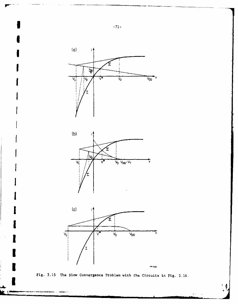
convergence. Fig 3.15(a) illustrates this problem. If the initial guess
is V0, then the first iterate solution is V1 , which is far away from the*
exact solution V . Because the derivative is large when Vk is negative, so
it requires a large number of iteration to converge to V Fig. 3.15(b)
and (c) illustrate the slow convergence problem with a saturated load MOS
inverter circuit and a depletion load MOS inverter circuit as shown in Fig.
3.14(b) and (c) respectively.
The above slow convergence problem can be resolved by using the piece-
wise nonlinear approach. For example, for the resistor load MOS inverter
circuit, first, the MOSFET characteristic is partitioned into two pieces as
shown in Fig. 3.16, the first piece is from -- to zero, the second piece
is from zero to +f, then the circuit can be solved as illustrated in Fig.
A3.16. The initial guess V0 is in piece II, the first iterate solution V1
Ais in piece I, so VI is chosen to be the breakpoint zero. Since V2 is
within piece II, the Newton-Raphson method is used to find the solution V
Remark: In the iteration scheme for MOS circuits, the piecewise nonlinear
approach is used for VDS. The change of VGS and VGD are limited by 1V at
each iteration. I3.7. Discussion I
Two large circuits were used to test the piecewise nonlinear approach,
one is a bipolar circuit as shown in Fig. 3.17, the other is a MOS circuit
as shown in Fig.3.18. The data are given in Table 3.2. The results show
that this method improves the convergence property of the basic I
I -71-
Ii (b)
I I v. Vo-VT 'I(C)
-i; V'O VDD V
F . 3
I
II1I
1 VI
II
Fig. 3.15 The Slow Convergence Problem with the Circuits in Fig. 3.14.
!A

-72-
.
U.
0
0
0.
S.' .
00
0
a U
w 04
ID

1 -73-
4K 1.4 K 100 ±4K 4KJ I.AK 100 ,5
II17
:0
I 7'
II
IT
:11

+11 -74
C-,,
T~f~ T0
00
xx
.q 0
Aw.
C,

1 -75-
UI
3 Table 3.2 Comparison of the Results betweenthe Piecewise Nonlinear Approach(PWNL) and SPICE2.
ICircuit Number of iterations Number of iterationsiE'WNL) (SPICE2)
I Fig. 3.17 34 48
Fig. 3.18 10 28
IIIIIIIIII
[i

-76-
Newton-Raphson method; however, the proof of the global convergence
property or the conditions for global convergence have not yet been
derived. More research work on this topic is needed.

I -77-
IIV. NUMERICAL INTEGRATION
IA numerical integration method is required to determine the transient
I response of a circuit. In order to make the numerical integration more
i accurate and efficient, some method of dynamically varying the timestep is
needed, this is usually accomplished by a local truncation error (LTE)
timestep control.
Let us denote the upperbound on the local truncation error by ET. In
previous work, ET was established as follows [36]. First, a maximum
I allowable global truncation error GE and the solution interval T aremax
specified. An assumption that this global error is distributed uniformly
within T is made, then the maximum allowable ET per timestep (h) is given
f by
ET - amaX * h (4.1)T
The LTE timestep control with trapezoidal integration is implemented
as follows. First, the timestep h and tn+1 = tn + hn are determined, the
solution at the timepoint tn+1 is found, then the local truncation error
(LTE) is evaluated by Eq. (4.2).
LTE = * h) 3 DD3 (4.2)12 T-
I where DD3 is the 3rd divided difference [] and tn T < tn+I . The kth
divided difference is defined by the recursive relation
DDk'l(tn+l) - DDk'l(tn) - X(tn+) X(tn)DDkk , DD1 (4.3)
i-I hn+-ii n
If LTE > ET, then the timestep is considered too large, hn is rejected, a
new h. is computed using

-78-
2 2*GEM xn T*DD3 (4.4)
and then a new timepoint t is determined. If, on the other hand,n+l
LTE < ET, then the local truncation error at timepoint t n+ is considered
satisfactory, and the timestep h is computed usingn+.
22*GEmax (4.5)
h n-I-i T*DD3
4.1. Problems with Previous Work
When the above strategy is applied to determine the transient response
of a circuit, there are two problems:
(1) SinceoDD3 is only an approximation of x(T), whenever the timestep
is changed or the input signal changes abruptly, our investigation shows
that DD3 becomes an inaccurate estimate of LTE. This inaccuracy results in
the following unwanted situations. One situation is that at the timepoint
n+19 if LTE < ET, the timestep hn+1 is increased, but at the next
timepoint tn+2, due to the inaccuracy, LTE is now found to be larger than
ET, so this timepoint is rejected and the timestep is reduced. The other
situation is even worse. If, at the timepoint tn , the input changes
abruptly, then due to the inaccuracy of the DD3 approximation to x(T), LTE
may be greater than ET and the timestep is reduced. Sometimes this happens
repeatedly until the timestep becomes too small and the program terminates.
These two situations are explained in detail later.
(2) For digital circuits, the total solution time T may consist of
several switching intervals. If a stable numerical integration method is
used, initially in an interval the local truncation error accumulates and
the global truncation error (GE) increases, but as the solution nears
.1

* 79-
I steady state in a given switch interval the global error decreases, and as
g the solution approaches the steady state the global error goes to zero, so
that the upperbound ET given by Eq. (4.1) is too conservative. This is
3 illustrated in Fig. 4.1.
3 Now we will consider the above two problems in more detail. The first
situation of the first problem can be illustrated by a simple RC circuit as
I shown in Fig. 4.2. In order to simplify the analysis, the backward Euler
method is used. The exact solution for this circuit is
v(t) = 5e-t/T (4.6)Ithe solution obtained by the backward Euler method isI v
nv n+1 " nI hn (4.7)
I where v 5V.0
I The local truncation error estimates at timepoints tn+l and tn are
I LTE h2 * DD2+ (4.8)LTn+I n l
n-LTE =h 2 * DD2 (4.9)n n-I n
where DD2nl Vn+Ih -v n v n h n v n-l
h n + h n -I.I hn+°V - V -
DD2 V v n - Vn-I Vn-2In h n- h hn- 2
n n -
n-A-
II
.M,

-80-
0
0c
A.i
I-aIx/w
0 0E/
wI// 0
/ U,
AMLJ

U -81-
II
I R _
I v(O)=5V
iI I= VM -=C2n
I
tn tn I
n nh h I
(b) FP-7007
Fig. 4 .2(a) Simple RC Circuit.
(b) Waveform of the Simple RC Circuit.
III
I- - .... ,---- -- -

-82- 1
Let us consider the situation when hn-2 = h h and hn ah, where
a is a ratio constant. From Eqs. (4.7), (4.8) and (4.9), we obtain
LTEn 1 DD2 n+i 22 2-- l n+ n 2a 2 i
- *a(4.10)LTEn n 2 a+ 1 + ah
n-1 T
If both LTE and LTE are good approximations of the true localn+1 n
truncation errors, then from Eq. (4.6), (4.7) and the definition of local
truncation error [36] the ratio of LTEn+l over LTEn should be
LT++ 1 a2n
LTEn+1 2 1 (4.11)
LTEn +ah
Comparison of Eq. (4.11) with Eq. (4.10) shows that the ratio computed by2a
Eq. (4.10) is wrong by a factor of a-. When a = 1, that is, the timestep
is constant, then the estimation by Eq. (4.8) is good. When a is
different from 1, then the estimation by Eq. (4.8) is not good. Table 4.1
gives the simulation results of the simple RC circuit, which confirms the
above conclusion. The ET used is 10 3V. At the first three timepoints,
the timesteps are kept constant, so the estimation by Eq. (4.8) is good.
At the fourth timepoint the timestep is increased by a factor of two. The
true local truncation error is 0.8930E-3, which is an acceptable error;
but the estimation by Eq. (4.8) is 0.1207E-2, which is larger than ET, so
the timepoint is rejected.
Now we would like to see if this inaccuracy can be explained by the
above conclusion. The ratio of the estimation at the fourth timepoint over
the estimation at the third timepoint is
LI

-83-
I
Table 4.1 Simulation Results of the Simple3 RC Circuit.
ITrue local
t(ns) h(timestep) LTE(estinate) truncation error
1.5 0.25 0.2355E-3 0.2339E-3I1.75 0.25 0.2332E-3 0.2314E-3
i 2.00 0.25 0.2309E-3 0.2293E-3
2.50 0.50 0.1207E-2 0.8930E-3
I
II[

-84-
0.1207E-2 5.227 (4.12)0.2309E-3
instead of 4 as predicted by Eq. (4.11). However, note that for a 2
2a . 4 133 5.227 (4.13)a+1 3 4
Eq. (4.13) shows that the estimation of local truncation error is really2a
wrong by a factor of- as shown in Eq. (4.10).a+, ssow nE. 41)
Now let us consider the second situation of the first problem. This
situation can be illustrated by a simple RC circuit as shown in Fig. 4.3.
Again the backward Euler method is used here for the simplicity of the
analysis. The exact solution for this circuit is
5e- T t tn
v(t) - (4.14)
e- t/T + 5( •-(t - tn )/T tvn - n
the solution obtained by backward Euler method is
k<n
vk+1 = I(4.15)
vk
1 + hk/T + I+hk n
where v = 5V.0
In the early version of SPICE2, when tn exceeded a source breakpoint,
then h was reduced such that the value t coincides with the breakpoint.n-I n
The timestep was reduced to a small value and then the iteration was
-i ;.1It

I -85-
K I R
+ v(O)= 5VSC V(t) r:RC=25nsI "
(a)I )
I 5V
I '
tn t
I (b)
I 5V
, 5V
IV.
tn.2 %-? I tnZ.
1 r -Htn
h h obh
(C) PP-,027
Fig. 4.3(a) Simple RC Circuit.
I (b) Waveform of vin.(c) Waveform of v.
I FL 7-

-86- 1I,
continued. Let us consider the situation when han2 h, hn 1 : ah and
h = bh! where a and b are ratio constants. From Eqs. (4.8) and (4.15), Jwe obtain the following estimate of the local truncation error:
LTE =2 2 5 + 2 (4.16)n+1 [ T(a+b)h T (a+b)
Let us also assume that bh is not small enough, so that
LTEn+1 >ET (4.17)
Then the timestep was reduced and a new timestep ch was computed by
22 b (vn - 5)
c2h 2 5(a+b)h + 2 =ET (4.18)T~a~bh T 2(a+b)
where c < b.
The local truncation error for this new timestep ch is estimated by
LIE' 2 2 5 c (V n+ 1 - 5)LTEnC+ h [ 7(a- h+ 2(ac (4.19)
n+lct ach T 2(a+c)
It follows that
ch(vn+i -5)LT '+1 a+b [1l+ 5T ]1ET -- (4.20)
ET a+c [I+ +h____"5_
5T
Since c < b then (a + c) < (a + b) and for a small enough a the ratio in
Eq. (4.20) could be greater than one. If this is the case, then the step
' .1I.'

* -87-
U size will be reduced again. This could happen again and again. This was
the case in early version of' the SPICE2 program, and frequently after
abrupt clock or signal changes the program would not converge and the job
I would be terminated prematurely.
Remark: In Eq. (4.16), the second term is an approximation to the true
local truncation error, the first term, although it is dominant, is a
Iparasitic term which is generated by the use of voltages at the timepoints
of the previous switching interval.
The second problem is detailed as follows. Let GEmax denote the
maximum global truncation error at t (Fig. 4.I). Assume that the
I ltrapezoidal method is used and that we are dealing with an exponentially
decaying waveform. The local truncation error at the timepoint t n+I is
I given by
I LTEn+1 ) n t n+ (4.21)
and for this example
I0LTEn+1 in3 Vn'max (4.22)
12T
From Eq. (4.22) and the definition of local truncation error, we obtain
-hI/T h 3
GE n+1 -GEMAX e n +n3 V n,max- GEmax (4.23)j n~max12T
where GE n+Ibis the global truncation error at the timepoint t n+. Eq.
(4.23) can be reduced toh I 3 h12T V "m GE max(_n) (4.24)
1 12j n,max max

-88-
The local truncation error timestep control requires that
h 3
LTE _2-3 V Se ET (4.25)n~l 2T3 n~mx
Assuming equality in Eq. (4.25) and eliminating hn/ in Eq. (4.24), we
obtain the following upper bound on the local truncation error.12 (GE m
ET ! (4.26)VVn , max
In order to check the above bound which was derived for RC circuits, a
number of digital circuits were simulated and the following empirical bound
on the local truncation error was -3termined.
ET 10 (4.27)VDD
where V is the voltage swing which is the supply voltage in this example.DD
Eq. (4.27) also holds for exponentially rising waveforms. Given GFmax and
VD' then ET can be determined by Eq. (4.27), and then Eq. (4.2) can be
used to control the timestep.
Eq. (4.26) shows that ET is proportional to (GEmax ) for RC circuits
if the trapezoidal method is used. In general, for RC circuits, if a stable
numerical integration method of order n is used, similar derivation as used
above can show that
ET ; (GEma x (n+l)/n (4.28)
Eq. (4.28) was verified experimentally for the backward Euler method and the
trapezoidal method. The RC circuit as shown in Fig. 4.2 was used. The simu-
lation results are given in Figs. 4.4 and 4.5.

AD-A124 064 AN INVESTIGATION OF ORDERING TEARING AND LATENCY
ALGORIT HMS FOR THE WIME-..(U) ILLINOIS UNV AT URBANA
COORD INATED SC IENCE LAB P YANG AUG 80 R_891
UNCLASSIFIED N00014-79-C-0424 F/G 9/5 NLEIIIIIIIIIIIIIIIIIIIIIIIIIIIIIIIIIIIIIIIIuIIIIIEIIIIEIIIIIIIIIIIIIIIuEIIIIIIIIIIIIuliulnD

111.0 1 LM
1111 w - jil2.2
III1 L_----" jII .
MICROCOPY RESOLUTION TEST CHART
-iiI I.. ..A.. R LA CF A -

1 -89-
II i,I, II
, 10-2-
i I
ELJ
0.-6 O-5 . 4 10 3 10-2
ET (backward Euler method) FP_03
1 Fig. 4.4 Simulation Data of the Backward Euler MethodWhich show that ET c< (GE max)2i!a

-90-
10I
30-3-
aE
LUI0
ET (trapezoidal method) F
Fig. 4.5 Simulation Data of the Trapezoidal Method
Which Show that ET o< (GE max3/2
max
... .r ,

1 -91-
I4.2. Algorithm
The following algorithm for variable timestep control was developed
I based on the discussion in the previous section. The trapezoidal method is
assumed. ET is computed by Eq. (4.27).
First let us derive an expression for the estimation of the local
truncation error which is used in the algorithm. Let us assume that
I -2 h , = ah and hn = bh. The solution obtained by the trapezoidal
method for an exponentially decaying waveform is
I -h n/2Tvn I m n (4.29)
1 +hn/2T
the 3rd divided difference is given byI
I DD2n+ 1 - DD2DD3n+I h hn_2- -+hn +h
n-2 n-1 n
3(ahb) bh (4.30)2(1a+b) 6T3 (1 _ L -- ( + L bhI 2T (1 2T' 2T
where 3(1+b) is the error factor in the estimate of the third2(1+a+b)
derivative caused by varying the timestep.!By taking into account the effect of different timesteps, the expression of
local truncation error is given by
h 3
LTE n 3 2(1+a+b) (4.31)ITn+I - 2 n+l * 3(1+b)
[ -~ -F

-92-
or we can define a new quantity DD3' which is given by
DD2n+L DD2nDD3' . =- .--- (4.32)
n+1 (h n-2 +hn)
nnthen Eq. (4.31) can be reduced to
LTE - * DD3+ (4.33)
Algorithm:
(1) Record the initial time to, final time tf, minimum stepsize hmin '
maximum stepsize h , and source breakpoints.max
(2) Set the initial timestep h = hmin"
(3) Compute X1 at tj = to + h, X2 at t2 = t + 2h, and X3 at
t 3 = t0 + 3h.
(4) Set n z 3 and compute LTE by Eq. (4.33).
(5) Compute hn = h - . If hn < 0.6h, then h = hn and go to (3);
otherwise, continue.
(6) Compute tn+1 = tn + hn . If in+1 does not exceed a source
breakpoint, then go to (7). If tn+1 exceeds a source breakpoint, then hn
is reduced such that the value t n41 coincides with the breakpoint. Compute
Xn+ 1 for this breakpoint. Compute LTE by Eq. (4.33), compute hn+, if
hn+ 1 < o.6h n , then hn z hn+1 and go to (6); otherwise, set h hmin and
to 2 tn+i, then go to (3).
. . .. .-.. ..-

-93-
(7) Compute Xn+ 1. Compute LTE by Eq. (4.33), compute h n1 , if
ht+1 < 0.6hn, then he = hn+, and go to (6); otherwise, continue.
i (8) If t > tf, then stop; if not, then n = n+1, and go to (6).
I Remark: The above algorithm has been derived for a fixed order variable
stepsize method which uses the trapezoidal rule. Our simulation results
I show that the problems we mentioned before in this chapter are resolved by
1 this algorithm. If other fixed order methods are to be used, then the
corresponding equations should be modified.
IIIII
.1
,1
!-- __ 7

-94-.
V. TEARING METHODS AND SPARSITY CONSIDERATIONS FOR NODE TEARING METHOD
There are two kinds of tearing methods - the branch tearing method and
the node tearing method. The idea of branch tearing was first introduced
by Kron (12]. Recently Chua and Chen (163 have shown that the branch
tearing is just a special case of generalized hybrid analysis. The main
idea of branch tearing is to select a set of tearing branches first, then
the given network is torn apart into several subnetworks by removing these
tearing branches (Fig. 5.1), analyzing each subnetwork separately, and
obtaining the solution of the entire network by combining the solutions of
the subnetworks via the tearing branches. Algebraically, this method is
equivalent to a particular ordering of the hybrid analysis equations such
that the resulting matrix has a bordered block-diagonal structure (Fig.
5.2). Each block corresponds to a subnetwork, and the border corresponds
to the interconnections of the subnetworks.
The idea of node tearing was first introduced by
Sangiovanni-Vincentelli, Chen and Chua £20). The main idea is to select a
set of tearing nodes first, then the network is torn apart into several
subnetworks by removing these tearing nodes (Fig. 5.3), each subnetwork is
analyzed separately, and the solution of the entire network is obtained via
the tearing nodes. Algebraically, this method is equivalent to a
particular ordering of nodal analysis equations such that the resulting
matrix has a bordered block-diagonal structure (Fig. 5.14). Each block
corresponds to a subnetwork, and the border corresponds to the
interconnections of the subnetworks.
111. 7

-95-
clJ
C
.00
1 00
C.4
En .

-96-
v
Y11 o Al
000 2 2 t2
33 t3 3
T AT T Z ATl U N t A rt ~t
Art vr
Fig. 5.2 Bordered Block-Diagonal Matrix Formulated
by Branch Tearing.

I -97-
Suntok1ISbewr
Th etothIewr
It ,
SuntwrI
FPI70Fi.53 EapeoI ewokPriindit he
Suntok yteNd ern ehd

-98-
Y ~yV
122 t20
133 Y-t33
!it _y2t 13t itt Yt Z0 y Y y v
0rt Yrr
Fig. 5.4 Bordered Block-Diagonal Matrix Formulated
by Node Tearing.
.1 t

-99-
I Recently, because tearing methods possess several advantages over
conventional circuit analysis methods, a lot of effort has been devoted to
£ the study of tearing methods for the analysis of large scale circuits. The
advantages of tearing methods are as follows: First, tearing methods are
suitable for the exploitation of the repetitiveness of a limited number of
subnetworks; secondly, tearing methods are suitable for the exploitation
of latency; thirdly, tearing methods are suitable for parallel processing.
IIn order to solve the network by tearing methods one must specify a
Ipartitioning strategy, and also one must specify a technique for solving
the partitioned equations. In the literature mostly the branch tearing
Umethod has been used to solve large networks 122-24]. The solution
strategy has been to estimate the current or voltage at each tearing port
i and to excite the torn subnetworks with independent sources at these ports.
The remaining port responses are computed, and are substituted into the
6 interconnection equations. If these equations are not satisfied, then
another estimate is made of the variables chosen as port excitations. This
iterative procedure continues until convergence is achieved. If the
subnetworks are nonlinear a multilevel iteration scheme is used, such as a
Gauss-Seidel [22], Newton-SOR [24] or a multilevel Newton iteration [42].
However, the first two iteration schemes do not have second-order
convergence while the third scheme requires the computation of an
add-itional Jacobian matrix.
Because the above approach introduces new variables, such as tearing
1 branch currents, the complexity, of the problem is increased. Also, a
multilevel iteration scheme is required. Another disadvantage of the
I branch tearing method is that each subnetwork must contain the datum node
for the network, or else a local datum node must be chosen for each
subnetwork. In the program SLATE a different approach is used, and the

-100-
internal subnetwork variables are eliminated from the tearing node
equations. Then the tearing node voltages are computed. Only a one level
Newton iteration is required, and the internal variables for each
subnetwork can be eliminated using parallel processing methods. The
elimination of the internal variables is equivalent to replacing the
subnetworks by Norton equivalent circuits at the tearing nodes.
In our study of tearing methods it was assumed that the user specifies
the subnetworks, and any part of the network not specified as a subnetwork
is automatically included in the subnetwork called rest of network in Figs.
5.1 and 5.3. The subnetworks are processed first in the solution
algorithm, and the tearing branches or nodes along with the rest of network
equations are processed last. Thus, the branch tearing method and the node
tearing method described in Section 5.1 and Section 5.2 are somewhat
different from those found in the literature r12-141. T, Section 5.3, a
comparison between branch tearing and node tearing is given. In Section
5.4, the derivation of the construction of the node tearing matrix from
subnetworks is detailed. The sparsity considerations for the node tearing
method are presented in Section 5.9. The implementation of node tearing is
described in Section 5.6. The circuit interpretation of the tearing
methods is given in Section 5.7. Some conclusions are given in Section
5.8.
5.1. Derivation of the Branch Tearing Method
Let N be a connected network having (n+1) nodes: the datum node n0
and the nondatum nodes o = ln,,n 2 . .. . .. 9nn , and b branches,
S1bi9b2 .. . .. .. bb. Let the branch voltages, branch currents and the
Tnode-to-datum voltages be denoted by e (e i e ..... e )
-. e 9 b'
A.- d1

1 -101-
(i i 2 . . . . . . i ) and v (v,v 2 . . . . . . V) respectively. Let the
interconnection be defined as the remaining part of the network when all
the subnetworks are removed, that is, the set of tearing branches and the
I rest of the network in Fig. 5.1. Let us aasume that a proper set of
g tearing branches has been chosen such that there is no mutual coupling
either among the torn subnetworks or between the torn subnetworks and the
interconnection, and that all subnetworks contain the common datum node.
This latter assumotion is made in order to avoid floating subnetworks which
I result in singular submatrices. The more general case when all subnetworks
g do not contain a common datum node is discussed in r17]. Subscripts s, t
and r are used to denote quantities pertaining to the subnetworks. the
tearing branches and the remaining branches, respectively, so the branch
set 9 is partitioned into three subsets 8s, St and Sr (Fig. 5.1), and the
node set C is partitioned into two subsets csand r. This yields the
jfollowing special structures for the reduced incidence matrix A and the
branch ionductance matrix G of network N:
SB S r
A S (5.1)Of 0 A A5
s t r
G 0 0s -3 S
G t o G 0 (5.2)
r 0 _O*
ti

-102-
Let the torn network have k subnetworks Ni, N2 , . .. . .. ,Nk. Let os
and 3s be partitioned correspondingly into k subsets oi (29 ...... 1Qk and
S i t a2, ...... 9ak respectively. With this partitioning, the node-to-brancn
incidence matrix A can be written as
1 2 .... k Otof t A tl
Qe A 0
A • 0 (5.3)
0 .
k Ask A tk
1r 0 Art ,Arr\II
I /
the branch conductance matrix G can be written as:
33 a .3 131 2 k t r
13 G01I '.sl
2 os2 _
G 0 0 (5.4)
* 0 I
k 2 skI
0 ;Gt 0-- o- --3t 0 'SOrG
r o
A -
J

-103-
IThe network variables are constrained by the Kirchhoff's current law
I (KCL), Kirchhoff's voltage law (KVL) and the branch constraint relations
(BC) [28).
(KCL) A i + A t = 0 (5.5)
A i + A i r 0 (5.6)
(KVL) e = A Tv (5.7)
AT-- ATv + v (5.8)-t -,,s -r,-r
T T
A A T v (5.9),%.r Zrr r
(BC) i = I + Gspe- Gges (5.10)
t ~t s + z- t -Z;.-t S5tt
i=I + G e G e (5.12)~--r "-r S ,,P--r "~v ,,Es
Substituting Eqs. (5.7), (58) and (5.9) into Eqs. (510) and (5.12), and
then substit-iting the results into Eqs. (5.5) and (5.6), we obtain
A G A Tv + A i=- J (5.13)
Arl A G A T V = O (5.14)rtt ~rr--rrr -rs
Substituting Eq. (5.8) into E q. (5.11), we obtain
ATv - Z i + AT v = E (5.15)-- B ,,--t -rt-r - s
where J A G e -A I
-" J :A Ge -A I-.rs -rp-v.-rs -rr,-rs

-104-
Aand E :e -Zian ts " ts " Z-ts"
Eqs. (5.13), (5.14) and (5.15) can be rewritten in the following form:
AGA T A 0 v,,9%-,SFS ~t- S ,Ss
T TA A i E (5.16)
t -C r -t -Cs
0 A A G A v J-rt-rv--v,-rr -r -rs
Let us now examine the term As Gs.AT in Eq. (5.16). Substituting A of Eq.S -S
2 Ys2
TT
A G of Eq.. 0 (5.17)
•0•
\t y
k y-sk
where Y = A G AT J=1,2 .......,k,~Sj ~s jS s) sj
so Eq (5.16) can be rewritten as:
I /
Y A tl v rl J ssl
~s2 --t2 -r2 ss2
'00 0I
0• (5.18)
Lsk .tk v k kAIT AT T I AT
-tl -t2 -tk t"Z rt t E t
-rt -r _ _rs
o -- ---- --r - -.--.---

1 -105-
where Y A vG TA Eq. (5.18) is the resulting matrix by branch tearing
method, which has the desirable bordered block-diagonal structure and it is
a particular ordering of the hybrid analysis equations.
5 I5.2. Derivation of the Node Tearing Method
Let the interconnection be defined as the remaining part of the
network when all the subnetworks are removed, that is, the set of tearing
3 nodes and the rest of network in Fig. 5.3. Let us assume that a proper
set of tearing nodes has been chosen such that no coupling exists either
5 among the torn subnetworks or between the torn subnetworks and the
interconnection. The node set a is partitioned into three subsets as , a
and ar, and the branch set 8 is partitioned into two subsets 8S and3 r
(Fig. 5.3). This yields the following special structures for the reduced
incidence matrix A and the branch conductance matrix G of the network N:I
S A 0
A a A A (5.19)t - tts -trrC1 0 A=
i rG aI s r
G - Sj (5.20)B 0r E
II.

-106-
Let the torn subnetwork have k subnetworks Ni, N 2 Y .. . .. . ' N k Let
and B be partitioned correspondingly into k subsets C11' a2 ..... ' ak
and 3 1, 8 2 .. . . . . 8 k respectively. With this partitioning, the node-branch
incidence matrix A can be written as:
a. 2..... aB I a
of AI sI
2 As2 I
A .•0 (5.21)
A I
t .tsl _.ts2 -tsk I r
r 0 -i
The branch conductance matrix G can be written as:
1 2 . r
i
I G G2 Zs2
" 0 IS 5
G '0 (5.22)
* 0
k. 2 skI
r
o -li

-107-
The network variables are constrained by the Kirchhoff's current law
(KCL), Kirchhoff's voltage law (KVL) and the branch constraint relations
(BC).
(KCL) A. = 0 (5.23)
I At£ i + A (5.24)
A- :0 (5.25)
I TT(KVL) e = ATv + A v (5.26)
e = AT v ATV (5.27)
(BC) i = I + G e - G e (5.28)~s -SS ~-SS -&SS
i = I - G e (5.29)~r .-rs -.r-r -t'-rs
Substituting Eqs. (5.26) and (5.27) into Eqs. (5.28) and (5.29), and then
substituting the results into Eqs. (5.23), (5.24) and (5.25), we obtain
A G AT + AGA T v =JS (5.30)
T T I~s~
A G ATv + (A G AT + A G AT )v + A G ATV J (5.31)tts tss-ts -tr-v.-tr - t cr.V--r~r -ts
Av T,A G~vvt + A O6v J (5.32)_tv r wr, r _rs
*1where J :AGe - &
J :A G e -A I + A G e -A I-Cs -.-- ss -Ce--ss ~tr-D-rs tprs
and J A G e - A IIPr s --,P rs S ,,-rs
Eqs. (5.30), (5.31) and (5.32) can be rewritten as:
I

-1.08-
T TA G AT A G A 0 v
T T T TAt GAs At G +It AT G A GA v 3t&..S.S.S .. S.S-..s .t r---tr r-r-r -t = (5.33)
0 AGA A G A T v Jr r t r-rr -r -rs
TLet us now examine the term A G AT in Eq. (5.33). Substituting the A of !
Eq. (5.21) and G of Eq. (5.22) into A G AT , we obtain
Ct y
1 i - 2 . . ..l.1i 4S
of2 Ys2T
AG f. . 0 (5.34)
* 0
kL Ysk
where Y. A GA T J=1,2 ........,k
so Eq. (5.33) can be rewritten as:
1 ~I -sts Jsl I v
0Xs2 o I1x9t 2 42 Js2
0 " " .(5.35)
s k tk -sk -ssk
y s ts2 . '.. tsk t-Ytt I -tr V _it
0 Y v Jrt 1rr r ,r s
, - : 000,

3 -109-
where Y = A G AT j=1,2 ...... kI -Stj -s-j.. ts
'Yrs = A G A T J=1,2, ..... k
= ~tsssj ......
I AYG A T +A T~-t t -s- S--Cs -r--Cr
,Y :A AT~rt _tr-2-r
,Y :AG-AI -rt -vZ-rC
Tand Y =A G A.
Irr -- r
Eq. (5.35) is the resulting matrix by node tearing method, which has
the desirable bordered block-diagonal structure and is a particular
ordering of the nodal analysis equations. In the above derivation the
modified nodal method could have been used. In this case the vectors v-s
and v consist of hoth node voltages and currents of branches for which an_r
admittance description presents difficulties. This is actually the
formulation used in the program SLATE.
5.3. Comparison of the Branch Tearing Method with the Node Tearing Method1As described above, branch tearing is equivalent to a particular
jordering of the hybrid equations, node tearing is equivalent to a
particular ordering of the nodal equations, so branch tearing requires the
use of tearing branch currents as extra variables. As a result of the
IIII

above property, node tearing possesses the following advantages over branch
tearing:
(1) the dimension of the matrix formulated by node tearing is smaller
than that formulated by branch tearing;
(2) the number of nonzero entries in the matrix formulated by node
tearing is smaller than that formulated by branch tearing [201;
(3) for passive networks, node tearing generates a diagonally-dominant
matrix, so any application of the Gaussian elimination method with diagonal
pivoting is stable, while this is not the the case in the branch tearing
method;
(4) usually, in the analysis at' large scale circuits, node tearing
preserves the identities of' the resulting torn subnetworks, while branch
tearing sometimes destroys the identities of the torn subnetworks.
However, one can generate examples in which the opposite is true, but these
situations were not encountered in our examples.
The above conclusions are not conclusive; although the dimension at'
the matrix formulated by branch tearing is larger than that at' node
tearing, the extra nonzero entries are either +1 or -1. If this property
is fully exploited, then node tearing may not be so advantageous. But full
exploitation at' the property that extra entries are either +1 or -1
requires a much more complicated sparse matrix technique. So node tearing
is pref'erred and is used in the program SLATE.

T I -Iii-
5.4. Constructing the Node Tearing Matrix from Subnetworks
In Section 5.2, the derivation of node tearing is given; however, in
I the real implementation we do not want to solve the whole matrix equation
at one time. We would like to process each subnetwork separately, and then
obtain the solution of the entire network by combining the results of
U subnetwork process.
I
In the following the procedure of constructing the node tearing matr.x
from subnetworks is detailed. Let us consider one subnetwork Ni . Let the
tearing nodes which are connected to Ni be denoted by oti' the node voltage
of 'ti be denoted by vti' the nodes of Ni be denoted by ai, the node
voltages of ai be denoted by vsi, and the currents which represents the
1 relationship of the rest of the network with this subnetwork be denoted by
i (Fig. 5.5). vti and Jti satisfy the following relations:
Uzt (5.36)I~ I.
E = ti 0 (by KCL) (5.37)I3.
I1I_ _ _ _ _ _ _1

-112-
To the RestSubntwok Ni4,2 of the Network
RP- 7001
Fig. 5.5 One Subnetwork.

3 -113-
IThe node equations for this subnetwork have the following form:
I i
A Kti
II
,
By augmenting with appropriate zeros to match the dimension and summing Eq.
(5.38) for all the subnetworks and the interconnection, we obtainII
ysl I s 2 -
I Ys*t s j
I.
ly V
- s 2 0 I Yst2 -s Z. 2
0 ". ""(5.39)
Ysk -stk i 2 ssk
Ytsl Yts2 4tsk I-tt I -tr -v itsI 0 4 . . .
-Irt Irr -vr a00r rs
T
I

We can see that Eq. (5.39) is identical to Eq. (5.35).
Eq. (5.39) is solved by first eliminating all theYtsi to obtain the
interconnection matrix equations.
Y tt Y r v It
(5.40)
* k )-I~
* k
an 2st = st I: Ytsi ( Ysi JS
i= 1
Eq. (5.40) is solved to obtain solutions for v t and v r , and then the
solution v . can be obtained by using backward substitution.
The above solution procedure can be modified to enable us to process
each subnetwork separately to obtain the interconnection matrix equations.
Let us consider Eq. (5.38) again, after eliminating Y s, we have
CI.I. I f ti
U L. . L.I 0S, usi I -si si -si. ~Si SSI ~0L Is " I
-W I %I +iLi L
where L U 2Y-s i.si ~Si'.
Y * Y -Ytti Ytsi __si i L -u.--- -

1 -115-
I . ~-and i i Y (
atsi = tsi - si -s i J "S
The partial interconnection matrix equations obtained from Eq. (5.41) are
=tt t = I + t (5.42)
By augmenting the above arrays with appropriate zeros to match the
dimension of Y (this is only conceptual, because sparse matrix techniques
I are used and every elment is put in the appropriate location in a one
dimensional array) and summing up Eq. (5.42) for all the subnetworks and
Ithe interconnection, we obtain Eq. (5.40) again.
Since Z J 0 by KCL, therefore J does not appear in the final
i1ti2- -timatrix equations (5.39) and (5.40), so we can neglect J. in both Eqs.
(5.38) and (5.42).
I So the modified solution- procedure is as follows:
1(1) Formulate the simplified Eq. (5.38) for each subnetwork, i.e.
i 0ti
i Si st s SSI (5.43)
(2) Process Eq. (5.43) to obtain the simplified Eq. (5.42) for each
subnetwork, i.e.I= ts (5.44)I@ tJ )

-116-
(3) Sum up Eqs. (5.44) for all subnetworks and the interconnection
with appropriate dimension match to obtain Eq. (5.40);
(4) Solve Eq. (5.40) to obtain vt and vr;
(5) Solve the upper part of Eq. (5.41) by backward substitution to
obtain V I for each subnetwork Ni.
5.5. Sparsity Considerations for the Node Tearing Method
Now let us compare different ways of sparsity exploitation for
processing Eq. (5.43). For the solution procedure discussed in the
previous section, both LU factorization and substitution procedures are
required. In SLATE the modified nodal equation formulation and the new
reordering strategy described in Chapter 2 are used at the subnetwork
level. After the current variables and the corresponding 'positive' node
voltage variables are eliminated, the final subnetwork matrix is
structurally symmetric. So here we assume that the subnetwork matrix is
structurally symmetric, under this assumption, there are two possible LU
factorization procedures we would like to compare. there are other
procedures described in 138), but these procedures are either equivalent to
them or are less efficient.
The two LU factorization procedures are denoted by F1 and F2 £38), and
are given in Table 5.1.
-1
whereL U ' V LZs k-s k -sk' - sk' tk'
T A1 i -1W = Y UV
- ts1k'k - sl
and LtkUtk :ttk : ttk "tskUsWs 2 stk '
-Aft

3 -117-
" II
I Table 5.1 Possible Factorization Procedures.
I
I F 2
i Lk u -sk k sk 0 1 vIT Ltj 0lok s L k 0 Utk
I
III
I
.I[ 2,

-118-
In Fw only those rows of hich are required to compute V are2' onytoeroso Vreq ~computed, V consists of those rows of V corresponding to the nonzero
columns of Ytsk"
Let 1.1 denote the number of nonzero elements in a vector or a matrix,
and M(.J) and M(J.) the jth column and the jth row of matrix M,
respectively. Let nt denote the number of tearing nodes, and B(k)
satisfies the following relation.
r k=O
B(k) = (5.45)
1 k 1, k integer
The following lemmas are used to compare the number of operations between
F and F2.
Lemma 5.1. Suppose the subnetwork matrix is structurally symmetric, then
the number of rows of [ equals the number of nonzero rows of V.-req
Proof: From the definition of V p, we know that any nonzero row of V which
is not a row of V must consist of only fill-ins. Suppose it is row i,
then there must be a nonzero row j of V , J < i, and a nonzero L Row
j together withLskij creates the fill-ins of row i. Due to structure
symmetry, there also must be a nonzero U sk,ji So in order to evaluate the
row j of Vp, it is necessary to evaluate the row i of V.
Lemma 5.2. Suppose the subnetwork matrix is structurally symmetric and Y
is mxm, then the difference in the number of operations between F1 and F2
(DNF) is:

DNF = LI v- ) t I I (l5 () 1I(j.)l :(j=1 j.1
U j=2 i-j+1 j
if V rqis full, thenr eq
DNF Lj-i) t~.(i-)I - E dL 8ki) -1)n- 1y(iiI)B(Iy(i.)I)j21. j.1
t- yLtskl (5.47)
5Proof: DNF E (J .~ - 1)IW(j.)I + z IwT(.j)I Iv(i)I
j=2 i~jl re j=1 req
E E~i1 -u6~iI~ e~-I-Z ys -~j e j (5.49)
From steutua 5.1, ety obtain ai
I IW~req - 2 !V-)I Bjy(*) (5.52)
Sustttn Eqs (5.9) (5.0) (5.51) an(55)5noE.1
(5.48)ma5., we obtainEq (54)
-req
Substituting Eq. (5.53) into Eq. (5.46), we obtain Eq. (5.47).

-120-
Associated with F and F,> there are five possible substitution
procedures denoted by Si , Sl, S1 , S2 , and S. [38] which are given in
Table 5.2, where b req consists of the rows of b which are required to
compute b . bp are those rows of b corresponding to the nonzero columns of
-p -p- tsk"
Let C(.) denote the number of operations required in performing a
given procedure S. By comparing the entries of the five substitution
procedures in Table 5.2, the following equation is obtained.
C(S1 ) - C(S) C(s 2 ) - C(S 2 )(.54)
In large scale integrated circuits, most of devices are nonlinear.
Due to the current sources generated by Newton-Raphson iteration and
numerical integration, it is reasonable to assume that the source vectors
4ssk and 4tsk are full. Also, since Vsk and Vtk are the required node
voltages, it is reasonable to assume that they are full. Under the above
assumptions, we obtain the following lemmas.
Lemma 5.. a, b, y, and ^ are full.
Lemma 5.4. Suppose that the subnetwork matrix is structurally symmetric,
then the number of rows of b req equals the number of nonzero rows of V.
Lemma .j. Suppose that that subnetwork matrix is structurally symmetric
and Y sk is mxm, then the difference in the number of operations between S1
and S1 (DNS1) is:
-I

IIC'rn2
N (n W w
U).0 z
it Qi) 4-bI
I4 -- W ~02 0
11 0d4
>4 -'-
UUrn -W
Z ~W202I
I "-4
I1 N
I 414/2
02 02U tfn
IWI

-122-
DNS1 = C(S1 ) - C(S1 )
m mm
='1 Vsk j=l'-tskm
=IV1-l Y s I -!: (JUsk ( j ) I - 1 ) B ( Qj ) I
m
=(number of fill-ins in V) - (IlUsk(j.) l-)B(V(j )I) (5.55)
Lemma 5.6. Suppose that the subnetwork matrix is structurally symmetric
and Ysk is mxm, then the difference of number of operations between S1 and
S I (DNS2) is:
DNS2 = C(S1 ) - C(SIn t n t m
" DNS1 j I'V('j)I-jIIY tk('J) II L sk(.'B(IV(j')m m
DNS1 lvl-lYtskl-j--l" (lusl,(J') -I)B((V(J')[)-j-B(fV(j.)I)m
2DNS1 - IVB(jV(j-)I) (5.56)
Remark. From Lemma 5.6 we can conclude that if C(SI) < C(SI) then
C(Si) < C(S1 ), that is, only when C(S1 ) > C(S1 ) do we need to compare Sl
with Sr*.
eMa 5.7. Suppose that the subnetwork matrix is structurally symmetric
and Y is mxm, then
C(S1*) < C(S 2 ) (5.58)
Proof: From Eq. (5.54), we obtain
* _ . . . . .
bA

r -123-
C(S1) 1 C(S2) =C(S) C(S2 ) (5.59)
So we only need to prove C(SI ) - C(S2 ) < 0
+M
=j-l(IUsk(i) -1)(B(IV(J')I)-Z 2 (j ) I) (5.60)
SinceI I (j) I-B(IV(j
" I[) (5.61)
andIz2(j) IlIz4 (j) 1 (5.62)
so we have
[ IZ (j ) I B ( V ~j ") 1) (5.63)
Substituting Eq. (5.63) into Eq. (5.60), we obtain
C(S*) - C(S*) " 0 (5.64)
From Lemma 5.7, we know that S2 and S2 are not as efficient as the
other procedures, so they are eliminated from the list of possible
substitution procedures. Now we are left with S1 , S1 and S. The
* possible combinations of factorization methods and substitution methods are
F1 + Sl, F1 e+ SI, F1 + S1 , F2 + SI , and F2 + S1 . Theoretically we can
not eliminate any of these five combinations, because we can always come up
with a special subcircuit structure for which a particular combination
gives the best result. However, after conducting a large number of
Ir studies, we found experimentally that F1 + S,. gives the best results for
A all the practical circuits we used; moreover, F1 + S1 is well compatible
A.
- - ... 1... .. 9,

I-124-
1with the sparse matrix techniques and is the easiest one to implement, so
F1 + S I was chosen to be used in the program SLATE.
In the following we would like to present a small selection of the
examples which we have analyzed by using Lemma 5.2, Lemma 5.5 and Lemma
5.6.
Example 5.1. The subcircuit used is a TTL two-input NAND gate with
parasitic resistors included (Fig. 5.6). The admittance matrix for this
subcircuit is shown in Fig. 5.7.
DNF = 20 - 23 - 39 = -42
DNS1 = 9 - 13 -4
DNS2 -8 - 10 = -18
so the best combination for this subcircuit is F1 s S1 .
Example 5.Z. The subcircuit used is an ECL two-input NOR gate with
parasitic resistors included (Fig. 5.8). The admittance matrix for this
suboircuit is shown in Fig. 5.9.
DNF = 17 - 15 - 27 = -25
DNS1 = 6 - 8 = -2
DNS2 -4 - 6 - -10
so the best combination for this subeircuit is F. + SI .
Example The subcircuit used is an MOS two-input NAND gate with

3 -125-
III
I 28
I 1726 24 23 1-61 16
1218
8
91 21
I 52
11I5
I F5-oO03I Fig. 5.6 TTL Nwo-Input NAND Gate.
I

-126-
t-~ 00000000000000 x x. 0 0 0 z-, 0 Z
C','
C,,'
C',4
C','
C','
C"C
0 CD0ID00c0 000 XX000X0C
00000000000000 0000000000 00
~~00 o~o oo0 oZZ0 000~ 00 00
C14
- 0

U -127-
I7I9
I!I
17 14 1113 5 21
19 iis0151 10 23
44
16
22
FP- 7014
T Fig. 5.8 ECL Two-Input NOR Gate.
4,

-128-
23 22 5 6 3 8 7 9 10 11 12 4 14 15 16 17 IS 13 2 19 20 21(5) 23 1 0 X 0 0 0 0 0 X 0 0 0 0 0 0 0 0 0 0 0 0 0(6) 22 0 1 0 X 0 0 0 0 0 0 0 X 0 0 0 0 0 0 0 0 0 X
(23) 5 0 0 1 0 0 0 0 0 0 0 0 0 0 0 0 0 0 0 0 0 0 0(22) 6 0 0 0 1 0 0 0 0 0 0 0 0 0 0 0 0 0 0 0 0 0 0
30 0 00 xO0 0 00 xO 00 00 00 00 00 008 00 0 00 X XXO0 00 00 00 00 00 00 07 00 0 00 X X X0 000 00 0 00 0 x00 090 00 00 XX X 000 00 0 00 00 F 0X
10 0 0 X 0 0 0 0 0 X X X0 0 0 0 0 0 0 0 0 0 011 0 0 0 0 X 0 0 0 X X X 0 0 0 0 0 0 0 0 0 0 012 0 0 0 0 0 0 0 0 X X X X 0 0 0 0 0 0 0 0 0 04 00 0 X 0 00 00 0 X O 0X0 0 XC 0 00 00
14 0 0 0 0 0 0 0 0 0 0 0 0 X X 0 0 0 XX 0 0 015 0 0 0 0 0 0 0 0 0 0 0 X X X 0 0 F X F0 0 016 0 0 0 0 0 0 0 0 0 0 0 0 0 0 X X X 0 0 X 0 017 0 0 0 0 0 0 0 0 0 0 0 0 0 0 X X X 0 X F 0 018 0 0 0 0 0 0 0 0 0 0 0 X 0 F X X X F FF 0 013 0 0 0 0 0 0 0 0 0 0 0 0 X X 0 0 F X FF X 02 0 0 0 00 0 XF0000X F 0X F F XFF F
19 0 0 0 0 0 0 0 0 0 0 0 0 0 0 X F F F FX F F20 0 0 0 0 0 0 0 0 0 0 0 0 0 0 0 0 0 X FF X F21 0 0 0 0 0 0 0 X 0 0 0 0 0 0 0 0 0 0 FF F X
Fig. 5.9 Admittance Matrix for the Subcircuit in Fig. 5.8.

1 -129-
I parasitic resistors included (Fig. 5.10). The admittance matrix for this
3 subcircuit is shown in Fig. 5.11.
DNF 18 - 9 - 30 = -21
DNS1 3 - 5 -2
DNS2 = -4 - 7 = -11Iso the best combination for this subcircuit is F1 + S1.
These three examples show that at the subnetwork level the best
combination is F1 + S1 .
jFor the interconnection matrix, because this matrix has the same
property as that of the matrix formulated by the MNA for any circuit, so
jthe new reordering strategy of the MNA and the Markowitz sparse matrix
scheme are used to exploit the sparsity at this level.I1 5.6. Implementation of the Node Tearing Method
As concluded in the previous section the best combination at the
subcircuit level is in most cases F1 + Sl, now we would like to describe
jthe implementation of this approach. First, at the subcircuit level, the
source vector is appended to the matrix to form
!.V~k jstk Jssk'
1tsk ittk tsk (5.65)
Secondly, use the new reordering strategy of the MNA and the Markowitz
I sparse matrix scheme to find the LU factorization Of Isk. The LU
I AJ

-130-
2
3
4
P P-7015
Fig. 5.1I0 MOS Two-Input NAND Gate.
, i! -
8 l , ,

I I -131-
Ii
!!
13 2 5 4 8 9 3 7 6 10 11 12(2) 13 1 X 0 0 X 0 0 0 0 0 0 0
(13) 2 0 1 0 0 0 0 0 0 0 0 0 0
5 0 0 X X 0 0 0 0 0 0 X 04 0 0 X X 0 0 X 0 0 0 X 0I 8 0 x 0 0 x x 0 0 0 0 0 x
i9 0 0 0 0 X X 0 0 0 0 0 X
3 0 0 0 X 0 0 X X 0 0 F 07 0 0 0 0 0 0 X X X X F 0
.6 0 0 0 0 0 0 0 X X X F X10 0 0 0 0 0 0 0 X X X F F
11 0 0 X X 0 0 FF F F X F
12 0 0 0 0 X X 0 0 X F F X
III
Fig. 5.11 Admittance Matrix for the Subcircuit in Fig. 5.10.
IIIIII

-132-
factorization operates on the whole matrix but terminates after the LU
factorization of Ysk is obtained. Now the original matrix is transformed
into I I
Lsk -sk -stk I-sk -ssk
(5.66)
Y*gZtsk Esk Lttk
Thirdly, formulate the interconnection matrix equation (5.40). Fourthly,
use the new reordering strategy of the MNA and the Markowitz sparse matrix
scheme to find the LU factorization of Eq. (5.40), and use forward and
backward substitution to find the solutions for vt and vr" Fifthly, use
backward substitution to solve the upper part of Eq. (5.46) to obtain the
solutions V~sk"
Remark: The reordering of the subnetwork and network matrix equations is
done in the preprocessing phase. The subnetwork matrix equations are
reordered first. So when the network matrix equations are reordered, the
structures of all the Y 's are known. From the structures of all the Y tkttk
and the circuit description of the network, we can reorder the network matrix
equations by the new reordering strategy of the MNA and the Markowitz sparse
matrix scheme.
: L ........... 1 P

1 -133-
I5.7. Circuit Interpretation of the Tearing Methods
Although the derivations of the tearing methods are quite
I mathematical, there is a very simple circuit interpretation. The node
tearing method is just a generalized Norton equivalent circuit approach.
II The branch tearing method is just a generalized Thevenin eqivalent circuit
I approach.
Let us consider node tearing first. Consider the special case when
there is only one tearing node. The partial interconnection matrix
jequations (Eq. (5.42)) that we obtain for each subnetwork are just the
Norton equivalent circuit matrix equations for that subnetwork. This is
illustrated in Fig. 5.12(a). So for the case when there are more than one
tearing node, Eq. (5.42) is just the generalized Norton equivalent circuit
I matrix equations for each subnec. See Fig. 5.12(b) for an illustration of
the case of two tearing nodes.
Now let us consider branch tearing for the special case when there is
only one tearing branch. The partial interconnection matrix equations that
we obtain for each subnetwork are just the Thevenin equivalent circuit
matrix equations for that subnetwork. This is illustrated in Fig.
15. 13(a). So for the case when there is more than one tearing branche, the
partial interconnection matrix equations that we obtain for each subnetwork
are just the generalized Thevenin eqivalent circuit matrix equations for
that subnetwork Fig. 5.13(b) illustrates the case of two tearing branches.
i- - - - II - I I ... . . . . . . . ...... ... - - - - - ---- i . . .. . -II .. .....

-134-
o
00 c00 ca
00z0
u
c0
0
0
04

-135-
N N 0
ooo~po
C-r
000
to
0))
U-41
OILI
3U 0r 0
I

-136-
5.8. Discussion and Conclusion
The reason why we considered many possible LU factorization and
substitution procedures at the subnetwork level is that at the subnetworkc
level we only want to perform Gaussian elimination for the variables v sk
and the elimination procedure terminates after the LU factorization of Y s
is obtained. At the interconnection level, because we perform the Gaussian
elimination for all the variables, only one LU factorization and
substitution procedure is used.
As discussed in Section 5.5, it is possible to generate special
subcircuit structures for which some other combinations give better
results, however, our experimental results show that even for these
specially constructed circuits the difference of the number of operations
is only 1 or 2 most of the time, so this very small savings does not
justify the extra difficulties of implementation associated with these
other combinations; moreover, for all the practical circuits we tested,
F + S showed considerable savings over all the other combinations.

-137-
VI. LATENCY EXPLOITATIONIIn conventional circuit simulation programs [1,2], all of the node
3 voltages or branch voltages and currents are calculated at each iteration
and each timepoint. Even with sparse matrix techniques the simulation of
modern large-scale integrated (LSI) circuits is not possible in many
j situations due tc the excessive computation time and high storage
requirements. The latency approach is a circuit analysis version of the
selective trace approach used in logic simulation. This approach takes
advantage of the fact that in some circuits only a small portion of the
circuit is active at any given time and at any iteration, and t us provides
savings in CPU time.
In the program SLATE this approach is applied at three levels: (1)
device level; (2) subnetwork level; (3) network level. At the device
* level, it is also called the bypass scheme. This scheme is done by
* monitoring the operating point :2 each nonlinear device. If the operating
point does not change significantly between timepoints or Newton-Raphson
iterations, then the device models are not reevaluated, and the matrix
entries computed at the previous timepoint or the previous iteration are
used again. This scheme is used in SPICE2 [2] and SPLICE [39]. Latency at
the subnetwork and network levels can be well exploited when tearing
methods are used to analyze the network. The tearing method used in
I program SLATE is node tearing, so in the following discussion about latency
at the subnetwork and network levels, node tearing is assumed. Latency
I exploitation at the subnetwork level is presented in Section 6.1. Latency
exploitation at the network level is presented in Section 6.2. In Section
6.3 a discussion is given.

-138
6.1. Latency Exploitation at the Subnetwork Level
As discussed in Chaoter V, the node tearing method is just a
generalized Norton equivalent circuit aporoach. After all the internal
circuit variables of a subnetwork are eliminated, a generalized Norton
equivalent circuit of the subnetwork is obtained. Combining the equivalent
circuits of all the subnetworks with the rest of the network (Fig. 6.1),
we obtain the interconnection circuit. So after applying the node tearing
method to tear the network apart into several subnetworks, the
preprocessing of each subnetwork to obtain the contribution to the
interconnection matrix is equivalent to constructing an equivalent circuit
for each subnetwork. If the solutions of the circuit variables of a
subnetwork do not change significantly between timepoints or Newton-Raphson
iterations, then there is no need to reconstruct an equivalent circuit for
that subnetwork. The equivalent circuit constructed at the orevious
timepoint or the previous iteration is used again and the subnetwork is
declared as latent. The subnetwork remains latent until the solutions of
the circuit variables of the subnetwork change significantly between when
it is declared latent and the oresent time or the oresent iteration. This
is the basic concept of latency at subnetwork level.
There are two types of latency at the subnetwork level: one is
latency in the Newton-R~ahson iteration, the other is latency in time.
Latency in the Newton-Raphson iteration is not natural. It is related
to the convergence property of each subnetwork and the initial guess of the
operating point for each subnetwork. Let us consider the example in Fig.
6.2. It is assumed that the input signal is constant and that a ic
analysis is required. Different subnetworks may require different number

3 -139-
Suntok1IjSbewr(a?
Th etoth ewr
n, n,
Suntwr(a,3
nI
FP- 7048
Fig. 6 .1(a) A Network Partitioned into Three Subnetworks by
the Node Tearing Method.
(b) Equivalent Interconnection Circuit obtained from
the Node Tearing Method.

-140-
.Y.-
.o a.
4.41
3UC4.
w 04
00
4

of iterations to converge, for example, because the initial guess of the
operating points may be good for some subnetworks and bad for the others.
After these subnetworks converge, they are declared as latent. The
1 Newton-Raphson iterations continue until all the subnetworks converge.
I This phenomenon is called latency in the Newton-Raphson iteration. Taking
advantage of this latency results in savings in the execution time. This
j latency may not exist in some circuits. For example, a linear circuit.
Latency in time is a natural phenomenon. All physical devices have
intrinsic delay time between excitation and response. For a large network,
j qhen the input signal changes, it takes time for this change to propagate
to the rest of the network. Let us consider the example in Fig. 6.2
again. Let 'us assume that the innut changes from OV to 5-V at time t0*
Initially, probabably only the first few subnetworks are not latent, the
rest of the subnetworks are latent. As time oasses, the change in the
response propagates to the intermediate subnetworks. At this time, only
the intermediate subnetworks are not latent, the rest of the subnetworks
are latent. Finally, the change oropagates to the last few subnetworks and
the rest of the subnetworks are latent. This phenomenon is called latency
in time, and it always exists in real circuits. Taking advantage of this
Jlatency results in savings in the execution time.J In order to exploit these two tyoes of latency, some sort of latency
criteria are required to determine if a subnetwork is latent. The latency
I criteria proposed here are developed for the node tearing method, if the
branch tearing method is used, these criteria should be modified
accordingly.
I

-142-
Let us consider one subnetwork Nk. Let the tearing node voltages of
Nk be denoted by vtk' the node voltages of Nk be denoted by Ysk, the node
voltages of all the nonlinear devices be denoted by Vnlk.
First, let us consider the latency criterion in the Newton-Raphson
iteration. In principle, the solution of all the circuit variables of a
subnetwork should be checked to determine if the subnetwork is latent.
However, to check for latency in the Newton-Raphson iteration only the node
voltages of all the nonlinear devices need be checked. The latency
criterion in the Newton-Raphson iteration used in SLATE is as follows: A
subnetwork Nk is declared as latent at the ith iteration if the following
two conditions are satisfied.
(1) IVnlk (i-l)-Vnlk (i-2) 4 E+ Er m ax( Vnlkm (i-) (6.1)
IVnlk (i-2)I) m = 1,2,...m
(2) IVtk (i)vtk 4l Ca+ Er max(Iv k (i) I IVk (i-I)!) (6.2)
m in in m
m - 1,2,....
where E a and er are absolute and relative error criteria.
The subnetwork Nk will remain latent as long as
(3) (vtk (i+j)-vtk (i-1l) I < a + Er max(Ivtk (i+J) , (6.3)
IVtk (i-1) 1) m 1,2.m j 1,2.
Once a subnetwork is declared as latent in the Newton-Raphson
iteration, no linearization of the nonlinear devices of Nk is required, no
preprocessing of the subnetwork to obtain the partial contribution to the
interconnection matrix is required, no backward substitution to obtain the
solutions of the internal circuit varietles is required, and no convergence
A

1-143-
tests are required. One only needs to monitor the tearing node voltages
and to bring the previous partial contribution to the interconnection
matrix.IThe simulation data from SLATE show that considerable savings in
execution time is obtained and the output results are essentially the same
as those from YSPICE. Table 6.1 gives the simulation data from SLATE for
the circuit shown in Fig. 6.3. A dc analysis was performed. For this
I circuit, a 42.42% latency exploitation was achieved and a 22.65% savings in
CPU time was obtained.
Remark: Because the CPU time shown in Table 6.1 is the total CPU time,
which includes the time spent in the I/O and other utility subroutines, the
savings in CPU time is not the same as the latency exploitation.
For the latency in time criteria, four schemes are proposed here. The
first three schemes, scheme 0, scheme I and scheme 2, have been implemented
J and tested in program SLATE. Scheme 3 is still under investigation.
IScheme 0 is the easiest and the crudest scheme that could be
implemented. A subnetwork N is considered latent at time t ifkn(1) IV tk (t n ) - v t k (tn-1 ) 1 '5 a+ Er 'a~lt M tn"J64
Ivt.(t n-1)Dl m - 1,2,....The subnetworkN k will remain latent as long as
(2) IVtk(t.j)-vtk( I < ea+ e max(Iv tk(tn+j) (6.5)
IVk(t )D M 1)- 1,2,...
The advantages of Scheme 0 are:

-144-
sw
. z
La.
N
a I D
-Awl,,. - l . . ... . .. . . . . . . .. . . .. . . . . . . " " - . - i . .-

I --145-!-F-
ITable 6.1 Simulation Data of a DC Analysis
for the MOS Circuit in Fig. 6.3.
IDC analysis T SLATE S PICE2
#of subnetworksItimes # of 231 231
iterationsII
# of nonlatentsubnetworks times 133# of iterations
Latency exploitation 42.42%__ _ _ _ _ _ _ _ _ _ _ __ _ _
Total CPU time 3.927 5.077
(sec.)
Savings in CPU 22.65%
time
f.

-146-
(1) It is very easy to implement and there is no overhead.
(2) It is faster than Scheme I
The disadvantages of Scheme 0 are:
(1) It is not reliable and it is not accurate. If the network is a
stiff system and some of the node voltages are slowly varying, then it is
possible to declare a slowly varying subnetwork as latent and consequently
wrong answers are obtained.
(2) The tearing node voltages at time tn_1 must be stored, that is
more memory is required.
Scheme 1 is the most accurate scheme, and it only takes advantage of
latency in the Newton-Raphson iteration. It is based on the idea that if a
subnetwork is latent in time, then it is also latent in the Newton-Raphson
iteration. Even if we do not take advantage of latency in time, all the
subnetworks are treated as nonlatent in time and are solved at least once
at every timepoiit. Those subnetworks which are latent in time at any
timepoint will be declared as latent in the Newton-Raphson iteration after
one iteration at that timepoint. So at most one iteration for each latent
subnetwork is wasted at one timepoint. Scheme 1 is as follows:
(1) Solve the entire network including all the subnetworks at least
once at every timepoint.
(2) If any subnetwork is latent in time, then it is latent in all the
subsequent Newton-Raphson iterations at that timepoint. So only one
iteration for that subnetwork is performed.

1 -147-
I(3) For the nonlatent subnetworks, the Newton-Raphson iterations are
continued until convergence is obtained at that timepoint.
The advantages of Scheme 1 are:
I (1) It is very easy to implement and there is no overhead.
is, (2) The tearing node voltages at time tn_ 1 need not be stored, that
is, less memory is required.
1 (3) It is accurate and reliable.
j The disadvantage of Scheme I is that at every timepoint one iteration is
wasted for each subnetwork latent in time.
Scheme 0 is efficient but is not reliable. Scheme 1 is reliable but
is not efficient. If the network being solved is not stiff, then Scheme 0
is preferred. However, if the network is stiff and efficiency is
important, then both Scheme 0 and Scheme 1 are not suitable. Scheme 2 was
developed to accommodate this situation. It is similar to Scheme 0 in
efficiency and it is similar to Scheme 1 in reliability. It differs from
Scheme 0 in that some extra checks are made to make sure that slowly
varying subnetworks will not be declared as latent. All the slowly varying'4
subnetworks are declared as nonlatent.
Let the charges of capacitors and the fluxes of inductors of
i subnetwork Nk be denoted by Qk = (Qkl'Qk2' ...... 'Qkb )" Let the currents of
capacitors and the voltages of inductors of subnetwork Nk be denoted by
Ik z (Ikl'Ik2' ...... 'Ikb)- Scheme 2 is as follows: A subnetwork Nk is
i considered as latent if the following three conditions are satisfied.
I

-148-
(1)IVk (tn)v+tk (t 1 E a r max(Ivtk (tn) 1 (6.6)m m m
Vtkm (tn-1 ) m 1 1, 2,
This condition is the same as that of Scheme 0.
(2) 1I (t n )-I k (tl E+ Er max(I Ikm(tn)lg (6.7)
i ( ) ) m = 1,2 ... , bm
where E is the absolute error criterion for current. This condition isC
used to check if the changes of the energy-storage elements of subnetwork
Nk are small.
I km(rn)-I km(n.l)
(3) h I Qkm(tn)Qkm(tn-l) 1 m = 1, 2, .... b (6.8)
This condition is used to check if there are slowly varying nodes within
subnetwork Nk. In order to avoid division by zero, if
Ik (t n)-Ikm(tnl)l (e is a very small qv-ntity, it is 1T'2 in
SLATE), then condition (3) is skipped.
The subnetwork Nk will remain latent as long as
(4) Vtk m(tn+j)-Vtkm
IVtk (tn I)) m 1 1, 2,
Eq. (6.91 is-derived based on the following reasoning. Let us assume
that we are dealing with a linear capacitor and an exponential waveform,
then
Q -oy ¢(6.10)
N 1 (6.11) Z
di

1 -149-
V = VDD(-e -t/) (6.12)
Q(tn) = CVD ( 1 e tn) (6.13)
Q(tn 1 ) C*VDD(I - e ) (6.14)
(tn) C*VDD e- n/ (6.15)
C*V DD -tn-i / .rI(t-) =e (6.16)
I From Eqs. (6.13), (6.14), (6.15), and (6.16), we obtain
LT h I (tn)-It (n-1) hn-i (6.17)I n-iQ(tn)_Q(tn-l ) T
So Eq. (6.8) means that although the change in the response of a capacitor
is very small, if hn_1 is smaller than T, then the capacitor is not latent,
it is just slowly varying.
* The advantages of Scheme 2 are:
1 (1) It is faster than Scheme I.
1 (2) It is accurate and reliable. Slowly varying subnetworks are
detected and are treated as nonlatent subnetworks.
The disadvantages of Scheme 2 are:
(1) More checking is required.
IIL

-150-
(2) The tearing node voltages at time tn_1 must be stored, that is,
more memory is required.
(3) slowly varying subnetworks are detected and are treated as
nonlatent subnetworks, even though the changes in the response may be
negligible.
Remark: The detection of slowly varying subnetworks increases the accuracy
and reliability of the program, that is why it is an advantage. However,
since the changes in these slowly varying subnetworks are small, treating
them as nonlatent subnetworks is not efficient, that is why it is also a
disadvantage.
In order to overcome this problem, Scheme 3 was proposed. Scheme 3
takes full advantage of latency in time. Scheme 3 is as follows:
(1) The truncation error criteria are used to determine the timestep
for each subnetwork.
(2) Each subnetwork is analyzed with its own timestep.
The advantages of Scheme 3 are:
(1) It should be faster than all the other schemes.
(2) It is accurate and reliable. Since every subnetwork has its own
timestep, there will not be the problem of slowly varying subnetworks.
The disadvantages of Scheme 3 are:
-
.oA

I -151-
(1) It is not compatible with the present version of SLATE. An extra
event scheduler is required and the data structures of SLATE has to be
revised.I(2) It is more complicated to implement.
Because Scheme 3 is not compatible with the present version of SLATE,
1therefore it has not been tested and implemented in SLATE.
In the following, a small selection of examples is presented to give a
comparison among the first three schemes of SLATE: Scheme 0, Scheme 1, and
Scheme 2, and YSPICE.
Example 6.1: The MOS circuit shown in Fig 6.3 was analyzed by SLATE and
YSPICE. The output results of the three schemes of SLATE and YSPICE are
essentially the same (within four significant figures). The simulation
data of a transient analysis are given in Table 6.2. The simulation data
show that both Scheme 0 and Scheme 2 are more efficient than Scheme 1. For
this circuit, Scheme 2 is the most efficient and is about 2.5 times faster
than YSPICE.
This example shows that the latency in time approach is useful for the
analysis of MOS circuits. The next example shows that the latency in time
approach is also useful for bipolar circuits.
.Example 6.2: The TTL circuit shown in Fig 6.4 was analyzed by SLATE and
YSPICE. The output results of the three schemes of SLATE and YSPICE are
essentially the same(within four significant figures). The simulation data
jof a transient analysis are given in Table 6.3. For this example, the
L .1

-152-
Table 6.2 Simulation Data of a Transient Analysisfor the MOS Circuit in Fig. 6.3.
Transient Scheme 0 Scheme I Scheme 2 YSPICEanalysis
# of subnetworkstimes # of 2849 2475 2585iterations
# of nonlatentsubnetworks times 790 1277 706
# of iterations
Latency 72.27% 48.40% 72.69%exploitation
Total CPU time 18.358 22.073 17.022 42.877(sec.)
Savings in 57.12% 48.52% 60.30%CPU time
is

I -153-
II
-4I r-. I' -
a.
~A.IU,1 U,
'.4
I '.4
4'~J %4.400I
-4~ 0
C-,I ~ji 1.4
0
-d JJ .4J-44'
-U1.4 4)
U -41.4
.~ 4J
C/~ Cz~
-S ~
e~J 0 .~
1 +i ji ao-4
II KIII1 .1

-154-
Table 6.3 Simulation Data of a Transient Analysisfor the TTL Circuit in Fig. 6.4.
Transient Scheme 0 Scheme I Scheme 2 YSPICEanalysis
# of subnetworkstimes # of 2850 2945 2770iterations
# of nonlatentsubnetworks times 1516 2128 1945# of iterations
Latency 46.81% 27.74% 29.78%exploitation
Total CPU time 68.996 97.164 86.033 132.338(sec.)
Savings in 47.86% 26.58% 34.99%CPU time

M -155-------
simulation data show that Scheme 0 is the most efficient, Scheme 1 is still
j the least efficient. The reason why Scheme 2 is not as efficient as Scheme
0 can be traced to the close-coupling of bipolar circuits. So the
I conclusion. obtained from this example is that the error criteria should be
gloosaned for bipolar circuits. Scheme 0 is about 2 times faster than
YSPICE.
I Although the above two examples show that Scheme 0 is very efficient,
however, as mentioned before, Scheme 0 has a reliability problem. The
following example shows that Scheme 0 may give inaccurate output results
1 for stiff systems.
I Example 6.3: The RC circuit shown in Fig. 6.5 was analyzed by the three
schemes of SLATE. This circuit is a stiff system. the output results are
given in Table 6.4. For scheme 0, because the changes of the tearing node
j voltages of subnetwork 1 and subnetwork 2 are very small after t =13 ns,
both subnetworks are declared as latent. Since the input is constant too
I after t =13 ns, all the calculated output voltages will remain unchanged
afterwards, while the true output voltages should increase slowly. This
phenomenon can be observed from the unchanged output voltages after
j t =13 ns in Table 6.4(a). This example shows that Scheme 0 may not give
accurate results when the network is stiff and that both Scheme 1 and
Scheme 2 give accurate results even when the network is stiff.

-156-
51V 0. 5K QSK 31 0.5K 0.5K
l- I-
V Subnetwork I Subnetwork 2
PA7045
Fig. 6.5 An Example of a Stiff System.
I . . . . ... . . .. .. i [11 i i i ii , . .. .. . I III i I .. .. .. . -. . .. ... . * .. . 1 . . .

I •-157-
ITable 6.4(a) Scheme 0.
I-
TIME V(2) V(3) V(4)
O0.OOOD0 0 0 0.000D+00 0.OOOD+O 0. OOOD+O01 . OOOD-09 2. 936D+O0 7. 567D-01 4. 445D-1 32.OOOD-09 3.604D+00 1. 146D+00 3.726D-123.OOOD-09 3.733D+00 1.237D+00 1.144D-114. OOOD-09 3. 749D+00 1. 249D+00 2. 403D-115.OOOD-09 3.751D+00 1,251D+O0 4.161D-116. OOOD-09 3. 749D+O0 1 .249D+O0 6. 187D-1 17. OOOD-09 3. 750D.00 1. 250D.+00 8. 020D-118.OOD-09 3. 750D+00 1. 250D+00 9. 850D-1 19.OOOD-09 3.749D+O0 1.249D+00 1.161D-101.OOOD-08 3.749D+00 1. 249D+O0 1. 260D-101. 100D-08 3.748D+00 1. 248D+00 1 307D-101 .200D-08 3.748D+00 1. 248D+00 1 302D-101. 300D-08 3. 749D+O0 1. 249D00 1. 246D-101.40OD-08 3.749D+00 1.249D+00 1.145D-101 500D-08 3.749D+O0 1.249D+O0 1. 145D-101.600D-08 3.749D+00 1.249D+00 1. 145D-101.700D-08 3.749D+00 1.249D400 1.145D-101. 800D-08 3.749D+00 1.249D+00 1. 145D-101.900D-08 3.749D+00 1.249D+00 1.145D-102.OOOD-08 3.749D+00 1.249D+00 1.145D-102. 100D-08 3.749D+O0 1.249D+00 1.145D-102.200D-08 3.749D+O0 1.249D+O0 1. 145D-l02.300D-08 3.749DO0 1.249D+00 1. 145D-102.40OD-08 3.749D+00 1.249D.00 1. 145D-102.500D-08 3.749D+00 1.249D+00 1. 145D-10
I
1

-158-
Table 6.4(b) Scheme 1.
TIME V(2) V(3) V(4)
O.O00D4O0 0.OOD.O0 O.000D+00 O. + 000D001. OOOD-09 2. 936D400 7. 567D-01 4. 444D-132.OOOD-09 3.604D+00 1. 146D+,00 3.726D-123.OOOD-09 3.733D400 1.237D400 1.144D-114. OOOD-09 3. 749D+00 I. 249D+00 2. 403D-1 1
5.OOOD-09 3.751DO0 1.251D+O0 4.16lD-116.OOD-09 3.749D+00 . 249D+00 6. 187D-117.OOOD-09 3.750D+00 1.250D+00 8.020D-118. OOOD-09 3. 750D100 . 250D+00 9. 850D-1 19.OOOD-09 3.749D+00 1.249D+00 1. 172D-101.OOOD-08 3.749D+O0 1.249D+00 1.404D-101. 100D-08 3.749D+00 1.249D+00 1.666D-101. 200D-08 3. 749D+00 1. 249D+00 1. 958D-101.300D-08 3.750D+O0 1.250D+OO 2.281D-101.400D-08 3.751D+O0 1.251D+00 2.629D-101.500D-08 3.751D+00 1.251D+00 2.919D-101.600D-08 3.751D+00 1.251D+00 3.208D-101.700D-08 3.751D+00 1.251D+00 3.498D-101.800D-08 3.751D+00 1.251D+00 3.788D-101.900D-08 3.751D+00 1.251D+00 4.077D-10
2.OOOD-08 3.751D+00 1.251D+00 4.367D-102.100D-08 3.751D+O0 1.251D+00 4.656D-102.200D-08 3.751D+00 1.251D+O0 4.946D-102. 300D-08 3. 750D4*0 1. 250D+00 5. 236D-102.400D-08 3.750D+00 1.250D+00 5.525D-102.500D-08 3.750D,00 1.250D+00 5.815D-10

-159-
I
Table 6.4(c) Scheme 2.
I
TIME V(2) V(3) V(4)
O.OOOD+O0 O.OOOD+O0 O.OOOD+O0 O.OOOD+O01.OOOD-09 2.936D+00 7.567D-01 4. 444D-132.OOOD-09 3.604D+00 1.146D+00 3.726D-123.OOOD-09 3.733D+00 1.237D4.O0 1.144D-114.OOOD-09 3.749D400 1.249D+00 2.403D-115.OOOD-09 3.751D+00 1.251D+O0 4.161D-116.OOOD-09 3.749D+00 1.249D+Oo 6.187D-117.OOOD-09 3.750D+00 1.250DOo 8.020D-118.OOOD-09 3.750D+00 1.250D+00 9.850D-119.OOOD-09 3.749D+O0 1.249D+O0 1. 172D-101. OOOD-08 3.749D+O0 0 249D+00 1.404D-101 100D-08 3.749D+00 . 249D400 1.666D-101 .200D-08 3.749D+00 1. 249D+O0 1.958D-101.300D-08 3.750D+00 1.250D+O0 2.281D-101.400D-O8 3.751D+00 1.251D+00 2.629D-101500D-08 3.751D+00 1.251D+00 2.919D-101.600D-08 3.751D+00 1.251D+00 3.208D-101700D-08 3.751D+00 1.251D+00 3.498D-101.800D-08 3.751D+00 1.251D+O0 3.788D-101.900D-08 3.751D+00 1.251D+o0 4.077D-102.OOOD-08 3.751D+00 1.251D+00 4.367D-102..100D-08 3.751D+O0 1.251D+O0 4.656D-102.200D-08 3.751D+O0 1.251D+00 4,946D-102. 300D-08 3. 750D+00 1. 250D+O0 5. 236D-102.J400D-08 3.750D+00 1.250D+00 5.525D-102.50OD-08 3. 750D+00 1. 250D+00 5. 815D-10
L

-160-
6.2. Latency Exploitation at the Network Level
When the submatrices are large and the interconnection matrix is small
and sparse, then latency exploitation at the subnetwork level provides most
of the savings in CPU time. When the reverse is true, that is, the
submatrices are small and the interconnection matrix is large and
relatively dense, then the latency exploitation at network level becomes
important. Usually, the latter situation is true for MOS circuits.
Latency exploitation at the network level is equivalent to solving a
smaller interconnection matrix by using voltage source substitution. From
the substitution theorem we know that the same results will be obtained.
This approach can be explained by the following example as shown in Fig.
6.6(a). Let us assume that at a particular time or a particular iteration,
only subnetworks 5 and 6 are nonlatent, all the other subnetworks are
latent. B1 using voltage source substitution, the network can be replaced
by the equivalent network as shown in Fig. 6.6(b). The equivalent network
is solved to obtain the solutions of all the nonlatent nodes (nodes which
belong to nonlatent subnetworks). This equivalent network is obtained as
follows First, all the nonlatent subnetworks and all the latent
subnetworks which are adjacent to the nonlatent subnetworks are included in
the equivalent network; secondly, all the tearing nodes which only belong
to latent subnetworks are replaced by voltage sources, the resulting
netw4ork is the equivalent netdork. For this example, in the equivalent
netdork, the nonlatent subnetworks are subnetworks 5 and 6, the latent
subnetworks are subnet-dorks 4 and 7, the tearing nodes which are replaced
by voltage sources are nodes 5 and 9. After the solution for all the
nonlatent nodes is obtained, subnetworks 4 and 7 are checked to see if they
remain latent. If the answer is yes, then the same equivalent circuit is
At

I -161-
CL
o V
I °I
0 CuIO 0
Go Culu
1.4
0 ,
C-iu
0.0
I4-
r-. 4)
0 1/iC

-162-
used again. If the answer is no, then a new equivalent net-work is
generated.
The above is the conceptual idea. In the implementation, because
sparse matrix techniques are used, we do not want to really generate the
equivalent network and we do not want to reorder the interconnection matrix
and reconstruct the sparse matrix pointer systems everytime a new
equivalent circuit is generated. So the following algorithm is implemented
in SLATE.
(1) The ordering of the interconnection matrix is determined in the
preprocessing phase assuming all the subnetworks are nonlatent, and this
ordering is used in the whole analysis.
(2) At every timepoint or iteration, all the subnetworks are checked
to determine their latent status. All the tearing nodes which only belong
to latent subnetworks are labelled as latent nodes.
(3) All the rows corresponding to the latent nodes are replaced by the
branch constraint relations of grounded voltage sources. Thib is done by
skipping thote rows and columns during the LU factorization and forward and
backward substitutions.
Example 6.4: The MOS circuit shown in Fig. 3.18 was analyzed by SLATE
with and without the latency exploitation at network level. Scheme 2 w.as
used. The output results are essentially the same for both
approaches(whithin four significant figures). The simulation data for both
approaches are given in Table 6.5. This example shows that the latency
exploitation at network level also provides savings in CPU time.
-•-- - ,-I

-163-
I Table 6.5 Simulation Data of a Transient Analysisfor the MOS Circuit in Fig. 3.18.I
Transient Scheme 2 with Scheme 2 withoutanalysis latency exploitation latency exploitation
at network level at network level
Total CPU time 80.102 102.365(sec.)
I Savings in21.75%*CPU time
a.
II
[

-164-
6.3. Discussion
Four schemes for latency exploitation at subnetwork level are proposed
in this chapter. Scheme 0, Scheme 1 and Scheme 2 were implemented and
tested in the program SLATE. Scheme 3 is not compatible with the . 3nt
version of SLATE, so it is still at the development stage. From the
simulation data obtained from the first three schemes, our conclusion is
that Scheme 2 is the best of these three schemes. However, for bipolar
circuits, Scheme 2 is not the most efficient one. Conceptually, Scheme 3
should be the optimal one, so more work will be devoted to study this
scheme.
In order to illustrate the ideas and to estimate the inherent latency
easily, chains of inverters are used as example circuits in this chapter.
More complicated circuits are used in the next chapter to evaluate the
latency approaches used i.n SLATE.

I -165-
I VII. CONCLUSIONS
IThe examples used in Chapter 6 are chains of inverters. One example
I has eleven levels of inverters, the other has five levels of inverters.
I From the simulation data we can see that the latency exploitation increases
with the number of levels of logic gates. Since the number of levels of
logic gates for those circuits is large and those circuits have very simple
interconnection networks, so significant latency exploitation was obtained.
In this chapter, the simulation data for some circuits, which have a
complicated interconnection network and for which the number of levels of
logic gates is small, are presented to see if the latency approach can
provide significant savings in CPU time for these circuits. The simulation
data are compared with those obtained from our DEC-10 version of SPICE2.
Example L: The TTL circuit shown in Fig. 3.17 was analyzed by SLATE and
SPICE2. Scheme 2 was used in SLATE. The output results of SLATE and
SPICE2 are essentially the same (within four significant figures). The
simulation data of a transient analysis are given in Table 7.1. For this
bipolar circuit example, a 32.66% latency exploitation was achieved and a
40.15% savings in CPU time was obtained.
Example .2: The MOS circuit shown in Fig. 3.18 was analyzed by SLATE and
SPICE2. Scheme 2 was used in SLATE. The output results of SLATE and
SPICE2 are essentially the same (within four significant figures). The
, simulation data of a transient analysis are given in Table 7.2. For this
MOS circuit example, a 22.53% latency exploitation was achieved and a
46.70% savings in CPU time was obtained.

-166-
Table 7.1 Simulation Data of a Transient Analysisfor the TTL Circuit in Fig 3.17
Transient SLATE SPICE2analysis
# of subnetworkstimes # of 6426iterations
# of nonlatentsubnetworks times 4327# of iterations
Latency exploitation 32.66%
Total CPU time 189.56 316.74(sec.)
Savings in 40.15%CPU time
"L-

-167-
!Table 7.2 Simulation Data of a Transient Analysisi for the MOS Circuit in Fig. 3.18.
I Transient SLATE SPICE2a nalysis SAE SIE
# of subnetworkstimes # of 3600i terations
I# of nonlatent
subnetworks times 2789# of iterations
Latency exploitation 22.53%
Total CPU time 72.23 135.52(sec.)
Savings in 46.70CPU time
I
I!
t.'

-168-
Also these simulation data show that not only the latency approach but
also other new approaches implemented in SLATE provide savings in CPU time.
This observation is obtained by noting that the latency exploitation is
smaller than the savings in CPU time. These other new approaches which
also provide savings in CPU time are the new reordering scheme for the
modified nodal approach presented in Chapter 2 and the piecewise nonlinear
approach presented in Chapter 3. The new reordering scheme for the
modified nodal approach avoids the problem of pivoting on zero diagonal
elements and decreases the number of operations at the same time. However,
the efficiency provided by the new reordering scheme is problem-dependent.
For example, if the circuit does not have voltage sources or inductors,
then certainly no efficiency can be obtained by using our approach. The
piecewise nonlinear approach is still at the experimental stage. All the
examples we have simulated show that the use of the piecewise nonlinear
approach hastens the convergence and improves the global convergence
property of the Newton-Raphson method for bipolar and MOS circuits.
However, the proof of global convergence or the conditions for global
convergence for the piecewise nonlinear approach has not been obtained.
Further research is needed to prove the global convergence, or to modify
the approach we proposed to ensure global convergence. Also more work is
needed to study if the strict piecewise nonlinear approach is efficient, and
if it is not efficient, then the problem of how to use the ideas of the
piecewise nonlinear approach to hasten the convergence and to improve the
global convergence property of the Newton-Raphson method should be studied.
The solution of the two problems of numerical integration makes the program
more reliable and more accurate. This is described in Chapter 4. An
equation was presented to compute the upperbound on the local truncation

-169-
error (LTE) from the maximum global error 02E ' and the solution time T.max
The inaccuracy in the estimation of the local truncation error caused by
different timesteps was resolved by introducing a new formula for the
estimation. The inaccuracy in the estimation of the local truncation error
caused by using the node voltages at timepoints of the previous switch
interval was resolved by recognizing this situation and restarting the
numerical integration from the breakpoint.
In Chapter 5, the ideas of tearing methods were detailed, the most
efficient way of implementing the node tearing method was determined
theoretically and experimentally, and a circuit interpretation of tearing
methods was given.
In Chapter 6, four latency criteria schemes were proposed. The first
three schemes: Scheme 0, Scheme 1 and Scheme 2, were implemented and
tested. From the simulation data we conclude that Scheme 2 is the best out
of these three. Scheme 3 is still under investigation and we think it
should be the best scheme to exploit latency. More work is needed to study
how to implement this scheme efficiently and reliably, and to find out if
it is really the best scheme.
The nested subnetwork approach f4l,42,43] is the approach which allows
several levels of subnetworks and in which the latency approach is used at
every level of the subnetworks. This approach may provide savings in the
time spent in checking the latent status of subnetworks. Only latency
exploitation at the network level is implemented in program SLATE and we
believe that this checking time may be small, thus the savings in CPU time
provided by the nested subnetworks approach probably is not significant.
However, further investigation is needed to yield conclusive results.
Li_

-170-
Device characteristic latency and function latency are two concepts which
may provide some more savings in CPU time. More investigations need to be
done to exploit these two latencies.
In the present version of SLATE, a lot of information which is not
needed is still stored because SLATE evolved from YSPICE. Due to this
reason, although tearing methods should provide savings in memory, no
comparison of memory usage was presented in this thesis.
-~ ... .. ....

-17!-
REFERENCES
[1] L. W. Nagel, "SPICE2: A Computer Program to Simulate Semiconductor
Circuits," ERL Memo., No. ERL-M520, University of California,
Berkeley, May 1975.
[2] L. W. Nagel and R. A. Rohrer, "Computer Analysis of Nonlinear
Circuits, Excluding Radiation (CANCER)," IEEE J. Solid-State
Circuits, Vol. SC-6, August 1971, pp. 166-182.
[3] R. A. Rohrer, L. W. Nagel, R. G. Meyer, and L. Weber, "CANCER:
Computer Analysis of Nonlinear Circuits, Excluding Radiation,"
Proc. 1971 IEEE International Solid-State Circuits Conference,
Philadelphia, February 18, 1971, pp. 124-125.
[4] F. S. Jenkins and S. P. Fan, "TIME---A Nonlinear DC and Time-Domain
Circuit-Simulation Program," IEEE J. Solid-State Circuits, Vol. SC-6,
August 1971, pp. 188-192.
[5] "ASTAP General Information Manual (GH20-1271-0)," IBM Corp.,
Mechanicsburg, Pa.
[6] H. Qassemzadeh, and T. R. Scott, "Algorithm for ASTAP---A Network
Analysis Program," IEEE Trans.M Circuit Theory, Vol. CT-20,
November 1973, pp. 628-634.
[7] "ECAP II Application Description Manual (GH20-0983)," IBM Corp.,
Mechanicsburg, Pa.
[8] F. H. Branin, G. R. Hogsett, R. L. Lunde, and L. E. Kugel, "ECAP
II--A New Electronic Circuit Analysis Program," IEEEJ.. S d-State
Circuits, Vol. SC-6, August 1971, pp. 146-165.
[9] B. Dembart and L. Milliman, "Circus-2, A Digital Computer Program
for Transient Analysis of Electronic Circuits," Harry Diamond
Laboratories, Washington, D. C., July 1971.
-I I I I_ _ III_ I I_ _ _ ii _l _...._ _ _ _ _.... . _ _... II A. .

-172-
10] L. D. Milliman, W. A. Massena, and R. 4. Dickhaut, "CIRCUS---A
Digital Computer Program for Transient Analysis of Electronic
Circuits, "Harry Diamond Laboratory, Washington, D. C., Rep.
AD-346-1 , January 1961.
i] P. R. Bryant, 1. N. Hajj, S. Skelboe and M. Vlach, "WATAND Primer,"
University of Waterloo, Report 73-4, June 1979.
F1 2] -. Kron, "A Set of Principles to Interconnect the Solution of
Physical S~stems," Journal of .plied Physics, Vol. 24, No. 9.,
August 1953, pp. 965-980.
F131 G. Kron, Diakoptics---Piecewise Solution of Large-Scale 5rstems,
Macdonald, London, 1963.
F14] H. H. Happ, Diakoptics And Networks, Academic Press, New York, 1971.
[15] F. H. Branin, "The relation between Kron's Method and the Classical
methods of Network Analysis," The Matrix and Tensor Quarterly,
Vol. 12, No. 3, March 1962, pp. 69-115.
F16 ] L. 0. Chua and L. K. Chen, "Diakoptics and Generalized Hybrid
Analysis," IEEE Trans. on Circuits and Svstems, Vol. CAS-23, No. 12,
December 1976, pp. 694-705.
F17] F. F. Wu, "Solution of Large Scale Networks bY Tearing," IEEE Trans.
on Circuits and Systems, Vol. CAS-23, No. 12, December 1976,
pp. 706-71 3.
ri 8 ] L. 0. Chua and L. K. Chen, "Nonlinear Diakoptics," Proc. IEEE Int.
Srmp. on Circuits and Systems, April 1975, pp. 373-376.
19 ] K. U. Wang and T. Chao, "Diakoptics for Large Scale Nonlinear Time-
Varying Networks," Proc. IEEE Int. N mp. on Circuits and SNstems,
April 1975, pp. 277-278.
L i" .. . . . . llllI . .. I I I ' d '
.. . . .h - .. l

-173-
r201 A. Sangiovanni-Vincentelli, L. K. Chen, and L. 0. Chua, "A New
Tearing Approach---Node Tearing Nodal Analysis," Proc. IEEE Int.
Swrmp. on Circuits and Svstems, Anril 1977, pp. 143-147.
r21 ] P. Linardis, K. G. Nichols, and E. J. Zaluska, "Network Partitioning
and Latency Exploitation in Time Domain Analysis of Nonlinear
Electronic Circuits," Proc. IEEE Int. S'mp. on Circuits and Sstems,
May 1978, pp. 510-513.
F22] N. B. Rabbat and H. Y. Hsieh, "A Latent Macromodular Approach to
Large-Scale Soarse Networks," IEEE Trans. on Circuits and Svstems,
Vol. CAS-22, No. 13, December 1976, pp. 745-752.
F23 ] H. Y. Hsieh and N. B. Rabbat, "Computer-Aided Design of Large
Networks by Macromodular and Latent Techniques," IEEE Int. 'mp.
on Circuits and Systems, April 1977, pp. 688-692.
[24] N. B. Rabbat and H. Y. Hsieh, "Concepts of Latency in the Time-Domain
Solution of Nonlinear Differential Equations," Proc. IEEE Int. S~rmp.
on Circuits and Systems, May 1978, pp. 813-825.
[25] C. W. Ho, A. E. Ruehli and P. A. Brennan, "The Modified Nodal
Approach to Network Analysis," IEEE Trans. on Circuits and
Systems, Vol. CAS-22, pp. 504-509, June 1975.
[26] A. R. Newton and D. 0. Pederson, "A Simulation Program with Large
Scale Integrated Circuit Emphasis," IEEE Int. 5Wmp. on Circuits
and Svstems, New York, May 1978.
[27] G. Arnout and H. J. Deman, "The use of Threshold Functions and
Boolean-Controlled Network Elements for Macromodelling of LSI
* Circuits," IEEE J. Solid-State Circuits, vol. SC-13, pp. 326-332,
June 1978.1

r ..
-174-
r2 ]j C. A. Desoer and E. S. Kuh, Basic Circuit Theory, McGraw-Hill Book
Co., New York, 1969.
291 H. M. Markowitz, "The Elimination Form of the Inverse and its
.Aplication to Linear Programming," Management Sci., Vol. 3,
pp. 255-269, 1957.
[30] I. N. Hajj, P. Yang and T. N. Trick, "Avoiding Zero Pivots in the
Modified Nodal Approach," IEEE Trans. on Circuits and S stems,
to appear.
E3 11 W. J. McCalla and D. 0. Pederson, "Elements of Computer-Aided Circuit
Analysis," IEEE Trans. on Circuit Theory, Vol. CT-IS, January
1971, pp. 14-26.
F3 2 ] R. D. Berry, "An 0Otimal Ordering of Electronic Circuit Equations
for a Sparse Matrix Solution," IEEE Trans. on Circuit Theory,
Vol. CT-IS, January 1971, pp. 40-50.
[33] W. H. Kao, "Comparison of Quasi-Newton Methods for the DC analysis
of Electronic Circuits," M. S. Thesis, University of Illinois at
Urbana-Champaign, 1972.
[341 H. Gupta and J. Sharma, "An Algorithm for DC Solution of Electronic
Circuits," IEEE Int. 3$rmp. on Circuits and Sstems, July 1979.
[35] M. E. Daniel, "Development of Mathematical Models of Semiconductor
Devices for Computer-Aided Circuit Analysis," Proceeding of the
IEEE, Vol. 55, No. 11, Nov. 1967.
[36] L. 0. Chua and P. M. Lin, Computer-Aided Analysis of Electronic
Circuits: Algorithms and Computational Techniques. Englewood Cliff,
New Jersey, Prentice-Hall, 1975.

3 -175-
1 37] F. H. Branin, "A Sparse Matrix Modification of Kron's Method of
Piecewise Analysis," Proc. IEEE Int. Svmp. on Circuits and
Systems, April 1975, pp. 383-386.
I [38] I. N. Hajj, "Sparsity Considerations in Network Solution by Tearing,"
IEEE Trans. on Circuits and Sfstems, May 1980, pp. 357-366.
[39] A. R. Newton and D. 0. Pederson, "A Simulation Program with Large
I Scale Integrated Circuit Emphasis," IEEE int. SWmp. on Circuits
and Systems, New York, May 1978.
[40] J. Katzenelson, "An Algorithm for Solving Nonlinear Resistive
Network", Bell SWst. Tech. J., Vol. 44, pp. 1605-1620,
Oct. 1965.
[41] A. E. Ruehli, A. L. Sangiovanni-Vincentelli and N. B. Rabbat,
Time Analysis of Large-Scale Circuits Containing One-Way
Macromodels," Proc. IEEE Int. Symp. on Circuits and Sy'stems,
April 1980, pp. 766-770.
[42] N. B. Rabbat, A. L. Sangiovanni-Vincentelli and H. Y. Hsieh, "A
Multilevel Newton Algorithm with Macromodeling and Latency for the
Analysis of Large-Scale Nonlinear Circuits in the Time Domain",
IEEE Trans. on Circuits and S rstems, Vol. CAS-26, pp. 733-741,
Sept. 1979.
[43] H. Y. Hsieh and N. B. Rabbat, "Multilevel Newton Algorithm for
Nested Macromodel Analysis of Bipolar Networks", Proc. IEEE Int.4.
Symp. on Circuits and Srstems, April 1980, pp. 762-765.
T

-176-
VITA
Ping Yang was born in Ping-Tung, Taiwan, China on July 15, 1952. He
attended National Taiwan University in Taipei and Graduated in June 1974
with a Bachelor of Science in Physics. He was an Ensign in the Chinese
Navy from 1974 to 1976. In August 1976 he entered the University of
Illinois. From August 1976 to August 1930 he held a teaching assistantshia
in the Electrical Engineering department and a research assistantshio with
the Coordinated Science Laboratory. His research interests are in the
areas of computer-aided design, circuits and systems, large-scale
integrated circuits, and solid-state electronics.
9. -

S/


