Embed Size (px)
Citation preview
Scanning Techniques in Electron Microscopy
-Scanning Transmission Electron
Microscopy (STEM)-
Berlin, Nov. 15th 2013
Thomas Lunkenbein, FHI-AC
History
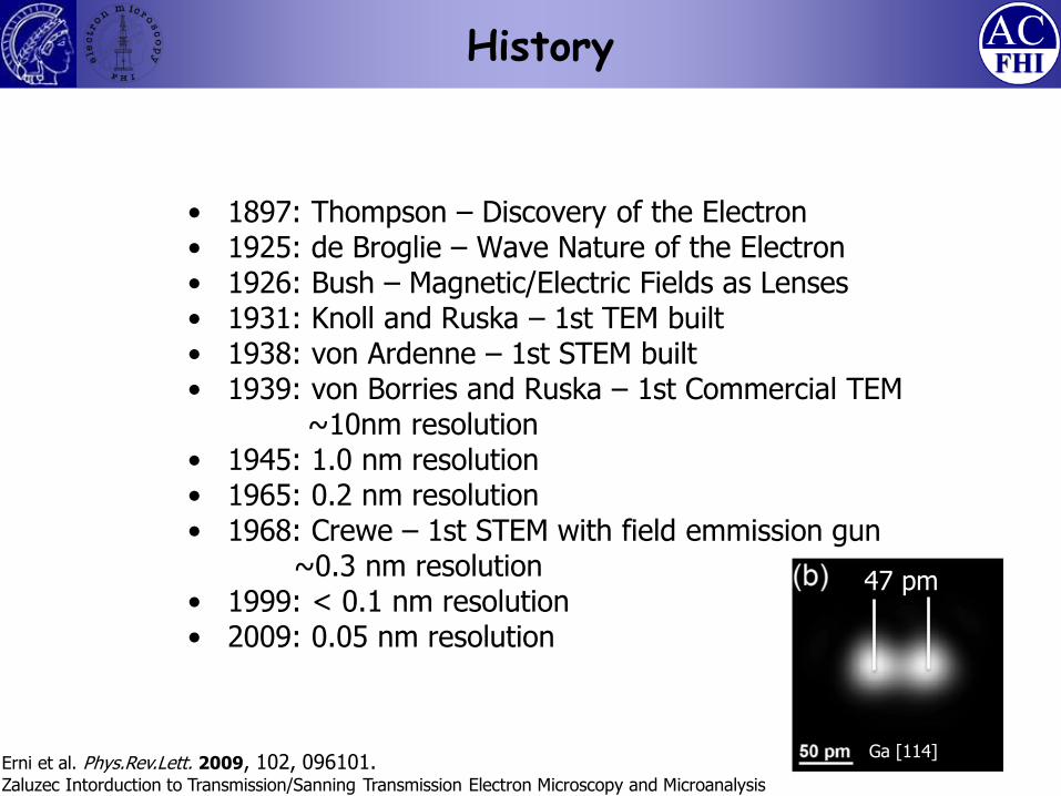
• 1897: Thompson – Discovery of the Electron • 1925: de Broglie – Wave Nature of the Electron • 1926: Bush – Magnetic/Electric Fields as Lenses • 1931: Knoll and Ruska – 1st TEM built • 1938: von Ardenne – 1st STEM built • 1939: von Borries and Ruska – 1st Commercial TEM ~10nm resolution • 1945: 1.0 nm resolution • 1965: 0.2 nm resolution • 1968: Crewe – 1st STEM with field emmission gun ~0.3 nm resolution • 1999: < 0.1 nm resolution • 2009: 0.05 nm resolution
47 pm
Ga [114] Erni et al. Phys.Rev.Lett. 2009, 102, 096101. Zaluzec Intorduction to Transmission/Sanning Transmission Electron Microscopy and Microanalysis
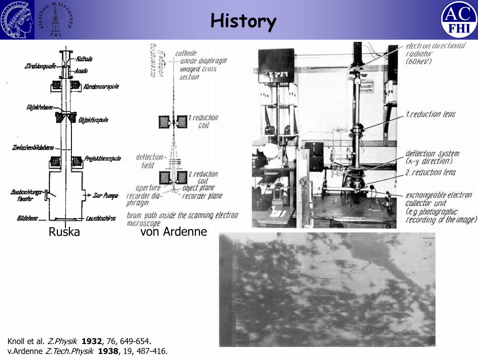
Ruska von Ardenne
Knoll et al. Z.Physik 1932, 76, 649-654. v.Ardenne Z.Tech.Physik 1938, 19, 4ß7-416.
History
Aim of the talk
• STEM is a very powerful and versatile instrument for atomic resolution imaging and nanoscale analysis
What is STEM?
What experiments can be done?
What are the principles of operation?
What are limiting factors in performance?
Outline
• Principles of STEM
• STEM Probe
• Ronchigram
• Detectors
• Incoherent vs. Coherent Imaging
• Examples
• Literature
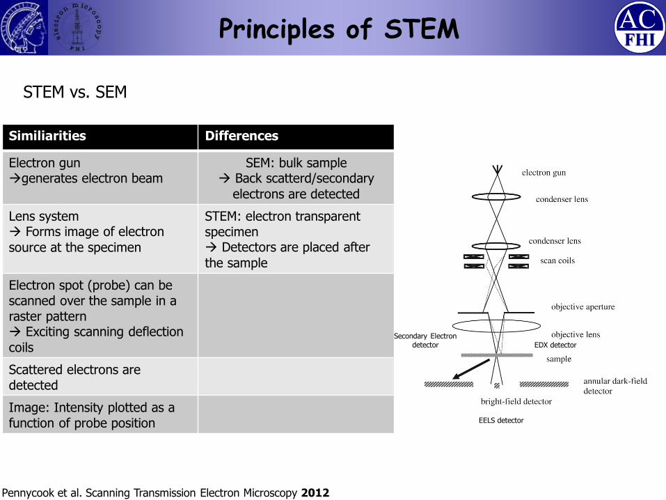
Principles of STEM
STEM vs. SEM
Similiarities Differences
Electron gun generates electron beam
SEM: bulk sample Back scatterd/secondary
electrons are detected
Lens system Forms image of electron
source at the specimen
STEM: electron transparent specimen Detectors are placed after
the sample
Electron spot (probe) can be scanned over the sample in a raster pattern Exciting scanning deflection
coils
Scattered electrons are detected
Image: Intensity plotted as a function of probe position
Secondary Electron detector EDX detector
EELS detector
Pennycook et al. Scanning Transmission Electron Microscopy 2012
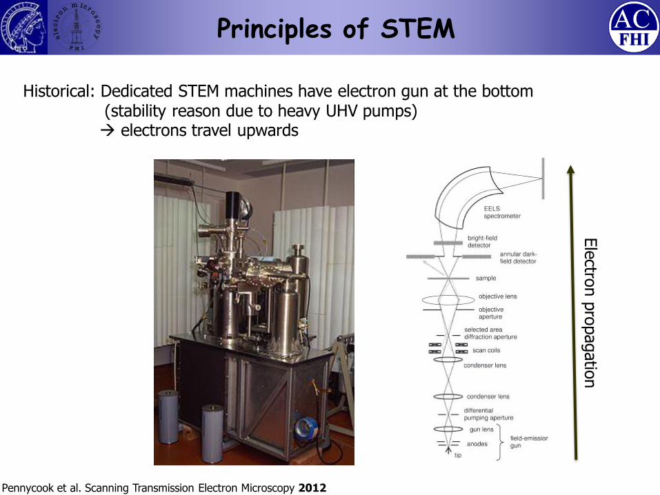
Principles of STEM
Historical: Dedicated STEM machines have electron gun at the bottom (stability reason due to heavy UHV pumps) electrons travel upwards
Ele
ctron p
ropagatio
n
Pennycook et al. Scanning Transmission Electron Microscopy 2012
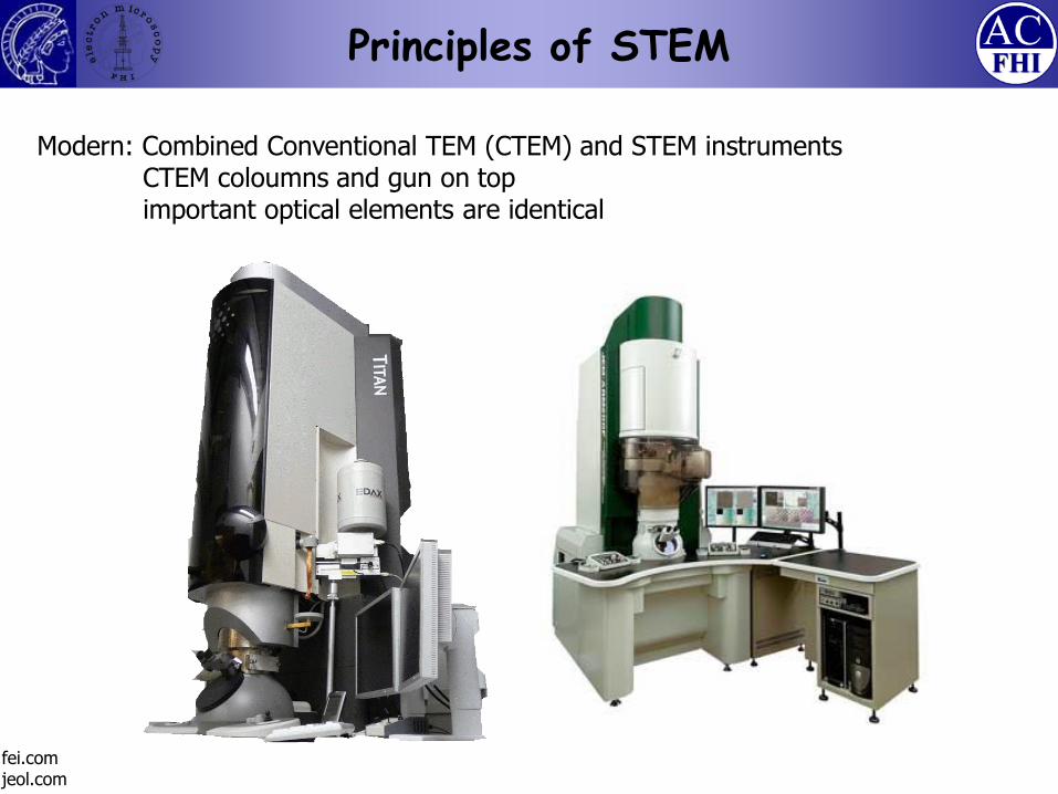
Principles of STEM
Modern: Combined Conventional TEM (CTEM) and STEM instruments CTEM coloumns and gun on top important optical elements are identical
fei.com jeol.com
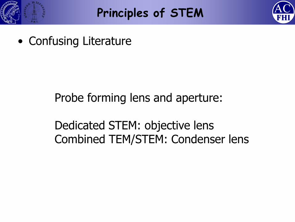
• Confusing Literature
Principles of STEM
Probe forming lens and aperture: Dedicated STEM: objective lens Combined TEM/STEM: Condenser lens
Principle of STEM
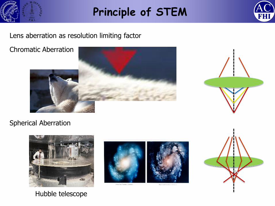
Lens aberration as resolution limiting factor Chromatic Aberration
Spherical Aberration
Hubble telescope
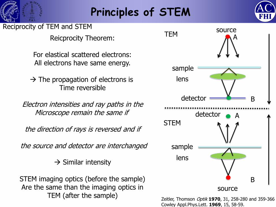
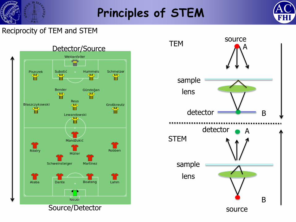
Principles of STEM Reciprocity of TEM and STEM
Condense
r le
ns
Cs = 0
Cs > 0
Phase difference (wave front error)
Reicprocity Theorem:
For elastical scattered electrons: All electrons have same energy.
The propagation of electrons is
Time reversible
Electron intensities and ray paths in the Microscope remain the same if
the direction of rays is reversed and if
the source and detector are interchanged
Similar intensity
STEM imaging optics (before the sample) Are the same than the imaging optics in
TEM (after the sample) Zeitler, Thomson Optik 1970, 31, 258-280 and 359-366 Cowley Appl.Phys.Lett. 1969, 15, 58-59.
source
sample
lens
detector
detector
source
lens
sample
B
A
A
B
TEM
STEM
Principles of STEM
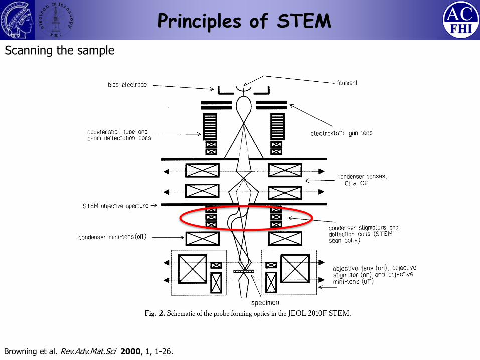
Scanning the sample
Browning et al. Rev.Adv.Mat.Sci 2000, 1, 1-26.
Principles of STEM
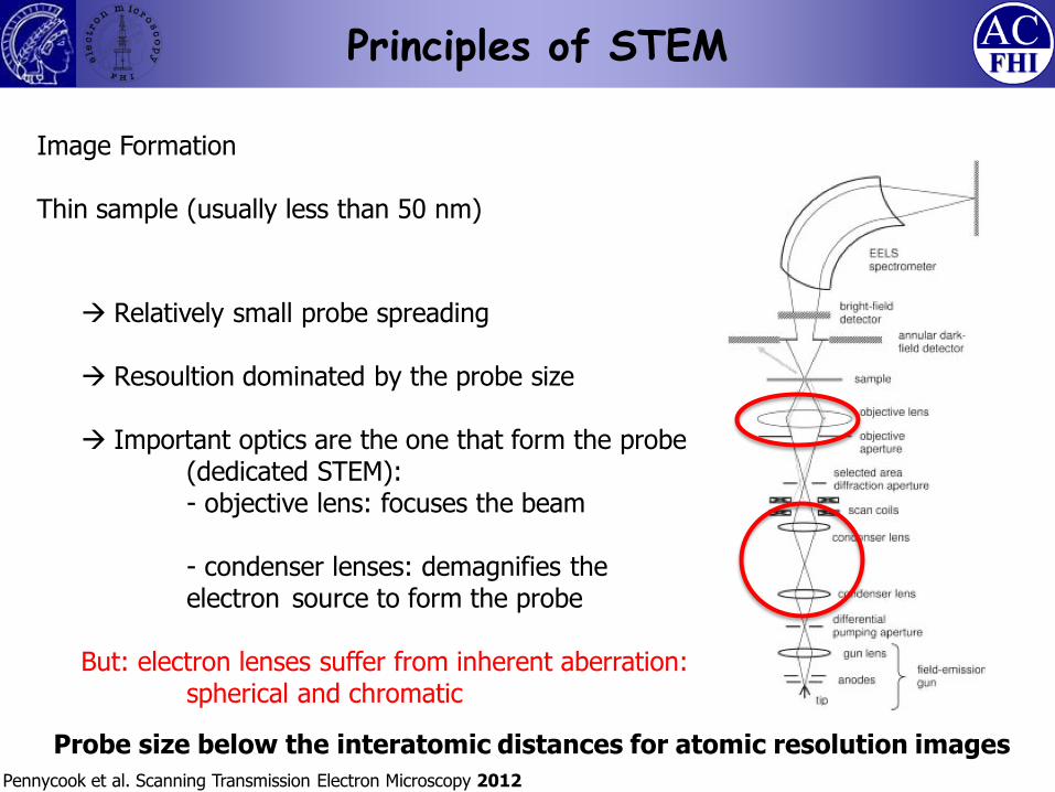
Image Formation Thin sample (usually less than 50 nm)
Relatively small probe spreading
Resoultion dominated by the probe size
Important optics are the one that form the probe (dedicated STEM): - objective lens: focuses the beam - condenser lenses: demagnifies the electron source to form the probe But: electron lenses suffer from inherent aberration: spherical and chromatic
Probe size below the interatomic distances for atomic resolution images
Pennycook et al. Scanning Transmission Electron Microscopy 2012
Principles of STEM
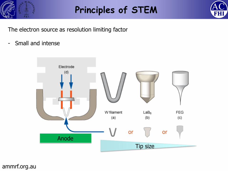
The electron source as resolution limiting factor - Small and intense
ammrf.org.au
Tip size
Anode
Principles of STEM
A field emission gun is based on a release of electrons from surface of sharply pointed tungsten tip
as a result of application of a strong electric field(>107 Vm-1).
The field emission is caused by applying a voltage
between the tip and an aperture metal anode.
Higher brightness is achieved from the gun that consists of two electrodes:
the first electrode has the extraction voltage and the second one has the final accelerating voltage,
required for the electron gun. There are two types of field emission gun differ mainly by their tips:
•CFE - cold field emitter is the base type. Application of the very strong electric field causes the surface energy barrier
to deform to such an extent that it becomes physically very narrow. There becomes a finite probability of electrons from the
•Fermi level penetrating the barrier even at ambient temperature. Usually made of single crystal tungsten sharpened tip with radius of about 100 nm,
• the needle is so sharp that electrons are extracted directly from the tip.
•SE – Schottky emitter. The Schottky emitter combines the high brightness and low energy spread of the cold field emitter wit
•h the high stability and low beam noise of thermal emitters.
• A commercial Schottky emitting cathode is less sharp than the others; there a monatomic layer of ZrO is formed on the tungsten surface.
•This coating reduces the work function of the tungsten from 4.54 to 2.8 eV. At an operating temperature of about 1800 K, this emitter may
• not be as bright as the cold field emitter but it delivers stable high currents and is less demanding in operation.
The follow table summarizes the properties of common sources:
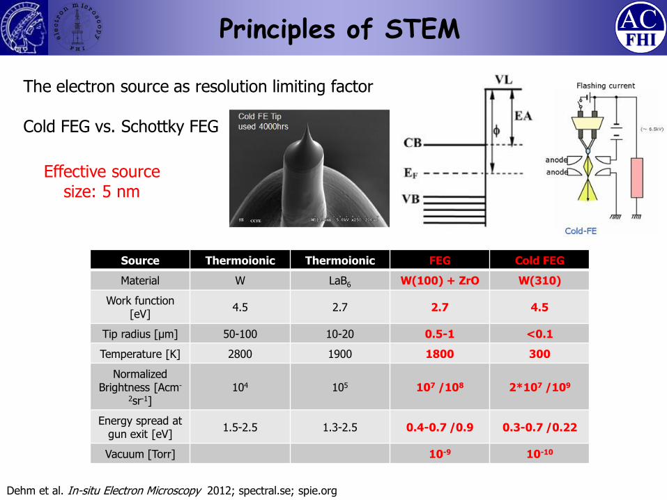
The electron source as resolution limiting factor Cold FEG vs. Schottky FEG
Dehm et al. In-situ Electron Microscopy 2012; spectral.se; spie.org
Source Thermoionic Thermoionic FEG Cold FEG
Material W LaB6 W(100) + ZrO W(310)
Work function [eV]
4.5 2.7 2.7 4.5
Tip radius [µm] 50-100 10-20 0.5-1 <0.1
Temperature [K] 2800 1900 1800 300
Normalized Brightness [Acm-
2sr-1] 104 105 107 /108 2*107 /109
Energy spread at gun exit [eV]
1.5-2.5 1.3-2.5 0.4-0.7 /0.9 0.3-0.7 /0.22
Vacuum [Torr] 10-9 10-10
Effective source size: 5 nm
Principles of STEM
Reciprocity of TEM and STEM
Condense
r le
ns
Cs = 0
Cs > 0
Phase difference (wave front error)
Source/Detector
Detector/Source
source
sample
lens
detector
detector
source
lens
sample
B
A
A
B
TEM
STEM
Outline
• Principles of STEM
• STEM Probe
• Ronchigram
• Detectors
• Incoherent vs. Coherent Imaging
• Examples
• Literature
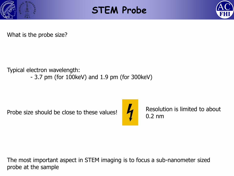
STEM Probe
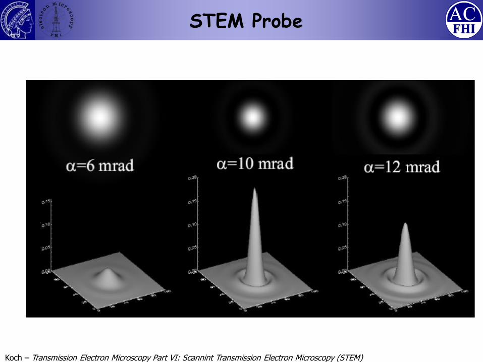
What is the probe size? Typical electron wavelength: - 3.7 pm (for 100keV) and 1.9 pm (for 300keV) Probe size should be close to these values!
Resolution is limited to about 0.2 nm
The most important aspect in STEM imaging is to focus a sub-nanometer sized probe at the sample
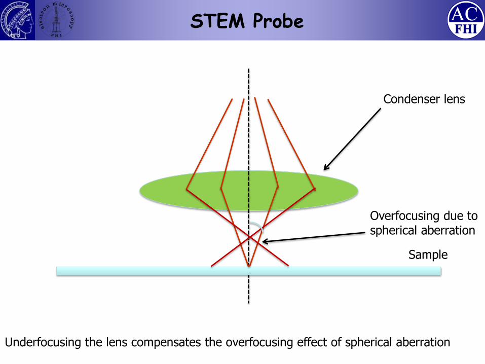
STEM Probe
Condenser lens
Sample
Overfocusing due to spherical aberration
Underfocusing the lens compensates the overfocusing effect of spherical aberration
Condenser lens
Condenser aperture
Sample
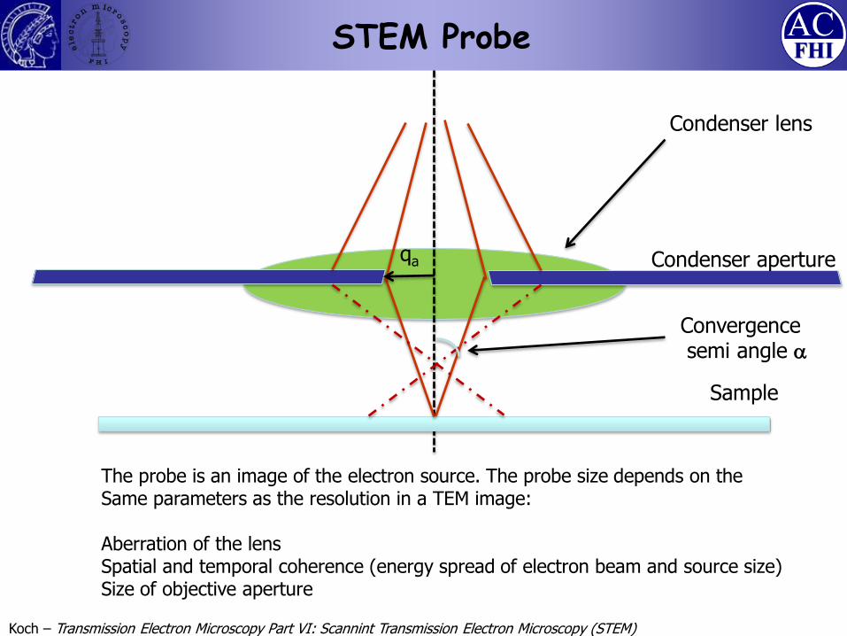
STEM Probe
Convergence semi angle
qa
The probe is an image of the electron source. The probe size depends on the Same parameters as the resolution in a TEM image: Aberration of the lens Spatial and temporal coherence (energy spread of electron beam and source size) Size of objective aperture
Koch – Transmission Electron Microscopy Part VI: Scannint Transmission Electron Microscopy (STEM)
𝜒 𝐾 = 𝜋𝑧𝜆 𝐾 ² +1
2𝜋𝐶𝑠𝜆³ 𝐾 4
𝐾 = 𝜃𝜆
Angle of convergence at the sample
Reciprocal space wave vector
phase shift
aperture function
𝐴 𝐾 = 𝐻
aberration funtion
wave function of incident electron porbe
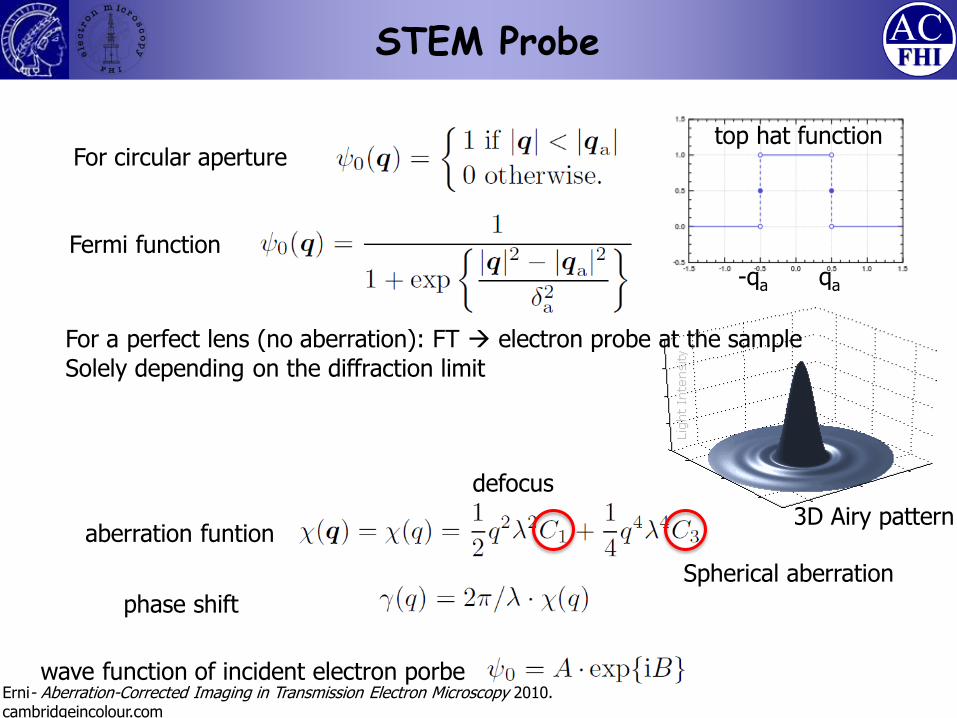
For circular aperture
Fermi function
top hat function
-qa qa
For a perfect lens (no aberration): FT electron probe at the sample
Solely depending on the diffraction limit
3D Airy pattern
defocus
Spherical aberration
STEM Probe
Erni- Aberration-Corrected Imaging in Transmission Electron Microscopy 2010. cambridgeincolour.com
𝜒 𝐾 = 𝜋𝑧𝜆 𝐾 ² +1
2𝜋𝐶𝑠𝜆³ 𝐾 4
𝐾 = 𝜃𝜆
Angle of convergence at the sample
Reciprocal space wave vector
aperture function
𝐴 𝐾 = 𝐻
STEM Probe
Condense
r le
ns
Cs = 0
Cs > 0
Phase difference (wave front error)
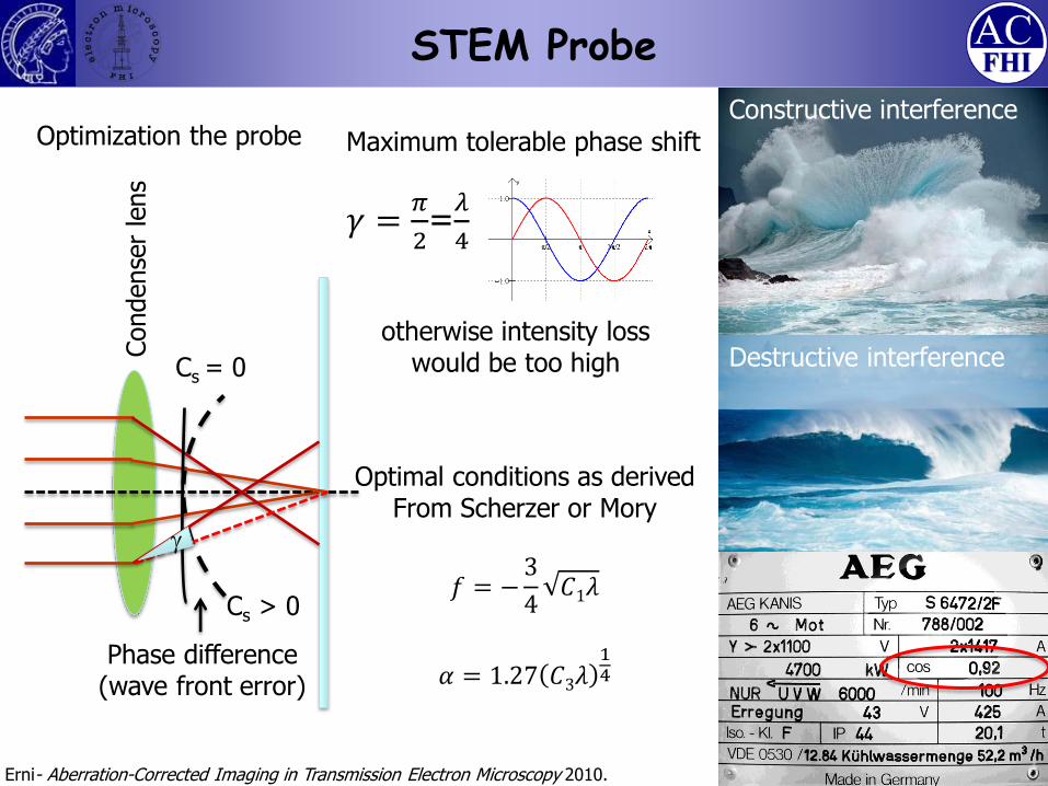
Maximum tolerable phase shift
𝛾 =𝜋
2=𝜆
4
otherwise intensity loss would be too high
Constructive interference
Destructive interference
Optimization the probe
Optimal conditions as derived From Scherzer or Mory
𝑓 = −3
4𝐶1𝜆
𝛼 = 1.27 𝐶3𝜆14
Erni- Aberration-Corrected Imaging in Transmission Electron Microscopy 2010.
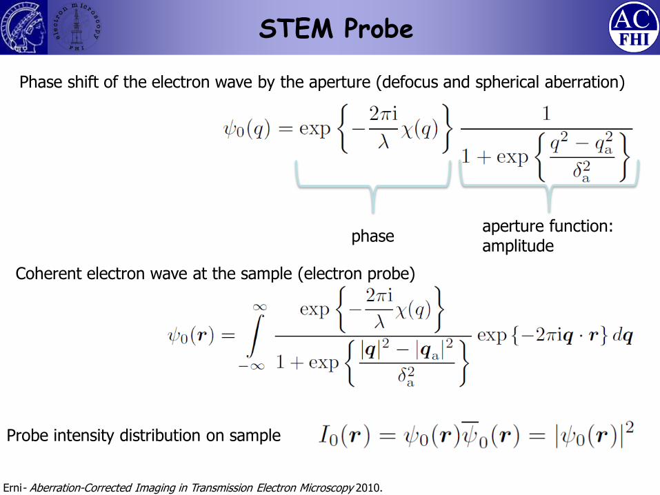
Probe intensity distribution on sample
Coherent electron wave at the sample (electron probe)
Phase shift of the electron wave by the aperture (defocus and spherical aberration)
phase aperture function: amplitude
STEM Probe
Erni- Aberration-Corrected Imaging in Transmission Electron Microscopy 2010.
STEM Probe
Koch – Transmission Electron Microscopy Part VI: Scannint Transmission Electron Microscopy (STEM)
STEM Probe
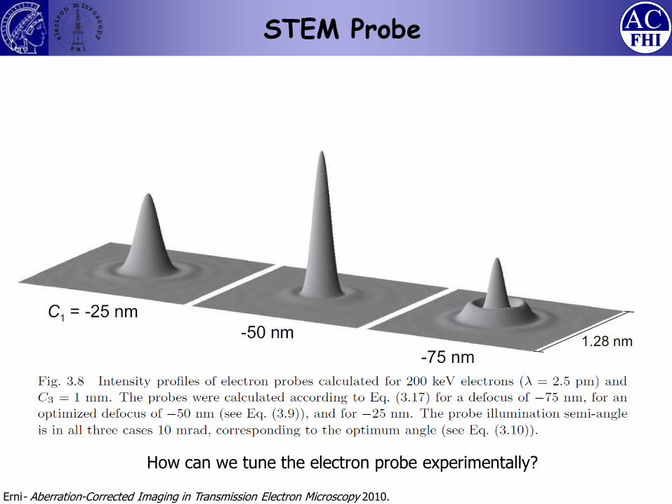
How can we tune the electron probe experimentally?
Erni- Aberration-Corrected Imaging in Transmission Electron Microscopy 2010.
Outline
• Principles of STEM
• STEM Probe
• Ronchigram
• Detectors
• Incoherent vs. Coherent Imaging
• Examples
• Literature
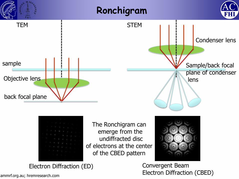
Ronchigram
Objective lens
back focal plane
sample Sample/back focal plane of condenser lens
Condenser lens
Convergent Beam Electron Diffraction (CBED)
Electron Diffraction (ED)
TEM STEM
The Ronchigram can emerge from the undiffracted disc
of electrons at the center of the CBED pattern
ammrf.org.au; hremresearch.com
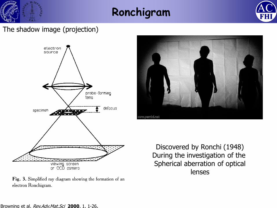
Ronchigram
The shadow image (projection)
Discovered by Ronchi (1948) During the investigation of the Spherical aberration of optical
lenses
Browning et al. Rev.Adv.Mat.Sci 2000, 1, 1-26.
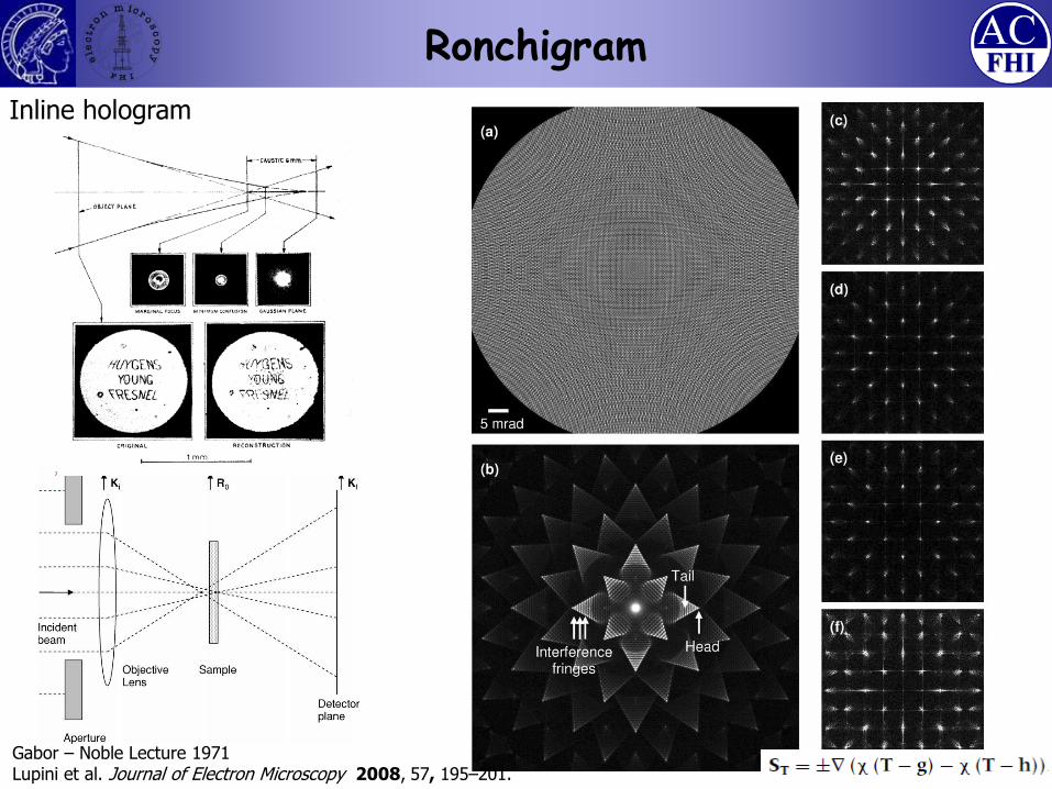
Ronchigram
Inline hologram
Gabor – Noble Lecture 1971 Lupini et al. Journal of Electron Microscopy 2008, 57, 195–201.
FHI
FHI
FHI
FHI
FHI
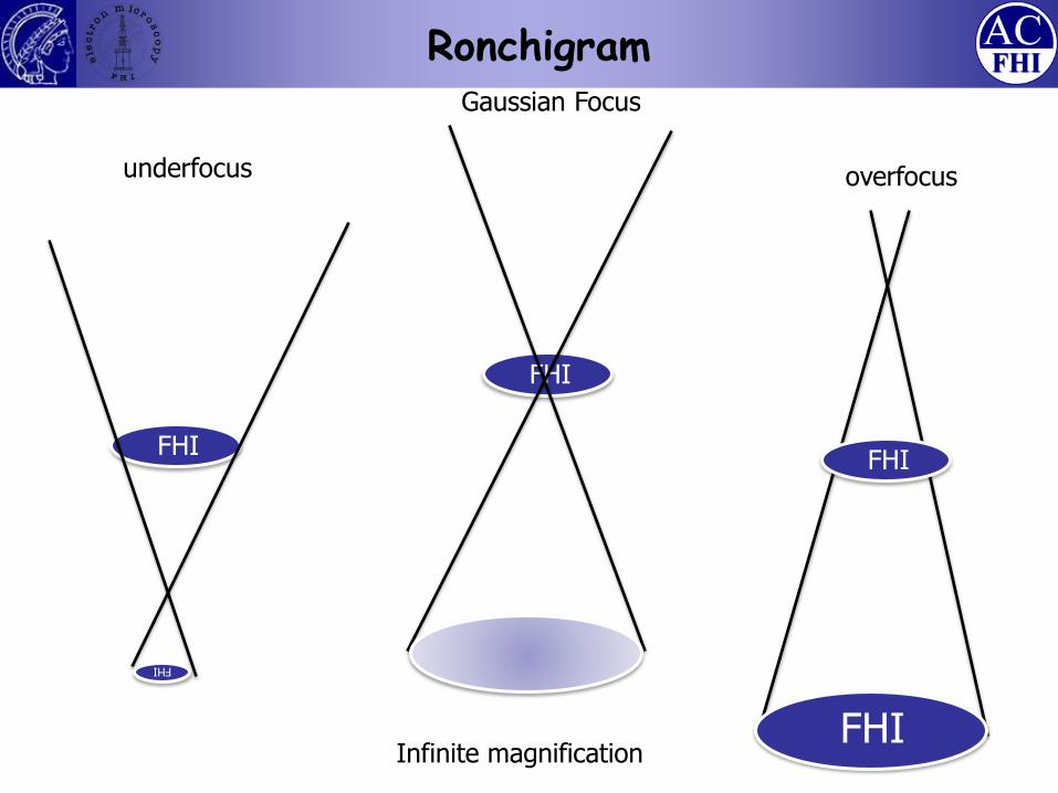
Gaussian Focus
underfocus overfocus
Ronchigram
Infinite magnification
Ronchigram
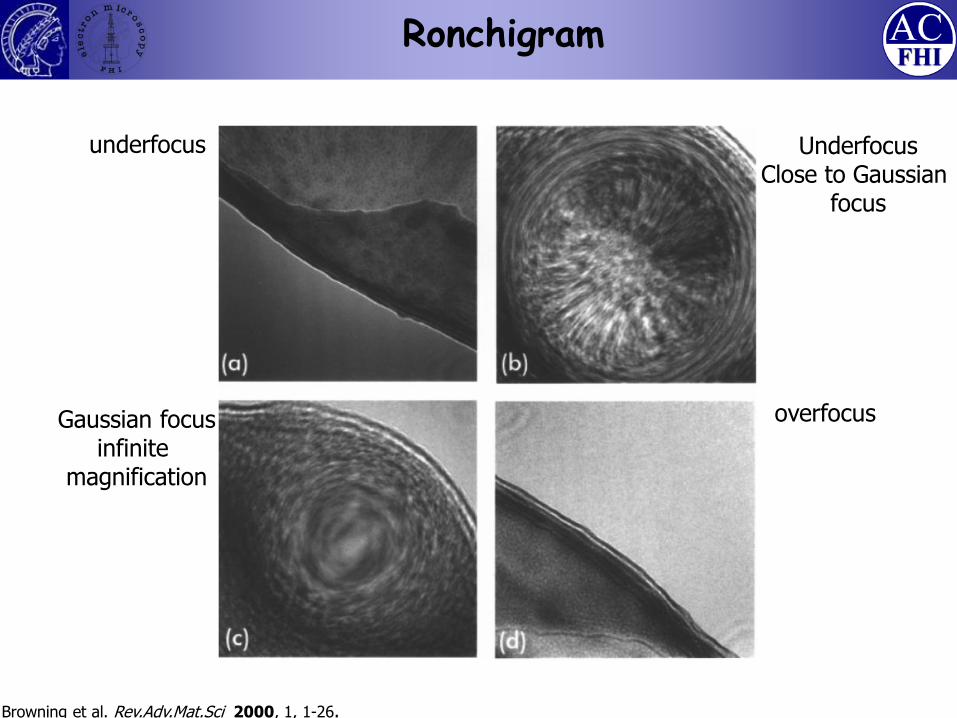
underfocus Underfocus Close to Gaussian
focus
overfocus Gaussian focus infinite
magnification
Browning et al. Rev.Adv.Mat.Sci 2000, 1, 1-26.
Ronchigram
Ek – A few concepts in TEM and STEM explained 2011.
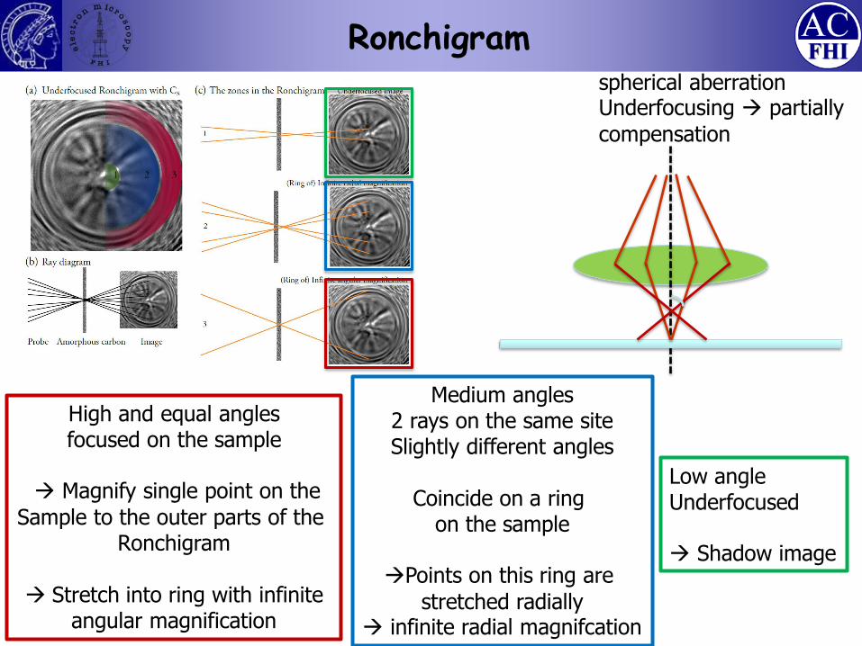
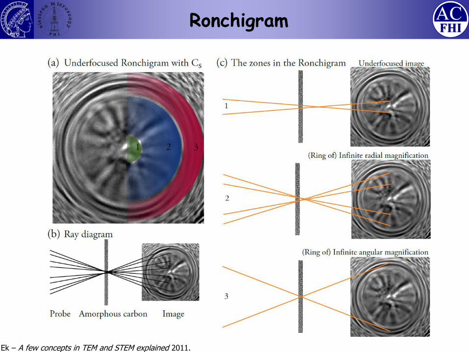
Ronchigram
High and equal angles focused on the sample
Magnify single point on the
Sample to the outer parts of the Ronchigram
Stretch into ring with infinite
angular magnification
spherical aberration Underfocusing partially
compensation
Medium angles 2 rays on the same site Slightly different angles
Coincide on a ring
on the sample
Points on this ring are
stretched radially infinite radial magnifcation
Low angle Underfocused Shadow image
Ronchigram
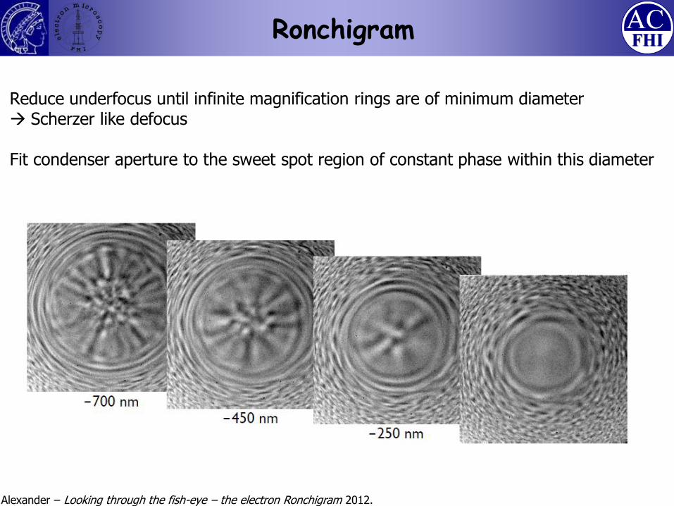
Reduce underfocus until infinite magnification rings are of minimum diameter Scherzer like defocus Fit condenser aperture to the sweet spot region of constant phase within this diameter
Alexander – Looking through the fish-eye – the electron Ronchigram 2012.
Ronchigram
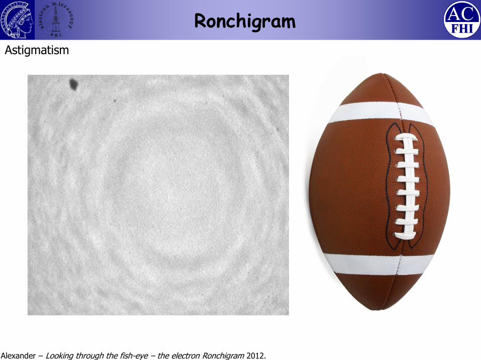
Astigmatism
Alexander – Looking through the fish-eye – the electron Ronchigram 2012.
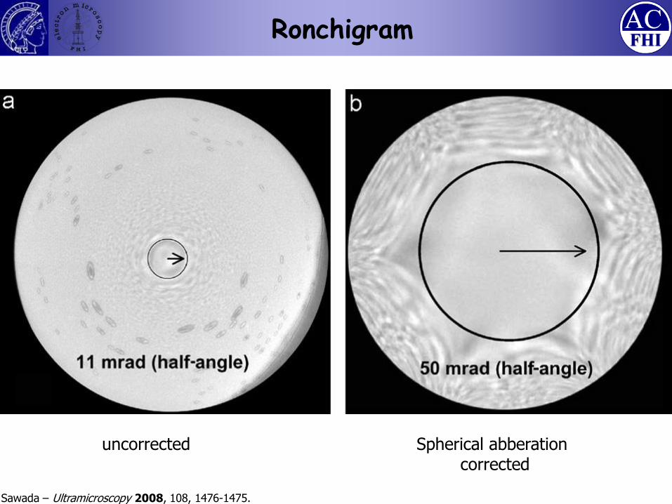
Ronchigram
uncorrected Spherical abberation corrected
Sawada – Ultramicroscopy 2008, 108, 1476-1475.
Outline
• Principles of STEM
• STEM Probe
• Ronchigram
• Detectors
• Incoherent vs. Coherent Imaging
• Examples
• Literature
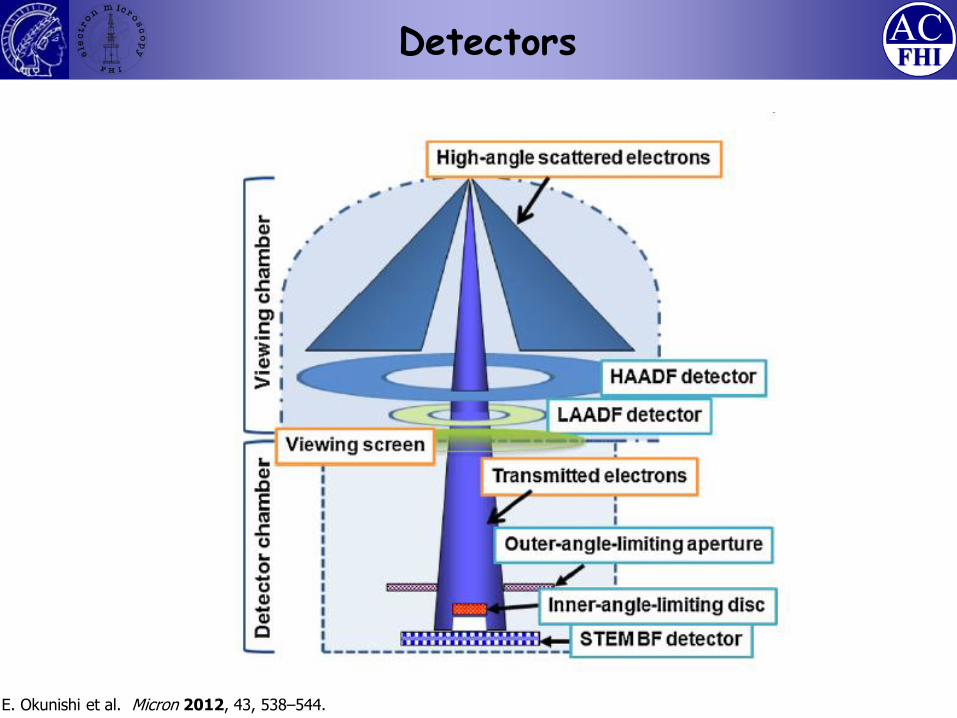
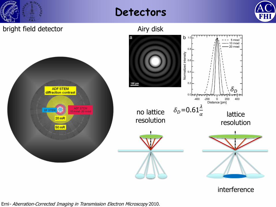
Detectors SE and EDX like in SEM Brightfield detector (BF): - disc - Scattering angles Centered on the optical axis Annular Dark Field (ADF):
- Annulus - Higher angle detects only scattered electrons - Unique to STEM - Incoherent images - Sensitive to atomic number Z
Detectors
E. Okunishi et al. Micron 2012, 43, 538–544.
Detectors
no lattice resolution
lattice resolution
interference
bright field detector
Erni- Aberration-Corrected Imaging in Transmission Electron Microscopy 2010.
𝛿𝐷
Airy disk
𝛿𝐷=0.61𝜆
𝛼
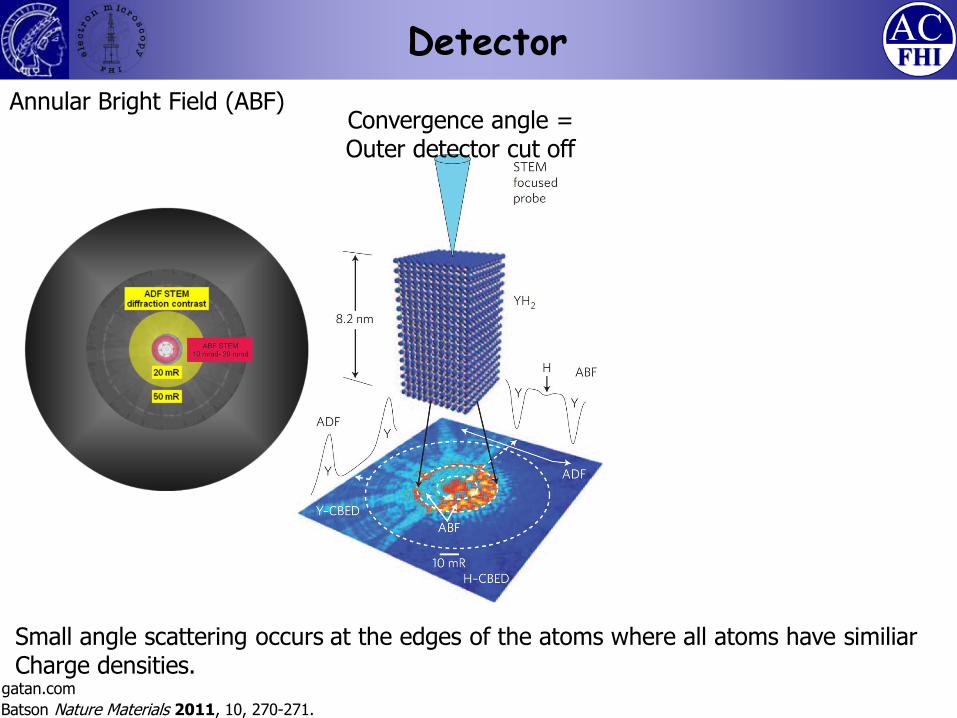
Detector
Small angle scattering occurs at the edges of the atoms where all atoms have similiar Charge densities.
Annular Bright Field (ABF) Convergence angle = Outer detector cut off
Batson Nature Materials 2011, 10, 270-271.
gatan.com
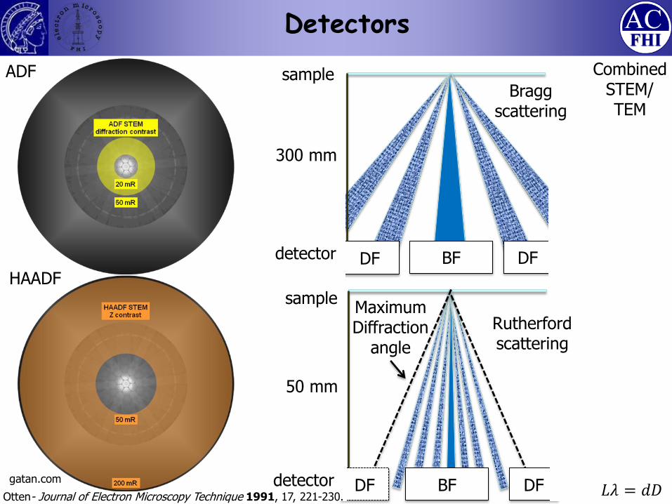
BF BF DF DF
Rutherford scattering
Maximum Diffraction
angle
Detectors
BF DF DF
300 mm
sample
detector
detector
sample
50 mm
Bragg scattering
𝐿𝜆 = 𝑑𝐷
Combined STEM/ TEM
ADF
HAADF
Otten- Journal of Electron Microscopy Technique 1991, 17, 221-230.
gatan.com
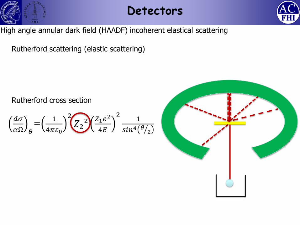
Detectors
Rutherford cross section
𝑑𝜎
𝛼Ω 𝜃=
1
4𝜋𝜀0
2𝑍2²
𝑍1𝑒2
4𝐸
21
𝑠𝑖𝑛4 𝜃2
Rutherford scattering (elastic scattering)
High angle annular dark field (HAADF) incoherent elastical scattering
Detectors
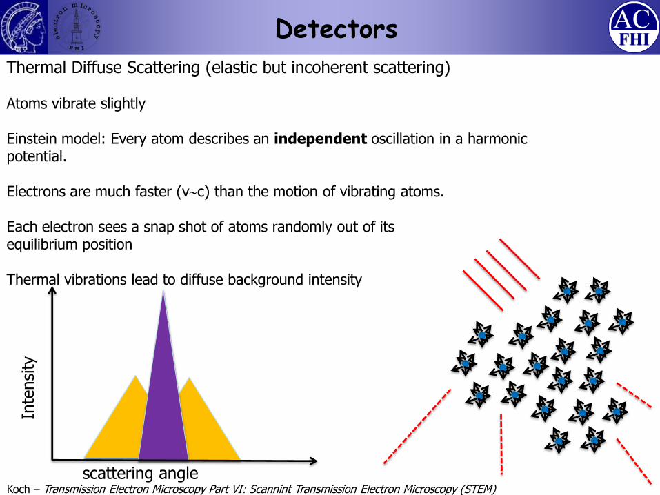
Thermal Diffuse Scattering (elastic but incoherent scattering) Atoms vibrate slightly Einstein model: Every atom describes an independent oscillation in a harmonic potential. Electrons are much faster (vc) than the motion of vibrating atoms. Each electron sees a snap shot of atoms randomly out of its equilibrium position Thermal vibrations lead to diffuse background intensity
scattering angle
Inte
nsi
ty
Koch – Transmission Electron Microscopy Part VI: Scannint Transmission Electron Microscopy (STEM)
Outline
• Principles of STEM
• STEM Probe
• Ronchigram
• Detectors
• Incoherent vs. Coherent Imaging
• Examples
• Literature
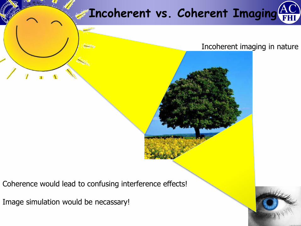
Incoherent vs. Coherent Imaging
Coherence would lead to confusing interference effects! Image simulation would be necassary!
Incoherent imaging in nature
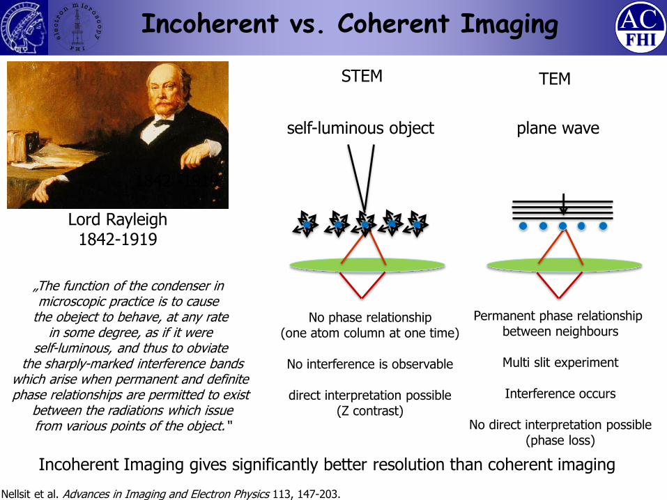
1842 -1919
Lord Rayleigh 1842-1919
„The function of the condenser in microscopic practice is to cause
the obeject to behave, at any rate in some degree, as if it were
self-luminous, and thus to obviate the sharply-marked interference bands
which arise when permanent and definite phase relationships are permitted to exist
between the radiations which issue from various points of the object.“
No phase relationship (one atom column at one time)
No interference is observable
direct interpretation possible
(Z contrast)
Permanent phase relationship between neighbours
Multi slit experiment
Interference occurs
No direct interpretation possible
(phase loss)
self-luminous object plane wave
Incoherent vs. Coherent Imaging
Incoherent Imaging gives significantly better resolution than coherent imaging
STEM TEM
Nellsit et al. Advances in Imaging and Electron Physics 113, 147-203.
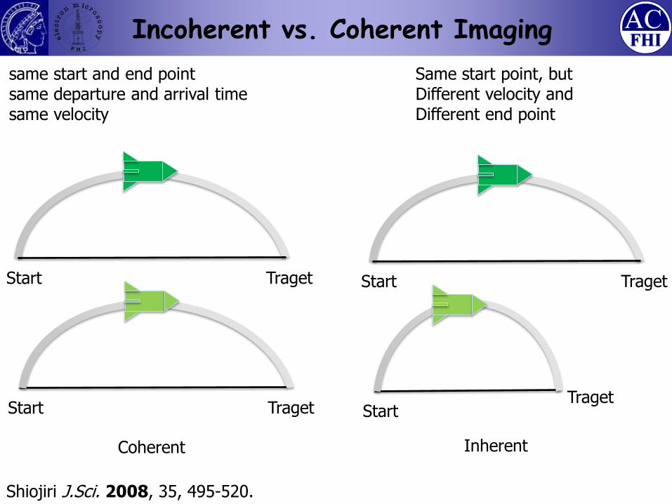
Incoherent vs. Coherent Imaging
Traget Start
Traget Start
same start and end point same departure and arrival time same velocity
Traget Start
Traget Start
Same start point, but Different velocity and Different end point
Coherent Inherent
Shiojiri J.Sci. 2008, 35, 495-520.
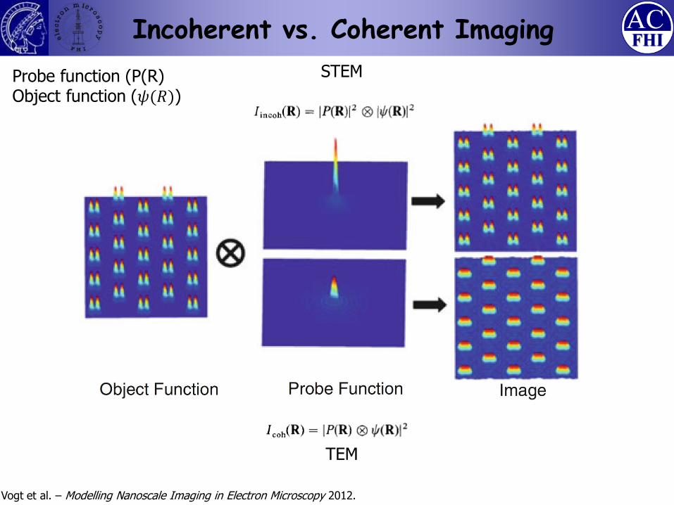
Incoherent vs. Coherent Imaging
TEM
STEM Probe function (P(R) Object function (𝜓(𝑅))
Vogt et al. – Modelling Nanoscale Imaging in Electron Microscopy 2012.
Outline
• Principles of STEM
• STEM Probe
• Ronchigram
• Detectors
• Incoherent vs. Coherent Imaging
• Examples
• Literature
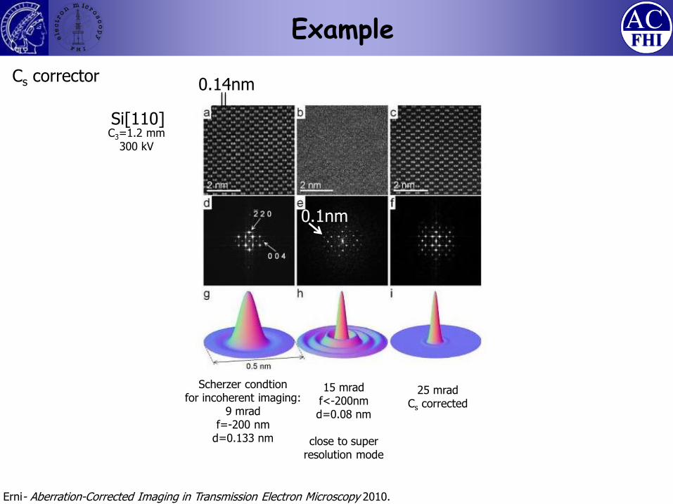
Example
15 mrad f<-200nm d=0.08 nm
close to super
resolution mode
25 mrad Cs corrected
Si[110]
Scherzer condtion for incoherent imaging:
9 mrad f=-200 nm
d=0.133 nm
0.14nm
C3=1.2 mm 300 kV
0.1nm
Cs corrector
Erni- Aberration-Corrected Imaging in Transmission Electron Microscopy 2010.
Outline
• Principles of STEM
• STEM Probe
• Ronchigram
• Detectors
• Incoherent vs. Coherent Imaging
• Examples
• Literature
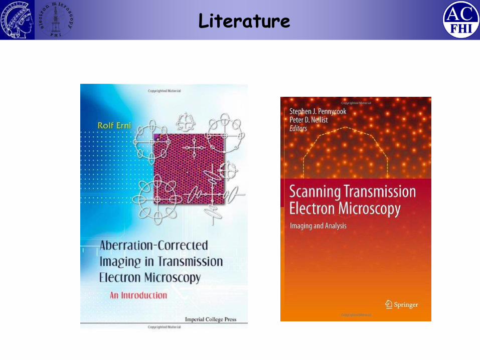
Literature
Thank you very much for your attention!!!


![Ultrafast transmission electron microscopy using a laser ...transmission electron microscopy [4], scanning electron microscopy [5], x-ray diffraction [6], scanning tunneling and atomic](https://img.dokumen.tips/doc/110x75/607eb1335ce8082131294459/ultrafast-transmission-electron-microscopy-using-a-laser-transmission-electron.jpg)