Embed Size (px)
Citation preview
Scanning ultrafast electron microscopyDing-Shyue Yang, Omar F. Mohammed, and Ahmed H. Zewail1
Physical Biology Center for Ultrafast Science and Technology, Arthur Amos Noyes Laboratory of Chemical Physics, California Institute of Technology,Pasadena, CA 91125
Contributed by Ahmed H. Zewail, June 29, 2010 (sent for review June 1, 2010)
Progress has been made in the development of four-dimensionalultrafast electron microscopy, which enables space-time imagingof structural dynamics in the condensed phase. In ultrafast electronmicroscopy, the electrons are accelerated, typically to 200 keV, andthe microscope operates in the transmission mode. Here, we reportthe development of scanning ultrafast electron microscopy using afield-emission-source configuration. Scanning of pulses is made inthe single-electron mode, for which the pulse contains at most oneor a few electrons, thus achieving imaging without the space-charge effect between electrons, and still in ten(s) of seconds.For imaging, the secondary electrons from surface structures aredetected, as demonstrated here for material surfaces and biologi-cal specimens. By recording backscattered electrons, diffractionpatterns from single crystals were also obtained. Scanning pulsed-electron microscopy with the acquired spatiotemporal resolutions,and its efficient heat-dissipation feature, is now poised to providein situ 4D imaging and with environmental capability.
biological imaging ∣ Schottky emission source ∣ structural dynamics ∣nanomaterials imaging
The development of ultrafast electron microscopy (UEM) hasenabled imaging in both space and time with atomic-scale
resolutions (1, 2). The central concept involved is that of single-electron packets, which provide the high spatiotemporal resolu-tions due to the absence of the space-charge effect between elec-trons. Using femtosecond (fs) optical pulses, the electrons aregenerated from a LaB6 photocathode and then acceleratedtypically to 200 keV. The time resolution is independent of the re-sponse of the video camera, as it is determined by the duration ofthe initial heating and electron pulses. With UEM, the differentdomains of electron microscopy were made possible: real-spaceimaging (3–5), diffraction (6–8), and electron-energy-loss spectro-scopy (9, 10). Recent advances include 4D electron tomography(11), convergent-beam diffraction (12), and near-field electronmicroscopy (13).
SEM provides the unique capability of obtaining 3D-likeimages for materials surfaces (14–16). Moreover, environmentalmicroscopy (17) can easily be invoked. Significantly, the electronsource in SEM, a field emitter with a tip dimension of tens-to-hundreds of nanometers (nm), has higher brightness than thatof the source in UEM (LaB6), which has an active-area dimen-sion of tens of micrometers (μm). Finally, the specimen is easierto handle; thick samples can be used and provide the means forheat dissipation, especially when the heating pulse is involved indynamical studies.
Introducing ultrashort time resolution in SEMwas not possiblebefore, as in the past time-resolved studies were made by “chop-ping” the electron beam through the technique of high-frequency(MHz or GHz) beam deflection and blanking (18, 19). The tem-poral width of an electron pulse was hundreds of picoseconds (ps)and the overall resolution of the system was on the order of 10 na-noseconds (ns) (19). The main application of this methodologywas in the study of the response of microelectronic devices orcircuits under variation of the voltage applied; the vibrationalmechanics of microstructures under the influence of varying vol-tages was also examined (20). Recently, spectroscopic detectionof cathodoluminescence was resolved in the studies of carrier dy-
namics with 50 nm and 10 ps spatiotemporal resolutions (21, 22).For these studies, the electrons interacting with the specimenwere responsible for the luminescence that was detected by astreak camera.
The concept of scanning ultrafast electron microscopy(SUEM) is entirely different in that the spatial resolution is thatof SEM and the time resolution is determined by the ultrashortpulses involved, not by the deflection rate (19) or the streak cam-era used for optical detection (21). Unlike in the latter case wherethe electron pulse induces the carrier excitations, in SUEM, theelectron pulses are the probes for imaging through the resultantsecondary electrons. In this regard, the scheme of pump-probe issimilar to that used in UEM (1) but with a different detectionmechanism, a pixel-by-pixel recording rather than parallel pro-cessing of the image. Some key differences, however, do exist.Besides the scanning mode of operation, the observed signalsin SUEM are obtained in the form of secondary or backscatteredelectrons, which are mainly the result of inelastic scattering.
Another difference is in the observed diffraction. Bragg spotsor Debye–Scherrer rings, which are the dominant features ofUEM diffraction, are replaced by Kikuchi lines (15, 23) whenelectron backscattering diffraction (EBSD) patterns are recordedin SUEM. As such, they are useful in resolving the structuralevolution in a crystalline grain or domain along different crystal-lographic directions. Lastly, from a technical point of view, ourcurrent SUEM has a zirconium-oxide-coated sharp tungstentip, which is a Schottky-emission gun in the relatively low-fluenceregime (reaching field emission in the high-fluence limit) that isdifferent from the LaB6 tips used in the first and second genera-tions (UEM1 and UEM2) in this laboratory. When operated inthe conventional continuous emission mode (hereafter referredto as the SEM mode), these field-emission sources are known tobe orders of magnitude higher in brightness (1011–1012 A∕m2∕sr)than LaB6 (15). Thus, the advance in ultrafast imaging is signifi-cant for the further improvement of the source’s coherencewidth (1).
Here, we report the first results obtained in SUEM. The sourceemitter is side-illuminated by a focused fs pulse of well-definedpolarization, and the photoemitted electron pulse is the probe inimaging and diffraction recordings. Applications are demon-strated for biological and nanostructured materials over a widerange of magnification. Using the pulsed electrons in SUEM,diffraction patterns, obtained by detecting the backscatteredelectrons, were also recorded for a silicon wafer, and indeedthe patterns display the Kikuchi lines. From these initial results,we expect the technique to open up various applications, as inUEM, but with the additional capability of scanning surfacesand the environmental microscopy mode.
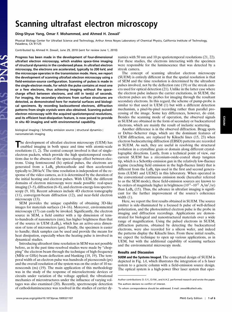
Results and DiscussionSUEM and the Systems Imaged. The conceptual design of SUEM isdepicted in Fig. 1A, which illustrates the integration of a fs lasersystem to a generic column with a field-emission source design.The optical system is a high-power fiber laser system that oper-
Author contributions: D.-S.Y., O.F.M., and A.H.Z. performed research and wrote the paper.
The authors declare no conflict of interest.1To whom correspondence should be addressed. E-mail: [email protected].
www.pnas.org/cgi/doi/10.1073/pnas.1009321107 PNAS Early Edition ∣ 1 of 6
PHYS
ICS
ates at variable repetition rates, from 200 kHz to 25.2 MHz. Thelaser delivers fs infrared pulses with an average power of up to∼20 W; the wavelength is centered at 1030 nm and the pulsewidth is less than 300 fs. This infrared output is frequencydoubled and tripled (or quadrupled) in a set of two nonlinearβ-BaB2O4 crystals: the 515 nm pulses could be used in dynamicsinitiation in the specimen, whereas the 343 nm (or 257 nm) pulsesare used for the generation of the electron pulse train. The ultra-violet light is separated and directed by dichroic mirrors, andtightly focused by a 125 mm focal lens onto the tip of the electronemitter (see below). At 25.2 MHz, the average pulse energy of theultraviolet beam reaches ∼2 nJ, before entering the microscope,resulting in an energy density of Flaser ∼ 1 mJ∕cm2 at the emit-ter tip.
The basic scanning mechanism of SEM was utilized with theelectron acceleration voltage of up to 30 kV. As mentionedearlier, the cathode is a zirconium-oxide-coated tungsten ½ZrOx∕Wð100Þ� tip of several hundred nm in diameter. The work func-tion is lowered by the ZrOx coating from 4.5 eV to ∼2.8 eV athigh temperatures (16, 24–26). In the presence of an electrostaticfield of jEDCj ∼ 107 V∕cm, the effective work function is furtherlowered by ∼1.2 eV to ϕeff ∼ 1.6 eV (i.e., the Schottky effect); seebelow. Thus in this extended Schottky (thermionic, field-emission) regime (24, 25), electrons at a temperature of 1800 K(filament current of 2.48 A) can overcome the barrier, with somecontribution from the tunneling effect, which is dominant inthe field-emission regime for which the potential barrier widthis considerably reduced.
In the SUEM mode, the filament current is completely turnedoff to suppress the background emission from the source at ele-vated temperatures. In the original design of the electron column,a pyrometrical window was introduced for viewing the glowing
emitter and measuring its temperature remotely. The same win-dow becomes a convenient entry port for the light pulses, definingthe configuration of side-illumination of the emitter (Fig. 1B). Atroom temperature, the work function of the ZrOx∕Wð100Þ tip isbelieved to be different and may be as high as that of tungsten inthe absence of EDC (27). As a result, the photon energy is higherthan the work function of the cold emitter (lowered by ∼1.2 eVdue to the Schottky effect) by a small fraction (∼0.3) of an eV forthe 343 nm excitation. Therefore, electrons overcome this energybarrier through the absorption of the ultrafast photons, and notby the thermal effect, as demonstrated below.
Polarization of the ultraviolet beam is adjusted relative to thetip axis through a half-wave plate to maximize the pulsed current.The photoelectron trajectories follow the pathways that are de-fined by the components of the electron optics, and, as in SEM,they are the condenser lenses, stigmator, scan coils and the ob-jective lens (Fig. 1A). After exiting the polepiece and entering thespecimen chamber, the focused pulsed electron beam is directedby the scan coils and rasters across a specified region of the speci-men to form an image (Fig. 1C).
The image construction is achieved through the scanningprocess with a well-defined dwell time for each beam location.It is the result of mapping over discrete pixels in the informationspace, thus forming a one-to-one correspondence with the set ofbeam locations on the specimen. The electron-matter interactionresults in various types of signals, such as secondary and backscat-tered electrons as well as X-rays, and these are recorded by dif-ferent detectors (15, 16). Here, we present secondary-electronimages obtained by a positively biased Everhart–Thornley detec-tor, and EBSD patterns recorded by a high-sensitivity digitalcamera.
Fig. 1. Scanning ultrafast electron microscopy (SUEM), a conceptual schematic. (A) The interface of a femtosecond laser system to a modified SEM. (B) A close-up view of the field-emission region. Side-illumination of the field emitter by fs ultraviolet pulses is used for the electron generation. (C) A close-up view of theprobe region and schematic for the pixel-by-pixel image construction. The axis of time is introduced by adjusting the arrival time of the laser excitation pulse atthe specimen relative to that of the electron probe pulse using a variable optical delay line.
2 of 6 ∣ www.pnas.org/cgi/doi/10.1073/pnas.1009321107 Yang et al.
To initiate a dynamical change in the specimen, as in UEM(1, 2), a clocking pulse must be introduced. In SUEM, a secondwindow was included to permit the entry of such pulses into thechamber, and an optical delay stage was used for the control ofthe arrival times of the initiating and electron pulses at the speci-men (Fig. 1A). For the first set of studies reported here, we focuson the feasibility of obtaining such images and diffraction pat-terns, and in future work we will address the time dependencein a similar manner to that of UEM.
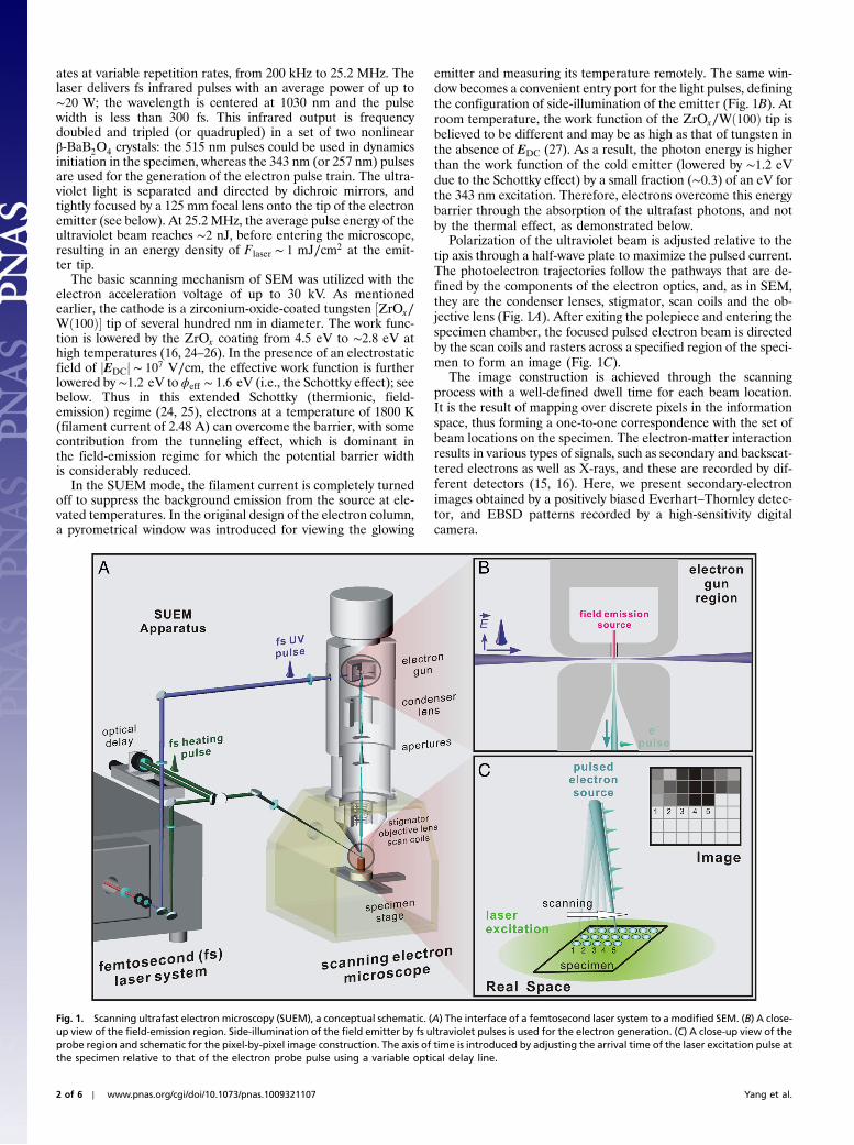
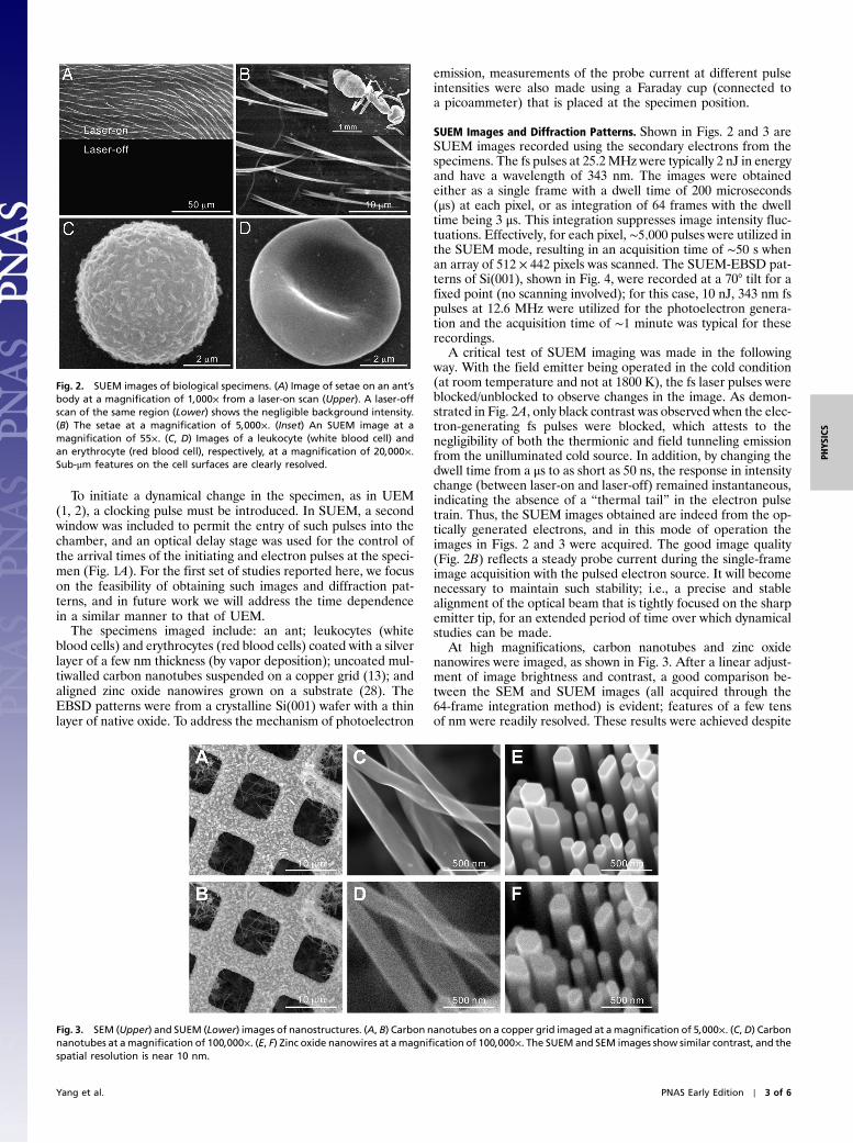
The specimens imaged include: an ant; leukocytes (whiteblood cells) and erythrocytes (red blood cells) coated with a silverlayer of a few nm thickness (by vapor deposition); uncoated mul-tiwalled carbon nanotubes suspended on a copper grid (13); andaligned zinc oxide nanowires grown on a substrate (28). TheEBSD patterns were from a crystalline Si(001) wafer with a thinlayer of native oxide. To address the mechanism of photoelectron
emission, measurements of the probe current at different pulseintensities were also made using a Faraday cup (connected toa picoammeter) that is placed at the specimen position.
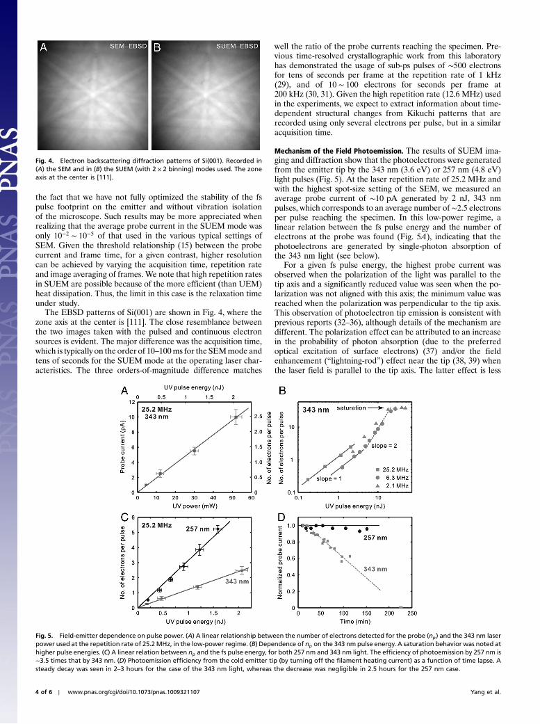
SUEM Images and Diffraction Patterns. Shown in Figs. 2 and 3 areSUEM images recorded using the secondary electrons from thespecimens. The fs pulses at 25.2MHz were typically 2 nJ in energyand have a wavelength of 343 nm. The images were obtainedeither as a single frame with a dwell time of 200 microseconds(μs) at each pixel, or as integration of 64 frames with the dwelltime being 3 μs. This integration suppresses image intensity fluc-tuations. Effectively, for each pixel, ∼5;000 pulses were utilized inthe SUEM mode, resulting in an acquisition time of ∼50 s whenan array of 512 × 442 pixels was scanned. The SUEM-EBSD pat-terns of Si(001), shown in Fig. 4, were recorded at a 70° tilt for afixed point (no scanning involved); for this case, 10 nJ, 343 nm fspulses at 12.6 MHz were utilized for the photoelectron genera-tion and the acquisition time of ∼1 minute was typical for theserecordings.
A critical test of SUEM imaging was made in the followingway. With the field emitter being operated in the cold condition(at room temperature and not at 1800 K), the fs laser pulses wereblocked/unblocked to observe changes in the image. As demon-strated in Fig. 2A, only black contrast was observed when the elec-tron-generating fs pulses were blocked, which attests to thenegligibility of both the thermionic and field tunneling emissionfrom the unilluminated cold source. In addition, by changing thedwell time from a μs to as short as 50 ns, the response in intensitychange (between laser-on and laser-off) remained instantaneous,indicating the absence of a “thermal tail” in the electron pulsetrain. Thus, the SUEM images obtained are indeed from the op-tically generated electrons, and in this mode of operation theimages in Figs. 2 and 3 were acquired. The good image quality(Fig. 2B) reflects a steady probe current during the single-frameimage acquisition with the pulsed electron source. It will becomenecessary to maintain such stability; i.e., a precise and stablealignment of the optical beam that is tightly focused on the sharpemitter tip, for an extended period of time over which dynamicalstudies can be made.
At high magnifications, carbon nanotubes and zinc oxidenanowires were imaged, as shown in Fig. 3. After a linear adjust-ment of image brightness and contrast, a good comparison be-tween the SEM and SUEM images (all acquired through the64-frame integration method) is evident; features of a few tensof nm were readily resolved. These results were achieved despite
Fig. 2. SUEM images of biological specimens. (A) Image of setae on an ant’sbody at a magnification of 1;000× from a laser-on scan (Upper). A laser-offscan of the same region (Lower) shows the negligible background intensity.(B) The setae at a magnification of 5;000×. (Inset) An SUEM image at amagnification of 55×. (C, D) Images of a leukocyte (white blood cell) andan erythrocyte (red blood cell), respectively, at a magnification of 20;000×.Sub-μm features on the cell surfaces are clearly resolved.
Fig. 3. SEM (Upper) and SUEM (Lower) images of nanostructures. (A, B) Carbon nanotubes on a copper grid imaged at amagnification of 5;000×. (C,D) Carbonnanotubes at amagnification of 100;000×. (E, F) Zinc oxide nanowires at amagnification of 100;000×. The SUEM and SEM images show similar contrast, and thespatial resolution is near 10 nm.
Yang et al. PNAS Early Edition ∣ 3 of 6
PHYS
ICS
the fact that we have not fully optimized the stability of the fspulse footprint on the emitter and without vibration isolationof the microscope. Such results may be more appreciated whenrealizing that the average probe current in the SUEM mode wasonly 10−2 ∼ 10−5 of that used in the various typical settings ofSEM. Given the threshold relationship (15) between the probecurrent and frame time, for a given contrast, higher resolutioncan be achieved by varying the acquisition time, repetition rateand image averaging of frames. We note that high repetition ratesin SUEM are possible because of the more efficient (than UEM)heat dissipation. Thus, the limit in this case is the relaxation timeunder study.
The EBSD patterns of Si(001) are shown in Fig. 4, where thezone axis at the center is [111]. The close resemblance betweenthe two images taken with the pulsed and continuous electronsources is evident. The major difference was the acquisition time,which is typically on the order of 10–100ms for the SEMmode andtens of seconds for the SUEM mode at the operating laser char-acteristics. The three orders-of-magnitude difference matches
well the ratio of the probe currents reaching the specimen. Pre-vious time-resolved crystallographic work from this laboratoryhas demonstrated the usage of sub-ps pulses of ∼500 electronsfor tens of seconds per frame at the repetition rate of 1 kHz(29), and of 10 ∼ 100 electrons for seconds per frame at200 kHz (30, 31). Given the high repetition rate (12.6 MHz) usedin the experiments, we expect to extract information about time-dependent structural changes from Kikuchi patterns that arerecorded using only several electrons per pulse, but in a similaracquisition time.
Mechanism of the Field Photoemission. The results of SUEM ima-ging and diffraction show that the photoelectrons were generatedfrom the emitter tip by the 343 nm (3.6 eV) or 257 nm (4.8 eV)light pulses (Fig. 5). At the laser repetition rate of 25.2 MHz andwith the highest spot-size setting of the SEM, we measured anaverage probe current of ∼10 pA generated by 2 nJ, 343 nmpulses, which corresponds to an average number of ∼2.5 electronsper pulse reaching the specimen. In this low-power regime, alinear relation between the fs pulse energy and the number ofelectrons at the probe was found (Fig. 5A), indicating that thephotoelectrons are generated by single-photon absorption ofthe 343 nm light (see below).
For a given fs pulse energy, the highest probe current wasobserved when the polarization of the light was parallel to thetip axis and a significantly reduced value was seen when the po-larization was not aligned with this axis; the minimum value wasreached when the polarization was perpendicular to the tip axis.This observation of photoelectron tip emission is consistent withprevious reports (32–36), although details of the mechanism aredifferent. The polarization effect can be attributed to an increasein the probability of photon absorption (due to the preferredoptical excitation of surface electrons) (37) and/or the fieldenhancement (“lightning-rod”) effect near the tip (38, 39) whenthe laser field is parallel to the tip axis. The latter effect is less
Fig. 4. Electron backscattering diffraction patterns of Si(001). Recorded in(A) the SEM and in (B) the SUEM (with 2 × 2 binning) modes used. The zoneaxis at the center is [111].
Fig. 5. Field-emitter dependence on pulse power. (A) A linear relationship between the number of electrons detected for the probe (np) and the 343 nm laserpower used at the repetition rate of 25.2MHz, in the low-power regime. (B) Dependence of np on the 343 nm pulse energy. A saturation behavior was noted athigher pulse energies. (C) A linear relation between np and the fs pulse energy, for both 257 nm and 343 nm light. The efficiency of photoemission by 257 nm is∼3.5 times that by 343 nm. (D) Photoemission efficiency from the cold emitter tip (by turning off the filament heating current) as a function of time lapse. Asteady decay was seen in 2–3 hours for the case of the 343 nm light, whereas the decrease was negligible in 2.5 hours for the 257 nm case.
4 of 6 ∣ www.pnas.org/cgi/doi/10.1073/pnas.1009321107 Yang et al.
important when the wavelength of excitation becomes larger orcomparable to the emitter’s active length scale (13, 39).
The photon energy used here is higher than the work functionfor the cold ZrOx∕Wð100Þ tip and therefore, single-photonabsorption by electrons is enough to produce photoemissionon the fs time scale (35, 36). For a laser fluence of Flaser∼1 mJ∕cm2, or a power density of Ilaser ∼ 3 × 10⁹ W∕cm2 at thetip (more than an order of magnitude lower than that in ref. 32),the electric field Elaser imposed by this laser intensity ½jElaserj ¼27.45
pIlaser in SI units] is ∼106 V∕cm. This value is an order
of magnitude smaller than the field strength imposed by theDC voltage (jEDCj ∼ 107 V∕cm), noting that such a field, EDCor Elaser, is much prominent when the tip size is sub-μm.
The relation between the total field strength E at the cathodeand the effective work function ϕeff is given by (16)
ϕeff ¼ ϕW − e
ffiffiffiffiffiffiffiffiffiffiejEj4πε0
s≡ ϕW − 3.8 × 10⁻⁴ ðeVÞ
ffiffiffiffiffiffijEj
p
where ϕW is the work function without field, e is the elementarypositive charge, ε0 is the vacuum permittivity, and jEj is in the unitof V∕cm. The second term represents the Schottky effect; i.e., thelowering of the barrier by the induced field. Based on the value ofElaser, relative to EDC, and our observation of the linear behaviorshown in Fig. 5A, the mechanism of optical field emission (32) isbelieved to be less important in the present low-power regime.For jElaserj ∼ 106 V∕cm, ϕeff is further lowered by ∼0.06 eV.
At higher pulse energies, we observed a deviation from theaforementioned linear relationship between the fs light energyand the probe current (Fig. 5B). A change in the value of theslope from one signifies the involvement of other mechanismssuch as the simultaneous absorption of two or more photonsin photoelectron generation (35) and, possibly, an increased con-tribution from field emission. Saturation was reached when the343 nm fs pulse energy was ∼25 nJ (at the lower repetition ratesof 2.1 and 6.3 MHz), yielding ∼40 electrons per pulse at the speci-men. At this level, due to the relatively high number of photoe-mitted electrons (likely on the order of 104) at the source, theelectron–electron repulsion at the emitter tip could contributeto spatial and temporal profile broadenings (40), which is consis-tent with our observation that resolution in the images decreasesat the highest electron density used.
We also obtained images using the 257 nm pulses. For thesepulses a higher efficiency (by a factor of ∼3.5) in photoelectrongeneration was evident, compared to the 343 nm light (Fig. 5C).The same mechanism of single-photon absorption is involved inthe low-power regime because of the linear relationship between
the fs pulse energy and the number of electrons detected at thespecimen. A similar saturation behavior was also noted whenthe pulse energy becomes above 15 nJ in value (measured at6.3 MHz). However, there was one major difference in theperformance. The photoemission efficiency by the 257 nm lightremained at a similar level for much longer times (Fig. 5D). Thisis likely because photons with higher energy can assist electronsto overcome the elevated work function barrier even when thecoverage of gas molecules occurs over time. Accordingly, thehigher stability of the photoemitter performance with 257 nmfs pulses becomes especially suitable for dynamics studies thatrequire longer acquisition times.
SUEM, the third generation in the development of UEM, isnow poised for measurements of structural dynamics, particularlyin various types of bulk or thicker specimens that are inappropri-ate for a transmission geometry. The repetition rates used fordifferent experiments will be ultimately determined by the char-acteristic recovery time of the materials studied. The fs lasersystem provides flexibility for the time between pulses, but forSUEM this time could be reduced to the ns domain simply be-cause of the use of thick samples. Finally, the axis of time on theultrashort time scale is defined by adjustment, through a variableoptical delay line as illustrated in Fig. 1A, of the arrival time ofthe laser excitation pulse at the specimen relative to that of theelectron probe pulse.
Concluding Remarks. In this report, we presented the progressmade so far in the development of scanning ultrafast electron mi-croscopy at Caltech. In the scanning mode, an ultrashort electronpulse train was generated from a cold field-emission source andused for imaging and diffraction. With this SUEM, nanometerand sub-ps spatiotemporal resolutions are now achievablethrough the detection of secondary and backscattered electrons.The reported applications for various specimens at different mag-nifications demonstrate the capability of imaging 3D surfacestructures of materials and biological systems. Further extensionswill include time-resolved investigations of elementary processesunder environmental conditions, with focus on functional mole-cular assemblies (41) and biological dynamics (2).
ACKNOWLEDGMENTS. We thank Brett Barwick for the very helpful discussionand assistance during the design and operation of the microscope, especiallyin the initial stage. We also thank Lubomir Tuma, Michal Geryk, and GregSchwind for exchange of information during the design stage of SUEM,and Tony Carpenter for all his effort in arranging for a timely installationin the laboratory. This work was supported by the Air Force Office ofScientific Research and the National Science Foundation in the Gordonand Betty Moore Center for physical biology at Caltech.
1. Zewail AH, Thomas JM (2010) 4D Electron Microscopy: Imaging in Space and Time(Imperial College Press, London).
2. Zewail AH (2010) Four-dimensional electron microscopy. Science 328:187–193.3. Park HS, Baskin JS, Kwon OH, Zewail AH (2007) Atomic-scale imaging in real and
energy space developed in ultrafast electron microscopy. Nano Lett 7:2545–2551.4. Kwon OH, Barwick B, Park HS, Baskin JS, Zewail AH (2008) Nanoscale mechanical
drumming visualized by 4D electron microscopy. Nano Lett 8:3557–3562.5. Flannigan DJ, Samartzis PC, Yurtsever A, Zewail AH (2009) Nanomechanical motions of
cantilevers: Direct imaging in real space and time with 4D electron microscopy. NanoLett 9:875–881.
6. Grinolds MS, Lobastov VA, Weissenrieder J, Zewail AH (2006) Four-dimensionalultrafast electron microscopy of phase transitions. Proc Natl Acad Sci USA103:18427–18431.
7. Kwon OH, Barwick B, Park HS, Baskin JS, Zewail AH (2008) 4D visualization ofembryonic, structural crystallization by single-pulse microscopy. Proc Natl Acad SciUSA 105:8519–8524.
8. Park HS, Kwon OH, Baskin JS, Barwick B, Zewail AH (2009) Direct observation ofmartensitic phase-transformation dynamics in iron by 4D single-pulse electronmicroscopy. Nano Lett 9:3954–3962.
9. Carbone F, et al. (2009) EELS femtosecond resolved in 4D ultrafast electron microscopy.Chem Phys Lett 468:107–111.
10. Carbone F, Kwon OH, Zewail AH (2009) Dynamics of chemical bonding mapped byenergy-resolved 4D electron microscopy. Science 325:181–184.
11. Kwon O-H, Zewail AH (2010) 4D electron tomography. Science 328:1668–1673.
12. Yurtsever A, Zewail AH (2009) 4D nanoscale diffraction observed by convergent-beamultrafast electron microscopy. Science 326:708–712.
13. Barwick B, Flannigan DJ, Zewail AH (2009) Photon-induced near-field electronmicroscopy. Nature 462:902–906.
14. Boyes ED (1998) High-resolution and low-voltage SEM imaging and chemicalmicroanalysis. Adv Mater 10:1277–1280.
15. Goldstein JI, et al. (2003) Scanning Electron Microscopy and X-Ray Microanalysis(Springer, New York), 3rd Ed.
16. Reimer L (1998) Scanning Electron Microscopy: Physics of Image Formation andMicroanalysis (Springer, Berlin), 2nd Ed.
17. Gai PL, Boyes ED (2003) Electron Microscopy in Heterogeneous Catalysis (IOP Publish-ing, Bristol, UK).
18. Plows GS, Nixon WC (1968) Stroboscopic scanning electron microscopy. J Phys E SciInstrum 1:595–600.
19. MacDonald NC, Robinson GY, White RM (1969) Time-resolved scanning electronmicroscopy and its application to bulk-effect oscillators. J Appl Phys 40:4516–4528.
20. Ogo I, MacDonald NC (1996) Application of time-resolved scanning electron micro-scopy to the analysis of the motion of micromechanical structures. J Vac Sci TechnolB 14:1630–1634.
21. Merano M, et al. (2005) Probing carrier dynamics in nanostructures by picosecondcathodoluminescence. Nature 438:479–482.
22. Corfdir P, et al. (2010) Exciton recombination dynamics in a-plane (Al,Ga)N/GaNquantum wells probed by picosecond photo and cathodoluminescence. J Appl Phys107:043524.
Yang et al. PNAS Early Edition ∣ 5 of 6
PHYS
ICS
23. Schwartz AJ, Kumar M, Adams BL, eds. (2000) Electron Backscatter Diffraction inMaterials Science (Kluwer, Boston).
24. Tuggle DW, Swanson LW (1985) Emission characteristics of the ZrO/W thermal fieldelectron source. J Vac Sci Technol B 3:220–223.
25. Fransen MJ, Faber JS, van Rooy TL, Tiemeijer PC, Kruit P (1998) Experimental evalua-tion of the extended Schottky model for ZrO/W electron emission. J Vac Sci Technol B16:2063–2072.
26. Bronsgeest MS, Kruit P (2006) Temperature dependence of the work function of theZr/O/W(100) Schottky electron source in typical operating conditions and its effect onbeam brightness. J Vac Sci Technol B 24:887–891.
27. Tamura K, et al. (2005) Surface structure analysis of Zr-O/W(100) at high temperatureby x-ray photoelectron diffraction. Surf Interface Anal 37:217–220.
28. Yang D-S, Lao C, Zewail AH (2008) 4D electron diffraction reveals correlated unidirec-tional Behavior in zinc oxide nanowires. Science 321:1660–1664.
29. Baum P, Yang D-S, Zewail AH (2007) 4D visualization of transitional structures in phasetransformations by electron diffraction. Science 318:788–792.
30. Barwick B, Park HS, Kwon OH, Baskin JS, Zewail AH (2008) 4D imaging of transientstructures and morphologies in ultrafast electron microscopy. Science 322:1227–1231.
31. Park HS, Baskin JS, Barwick B, Kwon OH, Zewail AH (2009) 4D ultrafast electron micro-scopy: Imaging of atomic motions, acoustic resonances, and moire fringe dynamics.Ultramicroscopy 110:7–19.
32. Hommelhoff P, Sortais Y, Aghajani-Talesh A, Kasevich MA (2006) Field emission tip as ananometer source of free electron femtosecond pulses. Phys Rev Lett 96:077401.
33. Ropers C, Solli DR, Schulz CP, Lienau C, Elsaesser T (2007) Localized multiphoton emis-sion of femtosecond electron pulses from metal nanotips. Phys Rev Lett 98:043907.
34. Ropers C, Elsaesser T, Cerullo G, Zavelani-Rossi M, Lienau C (2007) Ultrafast opticalexcitations of metallic nanostructures: From light confinement to a novel electronsource. New J Phys 9:397.
35. Barwick B, et al. (2007) Laser-induced ultrafast electron emission from a field emissiontip. New J Phys 9:142.
36. Hilbert SA, Neukirch A, Uiterwaal CJGJ, Batelaan H (2009) Exploring temporal and ratelimits of laser-induced electron emission. J Phys B-At Mol Opt 42:141001.
37. Venus D, Lee MJG (1983) Polarization dependence of photoexcitation in photofieldemission. Surf Sci 125:452–472.
38. Novotny L, Bian RX, Xie XS (1997) Theory of nanometric optical tweezers. Phys Rev Lett79:645–648.
39. Martin YC, Hamann HF, Wickramasinghe HK (2001) Strength of the electric field inapertureless near-field optical microscopy. J Appl Phys 89:5774–5778.
40. Gahlmann A, Park ST, Zewail AH (2008) Ultrashort electron pulses for diffraction,crystallography and microscopy: Theoretical and experimental resolutions. Phys ChemChem Phys 10:2894–2909.
41. Weiss PS (2008) Functional molecules and assemblies in controlled environments:Formation and measurements. Acc Chem Res 41:1772–1781.
6 of 6 ∣ www.pnas.org/cgi/doi/10.1073/pnas.1009321107 Yang et al.


![Ultrafast transmission electron microscopy using a laser ...transmission electron microscopy [4], scanning electron microscopy [5], x-ray diffraction [6], scanning tunneling and atomic](https://img.dokumen.tips/doc/110x75/607eb1335ce8082131294459/ultrafast-transmission-electron-microscopy-using-a-laser-transmission-electron.jpg)