Embed Size (px)
Citation preview
á1181ñ SCANNING ELECTRON MICROSCOPY
INTRODUCTION
Over the last few decades, electron microscopy has become a reliable investigative tool for the study of solid and semi-solidmaterials. Since the invention of the electron microscope attributed to Max Knoll in 1935 and commercialization in the 1960'sby Cambridge Instrument Co. and JEOL, recent improvements in resolution, stability, and specimen accommodation have re-sulted in a robust array of commercial instrumentation that spans a wide range of capabilities. This chapter provides a reviewof the common electron microscopy technologies and techniques.
UTILITY OF THE TECHNIQUE
General Description of the Technique
Scanning electron microscopy (SEM) is an electron optical imaging technique that yields both topographic images and ele-mental information and is used in conjunction with a variety of detection systems and elemental detectors. All electron micro-scopy systems utilize a high energy, focused electron beam as source illumination with concurrent increase in resolution com-pared to photon (light) microscopy. The resolution increase is realized by electron beam wavelength being three orders ofmagnitude smaller than that of visible light. The optics consist of condenser and objective lenses in conjunction with selectedapertures. A focused e-beam is rastered over the surface of a specimen, generating a variety of signals from which an image iscollected.
Traditional High Vacuum SEM
Traditional SEM systems operate at high vacuum, so specimens must be clean, dry, and able to withstand imaging at highvacuum, up to 10–6 torr. Additionally, the specimens must be inherently conductive or coated to conduct the high surfacecharges. Four general principles of these systems are:
• e-beam generation• image formation• specimen preparation• elemental composition.
Typically, SEM analysis requires only a small amount (10–3 to 10–12 g, depending on the application) of a solid specimen. Thespecimen is presented to the collimated e-beam and scanned in a controlled raster pattern. Images, or micrographs, are gen-erated using secondary electron (SE) and/or back-scattered electron (BSE) detection. Specimen detail may be resolved to 10nm even in the most simple systems. The collimation of the e-beam also yields great depth of field that is evident in a widedynamic range of magnification, practically spanning five orders of magnitude (5×–100,000×).
The size of the final aperture controls the beam diameter and, accordingly, the image resolution and total current at a speci-men. Small apertures are required for high resolution and large apertures provide high current for optimal X-ray emission in-tensity. In many systems, the objective aperture can be adjusted during use with a sliding or rotating holder. Flexibility in trad-ing resolution for specimen current is also important because specimen characteristics affect these two criteria differently.
Image magnification is controlled by altering the area of the electron beam raster; smaller areas yield higher magnification.An Everhart-Thornley (ET) detector is used for electron detection; the resultant images are most similar to those of reflectedlight microscopy. An ET detector consists of a Faraday cage and a scintillator disk connected by a light pipe to a photomultipli-er tube. The Faraday cage serves three functions: (1) at positive bias it attracts SE; (2) at negative bias it repels SE to enable theET detector to collect BSE signals alone; and (3) it shields the primary electron (PE) beam from the scintillator potential. Variousscintillator coatings are used. For example, phosphorus-based coatings yield intense, high-contrast images. Aluminum-basedcoatings, although less sensitive, can withstand the high SE flux generated during elemental analyses. Additionally, solid-statedetectors provide up to 10 times greater sensitivity for BSE collection. They can be placed at a variety of positions and distan-ces with respect to a specimen and used in conjunction with ET detectors.
Variable Pressure or Environmental Scanning Electron Microscopy (ESEM)
Robust and common variations of the traditional high vacuum system prevail in today's labs. So-called variable pressure,“environmental” or low vacuum systems (LVSEM) appeared in the mid 1980s. These are electron microscope systems operat-ing at a much higher, near ambient pressure state (up to 50 torr) at the specimen site, plus gas over-blanketing (almost anymay be used) and temperature control to 1500°C as well.
There are two key advantages for ESEM's: First, non-conducting samples do not require a conductive carbon or metal thinfilm to be applied. The gas in the sample chamber is ionized by the electrons generated from the beam/sample interaction.These ions will diffuse to the sample surface, thereby dissipating any negative charge buildup. Secondly, if the sample in ques-
USP 40 General Information / á1181ñ Scanning Electron Microscopy 1

tion is prone to outgassing volatile substances such as solvents and water, the near-ambient pressures used in the samplechamber can greatly diminish the likelihood of this occurring.
Scanning Transmission Electron Microscopy
The combination of a traditional transmission electron microscope system with scanning control yields specimen analysiswith high micrograph resolution, information at the atomic scale such as atomic structure, chemical information, and interfa-cial bonding. Image acquisition is conducted in the same manner as SEM; however, use of thin specimens allows collection oftransmission images as well. Great increase in resolution is attained by controlling the e-beam probe volume, to atomic dimen-sions. Figure 1 shows the lattice image of a ceramic that was obtained using a scanning transmission electron microscopy(STEM) instrument. As with any electron- or ion-beam method, the sample must be able to withstand the electron bombard-ment. This may not always be the case with pharmaceutical materials, as they can degrade in the e-beam during the analysis.
Figure 1. Scanning transmission electron micrograph of an oxide ceramic (perovskite), shown in both dark field (left) andbright field (right) imaging modes. Image courtesy of “... © Carl Hanser Verlag, Muenchen”.
ELECTRON BEAM GENERATION
The basis for the formation of an electron image is the generation of an energetic flux of electrons that impinge upon thesample surface. If the beam is too energetic, the sample will be burned as the beam is rastered across the sample's surface. Thisis an important consideration when analyzing pharmaceutical materials.
Electron guns can be classified into two types: thermionic emitters and field emitters. With the former, the filament is heatedunder high vacuum, and a large potential is applied. The field that is created, combined with the heated filament, “boils” offelectrons that are subsequently focused in the microscope optics. To increase the flux of electrons from thermionic emitters,one must increase the potential that is applied across the filament, which also increases the kinetic energy of the electrons andthe likelihood that the sample surface will be burned.
Another method used to produce electronic beams is to apply a large electric field across an electronic emitter. The filamentcan have a current passing through it or not. Where surface damage is a prime consideration, cold emitters are the best way toobtain a clear image at high magnification without burning the surface or damaging the material. Typically tungsten is used asthe electron emitter, as it is strong enough to withstand the mechanical forces. When using a field emission gun, the cathodemust be kept at very high vacuum, and no foreign contaminants must be allowed to deposit on the filament. For these rea-sons, the column must be differentially pumped. Field emission instruments are better suited for the analysis of pharmaceuticalcompounds, as they produce a very bright beam that is less damaging to the sample. Additionally, field emission electronSEMs have higher spatial resolution, making them better suited for the identification of foreign particulate matter.
Electron Beam–Sample Interactions
Interaction of the electron beam (PE) with the specimen produces a variety of physical phenomena that, when detected, areused to form images and provide elemental information about the specimen. These phenomena include:
• emission of inelastic scattered secondary electrons (SE), proportional to specimen topography• reflection of elastically scattered back-scattered electrons (BSE), proportional to the atomic number (Z) of the specimen• component X-ray emission (XRE, X in Figure 2)• emission of Auger electrons (AE)• cathodoluminescence (CL)• conduction of current (specimen current)• charging from induced voltages (IV) or adsorbed electrons• electron transmission• heat generation• electromotive forces (see Figure 2).
2 á1181ñ Scanning Electron Microscopy / General Information USP 40
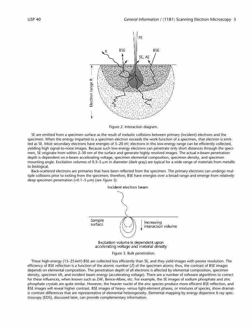
Figure 2. Interaction diagram.
SE are emitted from a specimen surface as the result of inelastic collisions between primary (incident) electrons and thespecimen. When the energy imparted to a specimen electron exceeds the work function of a specimen, that electron is emit-ted as SE. Most secondary electrons have energies of 5–20 eV; electrons in this low-energy range can be efficiently collected,yielding high signal-to-noise images. Because such low-energy electrons can penetrate only short distances through the speci-men, SE originate from within 2–30 nm of the surface and generate highly resolved images. The actual e-beam penetrationdepth is dependent on e-beam accelerating voltage, specimen elemental composition, specimen density, and specimenmounting angle. Excitation volumes of 0.5–5 mm in diameter (dark gray) are typical for a wide range of materials from metallicto biological.
Back-scattered electrons are primaries that have been reflected from the specimen. The primary electrons can undergo mul-tiple collisions prior to exiting from the specimen; therefore, BSE have energies over a broad range and emerge from relativelydeep specimen penetration (»0.1–5 mm) (see Figure 3).
Figure 3. Bulk penetration.
These high-energy (15–25 keV) BSE are collected less efficiently than SE, and they yield images with poorer resolution. Theefficiency of BSE reflection is a function of the atomic number (Z) of the specimen atoms; thus, the contrast of BSE imagesdepends on elemental composition. The penetration depth of all electrons is affected by elemental composition, specimendensity, specimen tilt, and incident beam energy (accelerating voltage). There are a number of software algorithms to correctfor these influences, when known such as ZAF, Bence-Albee, etc. For example, the SE images of sodium phosphate and zincphosphate crystals are quite similar. However, the heavier nuclei of the zinc species produce more efficient BSE reflection, andBSE images will reveal higher contrast. BSE images of heavy- versus light-element phases, or mixtures of species, show dramat-ic contrast differences that are representative of elemental heterogeneity. Elemental mapping by energy dispersive X-ray spec-troscopy (EDS), discussed later, can provide complementary information.
USP 40 General Information / á1181ñ Scanning Electron Microscopy 3

SAMPLE PREPARATION
As scanning electron microscopy has advanced as an analytical technique, different options have become available for sam-ple preparation. Ideally, the objective is to obtain the required image or chemical analysis of the material to be examined withas little intervention as possible. Additionally, one must consider the purpose of the analysis and the amount of material that isavailable. If the material to be examined is a foreign particulate in a parenteral product, sample preparation could be quitedifferent than if one is intending to image a bulk drug substance material or excipients. The decision tree (see Figure 4) belowrepresents a simplified version of the available sample preparation method and is one possible construct to determine the ap-propriate sample preparation method.
For example, in addition to metal (primarily aluminum) sample stubs there are also various metal meshes that can be usedto support samples. If the particle in question is isolated from liquid, the filter itself may serve as a suitable substrate for thepowder without having to transfer the sample to another sample holder. Additionally, adhesive carbon tabs are a commonmeans to secure the sample to the stub. There are a variety of other adhesive materials such as double-sided copper, silver andaluminum tape, or carbon and silver paint for this purpose.
Sample Coating
Historically, pharmaceutical materials, which are typically poor electrical conductors, had to be coated with a very thin layerof conductive material (carbon, gold, platinum, or other metals) to ensure that the electron beam used for imaging could bedissipated from the sample surface. Coating was also used to create a layer of “electron rich” material that would serve as asource for secondary electron emission.
With the advent of environmental scanning electron microscopy (ESEM) or variable pressure scanning electron microscopes,coating of non-conductive materials is no longer a prerequisite. The atmosphere in the sample chamber itself generates posi-tively charged ions that will dissipate any charge that accumulates on the sample surface.
4 á1181ñ Scanning Electron Microscopy / General Information USP 40
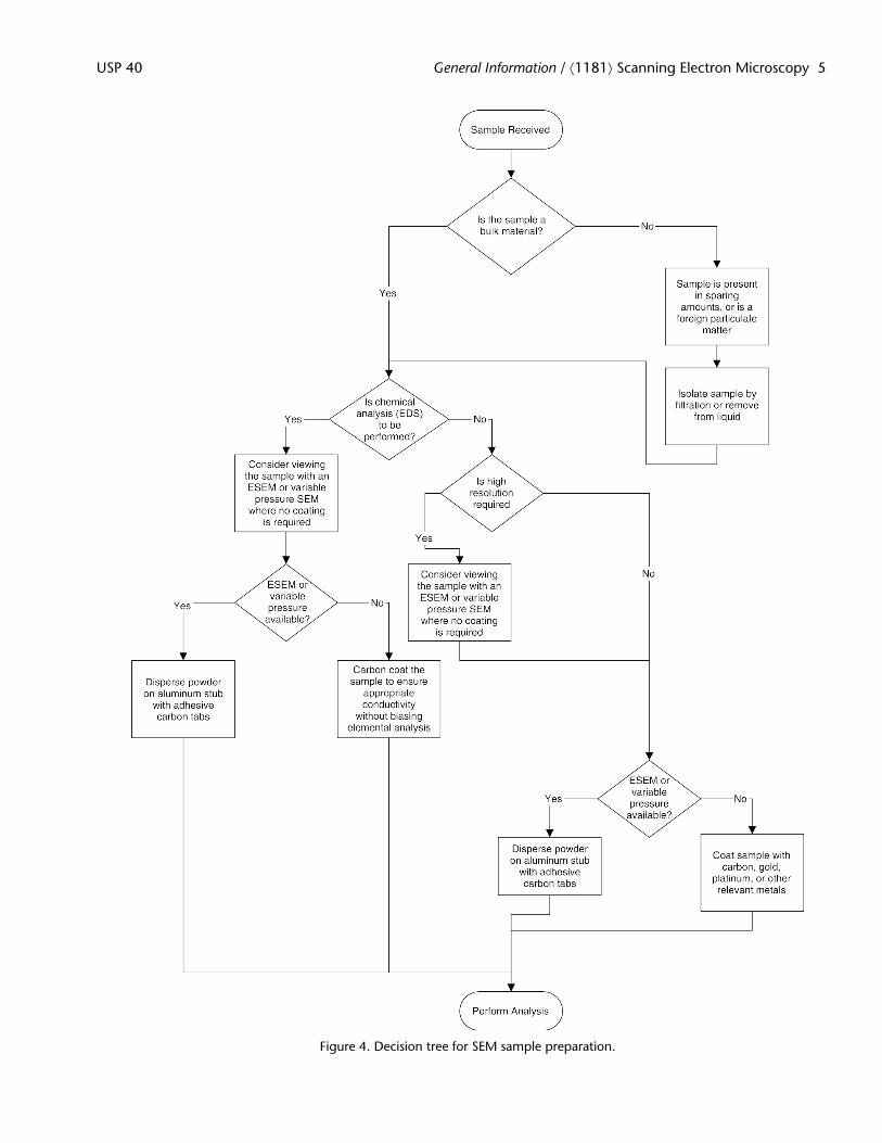
Figure 4. Decision tree for SEM sample preparation.
USP 40 General Information / á1181ñ Scanning Electron Microscopy 5
X-RAY GENERATION AND ELEMENTAL COMPOSITIONAL ANALYSIS
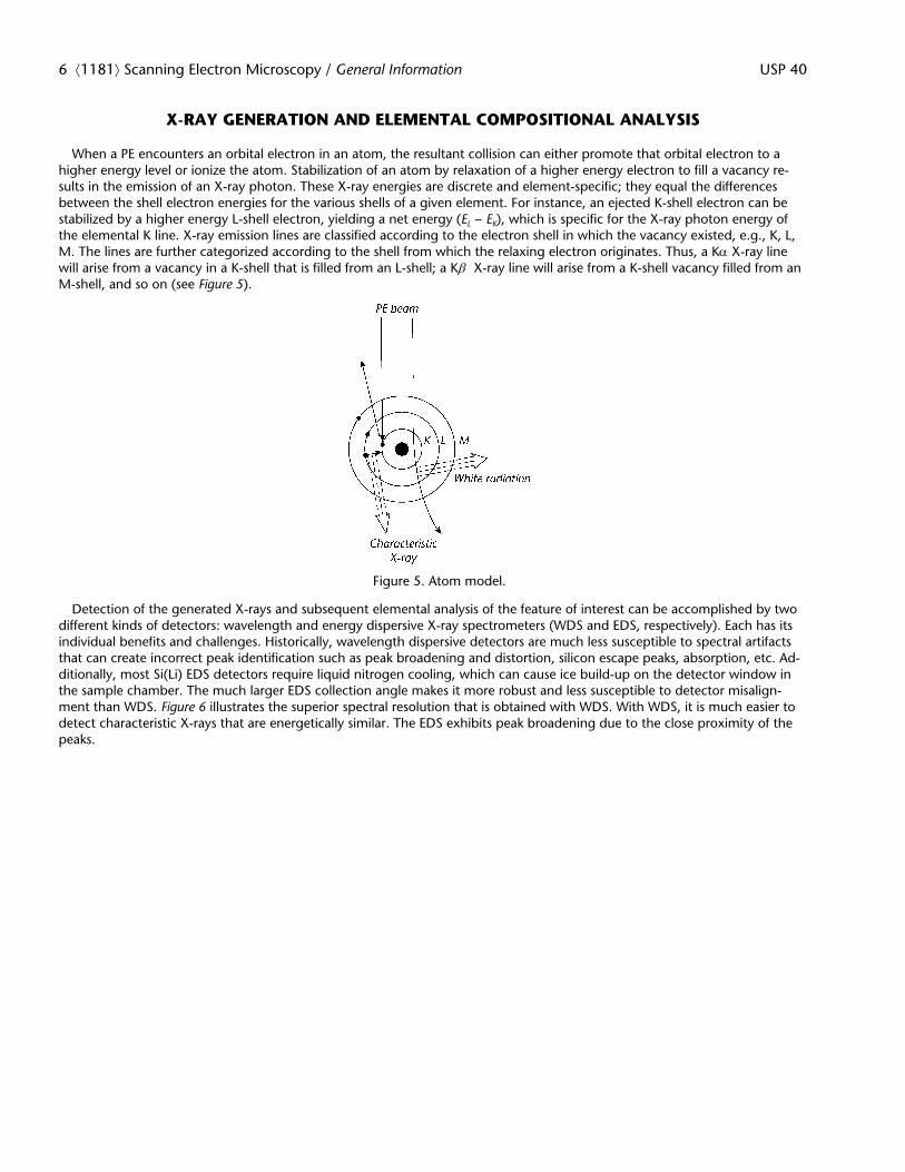
When a PE encounters an orbital electron in an atom, the resultant collision can either promote that orbital electron to ahigher energy level or ionize the atom. Stabilization of an atom by relaxation of a higher energy electron to fill a vacancy re-sults in the emission of an X-ray photon. These X-ray energies are discrete and element-specific; they equal the differencesbetween the shell electron energies for the various shells of a given element. For instance, an ejected K-shell electron can bestabilized by a higher energy L-shell electron, yielding a net energy (EL − EK), which is specific for the X-ray photon energy ofthe elemental K line. X-ray emission lines are classified according to the electron shell in which the vacancy existed, e.g., K, L,M. The lines are further categorized according to the shell from which the relaxing electron originates. Thus, a Ka X-ray linewill arise from a vacancy in a K-shell that is filled from an L-shell; a Kb X-ray line will arise from a K-shell vacancy filled from anM-shell, and so on (see Figure 5).
Figure 5. Atom model.
Detection of the generated X-rays and subsequent elemental analysis of the feature of interest can be accomplished by twodifferent kinds of detectors: wavelength and energy dispersive X-ray spectrometers (WDS and EDS, respectively). Each has itsindividual benefits and challenges. Historically, wavelength dispersive detectors are much less susceptible to spectral artifactsthat can create incorrect peak identification such as peak broadening and distortion, silicon escape peaks, absorption, etc. Ad-ditionally, most Si(Li) EDS detectors require liquid nitrogen cooling, which can cause ice build-up on the detector window inthe sample chamber. The much larger EDS collection angle makes it more robust and less susceptible to detector misalign-ment than WDS. Figure 6 illustrates the superior spectral resolution that is obtained with WDS. With WDS, it is much easier todetect characteristic X-rays that are energetically similar. The EDS exhibits peak broadening due to the close proximity of thepeaks.
6 á1181ñ Scanning Electron Microscopy / General Information USP 40

Figure 6. Example of spectral resolution obtained with wavelength-dispersive detectors where S Ka and Mo La can be clearlyresolved by WDS (gray peaks) but are not resolved by EDS (broad yellow peak). “Used by Permission. Courtesy of Oxford In-
struments.”
Advantages of EDS reside in the ease of use and speed to collect the entire X-ray spectrum making it ideal for the routineidentification of particles and features within a sample. The two types of detector technology most widely available for energydispersive X-ray spectroscopy (EDS) analysis are based on lithium-drifted silicon [Si(Li)] and silicon drift technology. While Si(Li)detectors have been around for the last 40 years, silicon drift detectors (SDD) have recently emerged as the preferred type dueto several key advantages including better detection of light elements (Z ³ 4), ability to handle high count rates, excellent ener-gy resolution even at high count rates, and even elimination of the need for liquid nitrogen to cool the detector prior to usedue to the use of Peltier cooling systems. While Si(Li) detectors were generally recommended to be run at 1,000–2,500 countsper second with an energy resolution of 129 eV at Mn-Ka, current SDD technology has superior energy resolution of 121 eVeven at the high count rate of 600,000 cps. For the average user, this means that the SDD detector may drastically shortenanalysis time provided that a high count rate may be obtained and with significantly better resolution for detection of lightelements. In practicality, the achievable count rate is determined by the accelerating voltage and probe current, solid angle ofthe detector and working distance to the sample, and ability of the sample to survive the electron beam without charging ormaterial change. Whether the user has an Si(Li) or SDD detector, it is a good rule of thumb to keep the dead time to 30% orbelow.
The elemental content of a specimen has a bearing on the selection of conditions for analysis. The most useful range of ac-celerating voltage is approximately 3–20 kV; most elements of interest can be ionized by electrons with energies in this range.The energy required in order to excite X-ray emission from a given line is termed its critical excitation potential. The criticalexcitation potential for a K line can be approximated by the sum of the primary line energies (Ka + La + Ma). Selection of anaccelerating voltage equal to 1.5 times this sum is usually sufficient for semi-quantitative analysis. For example, copper has Kaat 8.05 keV + La at 0.93 keV = 8.98 keV: and 1.5 × 8.98 keV = 13.47 keV. Selection of 15-kV accelerating voltage yields suffi-cient energy to ionize the K-shell of copper atoms and generate a useful analytical signal. It is generally suggested that EDSpractitioners should use the minimum accelerating voltage necessary to adequately excite the elements of interest (typically1.5–10 times the critical excitation energy). The interaction volume increases with increasing accelerating voltage, thus betterspatial resolution can be achieved by using lower accelerating voltage. Depending on the dimensions and density of the parti-cles, a signal from the substrate may be detected. Additionally, larger interaction volume causes increased absorbance and flu-orescence within the sample volume. Several accelerating voltages may be experimented with to determine the minimum ac-celerating voltage required. Routine use of a copper and a lighter metal standard such as aluminum allows quick verification ofelemental primary line energies bracketing the 0- to 10-keV range. An elemental collection for the metal standard prior to orwithin the experimental protocol is conducted to verify the primary line is ±0.04 keV of reference (but may depend upon thedetector manufacturer specification). This is a practical internal standard practice.
Inter-element interferences originate from many effects. High-energy X-rays emitted from heavy atoms can ionize lighter ele-ments to produce secondary X-ray emission from the lighter species. Lower high-Z element fluorescence and higher low-Z ele-ment fluorescence can be observed, in contrast to that expected from the PE-induced signal of a pure element. Conversely, X-
USP 40 General Information / á1181ñ Scanning Electron Microscopy 7
ray emission from a light element may be absorbed by a heavier matrix to yield a negative bias in the light-element signal.These effects always exist in heterogeneous specimens and must be corrected for during any quantitative analysis. A commonalgorithm, ZAF, may be used to correct for Z-dependent interferences due to absorption and secondary X-ray emission.
Point analysis and mapping are common analysis modes available for the identification of particles by EDS regardless of de-tector type. Most modern user interfaces allow the user to view a region of interest with secondary electron imaging and col-lect a spectrum for the entire region or a defined sub-region. Upon collecting an initial spectrum, it is important the user checkthat it appears satisfactory in terms of energy range for the elements present, optimum count rate, and is free from artifactssuch as charging. Once optimized for collection, the user can choose their preferred analysis mode to identify their sample.Point analysis is generally useful if different particle morphologies can be readily observed by SEM. The user can place a cross-hair at the center of each particle to collect a spectrum for later comparison. Care should be taken for the analysis of particlesless than 5 mm since the interaction volume may spread in the sample combined with the beam/sample interaction and canexcite electrons from the surrounding environment. This will produce spectral peaks that are not native to the feature of inter-est. For this reason, chemical analysis of small objects in an SEM is difficult. Other more surface-sensitive techniques such as X-ray photoelectron spectroscopy (XPS), scanning auger spectroscopy, and others provide more accurate spectral information.Orthogonal analysis, both within and outside any given technique, is of great value.
When there is no obvious morphological difference for a collection of particles, EDS mapping may be the best mode of anal-ysis. In this mode, the EDS detector collects information as the electron beam rasters across the sample, thus the elementalinformation is in registry with the SE/BSE image. The user can define the region of interest from the entire region observable inthe SE/BSE image to a sub-region. Additionally, the user can define the scan speed, dwell time/pixel, and resolution of the mapto suit their needs in terms of speed or resolution. A significant factor to consider for EDS mapping is that the X-ray signal willvary based on the surface texture and slope of the particle's surface. In the most severe case, a shadow may be observed if thatsurface is no longer within the line of sight of the detector. It may be possible to minimize these artifacts due to tilting thesample further towards the detector. It is often useful to map the elements of interest versus an element that does not exist inthe sample. The X-ray counts for the non-existent element should provide a uniform background across the entire region if thesurface is level.
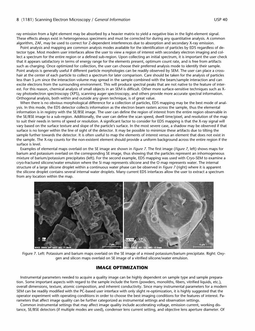
Examples of elemental maps overlaid on the SE image are shown in Figure 7. The first image (Figure 7, left) shows maps forbarium and potassium overlaid on the corresponding SE image, thus showing that the particles represent an inhomogeneousmixture of barium/potassium precipitates (left). For the second example, EDS mapping was used with Cryo-SEM to examine acryo-fractured silicone/water emulsion where the Si map represents silicone and the O map represents water. The internalstructure of a large silicone droplet within a continuous water phase can be observed in Figure 7 (right) where it is apparentthe silicone droplet contains several internal water droplets. Many current EDS interfaces allow the user to extract a spectrumfrom any location within the map.
Figure 7. Left: Potassium and barium maps overlaid on the SE image of a mixed potassium/barium precipitate. Right: Oxy-gen and silicon maps overlaid on SE image of a vitrified silicone/water emulsion.
IMAGE OPTIMIZATION
Instrumental parameters needed to acquire a quality image can be highly dependent on sample type and sample prepara-tion. Some important aspects with regard to the sample include the form (powders, monoliths, fibers, vitrified liquids, etc.),overall dimensions, texture, atomic composition, and inherent conductivity. Since many instrumental parameters for a modernSEM can be readily modified with the PC-based user interface with only slight re-optimization, it is highly suggested that theoperator experiment with operating conditions in order to choose the best imaging conditions for the features of interest. Pa-rameters that affect image quality can be further categorized as instrumental settings and observation settings.
Common instrumental settings that may affect image quality include accelerating voltage, emission current, working dis-tance, SE/BSE detectors (if multiple modes are used), condenser lens current setting, and objective lens aperture diameter. Of
8 á1181ñ Scanning Electron Microscopy / General Information USP 40
these, the accelerating voltage may be the most important instrumental parameter since it directly affects the penetrationdepth of incident electrons thereby determining the features that can be observed. In general, choosing the optimal accelerat-ing voltage is a balance of achieving the best contrast for the features that the user is most interested in, while minimizingunwanted effects such as loss of topographic information or charging. The best approach to choosing an ideal acceleratingvoltage for an unknown sample is to experiment with up to 3 accelerating voltages (e.g., 1, 3, and 10 kV), then choose thebest one to continue to further optimize the image. The working distance and choice of SE/BSE detector are normally chosenin combination depending on the desired resolution, depth of focus, and sample tilt. Generally, shorter working distances re-sult in higher resolution but less depth of focus. Likewise, based on the position the SE detectors are placed in the column, atradeoff exists for spatial resolution versus surface topography, where upper detectors generally detect a high resolution SEsignal and lower detectors show more surface topography. Lastly, the condenser lens setting and objective lens aperture diam-eter can be optimized to provide the ideal specimen current, resolution, and depth of focus required for a specific sample type.
Upon choosing an initial set of instrumental conditions as mentioned above, basic image observation can be optimized inthe following manner:
(1) Select a low magnification (1000–3000×) initially(2) Course adjust image brightness(3) Course adjust focus(4) Select an easy-to-visualize area of the specimen(5) Check/adjust to optimize the electromagnetic alignment of the electron optics (beam, aperture, stigmation)(6) Select a feature of interest at higher magnification(7) Adjust focus and astigmatism(8) Adjust image brightness and contrast(9) Collect image.Image collection can be accomplished using different resolutions (1280 × 960 is most common) and capture speeds using
either slow scan collection or frame integration. In general, slow scan collection is used to collect high-resolution imageswhereas frame integration is used for specimen types that have charging or stability issues. A collection using a higher captureresolution, slower scan speed, or additional frames may improve the image resolution, however the user must take caution ofthe increased likelihood of specimen drift over this period which would negate any benefit.
FORENSIC ANALYSIS OF PARTICLES
Shape Analysis
Because of the three-dimensional nature of images obtained via scanning electron microscopy, particle shape provides agreat deal of information about the composition and source of the particle without obtaining a chemical analysis via EDS.
The most commonly identified particles found in pharmaceutical compounds generally fall into several distinct categories.Note that particles in parenteral products arise from three general sources: (a) extrinsic or outside of the product, as truly for-eign solids; (b) intrinsic or associated with the product, its package or manufacture; (c) inherent particles expected to composethe formulation, such as proteins in biotherapeutic products (see Subvisible Particulate Matter in Therapeutic Protein Injectionsá787ñ), and may be encountered when probing those formulae. Some examples of extrinsic particles are the following:
• Corrosion products from one or more equipment sources, and may occur from formulation interaction• Materials from the manufacturing environment such as cellulose (from paper bags), extraneous fibers (clothing, filters,
etc.)• Inhomogeneities in the product, specifically incomplete mixing (for solid oral dosage products) that can create cosmetic
or elegance issues with tablets• Environmentally-sourced biological materials• Material that has been exposed to extreme heat that might char. The causes for this can vary from paper pyrolized during
depyrogenation to material sticking to components that are exposed to friction (powder milling, compaction, etc.). If resi-due unintentionally builds up in these areas, the exposure to friction can decompose the material, making it appearburnt.
Figure 8 shows representative images of some of the particulate matter mentioned above that the user might encounter in aforensic investigation.
USP 40 General Information / á1181ñ Scanning Electron Microscopy 9

Figure 8. Scanning electron micrographs of commonly found particles in pharmaceutical manufacturing areas: A. cotton fi-bers, B. glass particles, C. Teflon shavings, D. aluminum shavings. (All of the images provided courtesy of McCrone Atlas
(www.mccroneatlas.com.)
Interpretation of a particle’s origin from characteristics observed by SEM analysis depends on the particle features; for in-stance, any particle with sharp corners and well-defined edges is made from a material that is not soluble in the product liquid.If it is transparent to the beam, then the user could conclude it consists of very low Z elements. Crystalline particles exhibitobvious symmetry and growth patterns. Slow growth is characterized by large crystals and fast growth by small, often aggre-gated crystal masses.
Particle morphology and surface characteristics may be helpful in sourcing unknowns. Aspect ratio, or the ratio of the lengthof a particle divided by its width, indicates fibrous materials. Analysis by optical microscopy often serves as a more effectivetool to analyze fibers by determining diagnostic optical properties (refractive indices, birefringence, elongation, etc.) usingplane and crossed polarized light that can distinguish among various possible sources. With a scanning electron microscope,however, elemental analysis can determine (a) if the fiber is inorganic or organic and (b) the presence of surface additives.Scanning electron microscopy also offers the added benefit of being able to image at much higher magnification to revealmorphological structures of biological origin or features indicative of commercial manufacture.
As mentioned previously, different kinds of electrons are emitted when an electron beam interacts with a solid surface. Thetwo most useful types of electrons are secondary and back-scattered. By choosing the appropriate detector or instrument setup, the image can be biased towards one or the other. Back-scattered electrons can provide useful information regarding thechemical composition of the feature in question. If the instrument is set up to use BSE to form the image, elements possessinghigher atomic mass will appear brighter than those having a lower atomic mass. By selecting this imaging mode, organic parti-cles are easily distinguished from metallic debris, for example. For instance, at low kV, glass or plastic may appear as solid ob-jects, whereas at higher kV they may appear somewhat transparent. Further, appearance at low kV on a tungsten filament SEMmay mean something completely different than that at low kV on an FE SEM or environmental SEM. Different materials requiredifferent operating conditions to suitably image using SE, to prevent charging and to improve contrast. Typically, use low kV(3 kV or less using a semi-in-lens or in-lens FE SEM) for non-conductive materials such as glass and plastic. If the material isextremely thin (<100 nm), the material can be visualized in transmission mode (STEM) as well as SE mode.
GENERAL REFERENCES
1. Goldstein, J., et al., Scanning Electron Microscopy and X-ray Microanalysis. Third ed. 2003, New York: Springer.
10 á1181ñ Scanning Electron Microscopy / General Information USP 40

2. Echlin, P., Handbook of Sample Preparation for Scanning Electron Microscopy and X-ray Microanalysis. 2010, New York:Springer. 330.
3. Reimer, L., Scanning Electron Microscopy: Physics of Image Formation and Microanalysis. Springer Series in Optical Sciences,ed. H.K.V. Lotsch. Vol. 45. 1998, New York: Springer.
USP 40 General Information / á1181ñ Scanning Electron Microscopy 11