Embed Size (px)
Citation preview

Sam Palermo Analog & Mixed-Signal Center
Texas A&M University
ECEN474: (Analog) VLSI Circuit Design Fall 2012
Lecture 5: Layout Techniques

Announcements
• HW1 due today at 5PM • For grad students, confirm that you
participated in the Analog IC Design Olympics on the first page of your homework 1 solution
• Turn into my mailbox in WERC 315
• Exam 1 on Wednesday Sep. 26
• Previous semester exams posted on website • One double-sided 8.5x11 notes page allowed • Bring your calculator
2

Agenda
• MOS Fabrication Sequence • CMOS Design Rules • Layout Techniques • Layout Examples
• Reference Material
• Razavi Chapter 17 & 18
3

ECEN-474-2009 Jose Silva-Martinez
4
Fundamentals on Layout Techniques: N-Well CMOS Technologies
Substrate is always connected to the most negative voltage, and is shared by all N-type transistors
N
P+ N+ P+
N-Well
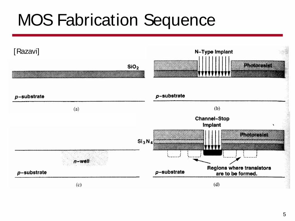
MOS Fabrication Sequence
5
[Razavi]
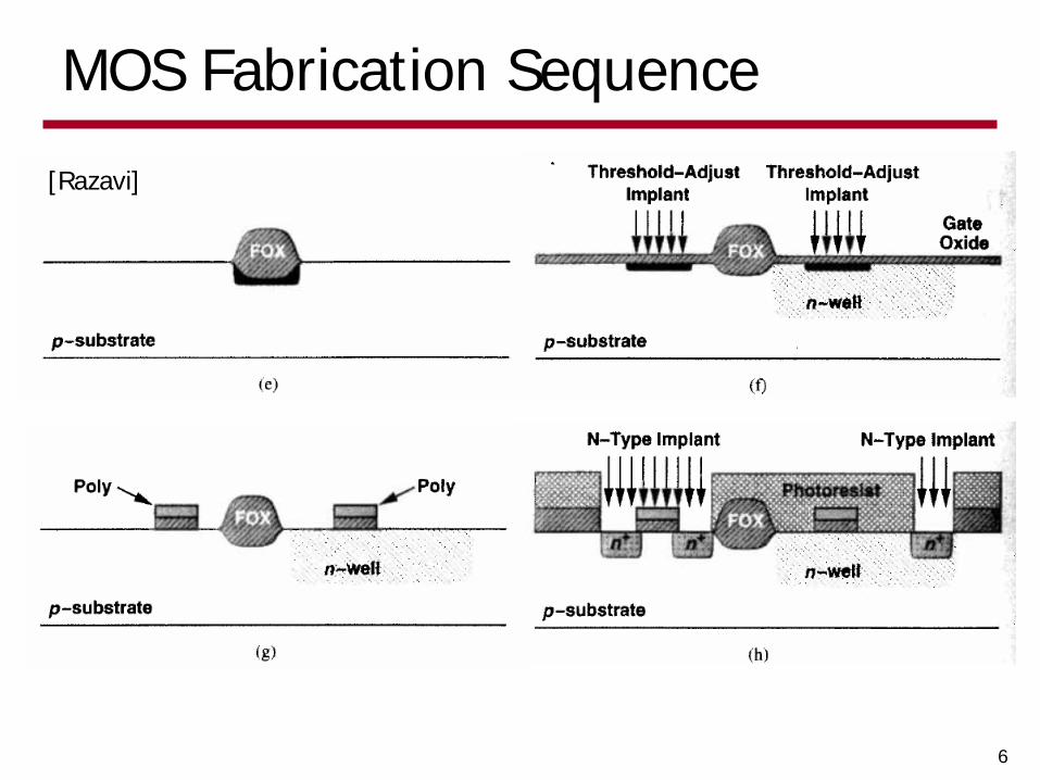
MOS Fabrication Sequence
6
[Razavi]

MOS Fabrication Sequence
7
“Front-End”
“Back-End”
[Razavi]
• A “silicide” step, where highly conductive metal is deposited on the gate and diffusion regions, reduces transistor terminal resistance
• To prevent potential gate-source/drain shorting an “oxide spacer” is first formed before silicide deposition

Contact and Metal Fabrication
8
[Razavi]

Transistor Geometries
9
• Minimum drawing feature = λ • Assume w.c. mask alignment <0.75λ • Relative misalignment between 2
masks is <1.5λ
sides) (3
XWPSPSXWASAD
LWAGate
2,*,
*
+==
=λ
2λ
5λ
2λ
W 2λ λ4λ
L
X
• X depends on contact size • 5λ in this example
• λ-based design rules allow a process and feature size-independent way of setting mask dimensions to scale • Due to complexity of modern processing, not used often today

ECEN-474-2009 Jose Silva-Martinez
10
Physical Layer N-well Silicon Nitride Polysilicon Layer 1 Polysilicon Layer 2 P+ Ion Implant N+ Ion Implant Contact cut to n+/p_
Metal 1 Via Oxide Cuts Metal 2 Pad Contact (Overglass)
BASIC SCNA CMOS LAYERS
N-channel MOSFET
P-channel MOSFET
Source Drain
Poly Gate
Gate Oxide
p substrate
Bulk
n+ n+
Metal 1CVD Oxide
SourceDrain
Poly Gate
Gate Oxide
p substrate
Bulk
p+ p+
Metal 1CVD Oxide
n-well Bulk

ECEN-474-2009 Jose Silva-Martinez
11
S
X
d
d
n+Metal
x
Minimum width and spacing
(a) Mask definition (b) After annealing
Patterning sequence for a doped n+ line.
(a) Contact size
(b) Side view Geometry of a contact
cut
Depletion regions due to parallel n+ lines Contact spacing rule
(a) Masking Design
(b) Registration tolerance
Design Rule Basics X
Implanted dopantsp, Na
X
p, Na
n+
p, Na
n+Nd
n+Nd
Depletionregions
xpS
n+ n+
p, Na
n+
Metal
ECEN-474-2009 Jose Silva-Martinez
12
Nselect
Active
p-Substrate
n+
Nselect
Active
p-Substrate
n+
Active area border
s
W
Poly gate
Active area border
W
Poly gate
s
Poly gate Poly gate
substrate
Metalpoly
Resist
substrate
Metal
substrate
Metal
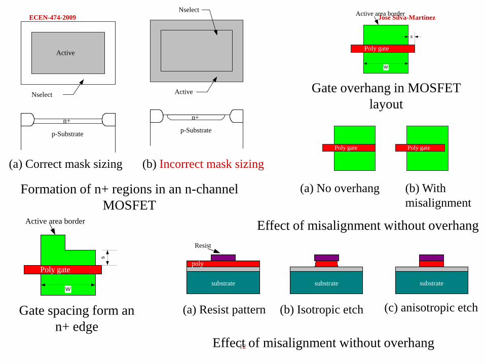
(a) Correct mask sizing
Formation of n+ regions in an n-channel MOSFET
(b) Incorrect mask sizing
Gate spacing form an n+ edge
Gate overhang in MOSFET layout
Effect of misalignment without overhang
(a) No overhang (b) With misalignment
Effect of misalignment without overhang
(a) Resist pattern (b) Isotropic etch (c) anisotropic etch

ECEN-474-2009 Jose Silva-Martinez
13
Mask Number Mask Layer
1 NWELL
2 ACTIVE
3 POLY
4 SELECT
5 POLY CONTACT
6 ACTIVE CONTACT
7 METAL1
8 VIA
9 METAL2
10 PAD
11 POLY2
Nselect
Active
W'
L'
n+ n+L
Poly
W
Side View
FrontView
Difference between the drawn and physical values for channel length and the channel width
Design Rule Layers

ECEN-474-2009 Jose Silva-Martinez
14
Metal DrainPolysilicon Gate
Gate Oxide
p substrate (Bulk)
Bulk
n+n+Fieldoxide L n+n+
L'
xoxPolysilicon
Gate
p
W
Structure of a n-channel MOSFET Perspective view of an n-channel MOSFET
n+/p+n+/p+
PolyActivecontact Poly
contact
Example of Layout Rules
• Minimum transistor width is set by minimum diffusion width • 2 or 3λ (check with TA)
• Often, we use a use a slightly larger “minimum” that is equal to the contact height (4λ in this example)
λ
λ 2λ
2λ
2λ
2λ
2 or 3λ
λ 2λ λ

ECEN-474-2009 Jose Silva-Martinez
15
Drain Source
Gate
Bulk
DrainSource
Gate
Bulk
L
Poly n+n+ W
L
Poly n+n+ W
n-well
N-channel MOSFET P-channel MOSFET
(a) Cross section
(b) Circuit symbol
(c) Top view
Source Drain
Poly Gate
Gate Oxide
p substrate
Bulk
n+ n+
Metal 1CVD Oxide
SourceDrain
Poly Gate
Gate Oxide
p substrate
Bulk
p+ p+
Metal 1CVD Oxide
n-well Bulk

ECEN-474-2009 Jose Silva-Martinez
16
PolyMetal 1
N+/P+Contact
D
S
G
VDD
Gnd
Mp
Mn
OutIn
VDD
Gnd
Mp
Mn
Out
In
Stick Diagrams
(a) Definitions (b) MOSFET
Stick diagrams for the CMOS Inverter
ECEN-474-2009 Jose Silva-Martinez
17
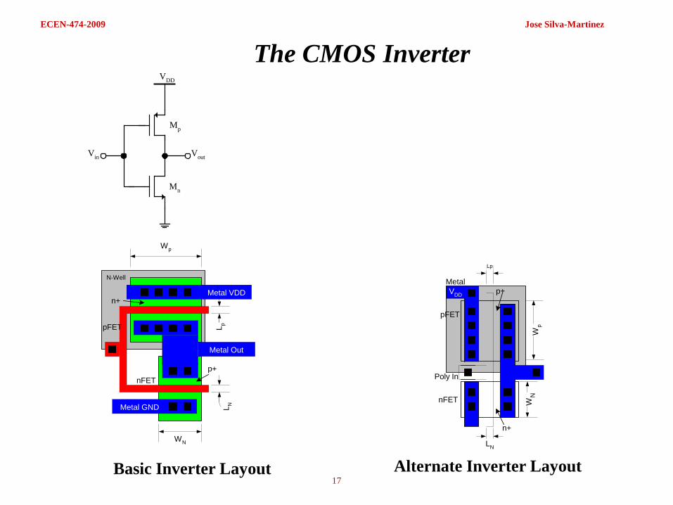
Mp
Mn
Vin Vout
VDD
WN
L N
L p
Wp
Metal GND
N-Well
n+
pFET
nFETp+
Metal Out
Metal VDD
Poly In
pFET
nFET
MetalVDD p+
n+
Lp
LN
WN
Wp
The CMOS Inverter
Basic Inverter Layout Alternate Inverter Layout

ECEN-474-2009 Jose Silva-Martinez
18
MnB
MpB MpA
MnAA
B
Vo
MnB
MpB
MpA
MnA
A BVo
pFET
nFET
Metal VDD
n+
Metal GND
Out
A B
pFET
nFET
p+
Metal GND
Out
A B
Metal VDD
CMOS NAND2 logic gate
CMOS NOR2 logic gate
Standard Cells: VDD, VSS and output run in Parallel

ECEN-474-2009 Jose Silva-Martinez
19
Wide Analog Transistor: Analog techniques
• Unacceptable drain and source resistance
• Stray resistances in transistor structure
• Contacts short the distributed resistance of diffused areas
Most of the current will be shrunk to this side Current is spread

ECEN-474-2009 Jose Silva-Martinez
20
• Orientation is important in analog circuits for matching purposes
Transistor orientation
ECEN-474-2009 Jose Silva-Martinez
21
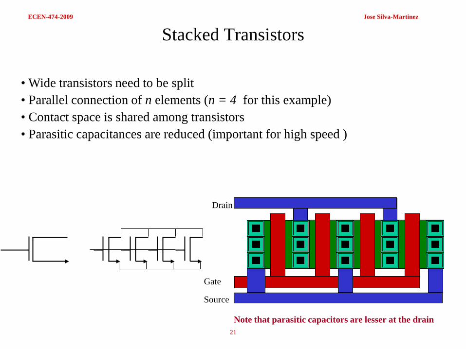
Stacked Transistors
• Wide transistors need to be split • Parallel connection of n elements (n = 4 for this example) • Contact space is shared among transistors • Parasitic capacitances are reduced (important for high speed )
Source
Gate
Drain
Note that parasitic capacitors are lesser at the drain

ECEN-474-2009 Jose Silva-Martinez
22
Matched Transistors
Drain M1 Drain M2
Source
• Simple layouts are prone to process variations, e.g. VT, KP, Cox • Matched transistors require elaborated layout techniques
M1 M2
Process Variations Differential pair requiring “matched transistors”
ECEN-474-2009 Jose Silva-Martinez
23
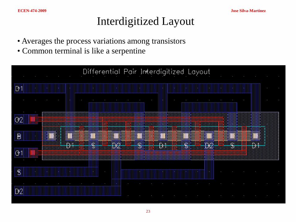
Interdigitized Layout • Averages the process variations among transistors • Common terminal is like a serpentine

ECEN-474-2009 Jose Silva-Martinez
24
M1 M2 M2 M1 M1 M2 M2 M1
KP=1 KP2 KP3 KP4 KP5 KP6 KP7 KP8
• Process variations are averaged among transistors KPs for M1: KP1+KP4+KP5+KP8 M2: KP2+KP3+KP6+KP7
• Technique maybe good for matching dc conditions • Uneven total drain area between M1 and M2. This is undesirable for ac
conditions: capacitors and other parameters may not be equal • A more robust approach is needed (Use dummies if needed !!)
Why Interdigitized?
ECEN-474-2009 Jose Silva-Martinez
25
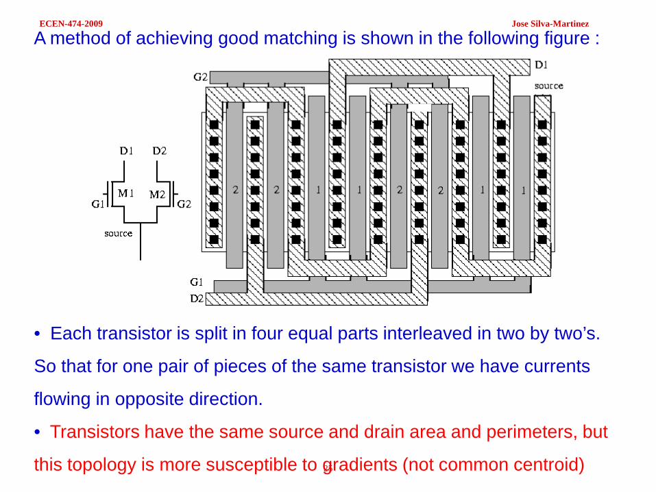
A method of achieving good matching is shown in the following figure :
• Each transistor is split in four equal parts interleaved in two by two’s.
So that for one pair of pieces of the same transistor we have currents
flowing in opposite direction.
• Transistors have the same source and drain area and perimeters, but
this topology is more susceptible to gradients (not common centroid)

ECEN-474-2009 Jose Silva-Martinez
26
Common Centroid Layouts Usually routing is more complex
M1 M2 M1 M2
M2 M1 M2 M1
M1 M2 M1 M2
M2 M1 M2 M1
0 1 2 3
0
1
2
3 CENTROID (complex layout) M1: 8 transistors (0,3) (0,1) (1,2) (1,0) (2,3) (2,1) (3,2) (3,0) M2: 8 transistors (0,2) (0,0) (1,3) (1,1 (2,2) (2,0) (3,3) (3,1)
ECEN-474-2009 Jose Silva-Martinez
27
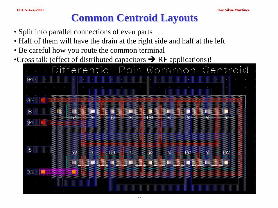
Common Centroid Layouts • Split into parallel connections of even parts • Half of them will have the drain at the right side and half at the left • Be careful how you route the common terminal •Cross talk (effect of distributed capacitors RF applications)!

ECEN-474-2009 Jose Silva-Martinez
28
•Many contacts placed close to one another reduces series resistance and make the surface of metal connection smoother than when we use only one contact; this prevents microcraks in metal;
• Splitting the transistor in a number of equal part connected in parallel reduces the area of each transistor and so reduces further the parasitic capacitances, but accuracy might be degraded!

ECEN-474-2009 Jose Silva-Martinez
29
Diffusion resistors
Diffused resistance
Diffused resistance
well resistance
Pinched n-well resistance
ECEN-474-2009 Jose Silva-Martinez
30
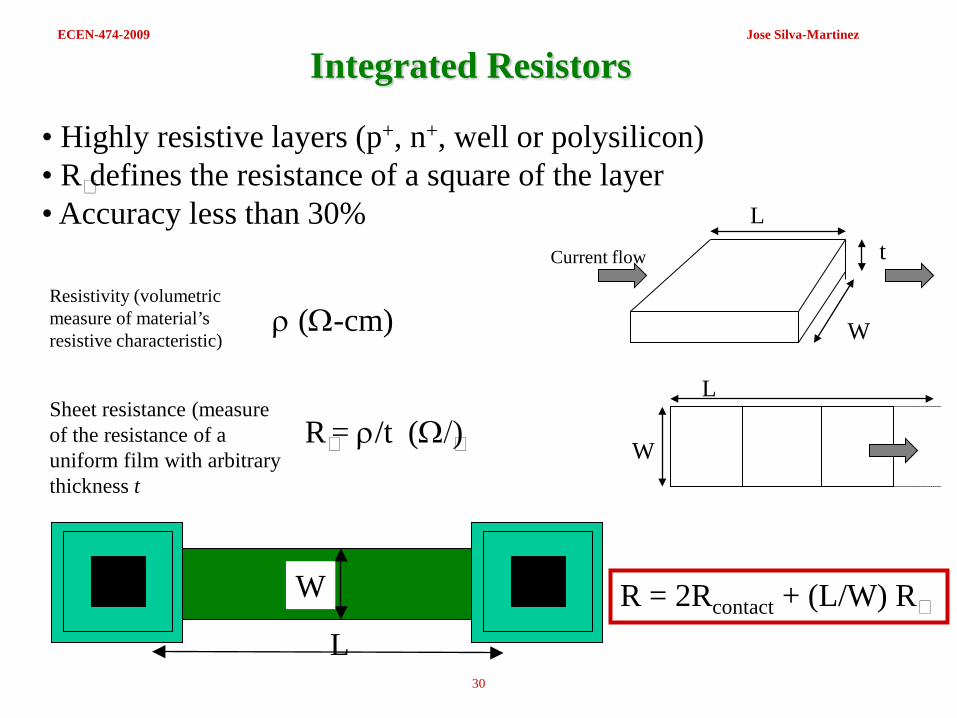
Integrated Resistors
L
W R = 2Rcontact + (L/W) R
• Highly resistive layers (p+, n+, well or polysilicon) • R defines the resistance of a square of the layer • Accuracy less than 30%
R = ρ/t (Ω/)
ρ (Ω-cm)
L t
W
L
W
Resistivity (volumetric measure of material’s resistive characteristic)
Sheet resistance (measure of the resistance of a uniform film with arbitrary thickness t
Current flow

ECEN-474-2009 Jose Silva-Martinez
31
TYPICAL INTEGRATED RESISTORS
RWLR2R cont +=
Sheet Resistance
W/0 30 - 50
50 -150
2K - 4K
3K - 6K
6K - 10K
9K - 13K
20 - 40
15 - 40
Accuracy
% 20 - 40
20 - 40
15 - 30
15 - 30
25 - 40
25 - 40
25 - 40
25 - 40
Temperature Coefficient
ppm/oC 200 - 1K
200 - 1K
5K
5K
10K
10K
500 - 1500
500 - 1500
Voltage Coefficient
ppm/V 50 - 300
50 - 300
10K
10K
20Κ
20Κ
20 - 200
20 - 200
Type of layer
n + diff
p + diff
n - well
p - well
pinched n - well
pinched p - well
first poly
second poly
L
W
Special poly sheet resistance for some analog processes might be as high as 1.2 KΩ/

ECEN-474-2009 Jose Silva-Martinez
32
In order to implement large resistors : • Use of long strips (large L/W)
• Use of layers with high sheet resistance (bad performances) Layout : rectangular “serpentine”
jxWLR
WLR ρ
⋅==
Large Resistors
ECEN-474-2009 Jose Silva-Martinez
33
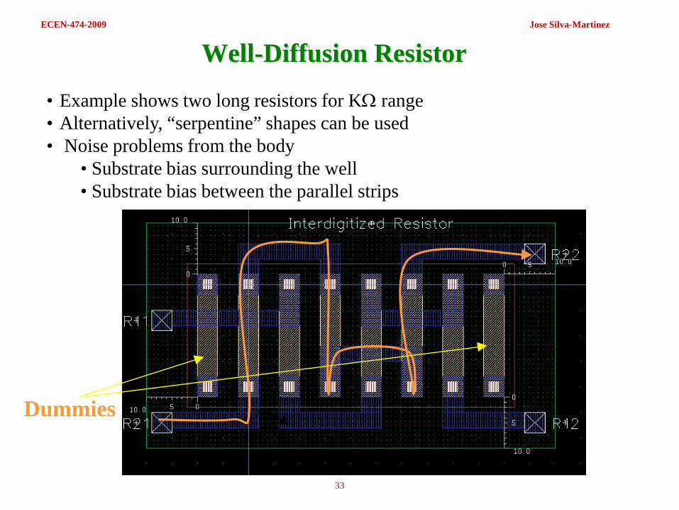
Well-Diffusion Resistor
• Example shows two long resistors for KΩ range • Alternatively, “serpentine” shapes can be used • Noise problems from the body
• Substrate bias surrounding the well • Substrate bias between the parallel strips
Dummies

ECEN-474-2009 Jose Silva-Martinez
34
Factors affecting accuracy : Plastic packages cause a large pressure on the die (= 800 Atm.). It determines a variation of the resistivity. For <100> material the variation is unisotropic, so the minimum is obtained if the resistance have a 45o orientation. Temperature : Temperature gradient on the chip may produce thermal induced mismatch.
uncompensated
compensated

ECEN-474-2009 Jose Silva-Martinez
35
Etching
Wet etching : isotropic (undercut effect) HF for SiO2 ; H3PO4 for Al ∆x for polysilicon may be 0.2 – 0.4 µm with standard deviation 0.04 – 0.08 µm. Reactive ion etching (R.I.E.)(plasma etching associated to “bombardment”) : unisotropic. ∆x for polysilicon is 0.05 µm with standard deviation 0.01 µm Boundary : The etching depends on the boundary conditions • Use dummy strips
ECEN-474-2009 Jose Silva-Martinez
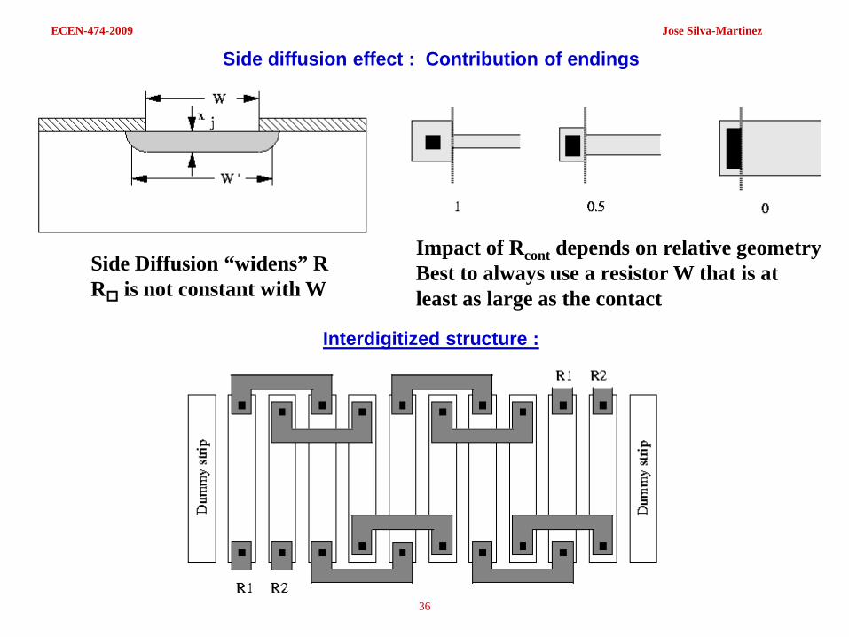
Side diffusion effect : Contribution of endings
Interdigitized structure :
36
Side Diffusion “widens” R R is not constant with W
Impact of Rcont depends on relative geometry Best to always use a resistor W that is at least as large as the contact

ECEN-474-2009 Jose Silva-Martinez
37
First polysilicon resistance
First polysilicon resistance with a well shielding
Second polysilicon resistance
Second polysilicon resistance with a well shielding
Poly Resistors
2

ECEN-474-2009 Jose Silva-Martinez
38
Typical Resistance Process Data 0.8 µm process
Sheet Resistance (Ω/)
Contact Resistance
(Ω) N+Actv 52.2 66.8 P+Actv 75.6 37.5 Poly 36.3 30.6 Poly 2 25.5 20.7 Mtl 1 0.05 0.05 Mtl 2 0.03 N-Well 1513
Gate oxide thickness 316 angstroms

ECEN-474-2009 Jose Silva-Martinez
39
TYPES OF INTEGRATED CAPACITORS
Electrodes : metal; polysilicon; diffusion
Insulator : silicon oxide; polysilicon oxide; CVD oxide
222
ox
ox2
r
r2
WW
LL
tt
CC
∆
+
∆
+
∆+
εε∆
=
∆
WLt
Cox
oxε=
TOP VIEW

ECEN-474-2009 Jose Silva-Martinez
40
Factor affecting relative accuracy/matching
εε∆
ox
ox
∆
ox
oxtt
∆
∆
WW;
LL
• Oxide damage
• Impurities
• Bias condition
• Bias history (for CVD)
• Stress
• Temperature
• Etching
• Alignment
• Grow rate
• Poly grain size
222
ox
ox2
r
r2
WW
LL
tt
CC
∆
+
∆
+
∆+
∆=
∆
εε
%1.01CC
−≈∆
Note, the absolute C may vary as high as 20% due to process variations

ECEN-474-2009 Jose Silva-Martinez
41
Poly1 - Poly2 Capacitor
• Area is determined by poly2 • Problems
• undercut effects • nonuniform dielectric thickness • matching among capacitors •Minimize the rings (inductors)
Poly 2
Poly 1
ECEN-474-2009 Jose Silva-Martinez
42
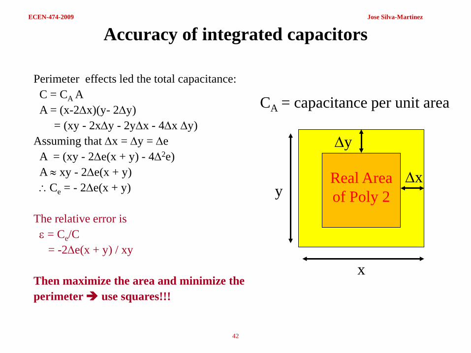
Accuracy of integrated capacitors
Perimeter effects led the total capacitance: C = CA A A = (x-2∆x)(y- 2∆y) = (xy - 2x∆y - 2y∆x - 4∆x ∆y)
Assuming that ∆x = ∆y = ∆e A = (xy - 2∆e(x + y) - 4∆2e) A ≈ xy - 2∆e(x + y) ∴Ce = - 2∆e(x + y)
The relative error is ε = Ce/C = -2∆e(x + y) / xy
Then maximize the area and minimize the perimeter use squares!!!
x
y ∆x
∆y
CA = capacitance per unit area
Real Area of Poly 2
ECEN-474-2009 Jose Silva-Martinez
43
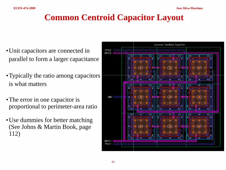
•Unit capacitors are connected in parallel to form a larger capacitance
•Typically the ratio among capacitors is what matters
•The error in one capacitor is proportional to perimeter-area ratio
•Use dummies for better matching (See Johns & Martin Book, page 112)
Common Centroid Capacitor Layout

ECEN-474-2009 Jose Silva-Martinez
44
Common centroid structures
C1
TC1
C5
TC5
C2
TC2
C3
TC3
C4
TC4
C2 = C1 C3 = 2C1 C4 = 4C1 C5 = 8C1

ECEN-474-2009 Jose Silva-Martinez
45
Be aware of parasitic capacitors
Polysilicon-Polysilicon: Bottom plate capacitance is comparable (10-30 %) with the poly-poly capacitance
Metal1-Metal2: More clean, but the capacitance per micrometer square is smaller. Good option for very high frequency applications ( C~ 0.1-0.3 pF).
C1 CP1 CP2’’
CP2’
poly2
poly1
substrate
CP1, CP2’’ are very small (1-5 % of C1) CP2’ is around 10-50 % of C1
C1
CP1 CP2
metal2
metal1
substrate
Thick oxide
C1
CP1 CP2
“Floating” Capacitors
CP2 is very small (1-5 % of C1)

ECEN-474-2009 Jose Silva-Martinez
46
Typical Capacitance Process Data (See MOSIS webside for the AMI 0.6 CMOS process)
Capacitance N+Actv P+Actv Poly Poly 2 Mtl 1 Mtl 2 UNITS
Area (substrate)
292 290 35 20 13 aF/ µ m 2
Area ( N+active)
1091 684 49 26 aF/ µ m 2
Area ( P+active)
1072 677 aF/ µ m 2
Area ( poly) 599 45 23 aF/ µ m 2
Area (poly2) 45 aF/ µ m 2
Area (metal1) 42 aF/ µ m 2
Fringe (substrate)
80 170 36 25 aF/ µ m
Fringe ( poly) 59 39 aF/ µ m
900
a=10-18, f=10-15, p=10-12, n=10-9 µ=10-6, m=10-3
ECEN-474-2009 Jose Silva-Martinez
47
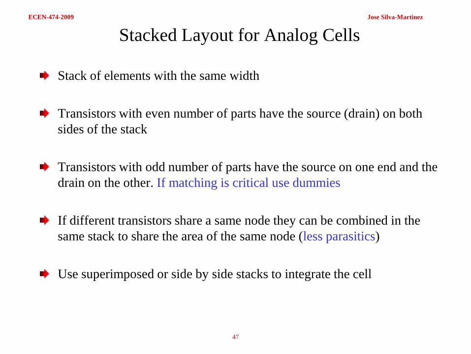
Stacked Layout for Analog Cells
Stack of elements with the same width Transistors with even number of parts have the source (drain) on both sides of the stack Transistors with odd number of parts have the source on one end and the drain on the other. If matching is critical use dummies If different transistors share a same node they can be combined in the same stack to share the area of the same node (less parasitics) Use superimposed or side by side stacks to integrate the cell
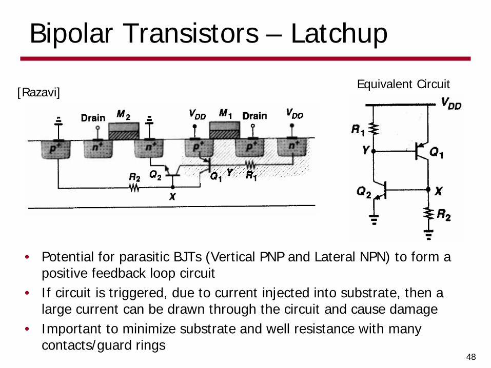
Bipolar Transistors – Latchup
• Potential for parasitic BJTs (Vertical PNP and Lateral NPN) to form a positive feedback loop circuit
• If circuit is triggered, due to current injected into substrate, then a large current can be drawn through the circuit and cause damage
• Important to minimize substrate and well resistance with many contacts/guard rings
48
Equivalent Circuit [Razavi]

ECEN-474-2009 Jose Silva-Martinez
49
Analog Cell Layout • Use transistors with the same orientation
• Minimize S/D contact area by stacking transistors (to
reduce parasitic capacitance to substrate)
• Respect symmetries
• Use low resistive paths when current needs to be carried (to avoid parasitic voltage drops)
• Shield critical nodes (to avoid undesired noise injection)
• Include guard rings everywhere; e.g. Substrate/well should not have regions larger than 50 um without guard protections (latchup issues)
ECEN-474-2009 Jose Silva-Martinez
50
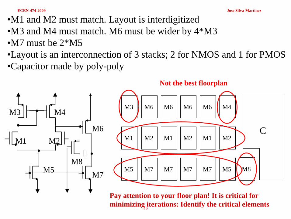
•M1 and M2 must match. Layout is interdigitized •M3 and M4 must match. M6 must be wider by 4*M3 •M7 must be 2*M5 •Layout is an interconnection of 3 stacks; 2 for NMOS and 1 for PMOS •Capacitor made by poly-poly
M1 M2
M3 M4
M5
M6
M7 M8
M6 M6 M6 M6 M4
M2 M1 M2 M1 M2
M7 M7 M7 M7 M5 M8
M3
M1
M5
C
Pay attention to your floor plan! It is critical for minimizing iterations: Identify the critical elements
Not the best floorplan

ECEN-474-2009 Jose Silva-Martinez
51

ECEN-474-2009 Jose Silva-Martinez
52 Layout (of something we should not do) example (cap related)
ECEN-474-2009 Jose Silva-Martinez
53
Following slides were provided by some of Dr. Silva’s graduate students.
Special thanks to Fabian Silva-Rivas, Venkata Gadde, Marvin
Onabajo, Cho-Ying Lu, Raghavendra Kulkarni and Jusung Kim

ECEN-474-2009 Jose Silva-Martinez
54 Figure: Layout of a single stage fully differential amplifier and its CMFB circuit. 1. I/p NMOS diff pair 2. PMOS (Interdigitated) 3. Resistors for VCM 4.Capacitors (Common centroid)
1
3
4
2

ECEN-474-2009 Jose Silva-Martinez
55 Figure: Layout of a second order Active RC low-pass Filter (Bi-quad)
Fully differential amplifier
Resistive network Capacitive network (Common centroid)

ECEN-474-2009 Jose Silva-Martinez
56
• 3-bit quantizer in Jazz 0.18μm CMOS technology • S/H: sample-and-hold circuit that is used to sample the continuous-input signal • Core: contains matched differential pairs and resistors to create accurate reference levels for the analog-to-
digital conversion • Latches: store the output bits; provide interface to digital circuitry with rail-to-rail voltage levels
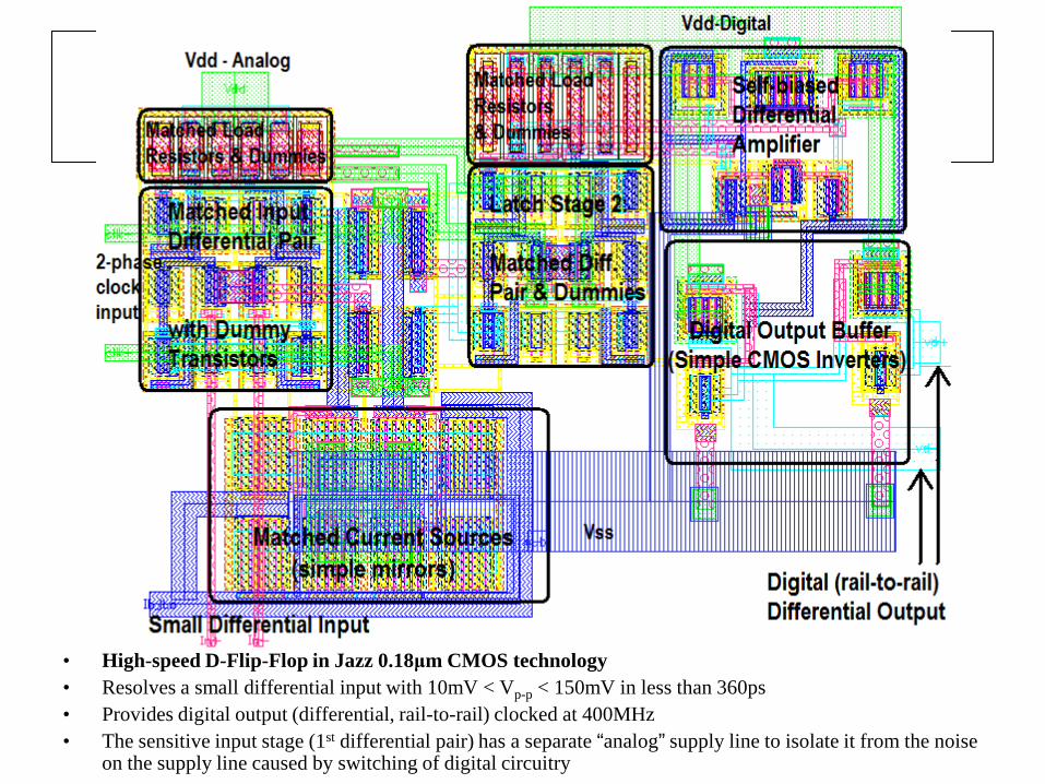
ECEN-474-2009 Jose Silva-Martinez
57
• High-speed D-Flip-Flop in Jazz 0.18μm CMOS technology • Resolves a small differential input with 10mV < Vp-p < 150mV in less than 360ps • Provides digital output (differential, rail-to-rail) clocked at 400MHz • The sensitive input stage (1st differential pair) has a separate “analog” supply line to isolate it from the noise
on the supply line caused by switching of digital circuitry
ECEN-474-2009 Jose Silva-Martinez
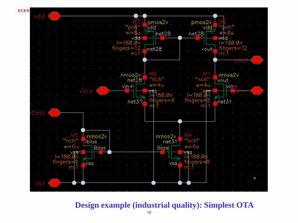
58 Design example (industrial quality): Simplest OTA

ECEN-474-2009 Jose Silva-Martinez
59 Overall amplifier: Have a look on the guard rings and additional well!

ECEN-474-2009 Jose Silva-Martinez
60 BIAS: you may be able to see the dummies, symmetry and S/D connections

ECEN-474-2009 Jose Silva-Martinez
61
From downstairs
Differential pair

ECEN-474-2009 Jose Silva-Martinez
62

ECEN-474-2009 Jose Silva-Martinez
63
Details on the P-type current mirrors

ECEN-474-2009 Jose Silva-Martinez
64
Q-value of Spiral Inductors in CMOS
Process Most of the following slides were taken from
Seminar by: Park, Sang Wook
TAMU, 2003

What is Q?
65
dissipatedpower averagestored energyω≡Q
s
s
RLQ ω
=Simple Inductor Model:
Integrated Spiral Inductor “Pi” Model
ECEN-474-2009 Jose Silva-Martinez
66
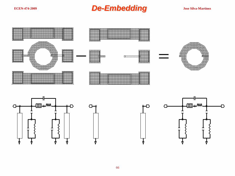
De-Embedding
ECEN-474-2009 Jose Silva-Martinez
67
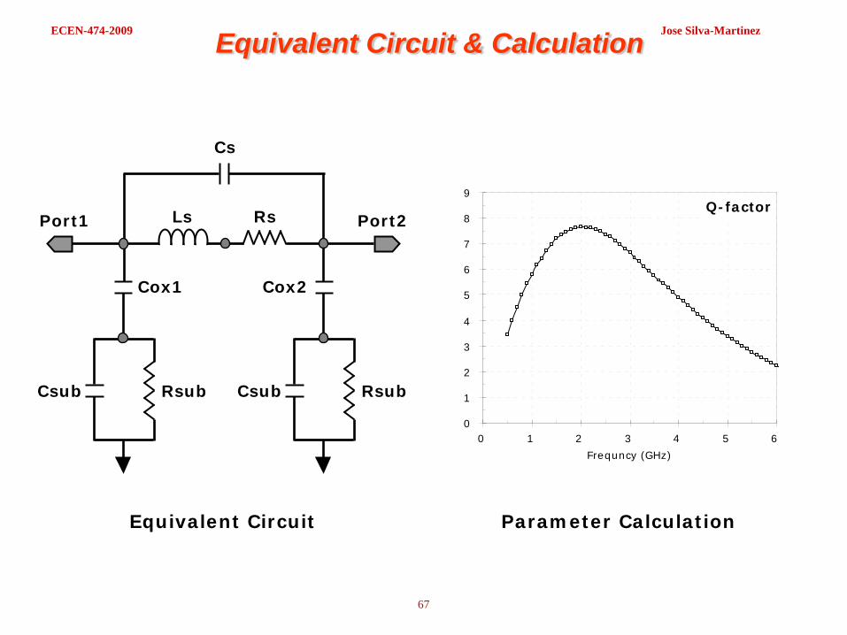
Equivalent Circuit & Calculation
Equivalent Circuit Parameter Calculation
Port1 Port2 Ls Rs
Cs
Cox1
Rsub Csub
Cox2
Rsub Csub
Q-factor
0
1
2
3
4
5
6
7
8
9
0 1 2 3 4 5 6Frequncy (GHz)

ECEN-474-2009 Jose Silva-Martinez
68
Metal-5 under path
W : Width (=14.5um)
S : Space (=1.5um)
R : Radius
Metal-6 (thickness=2um)
N : # of Turns
Layout & Structure
Oxide
Substrate
Via-5
ECEN-474-2009 Jose Silva-Martinez
69
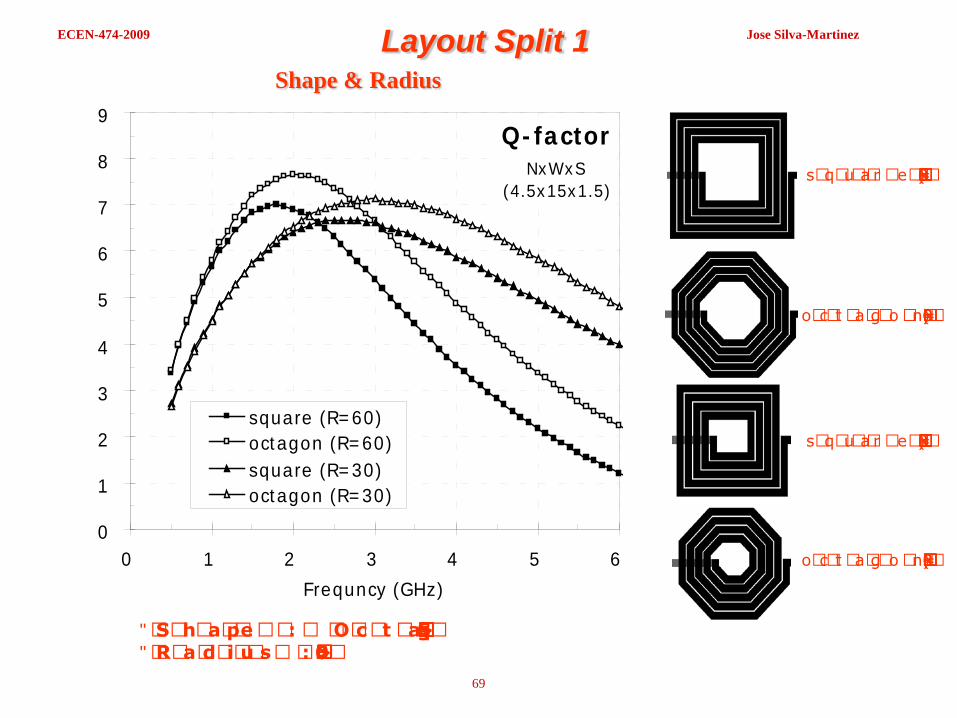
Q-factorNxWxS
(4.5x15x1.5)
0
1
2
3
4
5
6
7
8
9
0 1 2 3 4 5 6Frequncy (GHz)
square (R=60)octagon (R=60)square (R=30)octagon (R=30)
squar e (R=60)
oct ago n (R=60)
squar e (R=30)
oct ago n (R=30)
Shape & Radius
" Shape : Oct agon > Square " Radius : 60 > 30
Layout Split 1

ECEN-474-2009 Jose Silva-Martinez
70
Layout Split 2
Q-factorNxRxWxS
(4.5x60x15x1.5)
0
1
2
3
4
5
6
7
8
9
0 1 2 3 4 5 6Frequncy (GHz)
nonenwellpolymetal1
none
nwell
poly
metal 1
PGS (Patterned Ground Shield) material
PGS : Po ly > Nwell > none > Metal1

ECEN-474-2009 Jose Silva-Martinez
71
Layout Split 3
none
poly PGS(wide)
GS (Ground Shield) type
Q-factor

ECEN-474-2009 Jose Silva-Martinez
72
Layout Split 4 Metal Stack
Q-factorNxRxWxS
(4.5x60x15x1.5)
0
1
2
3
4
5
6
7
8
9
0 1 2 3 4 5 6Frequncy (GHz)
M 6M 5/6M 4/5/6M 3/4/5/6
M 3/ 4/5/6
M 4/5/6
M 5/6
M 6
" St ack : M6 > M5/6 > M4 /5/6 > M3/4/5/6

ECEN-474-2009 Jose Silva-Martinez
73
Chip microphotograph Chip was fabricated in 0.35um CMOS through MOSIS.
Total area 2mm×2mm.
It includes the monolithic PLL, standalone prescaler, loop filter and VCO, etc.
The chip was packaged in 48-pin TPFQ.
1Texas A&M University 2Texas Instruments
Keliu Shu1, Edgar Sánchez-Sinencio1, Jose Silva-Martinez1, and Sherif H. K. Embabi2
Best student paper award: Radio Frequency Intl Conference 2003 IEEE-JSSC-June 2003
Next Time
• Table-Based (gm/ID) Design Examples
74