Embed Size (px)
Citation preview

Sam Palermo Analog & Mixed-Signal Center
Texas A&M University
ECEN474: (Analog) VLSI Circuit Design Fall 2012
Lecture 18: OTA CMFB Examples

Announcements
• No class on Monday • Preliminary report still due Monday (11/19)
• If you are doing anything not on the list, give me a brief description as soon as possible
• We will have class on Wednesday (11/21) • Project Extra Credit
• Potential for 20% extra credit if you layout a key block • Report on Dec. 4 doesn’t have to have layout • For extra credit, an updated report can be turned in during the
presentation time (Dec. 10) with layout results • The post-layout performance is the only thing that will be considered
relative to the original report, i.e. no major circuit changes from the original report
2

Agenda
• Multi-OTA stages CMFB • OTA-C filter w/ CMFB example
3

TAMU-ECEN-474 Jose Silva-Martinez_08
- 4 -
2 IB
IB+icmfb
GND
VC
IB
IB
IB IB
GND
IB
VC
CMFB is required for Differential Structures
CMFB Requirements: Fixes the OTA output (low offset) ==> High dc loop gain Reduction of common-mode noise==> Large Bandwidth
CMFB CMFB
Rg1g
Gm
mm +=
R R mm gG =
GND
CMFB icmfb = gcmfb(v01+v02-Vref)
IB+icmfb IB+icmfb

TAMU-ECEN-474 Jose Silva-Martinez_08
- 5 -
IB
VB1
IB IB
VREF IB
Common-mode loop gain = AV Gmp RL 3 poles in the CMFB loop. Loop stability requires AV Gmp / CL < ωp2 @ VC, ωp3 @ VB1
IB
IB IB
IB
VB2
VDD
VSS
VC
Efficient CMFB for Differential Pair Based OTAs
+ - AV

TAMU-ECEN-474 Jose Silva-Martinez_08
- 6 -
IB IB
Sensitive to supply noise and common-mode input signals
IB
IB IB
IB
VDD
VSS
V1+v1 V2+v2
From CMFB
to next stage
IB
GND
VDD
VSS
From CMFB
to next stage
v2 v1
MC
M1
R1 R1
M1
Pseudo-Differential OTAs with Source Degeneration
Little sensitive to supply noise and Common-mode noise

TAMU-ECEN-474 Jose Silva-Martinez_08
- 7 -
IB
IB IB
IB
CMFB
IB
IB IB
IB
VDD
VSS
IB
GND
M1 M1 R1 R1
M1
Efficient CMFB for Pseudo-Differential OTAs
common-mode detector

TAMU-ECEN-474 Jose Silva-Martinez_08
- 8 -
OTA based on complementary differential pairs
-v1 v1v0 -v0
VCP
VCN
CLCL
M1 M1
M3 M3
M4 M4
M2 M2
VDD
VSS
Efficient OTA based on linear complementary differential pairs
Linear circuit due to source degeneration M3 and M4
Suitable for fast applications
11 22
2
31
1
++
+=
Mm
m
Mm
mm Rg
gRggG

TAMU-ECEN-474 Jose Silva-Martinez_08
- 9 -
Filter is based on Biquadratic Cells: Biquad Realization in Gm-C topology
!!! Fast CMFB is required
vi-
vi+
vo-
vo++ -
- +
+ -
- +
+ -
- +
+ -
- +
gm1 gm2 gm1
2C2
2C2
2C1
2C1
gm1
f0 (MHz) Gm1 (mA/V)
Gm2 (mA/V)
Biquad 1 537.6 5.4 9.6 Biquad 2 793.2 5.4 5.07

TAMU-ECEN-474 Jose Silva-Martinez_08
- 10 -
Time Domain characterization of the CMFB Common-mode characterization using common-mode current pulses One CMFB circuit per pole •Pulse response of the
CMFB •Phase margin is better than 45 degrees
CMFB
icm
icm
vi-
vi+
vo-
vo++ -
- +
+ -
- +
+ -
- +
+ -
- +
CMFB

TAMU-ECEN-474 Jose Silva-Martinez_08
- 11 -
-v1VREF
Previous OTA CMFB Next OTA
v1
A B
C
DE
v03 v04v01 v02
OTA with Class AB Common-mode Feedback
• Common-mode signal is detected at next stage • Class AB error amplifier is used • 5 non-dominant poles at A~E • 2 LHP zeros at A and C (Helpful in BW extension)
• Most important non-dominant pole at D
TAMU-ECEN-474 Jose Silva-Martinez_08
- 12 -
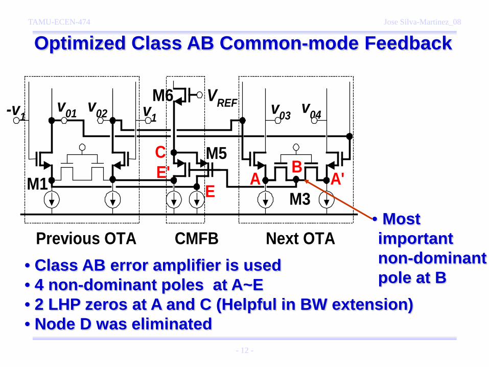
Optimized Class AB Common-mode Feedback
• Most important non-dominant pole at B
v03 v04-v1 v1v01 v02
VREF
Previous OTA CMFB Next OTA
A A'B
C
M1M3
M6
M5E'
E
• Class AB error amplifier is used • 4 non-dominant poles at A~E • 2 LHP zeros at A and C (Helpful in BW extension) • Node D was eliminated

TAMU-ECEN-474 Jose Silva-Martinez_08
- 13 -
+
+
+
+
≅
1m
D
03
B
L
L
L6m
5m
5m
VCMFB
g
sC1
g
sC1
g
sC1
gg
g21
g
A
Analysis of Class AB Common-mode Feedback
•2 pole-zero pairs (A and C) are very close to each other
•More stable CMFB
CMFB can be simplified taking advantage of circuit’s symmetry

TAMU-ECEN-474 Jose Silva-Martinez_08
- 14 -
Remarks • DC operating points for high impedances are difficult to fix • Fully differential amplifiers with high output impedance nodes must use common-mode feedback circuits . • Common mode circuits can fix the DC operating points as well as minimize the common mode output components. • Low voltage constraints impose optimal bias conditions at both the input and output ports of an amplifier. • Common mode circuits for LV should be used both at the input and output

Next Time
• Analog Applications • OTA-C Filters • Variable-Gain Amplifiers • Switch-Cap Filters, Broadband Amplifiers
• Output Stages • Bandgap Reference Circuits • Distortion
15