Embed Size (px)
Citation preview
Modeling and Fabrication of Piezoelectric
Nanomaterial Devices for Sensing and
Energy Harvesting
A DISSERTATION SUBMITTED TO THE FACULTY OF THE
UNIVERSITY OF MINNESOTA
BY
Kory Jenkins
IN PARTIAL FULFILLMENT OF THE REQUIREMENTS
FOR THE DEGREE OF
DOCTOR OF PHILOSOPHY
Prof. Rusen Yang, Prof. Jürgen Konczak
May 2018

© Kory Jenkins 2018

i
Acknowledgement
I would like to express my deepest gratitude to my advisor, Prof. Rusen Yang, for
his guidance and support throughout my graduate studies, and for introducing me to the
exciting world of nanomaterials. He taught me how to approach and solve challenging
problems, through his ever-present commitment to the success of his students. Although I
still have much to learn, Prof. Yang has given me the tools to pursue this knowledge,
wherever it may lead.
I also extend my great appreciation to my co-advisors, Prof. Jürgen Konczak and
Prof. Martha Flanders. Their support has enabled me to explore rewarding and meaningful
work in haptics and prosthetics. I am grateful to my committee members, Prof. Victor
Barocas and Prof. Rajesh Rajamani, for graciously welcoming me into their wonderful lab
groups during my research rotations. Their advice has been invaluable to this work.
Many thanks must be given to my fellow NSTL lab members, especially Dr. Vu
Nguyen, Dr. Ren Zhu, and Wengui Zhang. Their mentoring, collaboration, and friendship
have been invaluable. I also want to thank NSTL undergraduate members Kayla Bohlke,
Steve Kelly, Alex Jurcoi, Brandon Maas, and Kenny Ostyn Harsono for their many
contributions and collaboration. I am grateful for my collaborations with visiting scholars
Dr. Huimin Hao, Dr. Haiwu Zheng, Dr. Xiaowen Huang, and Dr. Jianlin Chen.
I sincerely thank the faculty, staff, and students in the Mechanical Engineering
department for their support and collaboration. I also thank the NSF IGERT fellowship
program faculty, staff, and students, in particular director Prof. Bin He and program
coordinator Rachel Jorgenson. The IGERT program has broadened my horizons and given
me a sense of community that I will always treasure. This work could not have been
completed without support from faculty and staff in the Minnesota Nano Center, the U of
M Characterization Facility, and the Minnesota Supercomputing Institute.
Last, but certainly not least, thank you to my amazing wife Alyssa, for her constant
support, encouragement, and love over the last five years. And thank you to my family for
their love and encouragement.

ii
Dedication
To
My wife, Alyssa
My mother, Maureen, My father, Mark, and my brother, Kyle
iii
Abstract
Piezoelectric nanomaterials are the basis for many devices including
nanogenerators, force sensors, and strain sensors. Barriers to the continued development
of these devices include a limited understanding of piezoelectric behavior in emerging
nanomaterials, and the limitations of nanomaterial fabrication techniques. This thesis
explores emerging piezoelectric nanomaterial behavior through finite element modeling,
expands a nanomaterial fabrication technique to new substrates, and demonstrates new
piezoelectric nanomaterial devices enabled by these findings.
Diphenylalanine (FF) peptide is an emerging bio-inspired piezoelectric material
with remarkable electromechanical properties. First principles analysis and finite element
models have explored the mechanical properties of FF peptide. However, limited
information is available to predict the piezoelectric performance of FF peptide compared
to conventional piezoelectric nanomaterials. Device fabrication is high risk, requiring
significant investments in infrastructure, funding, and time. Therefore, finite element
models of piezoelectric potential are needed to inform the design of devices based on FF
peptide and other piezoelectric nanomaterials.
In addition to piezoelectricity, nanomaterials such as zinc oxide (ZnO) may have
semiconducting properties, making them suitable for highly sensitive devices enabled by
the piezotronic effect. Chemical vapor deposition (CVD) can produce ultra-long
nanowires, but the high-temperature process is incompatible with flexible polymers and
other low-temperature substrates, limiting device design. Synthesis of emerging 2D
piezoelectric nanomaterials such as molybdenum disulfide (MoS2) can also benefit from
low-temperature substrates. These challenges highlight the need to expand chemical vapor
deposition to low-temperature substrate materials.
First, a finite element model of a single nanowire was used to compare the
piezoelectric potential in FF peptide and conventional piezoelectric materials. A 2D model
of a flexible nanogenerator based on FF peptide microrods was created to predict the device
performance. A flexible FF peptide nanogenerator was fabricated for mechanical energy
harvesting, and the power generation was characterized.
iv
Next, a finite element model was created to investigate a piezotronic force sensor
design for haptics and prosthetics applications. The design, based on beam theory,
consisted of two vertical arrays of ultra-long ZnO nanowires in a polymer matrix. Contact
forces were applied to the model, and the piezopotential in the nanowires was calculated.
The use of ultra-long ZnO nanowires grown by CVD was expanded to a soft polymer
substrate by a mechanical transfer process. A stretchable piezotronic strain sensor was
fabricated, and characterized.
Lastly, an apparatus for using low-temperature growth substrates inside of a high-
temperature CVD furnace was designed and fabricated. The cooling assembly delivered
chilled water to provide localized cooling for substrates inside the furnace. The cooling
assembly was used to synthesize molybdenum disulfide (MoS2) on a low-temperature iron
pyrite (FeS2) substrate in a CVD furnace.
In summary, finite element models predicted that FF peptide could generate
significantly higher voltages than conventional piezoelectric nanomaterials for a given
force. The first flexible piezoelectric FF peptide nanogenerator was fabricated and
characterized, validating the model. A finite element model of a piezotronic force sensor
predicted that the sensor could detect both shear and normal force components, and could
exceed the force sensitivity of human mechanoreceptors. A stretchable piezotronic strain
sensor was fabricated using a mechanical transfer process to expand CVD grown ZnO
nanowires to a soft polymer substrate. The gauge factor of the piezotronic strain sensor
exceeded that of conventional metal strain gauges. An apparatus for cooling substrates
inside a high-temperature CVD furnace was demonstrated for the synthesis of MoS2 on a
low-temperature substrate. The results show that finite element models can successfully
predict piezoelectric behavior in emerging nanomaterials, and inform the design of new
piezoelectric nanomaterial devices. Expanding the high-temperature CVD process to low-
temperature substrates can help to realize new device designs, and benefit the synthesis of
emerging piezoelectric nanomaterials. Devices enabled by piezoelectric nanomaterials can
provide solutions to challenges in sustainable energy and human health.

v
Table of Contents
Acknowledgement ............................................................................................................... i
Dedication ........................................................................................................................... ii
Abstract .............................................................................................................................. iii
List of Tables ..................................................................................................................... vi
List of Figures ................................................................................................................... vii
Chapter 1. Introduction ....................................................................................................... 1
1.1 The piezoelectric effect .................................................................................................... 1
1.2 Piezoelectric nanomaterials.............................................................................................. 4
1.3 The piezotronic effect .................................................................................................... 15
1.4 Review of energy harvesting with piezoelectric nanomaterials ..................................... 16
1.5 Review of strain and force sensing with piezotronic nanomaterials .............................. 28
1.6 Scope of this Thesis ....................................................................................................... 40
Chapter 2. Modeling and fabrication of a flexible piezoelectric nanogenerator with
diphenylalanine peptide .................................................................................................... 42
2.1 Finite element model of a single nanowire .................................................................... 44
2.2 Finite element model of a 2D flexible nanogenerator .................................................... 47
2.3 Fabrication and testing of a flexible nanogenerator ....................................................... 52
2.4 Chapter summary ........................................................................................................... 57
Chapter 3. Modeling and fabrication of piezotronic force and strain sensors .................. 59
3.1 Tactile sensing for haptics and prosthetic limbs ............................................................ 59
3.2 Design and modeling of a piezotronic contact force sensor .......................................... 65
3.3 Design and fabrication of a stretchable piezotronic strain sensor .................................. 70
3.4 Chapter summary ........................................................................................................... 81
Chapter 4. Design of a substrate cooling assembly for CVD systems.............................. 82
4.1 Chemical vapor deposition ............................................................................................ 82
4.2 CVD substrate cooling assembly design ........................................................................ 85
4.3 CVD cooling assembly testing and synthesis of MoS2 on FeS2 substrate ..................... 93
4.4 Chapter summary ........................................................................................................... 96
Chapter 5. Conclusions ..................................................................................................... 97
References ....................................................................................................................... 100
Appendix ......................................................................................................................... 108

vi
List of Tables
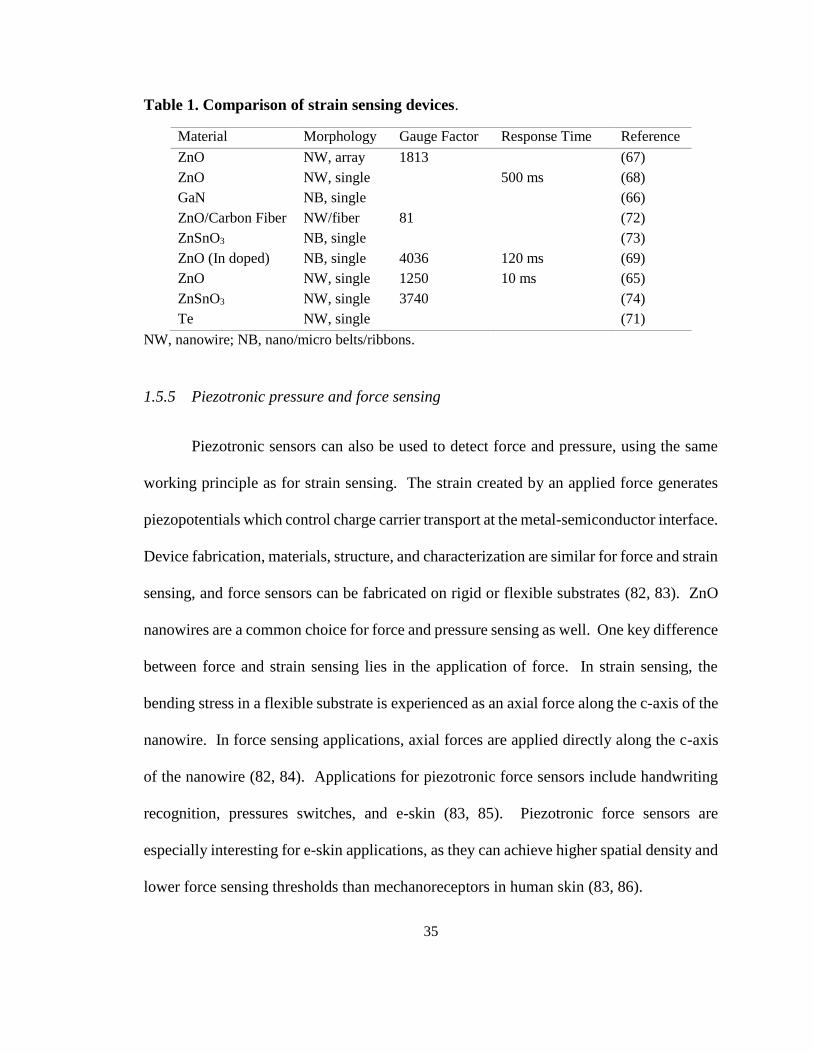
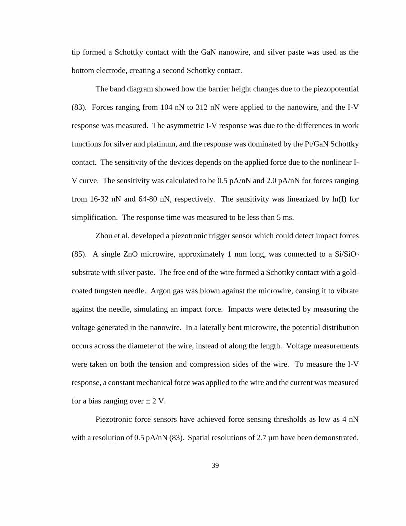
Table 1. Comparison of strain sensing devices ................................................................. 35
Table 2. Comparison of force and pressure sensing devices ............................................ 40
Table 3. Electrical and mechanical properties of FF peptide ............................................ 45
Table 4. Comparison of simulated piezoelectric potentials in a single nanowire under
axial or transverse loading for various materials .............................................................. 47
vii
List of Figures
Figure 1. Uniaxial extension of a cylindrical rod ............................................................... 1
Figure 2. Electric potential in a piezoelectric material under applied displacement .......... 3
Figure 3. Electrostatic potential in ZnO nanowire under axial force .................................. 6
Figure 4. Electrostatic potential in a ZnO nanowire under transverse force ...................... 7
Figure 5. SEM image of monolayer molybdenum disulfide flakes .................................. 11
Figure 6. Van der Waals epitaxy of MoS2 on graphene ................................................... 12
Figure 7. Synthesis of FF peptide microrods .................................................................... 14
Figure 8. Conventional and piezotronic transistors .......................................................... 16
Figure 9. Multilayer nanogenerator based on vertical arrays of ZnO nanowires ............. 20
Figure 10. Lateral microwire nanogenerator for biomechanical energy harvesting ......... 22
Figure 11. Monolayer MoS2 nanogenerator...................................................................... 24
Figure 12. Energy harvesting characteristics of MoS2...................................................... 25
Figure 13. Energy harvesting characteristics of FF peptide ............................................. 27
Figure 14. Single ZnO nanowire piezotronic strain sensor............................................... 33
Figure 15. Piezo-phototronic force sensing with ZnO nanowires .................................... 38
Figure 16. Model of piezoelectric potential in single nanowire ....................................... 46
Figure 17. COMSOL Multiphysics model of 2D FF peptide nanogenerator ................... 49
Figure 18. Stress and strain in 2D model of FF peptide nanogenerator ........................... 50
Figure 19. Microrod electric potential in 2D model of FF peptide nanogenerator ........... 52
Figure 20. Design, fabrication, and testing of FF peptide flexible nanogenerator ........... 55
Figure 21. Characterization of FF peptide flexible nanogenerator ................................... 56
viii
Figure 22. Working principle of piezotronic shear and normal force sensor ................... 66
Figure 23. Simulation of piezopotential in ZnO contact force sensor .............................. 67
Figure 24. Applications for piezotronic contact force sensor ........................................... 69
Figure 25. Piezotronic strain sensor fabrication steps ...................................................... 73
Figure 26. Stretchable and conformal piezotronic strain sensor testing ........................... 75
Figure 27. Mechanical characterization of stretchable strain sensor ................................ 76
Figure 28. Electrical characterization of stretchable piezotronic strain sensor ................ 77
Figure 29. ZZ component of strain tensor for a stepped shaft under applied displacements
........................................................................................................................................... 78
Figure 30. Major components and operation of a CVD tube furnace ............................... 84
Figure 31. Temperature profile in a CVD tube furnace .................................................... 85
Figure 32. Major components of CVD cooling assembly ................................................ 87
Figure 33. Detailed view of sample cooling chamber ...................................................... 89
Figure 34. Detailed view of insulating sleeve assembly ................................................... 90
Figure 35. Detailed view of cooling assembly endcap ..................................................... 91
Figure 36. Fabricated cooling assembly ........................................................................... 92
Figure 37. Cutaway views of cooling assembly ............................................................... 92
Figure 38. Cross-section view of cooling assembly in tube furnace ................................ 93
Figure 39. Schematic of MoS2 growth in tube furnace with CVD cooling assembly ...... 94
Figure 40. Sample of iron pyrite (FeS2) substrate material .............................................. 95
Figure 41. SEM image of MoS2 structures grown on FeS2 substrate with CVD cooling
assembly ............................................................................................................................ 95
ix
Figure A1. Detailed view of stress, strain, and piezopotential in a single FF peptide
microrod at location x = 11 mm (Region I) .................................................................... 108
Figure A2. Detailed view of stress, strain, and piezopotential in a single FF peptide
microrod at location x = 15 mm (Region II) ................................................................... 109
Figure A3. Microfabrication steps for piezotronic contact force sensor ........................ 110
Figure A4. Testing fabricated piezotronic contact force sensors .................................... 110
1
Chapter 1. Introduction
1.1 The piezoelectric effect
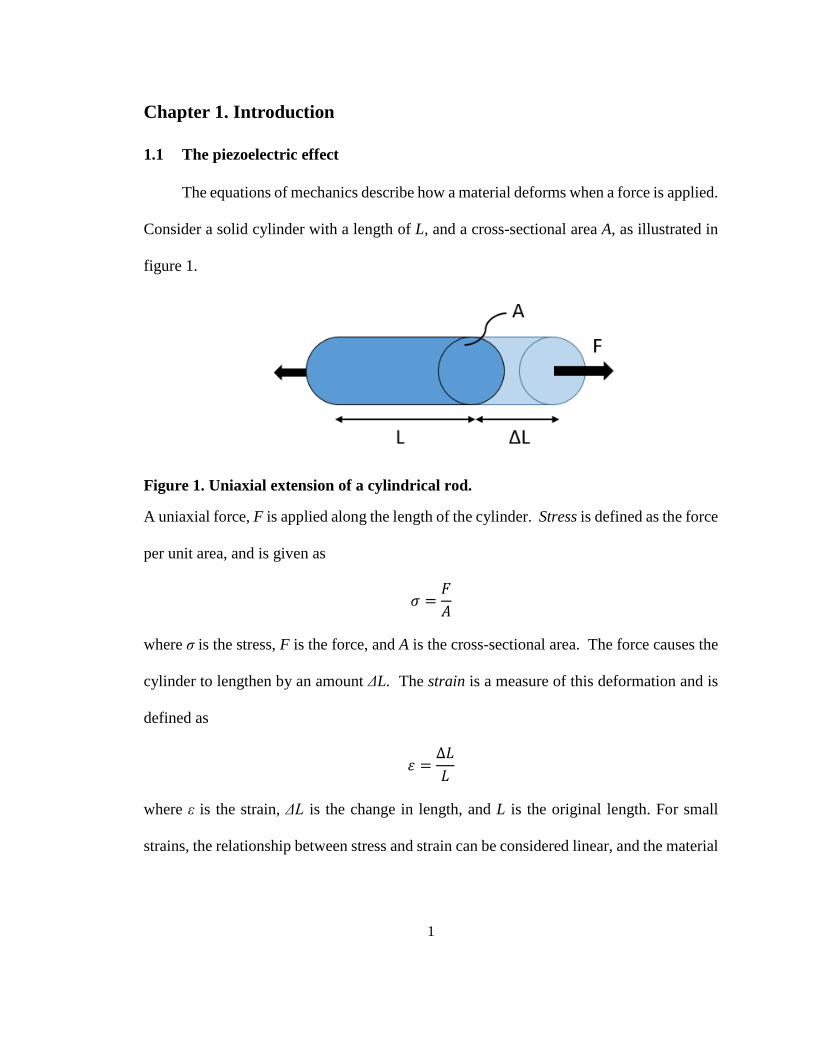
The equations of mechanics describe how a material deforms when a force is applied.
Consider a solid cylinder with a length of L, and a cross-sectional area A, as illustrated in
figure 1.
Figure 1. Uniaxial extension of a cylindrical rod.
A uniaxial force, F is applied along the length of the cylinder. Stress is defined as the force
per unit area, and is given as
𝜎 =𝐹
𝐴
where σ is the stress, F is the force, and A is the cross-sectional area. The force causes the
cylinder to lengthen by an amount ΔL. The strain is a measure of this deformation and is
defined as
𝜀 =∆𝐿
𝐿
where ε is the strain, ΔL is the change in length, and L is the original length. For small
strains, the relationship between stress and strain can be considered linear, and the material
2
is said to be linear elastic. For a linear elastic material, the relationship between stress and
strain is given as
𝜎 = 𝐸𝜀
where E is the modulus of elasticity, also called Young’s modulus. The elastic modulus
relates the applied stress to the deformation of the material. The equations above hold for
uniaxial loading, and may be expanded upon to account for more complex loading
conditions, and direction-dependent material properties.
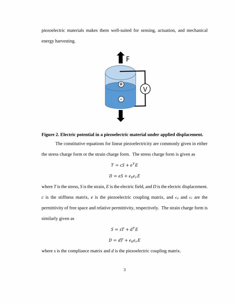
Piezoelectricity is a property of crystalline materials with non-central symmetry.
In non-centrosymmetric crystals, a mechanical stress or strain creates (or changes) a net
displacement between the center of positive charge, and the center of negative charge. This
creates an electric dipole moment, and induces charge polarization. The result is an
electrical voltage in the material, as seen in figure 2. A converse piezoelectric effect also
exists, in which an applied voltage induces strain in a piezoelectric material. There are 21
classes of crystals which possess non-central symmetry. The cubic class 432 is an
exception, due to charge cancellation along the <111> axis. Piezoelectricity can be found
in semiconductors including zinc oxide (ZnO), polymers such as poly(vinylidene fluoride-
trifluoroethylene) (PVDF-TRFE), single atomic layer materials such as molybdenum
disulfide (MoS2), and in certain biological and bio-inspired materials including dry
collagen, and diphenylalanine (FF) peptide microstructures (1-3). Among conventional
piezoelectric materials, ceramics such as lead zirconate titanate (PZT) and barium titanate
(BaTiO3) are the most well-known. The inherent electromechanical coupling in
3
piezoelectric materials makes them well-suited for sensing, actuation, and mechanical
energy harvesting.
Figure 2. Electric potential in a piezoelectric material under applied displacement.
The constitutive equations for linear piezoelectricity are commonly given in either
the stress charge form or the strain charge form. The stress charge form is given as
𝑇 = 𝑐𝑆 + 𝑒𝑇𝐸
𝐷 = 𝑒𝑆 + 𝜖0𝜖𝑟𝐸
where T is the stress, S is the strain, E is the electric field, and D is the electric displacement.
c is the stiffness matrix, e is the piezoelectric coupling matrix, and ϵo and ϵr are the
permittivity of free space and relative permittivity, respectively. The strain charge form is
similarly given as
𝑆 = 𝑠𝑇 + 𝑑𝑇𝐸
𝐷 = 𝑑𝑇 + 𝜖0𝜖𝑟𝐸
where s is the compliance matrix and d is the piezoelectric coupling matrix.
4
The quantities that describe piezoelectric materials in the preceding equations are
tensors with rank of either 4, 3, or 2. However there can be significant symmetries due to
the physical crystal structures of piezoelectric materials.
In addition to electromechanical coupling, piezoelectric materials may also possess
semiconducting properties. Semiconductors have electrical conductivity somewhere
between insulators and metals, and are the basis for transistors and many electrical devices.
Silicon is perhaps the most well-known among non-piezoelectric semiconductors.
Examples of piezoelectric semiconductors include zinc oxide (ZnO), gallium nitride
(GaN), and molybdenum disulfide (MoS2).
1.2 Piezoelectric nanomaterials
Nanomaterials are defined as any material structure with a length scale on the order
of 10-9 meters. Nanomaterials have many advantages over bulk materials due to their
favorable scaling laws (4, 5). Nanomaterials often exist as quasi-2D or 1D structures such
as monolayer materials and nanowires. Nanomaterials may have different properties from
their bulk counterparts, and can play an important role in sensing and energy harvesting.
Less material is required to produce nanomaterials, and material synthesis is often highly
scalable (6). Nanomaterials have favorable scaling laws, and can have improved
piezoelectric properties not seen in bulk materials. Certain semiconducting materials, such
as MoS2, may even switch from an indirect to direct bandgap at the nanoscale (3, 4, 7).
The elastic modulus of ZnO nanowires is higher than that of bulk ZnO, and their single
crystal nature is resistant to fatigue. (8, 9).

5
1.2.1 Zinc Oxide
Zinc oxide is a piezoelectric material which exists in 3 distinct crystal structures,
zinc blende (sphalerite), rock salt, and wurtzite (10). Although all ZnO crystal structures
are piezoelectric, the hexagonal wurtzite structure has been most heavily researched for
sensing and energy harvesting applications (11, 12). Zinc oxide can be grown to form
nanowires, which are high aspect ratio, quais-1D structures that can develop large
piezopotentials. ZnO is a direct bandgap semiconductor with a wide bandgap of 3.37 eV
(13). ZnO has an electron affinity of 4.2 eV, allowing it to form Schottky contacts with
high work function metals such as gold and platinum. Brillson and Lu have
comprehensively reviewed the formation of Schottky and Ohmic contacts with ZnO (14).
The favorable scaling properties of nanomaterials are illustrated by the enhanced
mechanical properties of ZnO nanowires. Using transmission electron microscopy (TEM),
Agrawal and colleagues measured the elastic modulus of ZnO nanowires (9). The elastic
modulus of the ZnO nanowires increased from 140 GPa to 160 GPa as the diameter
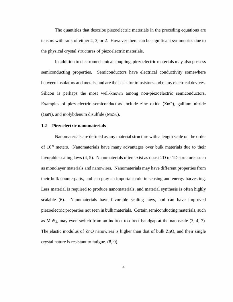
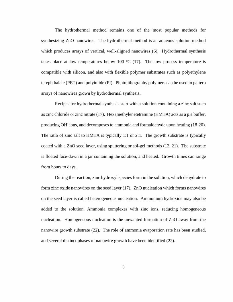
decreased from 80 nm to 20 nm. Gao et al. studied the piezopotential in a ZnO nanowire
using finite element methods (15). The authors applied an axial load of 85 nN to a 1200
nm long nanowire model (figure 3a), and calculated a potential of 0.4 V along the c-axis
of the nanowire as seen in figure 3b and figure 3c. When a pure torsional load was applied
to the nanowire, no net potential was generated along the length of the wire, only small
local potential gradients as seen in figure 3d. Tension or compression loads combined with
torsion produced potentials similar to the pure axial load cases as shown in figure 3e and
6
figure 3f. These results suggest that the most significant piezoelectric potential is produced
by strain in the c-axis, along the length of the nanowire.
Figure 3. Electrostatic potential in ZnO nanowire under axial force. (a) Finite element
model of a ZnO nanowire, length 1200 nm. Arrow indicates c-direction along the length of
the wire. (b) Piezoelectric potential in the ZnO nanowire under 85 nN tensile force and (c)
85 nN compressive force. (d) Piezoelectric potential under a 60 nN twisting force pair. (e)
Piezoelectric potential under simultaneous twisting and tension and (f) simultaneous
twisting and compression. Reprinted from (15) with the permission of AIP publishing.
Copyright 2009.
7
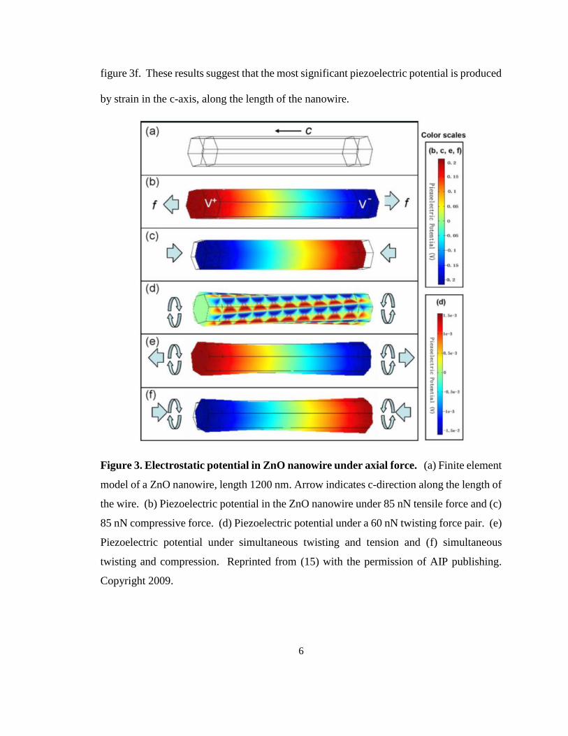
Gao and Wang similarly investigated the potential in laterally bent nanowires using
finite element methods (16). The authors applied an 80 nN transverse load to the tip of the
nanowire model, which resulted in a potential of about ± 0.3 volts across the diameter of
the wire as seen in figure 4a and figure 4b. The analytical solution is shown in figure 4c,
and is compared to the finite element model in figure 4d. ZnO nanogenerators have been
developed to make use of the piezoelectric potential from both axial and transverse
nanowire deflections.
Figure 4. Electrostatic potential in a ZnO nanowire under transverse force. (a) Finite
element model of piezoelectric potential in a ZnO nanowire under 80 nN transverse force.
The nanowire has a length of 600 nm and a diameter of 50 nm. (b) Cross-sectional view
of the nanowire in (a). (c) Analytical solution to piezoelectric potential in the cross-section
of the nanowire. (d) Comparison between potential predicted by finite element model and
analytical solution. Reprinted with permission from (16). Copyright 2007 American
Chemical Society.
8
The hydrothermal method remains one of the most popular methods for
synthesizing ZnO nanowires. The hydrothermal method is an aqueous solution method
which produces arrays of vertical, well-aligned nanowires (6). Hydrothermal synthesis
takes place at low temperatures below 100 ⁰C (17). The low process temperature is
compatible with silicon, and also with flexible polymer substrates such as polyethylene
terephthalate (PET) and polyimide (PI). Photolithography polymers can be used to pattern
arrays of nanowires grown by hydrothermal synthesis.
Recipes for hydrothermal synthesis start with a solution containing a zinc salt such
as zinc chloride or zinc nitrate (17). Hexamethylenetetramine (HMTA) acts as a pH buffer,
producing OH- ions, and decomposes to ammonia and formaldehyde upon heating (18-20).
The ratio of zinc salt to HMTA is typically 1:1 or 2:1. The growth substrate is typically
coated with a ZnO seed layer, using sputtering or sol-gel methods (12, 21). The substrate
is floated face-down in a jar containing the solution, and heated. Growth times can range
from hours to days.
During the reaction, zinc hydroxyl species form in the solution, which dehydrate to
form zinc oxide nanowires on the seed layer (17). ZnO nucleation which forms nanowires
on the seed layer is called heterogeneous nucleation. Ammonium hydroxide may also be
added to the solution. Ammonia complexes with zinc ions, reducing homogeneous
nucleation. Homogeneous nucleation is the unwanted formation of ZnO away from the
nanowire growth substrate (22). The role of ammonia evaporation rate has been studied,
and several distinct phases of nanowire growth have been identified (22).
9
The hydrothermal method produces nanowires with lengths from a few to tens of
microns. Many techniques have been studied to increase nanowire length and reduce
growth time, including microwave and laser assisted growth (22, 23). The hydrothermal
method is popular due to its low temperature, low cost, and scalability. It is compatible
with many substrate materials, making it well-suited for device fabrication.
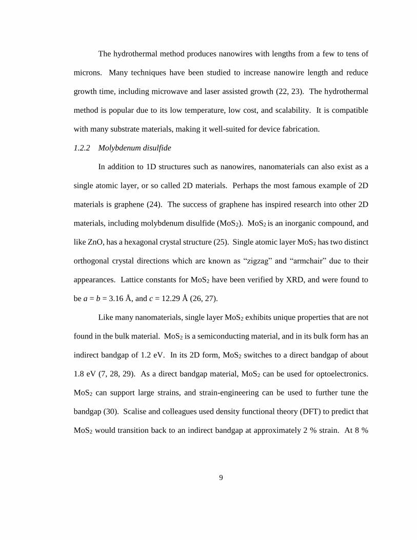
1.2.2 Molybdenum disulfide
In addition to 1D structures such as nanowires, nanomaterials can also exist as a
single atomic layer, or so called 2D materials. Perhaps the most famous example of 2D
materials is graphene (24). The success of graphene has inspired research into other 2D
materials, including molybdenum disulfide (MoS2). MoS2 is an inorganic compound, and
like ZnO, has a hexagonal crystal structure (25). Single atomic layer MoS2 has two distinct
orthogonal crystal directions which are known as “zigzag” and “armchair” due to their
appearances. Lattice constants for MoS2 have been verified by XRD, and were found to
be a = b = 3.16 Å, and c = 12.29 Å (26, 27).
Like many nanomaterials, single layer MoS2 exhibits unique properties that are not
found in the bulk material. MoS2 is a semiconducting material, and in its bulk form has an
indirect bandgap of 1.2 eV. In its 2D form, MoS2 switches to a direct bandgap of about
1.8 eV (7, 28, 29). As a direct bandgap material, MoS2 can be used for optoelectronics.
MoS2 can support large strains, and strain-engineering can be used to further tune the
bandgap (30). Scalise and colleagues used density functional theory (DFT) to predict that
MoS2 would transition back to an indirect bandgap at approximately 2 % strain. At 8 %
10
strain, the material was predicted to exhibit metallic behavior. The elastic modulus of
MoS2 was calculated to be 435 GPa (31).
Monolayer MoS2, like graphene, can be synthesized by mechanical exfoliation (7).
Chemical vapor deposition can also be used to grow monolayer MoS2, either directly from
MoS2 powder, or by sulfurization of molybdenum trioxide (MoO3) (32, 33). Si/SiO2 is
typically used as a growth substrate. Piranha solution is often used as substrate cleanliness
can affect growth (27). CVD produces single crystal, equilateral triangle shapes as seen in
figure 5. The thickness of single atomic layer MoS2 is approximately 0.7 nm (32).
Nucleation of MoS2 crystals occurs preferentially near cracks and other surface
imperfections, and can be controlled by surface modification techniques. Large area
growth of monolayer MoS2 from triangular grains remains challenging. Najamei and
colleagues identified two mechanisms for grain boundary formation, chemical bonding
between in-plane grains, and the overlapping of adjacent grains (32).
11
Figure 5. SEM image of monolayer molybdenum disulfide flakes. MoS2 monolayer
flakes form in a characteristic equilateral triangle morphology. Flakes were grown on
Si/SiO2 substrate. Reprinted with permission from (33). Copyright 2013 American
Chemical Society.
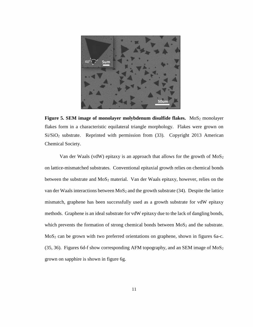
Van der Waals (vdW) epitaxy is an approach that allows for the growth of MoS2
on lattice-mismatched substrates. Conventional epitaxial growth relies on chemical bonds
between the substrate and MoS2 material. Van der Waals epitaxy, however, relies on the
van der Waals interactions between MoS2 and the growth substrate (34). Despite the lattice
mismatch, graphene has been successfully used as a growth substrate for vdW epitaxy
methods. Graphene is an ideal substrate for vdW epitaxy due to the lack of dangling bonds,
which prevents the formation of strong chemical bonds between MoS2 and the substrate.
MoS2 can be grown with two preferred orientations on graphene, shown in figures 6a-c.
(35, 36). Figures 6d-f show corresponding AFM topography, and an SEM image of MoS2
grown on sapphire is shown in figure 6g.
12
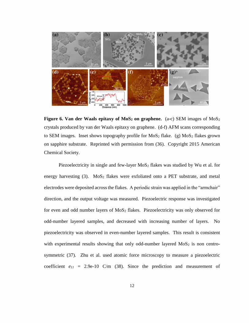
Figure 6. Van der Waals epitaxy of MoS2 on graphene. (a-c) SEM images of MoS2
crystals produced by van der Waals epitaxy on graphene. (d-f) AFM scans corresponding
to SEM images. Inset shows topography profile for MoS2 flake. (g) MoS2 flakes grown
on sapphire substrate. Reprinted with permission from (36). Copyright 2015 American
Chemical Society.
Piezoelectricity in single and few-layer MoS2 flakes was studied by Wu et al. for
energy harvesting (3). MoS2 flakes were exfoliated onto a PET substrate, and metal
electrodes were deposited across the flakes. A periodic strain was applied in the “armchair”
direction, and the output voltage was measured. Piezoelectric response was investigated
for even and odd number layers of MoS2 flakes. Piezoelectricity was only observed for
odd-number layered samples, and decreased with increasing number of layers. No
piezoelectricity was observed in even-number layered samples. This result is consistent
with experimental results showing that only odd-number layered MoS2 is non centro-
symmetric (37). Zhu et al. used atomic force microscopy to measure a piezoelectric
coefficient e11 = 2.9e-10 C/m (38). Since the prediction and measurement of
13
piezoelectricity in single layer MoS2, there has been much work on its synthesis and
characterization. MoS2 has great potential for many piezoelectric applications such as
energy harvesting.
1.2.3 Diphenylalanine peptide
One promising approach to bio-inspired piezoelectric materials are peptides.
Peptides are defined as any chain of two or more amino acids. Dipeptide molecules based
on diphenylalanine can self-assemble into nanotubes, hydrogels, and other structures (39-
42). The nanotube structure of self-assembled FF peptide has potential applications for
drug delivery (43). FF peptide is also known for its role as the core recognition motif for
Alzheimer’s beta amyloid fibrils, leading to growing interest in the study of its self-
assembly and material properties (5).
Self-assembled FF peptide nanotubes and microrods have a hexagonal structure and
demonstrate piezoelectricity, which can be improved by poling (44). Piezoelectricity is
relatively rare among biomaterials, with dry collagen being a notable example (45). The
properties of self-assembled FF peptide structures are impressive among biomaterials.
Experimental measurements for elastic modulus range from 19-27 GPa, and the origin of
this high stiffness has been explored through diffusion tensor theory (46-48). Values up to
18 pm/V have been achieved for the piezoelectric coefficient d33 by poling the material
during growth under an electric field (49, 50).
14
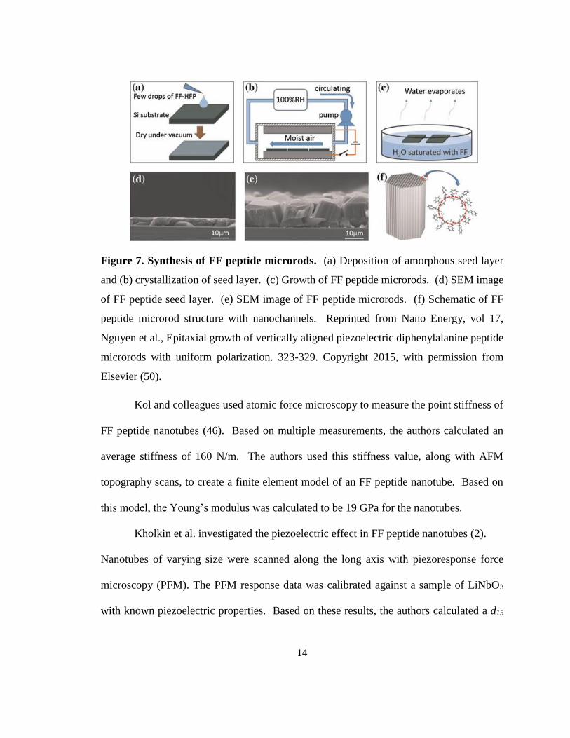
Figure 7. Synthesis of FF peptide microrods. (a) Deposition of amorphous seed layer
and (b) crystallization of seed layer. (c) Growth of FF peptide microrods. (d) SEM image
of FF peptide seed layer. (e) SEM image of FF peptide microrods. (f) Schematic of FF
peptide microrod structure with nanochannels. Reprinted from Nano Energy, vol 17,
Nguyen et al., Epitaxial growth of vertically aligned piezoelectric diphenylalanine peptide
microrods with uniform polarization. 323-329. Copyright 2015, with permission from
Elsevier (50).
Kol and colleagues used atomic force microscopy to measure the point stiffness of
FF peptide nanotubes (46). Based on multiple measurements, the authors calculated an
average stiffness of 160 N/m. The authors used this stiffness value, along with AFM
topography scans, to create a finite element model of an FF peptide nanotube. Based on
this model, the Young’s modulus was calculated to be 19 GPa for the nanotubes.
Kholkin et al. investigated the piezoelectric effect in FF peptide nanotubes (2).
Nanotubes of varying size were scanned along the long axis with piezoresponse force
microscopy (PFM). The PFM response data was calibrated against a sample of LiNbO3
with known piezoelectric properties. Based on these results, the authors calculated a d15
15
piezoelectric coefficient of 60 pm/V. The piezoelectric effect in FF peptide nanotubes is
temperature dependent, and was studied by Heredia et al. Piezoelectricity in FF peptide
was found to decrease as the temperature increased, and was completely lost at 140 ⁰C, due
to a crystalline phase transition (51).
Diphenylalanine peptide structures are commonly synthesized by solution-based
self-assembly (52-55). Nguyen et al. developed a process for epitaxial growth of vertically
aligned FF peptide microrods (50). Figure 7 details the FF peptide synthesis process
including formation of the amorphous seed layer in figure 7a, seed layer crystallization in
figure 7b, and growth of FF peptide microrods in figure 7c. SEM images of the crystallized
seed layer and FF microrods are shown in figure 7d and figure 7e respectively, and a
drawing of the hexagonal microrod structure is given in figure 7f.
1.3 The piezotronic effect
The piezotronic effect was first realized in 2006 by Z.L. Wang’s group (56). The
foundation of the piezotronic effect is the metal-semiconductor heterojunction, or the
interface between a metal and a semiconductor. The semiconductor material is also a
piezoelectric material, which develops an electric potential in response to strain. This
piezoelectric potential in the semiconductor modifies the barrier height and controls
conductivity at the metal-semiconductor interface. This is called the piezotronic effect.
A typical piezotronic device consists of a metal-semiconductor-metal structure.
The metal layers serve as the electrodes, and a bias voltage is applied across the device,
resulting in the flow of current. The metal-semiconductor interface typically uses a high
work function metal such as gold, which can create a Schottky contact, resulting in
16
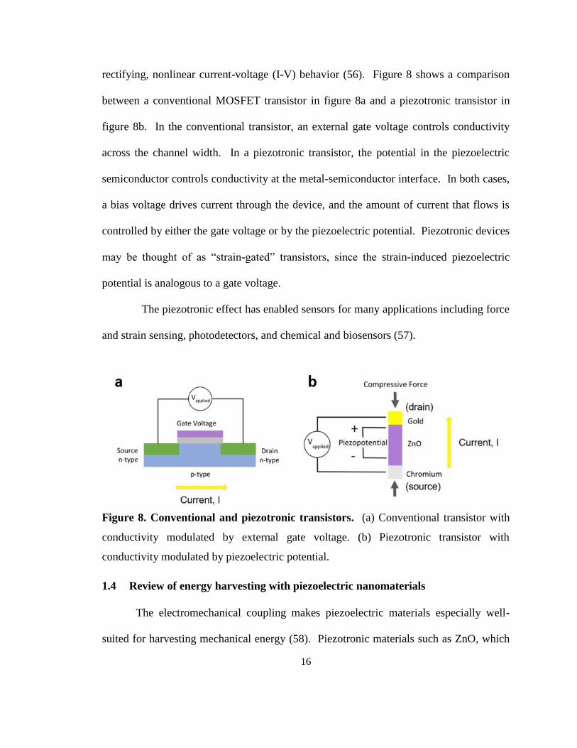
rectifying, nonlinear current-voltage (I-V) behavior (56). Figure 8 shows a comparison
between a conventional MOSFET transistor in figure 8a and a piezotronic transistor in
figure 8b. In the conventional transistor, an external gate voltage controls conductivity
across the channel width. In a piezotronic transistor, the potential in the piezoelectric
semiconductor controls conductivity at the metal-semiconductor interface. In both cases,
a bias voltage drives current through the device, and the amount of current that flows is
controlled by either the gate voltage or by the piezoelectric potential. Piezotronic devices
may be thought of as “strain-gated” transistors, since the strain-induced piezoelectric
potential is analogous to a gate voltage.
The piezotronic effect has enabled sensors for many applications including force
and strain sensing, photodetectors, and chemical and biosensors (57).
Figure 8. Conventional and piezotronic transistors. (a) Conventional transistor with
conductivity modulated by external gate voltage. (b) Piezotronic transistor with
conductivity modulated by piezoelectric potential.
1.4 Review of energy harvesting with piezoelectric nanomaterials
The electromechanical coupling makes piezoelectric materials especially well-
suited for harvesting mechanical energy (58). Piezotronic materials such as ZnO, which
17
have piezoelectric and semiconducting properties, have played an important role in the
development of nanoscale energy harvesting devices (59). MEMS devices and nanoscale
systems present new opportunities and challenges for nanoscale power generation.
Applications include wearables, implantable medical devices, remote structural health
monitoring, and other self-powered systems. Nanogenerator performance has been
steadily improving, and emerging materials are opening new avenues for research.
Piezoelectric nanomaterials are uniquely suited to collect previously neglected sources of
energy, such as biomechanical energy and low intensity vibrations in the environment (60).
1.4.1 Review of energy harvesting with zinc oxide
In 2006, Wang’s group presented the first demonstration of energy harvesting with
piezoelectric ZnO nanowires (60). Using an array of vertical ZnO nanowires, the authors
converted mechanical energy from an atomic force microscope (AFM) into electrical
energy. ZnO nanowires were grown on an Al2O3 substrate by a vapor-liquid-solid (VLS)
method. The reaction was catalyzed with gold, resulting in a gold nanoparticle on the tip
of each nanowire. Individual nanowires were scanned by AFM in contact mode, with a
force of 5 nN. Silver paste formed an Ohmic contact at the bottom of the nanowire, and
the platinum-coated AFM tip formed a Schottky contact with the top of the nanowire. The
output voltage was measured across an external load resistance, and reached 6-9 mV. By
using the AFM topography scan, the authors could estimate the deflection of individual
nanowires. By comparing the elastic energy needed to deform the wires with the
piezoelectric output, an efficiency of 17-30 % was calculated. The piezopotential in a
laterally bent ZnO nanowire develops across the diameter of the nanowire, as seen
18
previously in figure 4. The nanowire develops a positive potential on the tensile side, and
a negative potential on the compressed side. In cases where the gold nanoparticle remained
on top of the nanowire, the piezopotential was neutralized by free carriers and no output
was measured. For many nanowires, the gold nanoparticle fell off of the nanowire tip. In
this case, when the AFM tip scanned across the tip of the nanowire, it formed either a
forward or reversed-biased Schottky contact, depending on the potential in the nanowire.
Therefore, both the piezoelectric and semiconducting properties of the nanowire
contributed to the power generation. The authors calculated an output power density of 10
pW·µm-2, demonstrating the energy harvesting ability of ZnO nanowires.
A standalone nanogenerator was developed using arrays of 1 µm long ZnO
nanowires on gallium nitride (GaN) and sapphire substrates (11). A silicon wafer was
patterned with an array of triangular pyramids and coated with platinum, to form the top
electrode. This top electrode was placed on top of the nanowire array, and connected with
polymer strips. In effect, this created an array of ZnO nanowires, each with their own AFM
tip. The resulting nanogenerator had an area of 2 mm2. The nanogenerator was driven by
ultrasonic waves at a frequency of 41 kHz. The relative motion of the platinum-coated
pyramids and the ZnO nanowires caused some nanowires to deflect laterally, creating
piezoelectric potential. When the pyramids contacted the tensile side of the nanowire, the
reverse-biased Schottky contact caused charge buildup. As the motion between the
pyramids and nanowires continued, the pyramids moved to the compressive side of the
nanowires, creating a forward-biased Schottky contact and discharging. The net effect of
multiple charging and discharging Schottky contacts was a mostly constant DC output
19
voltage. The output voltage was measured to be about 7 mV, and output currents were at
the nA scale. The power output of the nanogenerator was estimated to be 10 µW·cm-2.
The concept of a nanogenerator based on vertical arrays of ZnO nanowires was
expanded by stacking multiple devices together (12). Using silicon substrates with a
sputtered ZnO seed layer, Xu and colleagues grew ZnO nanostructures on each side of the
substrate. On one side, long ZnO nanowires were formed. On the other side, short, conical
ZnO nanotips were grown. The nanotips were coated with a thin layer of gold, and formed
a structure similar to the AFM tip or pyramids in the previous works. Like platinum, gold
can also form a Schottky contact with ZnO nanowires. Multiple silicon substrates were
stacked together so that the nanowires on one layer were in contact with the nanotips on
the layer above as seen in figure 9. Figures 9a-f detail the nanogenerator fabrication
process, and SEM images of the ZnO nanowires and nanotips are shown in figure 9g and
figure 9h, respectively. The stacked nanogenerator was subjected again to ultrasonic
vibrations. As with the single layer design, the Schottky contact switched from reverse-
biased to forward-biased as the nanotips moved across the nanowire. The sum of
contributions from all nanowire/nanotip pairs resulted in a relatively stable DC output. The
stacked nanogenerator architecture produced higher outputs than a single layer
nanogenerator. Output current was measured to be 10 nA and 13 nA for two individual
nanogenerators, and increased to 22 nA when they were connected in parallel. An
antiparallel configuration reduced the combined output to 3 nA. When connected in series,
two nanogenerators produced 3.5 mV compared to 2.6 mV and 0.8 mV individually. By
connecting 4 nanogenerators, the authors produced an output voltage of 62 mV and an
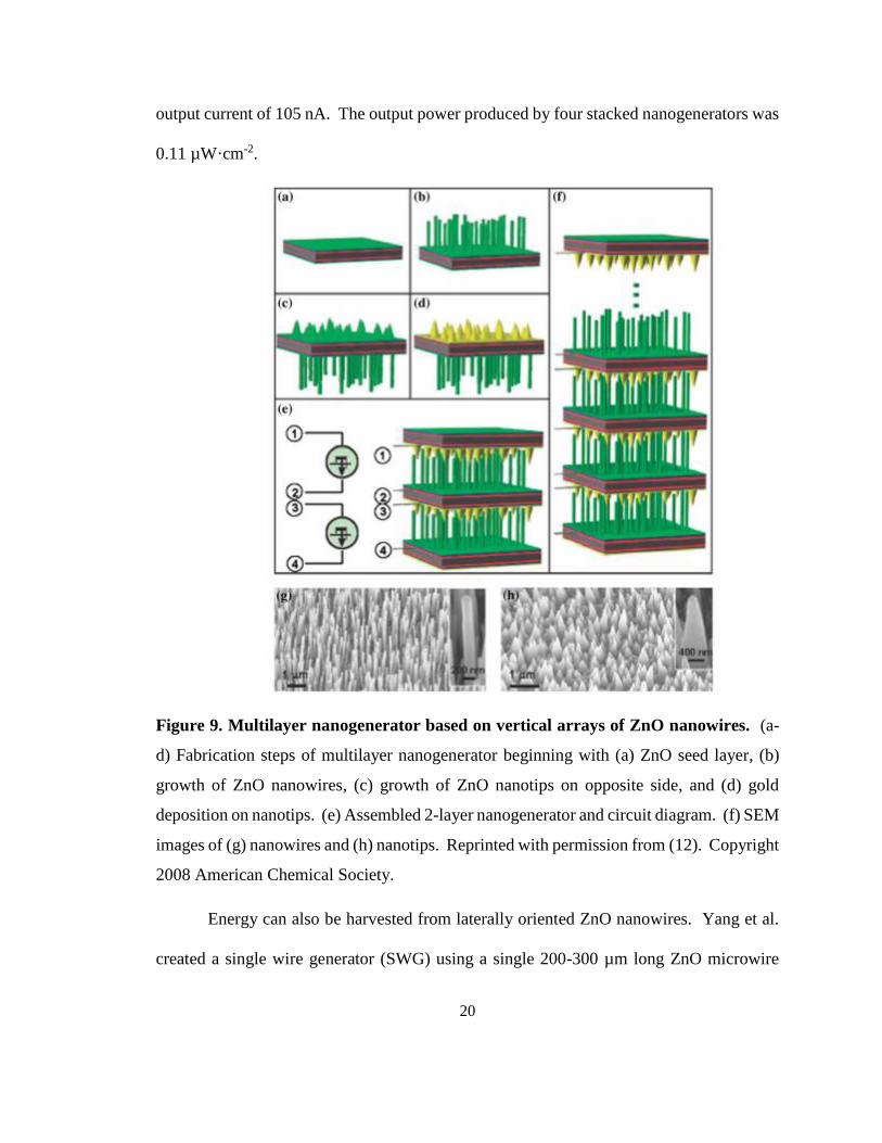
20
output current of 105 nA. The output power produced by four stacked nanogenerators was
0.11 µW·cm-2.
Figure 9. Multilayer nanogenerator based on vertical arrays of ZnO nanowires. (a-
d) Fabrication steps of multilayer nanogenerator beginning with (a) ZnO seed layer, (b)
growth of ZnO nanowires, (c) growth of ZnO nanotips on opposite side, and (d) gold
deposition on nanotips. (e) Assembled 2-layer nanogenerator and circuit diagram. (f) SEM
images of (g) nanowires and (h) nanotips. Reprinted with permission from (12). Copyright
2008 American Chemical Society.
Energy can also be harvested from laterally oriented ZnO nanowires. Yang et al.
created a single wire generator (SWG) using a single 200-300 µm long ZnO microwire
21
(61). The microwire was placed flat on a 50 µm thick Kapton film, and silver paste was
applied to form electrodes on both ends as presented in figure 10a. The wire was then
packaged with a flexible polymer. When the flexible substrate was bent, the microwire on
the outer surface experienced tension. In this example, potential developed along the
length of the microwire as previously seen in figure 3, as opposed to across the diameter.
Applying a periodic strain produced an alternating current. Although silver paint was used
on both ends of the wire, one of the junctions formed a Schottky contact, while the other
formed an Ohmic contact. The difference was due to the ZnO crystal structure, because
the ends of the wire could terminate with either ZnO or oxygen. The device was tested
under a periodic strain ranging from about 0.05 % to 0.1 %. The output current and voltage
increased with increasing strain rate, and the device was stable over 2 hours of testing.
Electrical output was measured to be 50 mV and 750 pA, with an efficiency of 6.8 %. The
SWG was used to extract biomechanical energy from human movement (60). The device
was attached to a human finger, and generated 25 mV and 150 pA under periodic flexing.
The I-V behavior of the device is presented in figure 10b, and the voltage and current
generated from biomechanical motion are shown in figure 10c and figure 10d, respectively.

22
Figure 10. Lateral microwire nanogenerator for biomechanical energy harvesting. (a)
Harvesting biomechanical energy from human finger. (b) Nonlinear, rectifying I-V
behavior of the nanogenerator, and equivalent circuit diagram. (c) Measured voltage and
(d) current associated with finger flexing. Reprinted with permission from (60). Copyright
2009 American Chemical Society.
The SWG based on a lateral ZnO microwire could also be expanded to an array of
lateral nanowires. Using the hydrothermal method, the authors grew rows of horizontally
aligned nanowires on a flexible substrate (62). In total 700 rows were patterned, with an
estimated 20,000 nanowires per row. A gold electrode was deposited over the end of each
row, creating a Schottky contact with the nanowires in that row. The device generated an
output voltage of 1.26 V and a current of 288 nA. The nanogenerator was used as part of
a self-powered system, and could power a nanoscale pH sensor and UV sensor.
23
1.4.2 Review of energy harvesting with molybdenum disulfide
Energy harvesting with piezoelectric nanomaterials has also been explored with
single atomic layer, or so called 2D materials. Wu et al. investigated piezoelectricity in
single-layer MoS2 for energy harvesting (3). Single atomic layer flakes of MoS2 were
prepared by exfoliation. The flakes were triangular, with a typical size of about 5 µm x 10
µm as shown in figure 11a. Single harmonic generation (SHG) was used to identify the
crystal structure orientation for each flake as seen in figure 11b. This orientation was
superimposed onto optical images of the flakes, and the “armchair” and “zigzag” directions
of the crystal lattice were identified. A single flake was placed on a flexible PET substrate.
The SHG data was used to orient and deposit metal electrodes made from Cr/Pd/Au layers
as shown in figure 11c. By orienting the electrodes, the authors could apply a strain in the
“armchair” direction when the substrate was bent, as illustrated in figure 11d. The output
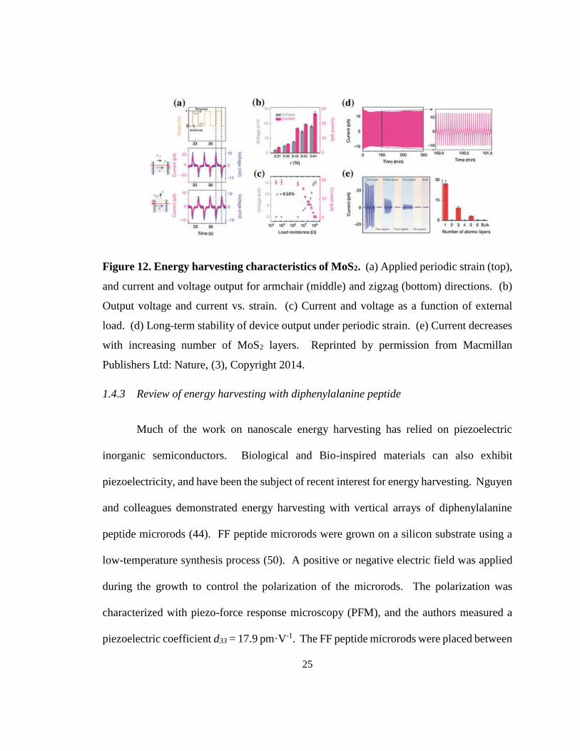
current and voltage were measured under a periodic strain. The device produced an open
circuit voltage of 18 mV at 0.64 % strain, and an output current of 27 pA as seen in figure
12a. Figure 12b shows the output voltage as a function of strain. Power generation is
shown in figure 12c, and was calculated by measuring the output across an external load
resistor under periodic 0.53 % strain. With an external load of 220 MΩ, the device
produced 2 mW·m-2, with an efficiency of 5 %. Figure 12d shows long term stability of
the device output.
The MoS2 generator was expanded to an array of multiple connected flakes. This
time, triangular MoS2 flakes were grown by CVD and transferred to a flexible PET
substrate. Differences in edge morphologies were observed to identify the “armchair”

24
direction on the flakes (63). As many as four MoS2 flakes were connected together. The
output current and voltage increased with the number of flakes. In addition to the number
of flakes, the piezoelectric potential was also investigated as a function of the number of
atomic layers in a single flake. No piezoelectricity was observed in flakes with an even
number of atomic layers, and piezoelectricity decreased with an increasing odd number of
layers as seen in figure 12e. This result is consistent with a theoretical study performed by
Zhou et al. (64). The results also suggest that MoS2 nanogenerators will have a
significantly lower capacitance than ZnO nanogenerators, making them well-suited for
high frequency energy harvesting.
Figure 11. Monolayer MoS2 nanogenerator. (a) Armchair and zigzag lattice directions
superimposed on MoS2 flake. (b) SHG data plotted in polar coordinates. (c) Completed
energy harvesting device with electrodes oriented to measure strain in the armchair
direction. (d) Schematic showing working mechanism of nanogenerator. Reprinted by
permission from Macmillan Publishers Ltd: Nature, (3), Copyright 2014.
25
Figure 12. Energy harvesting characteristics of MoS2. (a) Applied periodic strain (top),
and current and voltage output for armchair (middle) and zigzag (bottom) directions. (b)
Output voltage and current vs. strain. (c) Current and voltage as a function of external
load. (d) Long-term stability of device output under periodic strain. (e) Current decreases
with increasing number of MoS2 layers. Reprinted by permission from Macmillan
Publishers Ltd: Nature, (3), Copyright 2014.
1.4.3 Review of energy harvesting with diphenylalanine peptide
Much of the work on nanoscale energy harvesting has relied on piezoelectric
inorganic semiconductors. Biological and Bio-inspired materials can also exhibit
piezoelectricity, and have been the subject of recent interest for energy harvesting. Nguyen
and colleagues demonstrated energy harvesting with vertical arrays of diphenylalanine
peptide microrods (44). FF peptide microrods were grown on a silicon substrate using a
low-temperature synthesis process (50). A positive or negative electric field was applied
during the growth to control the polarization of the microrods. The polarization was
characterized with piezo-force response microscopy (PFM), and the authors measured a
piezoelectric coefficient d33 = 17.9 pm·V-1. The FF peptide microrods were placed between
26
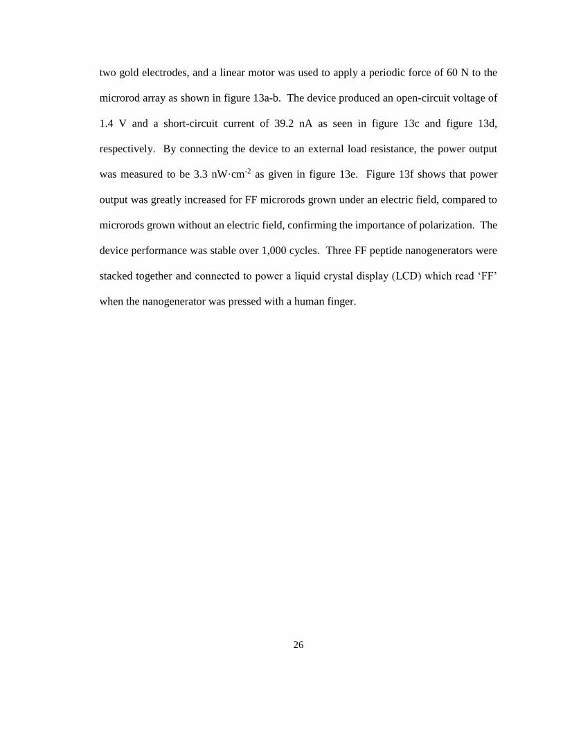
two gold electrodes, and a linear motor was used to apply a periodic force of 60 N to the
microrod array as shown in figure 13a-b. The device produced an open-circuit voltage of
1.4 V and a short-circuit current of 39.2 nA as seen in figure 13c and figure 13d,
respectively. By connecting the device to an external load resistance, the power output
was measured to be 3.3 nW·cm-2 as given in figure 13e. Figure 13f shows that power
output was greatly increased for FF microrods grown under an electric field, compared to
microrods grown without an electric field, confirming the importance of polarization. The
device performance was stable over 1,000 cycles. Three FF peptide nanogenerators were
stacked together and connected to power a liquid crystal display (LCD) which read ‘FF’
when the nanogenerator was pressed with a human finger.
27
Figure 13. Energy harvesting characteristics of FF peptide. (a) Schematic of device
structure. (b) Illustration of electrical measurement under applied force. (c) Open-circuit
voltage under periodic applied force. (d) Short-circuit current under periodic applied force.
(e) Power generation as a function of external load resistance for different polarization
conditions. (f) Output voltage as a function of force for different polarization conditions.
Reprinted from Nguyen, Vu, et al. "Self-assembly of diphenylalanine peptide with
controlled polarization for power generation." Nature communications 7 (2016):
13566.(44), (CC BY 4.0).
28
1.5 Review of strain and force sensing with piezotronic nanomaterials
1.5.1 Piezotronic strain sensing
Due to the fact that strains generate electric potentials in piezoelectric materials,
piezotronic devices are well-suited for strain and force sensing. It is the strain-generated
piezoelectric potentials that control charge transport across the metal-semiconductor
junction (56). Not surprisingly, the majority of piezotronic devices reported in the
literature are strain and force sensors. While there are many unique approaches to
piezotronic strain sensing, common themes emerge regarding materials, device
architecture, characterization, and performance.
1.5.2 Materials and morphology for piezotronic strain sensors
Most piezotronic strain sensors are based on materials such as ZnO and GaN. These
materials are most commonly synthesized as nanowires, although nanobelts and thin-film
approaches have also been explored (65-74). Nanowire devices may consist of either
single nanowires, or arrays of nanowires. The single nanowire approach allows for very
high sensitivity, while arrays of nanowires are robust and stable due to the redundancy of
multiple wires (65, 67, 70).
Flexible polymer substrates act as simple beams in bending. The outer surfaces of
the beam experience the highest bending stresses, either in tension or compression. Single
nanowires are commonly placed flat on the surface of such flexible substrates, and the
bending stress causes strain in the wire. Although nanowires placed on the surface of a
flexible substrate technically also experience bending stress, it is often reasonable to
assume that the nanowire is experiencing pure tension or compression due to the relative
29
size and material properties (65, 68, 74). The result is a piezopotential that develops along
the length of the nanowire between the source and drain electrodes. Vertically oriented
nanowire arrays can also measure strain due to the Poisson effect, and have achieved higher
gauge factors than single nanowire devices (67). Nanowires can be incorporated to form
hybrids with other materials such as carbon fibers, demonstrating the potential for fabric-
based piezotronic devices (72).
Although ZnO is most commonly used, piezotronic strain sensors have been
developed from other materials including ZnSnO3. Wu et al. achieved a gauge factor of
3740 for a ZnSnO3 nanowire strain sensor, the second highest value reviewed here (74).
ZnSnO3 is promising due to its high c-axis polarization, which was calculated to exceed
that of ZnO (74-76).
Single nanobelt strain sensors have been fabricated from GaN, which is reported to
have better atmospheric stability and acid resistance than ZnO (66). This work also
investigated the effect of c-axis orientation relative to bending direction. Liang et al.
demonstrated a strain sensor using a piezoelectric tellurium microwire (71).
1.5.3 Device architecture for piezotronic strain sensors
Common design elements exist among piezotronic, nanomaterial-based strain
sensors. The device is typically fabricated on a flexible substrate such as polyethylene
(PET) or polystyrene (PS). Piezotronic devices require a metal-semiconductor
heterojunction, with the metal forming either a Schottky or Ohmic contact with the
piezoelectric, semiconducting nanostructure, depending partly on the work function of the
metal (65-69, 71-74). High work function metals are typically used, especially gold, silver,
30
indium-tin-oxide (ITO), and platinum. The Schottky contact may be symmetric or
asymmetric, and the devices are usually encapsulated in PDMS or another polymer to
protect against contamination, corrosion, and physical damage.
Incorporating nanomaterials into strain sensing devices remains challenging. ZnO
nanowires are commonly grown using the low temperature hydrothermal method, or by
high temperature methods such as CVD (67, 69, 72). While hydrothermal synthesis is low
cost, scalable, and compatible with flexible polymer substrates, achieving long nanowires
remains difficult. Chemical vapor deposition readily results in long, high quality
nanowires, but the high temperatures are not compatible with polymer substrates or
photolithography patterning techniques (77). Thin-film piezotronics approaches are being
developed and show promise (78).
1.5.4 Device characterization and performance
Piezotronic devices are commonly characterized by their nonlinear, rectifying I-V
behavior, to which they owe their high sensitivity. The devices are driven by bias voltages
ranging from -3 V to + 3 V, and typical output currents are on the order of a few to tens of
microamps (65-69, 71-74). The metal-semiconductor-metal structure may have a Schottky
contact at each interface, or one of the contacts may be Ohmic (67). If the same metal is
used for both the source and drain electrode, the device will typically have a symmetric I-
V curve. Devices with different source and drain metals will have asymmetric barrier
heights at the metal-semiconductor junctions, resulting in rectifying behavior (67, 72).
Charge transport across the barrier can be explained by the thermionic emission diffusion
model (65, 74).
31
As a whole, piezotronic strain sensors exhibit several promising performance
characteristics. Piezotronic sensors are known for their high sensitivity and resolution, fast
response times, and stability. Yang et al. estimated that ZnO nanowires could achieve
response times as fast as 10 ms. ZnO nanowires were used to accurately detect AFM tip
vibrations from 0.11 to 0.33 Hz (68). Reported response times for piezotronic strain
sensors range from 10 ms to 500 ms (65, 69).
The figure of merit for strain sensors is called the gauge factor. Gauge factor is a
measure of sensitivity to strain, defined as the normalized change in current over the strain,
and given as
𝐺𝑎𝑢𝑔𝑒 𝐹𝑎𝑐𝑡𝑜𝑟 (𝐺𝐹) = |
∆𝐼𝐼0⁄
𝜀|
Where I0 is the zero strain current, and ΔI is the change in current due to a strain ε. The
highest reported gauge factor reviewed here for a piezotronic strain sensor was 4036 by
Zhang et al. (69). By comparison, a review of piezoresistive strain sensors based on
graphene reported gauge factors up to 300 (79). The gauge factor for a conventional metal
strain gauge is approximately 2 (80). Response times are typically measured by applying
periodic displacements with a linear motor or mechanical stage, and observing the dynamic
response of the output current. Measurements tend to be reproducible, with the I-V curve
returning to the unstrained state after unloading (65, 66). In principle, the piezotronic effect
is a persistent, but the current can drop in time due to charge trapping by impurities and
vacancies in the semiconductor (74). Therefore, the high quality, low defect nature of
many nanomaterials makes them appealing for piezotronics. The intrinsic
32
electromechanical coupling, high sensitivity and fast response times make piezotronic
devices ideal for strain sensing. A summary and comparison of reviewed piezotronic strain
sensors is provided in Table 1.
Zinc oxide nanowires are a common material for piezotronic strain sensors, due to
their semiconducting properties and enhanced piezoelectricity. Zhou et al. demonstrated a
characteristic example of a piezotronic ZnO nanowire strain sensor (65). Zinc oxide
nanowires were grown by thermal evaporation, with diameters between 2-6 µm and lengths
from hundreds of microns to millimeters. A single ZnO nanowire was transferred to a
flexible polystyrene substrate. Silver paste was used to connect each end of the nanowire
to the substrate as seen in figure 14a. The silver paste formed Schottky contacts with the
ZnO nanowire and served as the source and drain electrodes. PDMS was used to
encapsulate the device for protection.
33
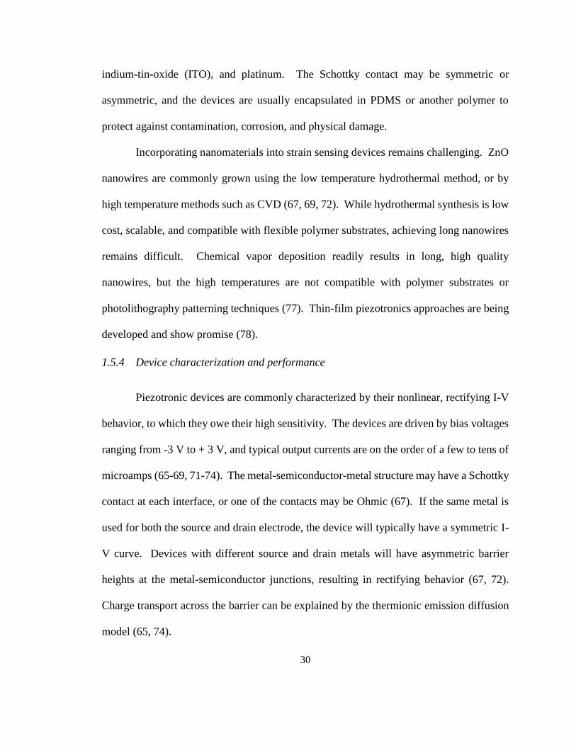
Figure 14. Single ZnO nanowire piezotronic strain sensor. (a) Strain measurement
setup. (b) I-V characteristic as a function of applied strain. (c) Gauge factor as a function
of strain. Adapted with permission from (65). Copyright 2008 American Chemical
Society.
The strain sensor was tested by fixing one end and attaching the other end to a
moveable stage as seen in figure 14b (65). The authors concluded that the nanowire
experienced pure tensile or compressive strains along the c-direction of the wire, based on
the geometry and mechanical properties of the device. Using a bias voltage of ± 1 V, the
authors measured the I-V behavior of the device for strains up to 0.98 %, shown in figure
14c. The results confirmed the existence of a rectifying, nonlinear Schottky contact
between the ZnO and silver paste. The sensitivity of the device was calculated for varying
strains and is presented in figure 14d. The device achieved a gauge factor of 1250, higher
than the value of 850 achieved by a piezoresistive carbon nanotube (CNT) sensor (81).

34
The device had a fast response time of 10 ms, and long-term performance was stable for
periodic deflections.
In addition to nanowires, nanobelts are another morphology commonly used for
strain sensors (69). Zhang et al. developed a ZnO nanobelt strain sensor with the source
and drain electrodes on the same monopolar ZnO surface. The use of the monopolar
surface greatly simplified device fabrication, and the nanobelt was doped with indium to
improve the mechanical properties. The 20 µm long by 180 nm wide nanobelt was placed
on a flexible polystyrene (PS) surface, and packaged with PDMS.
Device testing was accomplished by fixing one end of the sensor, and applying a
lateral displacement to the free end (69). I-V characteristics were measured for a bias
voltage swept over ± 3 V for strains from -0.4 % to + 0.3 %. The authors characterized the
change in Schottky barrier height as a function of bias voltage and applied strain. The
gauge factor was calculated for both tensile and compressive strains, with a maximum
gauge factor of 4036 for compressive strains and 135 for tensile strains. The authors
hypothesized that increased carrier mobility from the piezoresistive effect may have caused
screening, resulting in the large gauge factor difference. The response time of the device
was 120 ms.
35
Table 1. Comparison of strain sensing devices.
Material Morphology Gauge Factor Response Time Reference
ZnO NW, array 1813 (67)
ZnO NW, single 500 ms (68)
GaN NB, single (66)
ZnO/Carbon Fiber NW/fiber 81 (72)
ZnSnO3 NB, single (73)
ZnO (In doped) NB, single 4036 120 ms (69)
ZnO NW, single 1250 10 ms (65)
ZnSnO3 NW, single 3740 (74)
Te NW, single (71)
NW, nanowire; NB, nano/micro belts/ribbons.
1.5.5 Piezotronic pressure and force sensing
Piezotronic sensors can also be used to detect force and pressure, using the same
working principle as for strain sensing. The strain created by an applied force generates
piezopotentials which control charge carrier transport at the metal-semiconductor interface.
Device fabrication, materials, structure, and characterization are similar for force and strain
sensing, and force sensors can be fabricated on rigid or flexible substrates (82, 83). ZnO
nanowires are a common choice for force and pressure sensing as well. One key difference
between force and strain sensing lies in the application of force. In strain sensing, the
bending stress in a flexible substrate is experienced as an axial force along the c-axis of the
nanowire. In force sensing applications, axial forces are applied directly along the c-axis
of the nanowire (82, 84). Applications for piezotronic force sensors include handwriting
recognition, pressures switches, and e-skin (83, 85). Piezotronic force sensors are
especially interesting for e-skin applications, as they can achieve higher spatial density and
lower force sensing thresholds than mechanoreceptors in human skin (83, 86).
36
Wu et al. demonstrated a classic example of piezotronic pressure sensing with an
array of vertical ZnO nanowires (82). A flexible PET substrate was prepared with an ITO
bottom electrode pattern made of Cr/Au/ITO. A ZnO seed layer was deposited and
patterned on the electrodes, and arrays of vertical ZnO nanowires were grown on the seed
layer. The ZnO nanowires were 30 µm long and patterned into 20 µm x 20 µm taxels. The
nanowires were packaged in SU8, and a gold top electrode was deposited to complete the
device. A Schottky contact formed between the nanowires and gold, creating an
addressable array of Strain Gated Vertical Piezotronic Transistors (SGVPT). The nanowire
taxels had a spatial density of 8464 taxels·cm-2, compared to a spatial density of 240 cm-2
for mechanoreceptors in a human hand (86). The current output from a single taxel was
measured for increasing pressure. The saturation pressure was 30 kPa, and the pressure
sensing range of the device was comparable to that of a human finger (87). The sensitivity
of the pressure sensor is indicated by the change in carrier transport due to the
piezopotential, and was calculated to be 2.1 µS·kPa-1. The response time of the device was
measured to be 0.15 seconds. The sensor proved to be useful for handwriting detection,
and the imprint of the letter “A” could be resolved by reading the outputs from different
channels across the sensor. The device showed a stable output response over 1,000 bending
cycles.
The piezotronic effect can also control charge carrier transport in optoelectronic
devices, by what is known as the piezo-phototronic effect. Although commonly associated
with light emitting diodes (LEDs) and photodetectors, the piezo-phototronic effect has
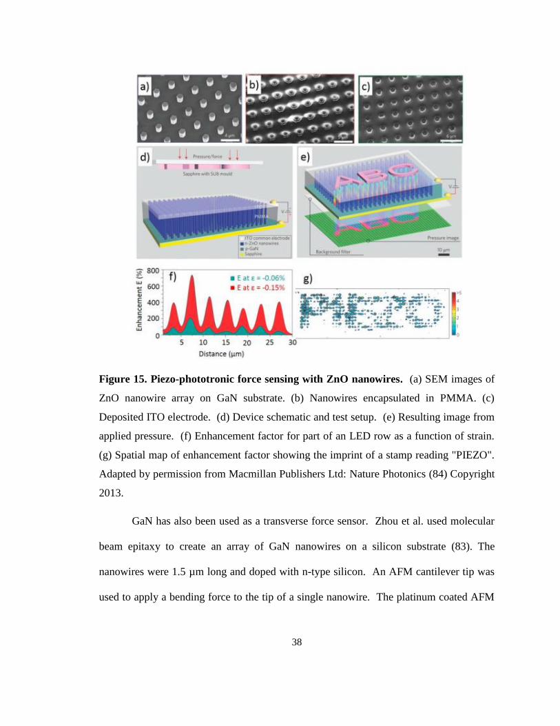
found applications in pressure sensing. Pan et al. created an array of pressure sensing LEDs
37
by combining ZnO nanowires with GaN (84). An array of single ZnO nanowires with
diameters of 1.5 µm and a 4 µm spacing was grown on p-type GaN as seen in figure 15a.
A Ni/Au electrode layer was deposited on the back side of the GaN, and the nanowires
were packaged with PMMA as shown in figure 15b. ITO was deposited on the exposed
nanowires as the top electrode, shown in figure 15c. The device and working mechanism
are illustrated in figure 15d and figure 15e, respectively. To test the pressure response of
the LED array, the authors created a text stamp out of SU8 that spelled “piezo”. The stamp
was pressed onto the device with strains varying from -0.06 to -0.015, and the output
intensity of the LEDs was measured with a CCD sensor and spectrometer. The measured
LED intensity was scaled against the unstressed intensity to calculate a so called
enhancement factor, as seen in figure 15f. The average enhancement factor was 2, and the
response time of the sensor was 90 ms. A spatial map of the enhancement factors
corresponding to the imprint of the “piezo” stamp is shown in figure 15g.
38
Figure 15. Piezo-phototronic force sensing with ZnO nanowires. (a) SEM images of
ZnO nanowire array on GaN substrate. (b) Nanowires encapsulated in PMMA. (c)
Deposited ITO electrode. (d) Device schematic and test setup. (e) Resulting image from
applied pressure. (f) Enhancement factor for part of an LED row as a function of strain.
(g) Spatial map of enhancement factor showing the imprint of a stamp reading "PIEZO".
Adapted by permission from Macmillan Publishers Ltd: Nature Photonics (84) Copyright
2013.
GaN has also been used as a transverse force sensor. Zhou et al. used molecular
beam epitaxy to create an array of GaN nanowires on a silicon substrate (83). The
nanowires were 1.5 µm long and doped with n-type silicon. An AFM cantilever tip was
used to apply a bending force to the tip of a single nanowire. The platinum coated AFM
39
tip formed a Schottky contact with the GaN nanowire, and silver paste was used as the
bottom electrode, creating a second Schottky contact.
The band diagram showed how the barrier height changes due to the piezopotential
(83). Forces ranging from 104 nN to 312 nN were applied to the nanowire, and the I-V
response was measured. The asymmetric I-V response was due to the differences in work
functions for silver and platinum, and the response was dominated by the Pt/GaN Schottky
contact. The sensitivity of the devices depends on the applied force due to the nonlinear I-
V curve. The sensitivity was calculated to be 0.5 pA/nN and 2.0 pA/nN for forces ranging
from 16-32 nN and 64-80 nN, respectively. The sensitivity was linearized by ln(I) for
simplification. The response time was measured to be less than 5 ms.
Zhou et al. developed a piezotronic trigger sensor which could detect impact forces
(85). A single ZnO microwire, approximately 1 mm long, was connected to a Si/SiO2
substrate with silver paste. The free end of the wire formed a Schottky contact with a gold-
coated tungsten needle. Argon gas was blown against the microwire, causing it to vibrate
against the needle, simulating an impact force. Impacts were detected by measuring the
voltage generated in the nanowire. In a laterally bent microwire, the potential distribution
occurs across the diameter of the wire, instead of along the length. Voltage measurements
were taken on both the tension and compression sides of the wire. To measure the I-V
response, a constant mechanical force was applied to the wire and the current was measured
for a bias ranging over ± 2 V.
Piezotronic force sensors have achieved force sensing thresholds as low as 4 nN
with a resolution of 0.5 pA/nN (83). Spatial resolutions of 2.7 µm have been demonstrated,
40
and fatigue resistant, single crystal nanomaterials provided stable sensing for over 1,000
cycles (82, 84). Table 2 provides a summary and comparison of piezotronic force and
pressure sensors.
Table 2. Comparison of force and pressure sensing devices.
Material Morphology Sensitivity Spatial
Resolution
Response
Time
Reference
GaN NW, single 0.5 – 2 pA/nN < 5 ms (83)
ZnO NW, array 2.1 µS·kPa-1 100 µm 150 ms (82)
ZnO NW, single 10 ms (85)
ZnO NW, array 12.88 GPa-1 2.7 µm 90 ms (84)
NW, nanowire.
1.6 Scope of this Thesis
In essence, piezoelectricity is the transformation of mechanical energy into
electrical energy, and vice versa. Piezoelectric materials are the medium for this energy
transformation, which can be controlled through the use of various nanomaterials and
nanostructures. This thesis seeks to address barriers to the development of new
piezoelectric nanomaterial devices for sensing and energy harvesting. Finite element
models are developed to gain insight into the behavior of an emerging piezoelectric
nanomaterial, and current fabrication techniques are expanded to new substrate materials
to realize new device designs. Chapter 1 provides background on the theory of
piezoelectricity, and a review of common piezoelectric nanomaterials. Next, the
piezotronic effect is introduced, a sensing principle enabled by piezoelectric nanomaterials
with semiconducting properties. Chapter 1 concludes with a review of energy harvesting
with piezoelectric nanomaterials, followed by a review of piezotronic force and strain
sensors.
41
The contributions of this thesis begin with chapter 2, which explores the
piezoelectric behavior of diphenylalanine (FF) peptide, a bio-inspired piezoelectric
material, through finite element modeling. A flexible FF peptide nanogenerator is
fabricated, demonstrating energy harvesting and validating the predictions of the finite
element models. Chapter 3 details the modeling and fabrication of piezotronic force and
strain sensors, with a focus on applications for haptics and prosthetic limbs. Using
mechanical transfer, CVD synthesis of ZnO nanowires is expanded to soft polymer
substrates to create a stretchable piezotronic strain sensor. Chapter 4 is motivated by
challenges associated with chemical vapor deposition (CVD), a common technique for
piezoelectric nanomaterial synthesis. The design and verification of a new apparatus for
CVD synthesis is presented, which can allow for the use of low-temperature substrates in
a high-temperature CVD furnace. Finally, chapter 5 provides conclusions and outlook on
the future of piezoelectric nanomaterials for sensing and energy harvesting applications.
42
Chapter 2. Modeling and fabrication of a flexible piezoelectric
nanogenerator with diphenylalanine peptide
Mechanical energy can be found in the environment in many forms including wind,
water, mechanical vibration, and human movement. By harvesting this energy with
nanogenerators, self-powered systems can be realized such as sensors for structural
monitoring, environmental measurement, and chemical and biosensing (62, 73, 88-93).
Due to their inherent electromechanical coupling, piezoelectric nanomaterials are well-
suited for harvesting mechanical energy. Piezoelectric nanogenerators have been
successfully developed based on materials such as zinc oxide (ZnO), Poly(vinylidene
fluoride-trifluoroethylene) (P(VDF-TrFE)) and monolayer molybdenum disulfide (MoS2)
(3, 16, 59, 60, 94-99).
Due to its biological origins, strong piezoelectricity, and demonstrated ability to
self-assemble, diphenylalanine (FF) peptide has received much recent interest.
Diphenylalanine peptide is being explored for potential applications for drug delivery, and
is also significant for its role as the core recognition motif for Alzheimer’s beta amyloid
(5, 43). Diphenylalanine-based dipeptides can self-assemble into nanotubes, microrods,
hydrogels, and other structures (39-42). Self-assembled FF peptide nanotubes have a
hexagonal structure with promising mechanical and piezoelectric properties. Reported
elastic modulus values range from 19-27 GPa, which is relatively high among biomaterials
(46, 47). The origins of this high stiffness have been explored through first principles (48).
Poling can improve the piezoelectric properties of FF peptide, with reported values for the
piezoelectric coefficient d33 up to 18 pm/V (49, 50). The first use of FF peptide with
43
controlled polarization for power generation was recently demonstrated on a rigid substrate
(44). Due to its promising electromechanical properties, biocompatibility, and low-
temperature synthesis method, there is growing interest in FF peptide as a piezoelectric
nanomaterial for applications such as energy harvesting.
Despite the potential of FF peptide as a piezoelectric, bio-inspired material, there
are still significant barriers to its adoption for device applications. The first barrier is the
need for comprehensive finite element models of piezoelectricity in FF peptide structures.
First principles and finite element models have provided insight into the mechanical
properties of FF peptide microstructures and bulk material (46, 48). However, more work
is needed to study the piezoelectric performance of FF peptide compared to conventional
piezoelectric materials. Additionally, there is a need to study the complex interactions and
piezoelectric response of FF peptide structures as part of a completed device. Design,
fabrication, and testing of new devices is complex, costly, and time consuming. Without
finite element models, it is difficult to fully predict the piezoelectric response of FF peptide
devices, posing a challenge for device design. Finite element modeling has been used to
predict the behavior of piezoelectric nanogenerators based on ZnO material (100-102). The
development of finite element models for FF peptide nanogenerators can provide insight
into the design and optimization of FF peptide devices.
The second barrier to wider use of FF peptide is the need to realize its promising
piezoelectric properties in a flexible device. Transitioning from rigid to flexible substrates
presents challenges for material synthesis, device fabrication, and characterization. These
challenges were overcome to develop a flexible FF peptide nanogenerator. The device was
44
characterized, and power generation from bending deformation was demonstrated.
Characterization of the fabricated nanogenerator successfully validated the predictions of
the finite element model. The realization of a flexible FF peptide nanogenerator can help
to expand the use of FF peptide to new applications that are inaccessible to rigid substrates,
such as wearable devices, flexible electronics, and soft robotics.
2.1 Finite element model of a single nanowire
A 3D model of a single nanowire was created using COMSOL Multiphysics to
compare the piezoelectric behavior of FF peptide to conventional piezoelectric materials.
The nanowire model was validated against results and geometry from a previous study of
piezoelectricity in a ZnO nanowire (16, 103). After validation, the nanowire model
dimensions were set to a diameter of 50 nm, and a length of 500 nm. Dimensions were
constant for all materials. Electrical and mechanical properties for FF peptide were sourced
from computational and experimental literature, and are provided in Table 3. The electrical
and mechanical properties for all other materials were taken from the COMSOL
Multiphysics standard materials library (104).
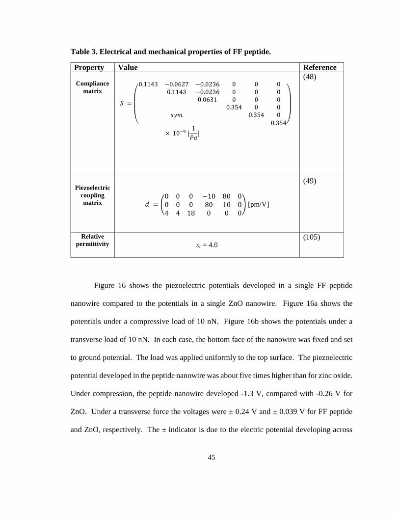
45
Table 3. Electrical and mechanical properties of FF peptide.
Property Value Reference
Compliance
matrix
𝑆 =
(
0.1143 −0.0627 −0.0236 0 0 0 0.1143 −0.0236 0 0 0 0.0631 0 0 0 0.354 0 0 𝑠𝑦𝑚 0.354 0 0.354)
× 10−9 [1
𝑃𝑎]
(48)
Piezoelectric
coupling
matrix
𝑑 = (0 0 0 −10 80 00 0 0 80 10 04 4 18 0 0 0
) [pm/V]
(49)
Relative
permittivity
εr = 4.0
(105)
Figure 16 shows the piezoelectric potentials developed in a single FF peptide
nanowire compared to the potentials in a single ZnO nanowire. Figure 16a shows the
potentials under a compressive load of 10 nN. Figure 16b shows the potentials under a
transverse load of 10 nN. In each case, the bottom face of the nanowire was fixed and set
to ground potential. The load was applied uniformly to the top surface. The piezoelectric
potential developed in the peptide nanowire was about five times higher than for zinc oxide.
Under compression, the peptide nanowire developed -1.3 V, compared with -0.26 V for
ZnO. Under a transverse force the voltages were ± 0.24 V and ± 0.039 V for FF peptide
and ZnO, respectively. The ± indicator is due to the electric potential developing across
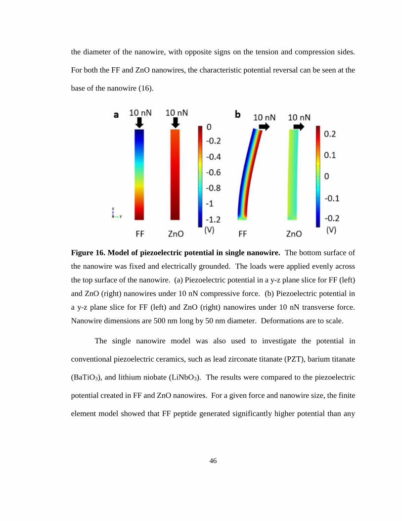
46
the diameter of the nanowire, with opposite signs on the tension and compression sides.
For both the FF and ZnO nanowires, the characteristic potential reversal can be seen at the
base of the nanowire (16).
Figure 16. Model of piezoelectric potential in single nanowire. The bottom surface of
the nanowire was fixed and electrically grounded. The loads were applied evenly across
the top surface of the nanowire. (a) Piezoelectric potential in a y-z plane slice for FF (left)
and ZnO (right) nanowires under 10 nN compressive force. (b) Piezoelectric potential in
a y-z plane slice for FF (left) and ZnO (right) nanowires under 10 nN transverse force.
Nanowire dimensions are 500 nm long by 50 nm diameter. Deformations are to scale.
The single nanowire model was also used to investigate the potential in
conventional piezoelectric ceramics, such as lead zirconate titanate (PZT), barium titanate
(BaTiO3), and lithium niobate (LiNbO3). The results were compared to the piezoelectric
potential created in FF and ZnO nanowires. For a given force and nanowire size, the finite
element model showed that FF peptide generated significantly higher potential than any
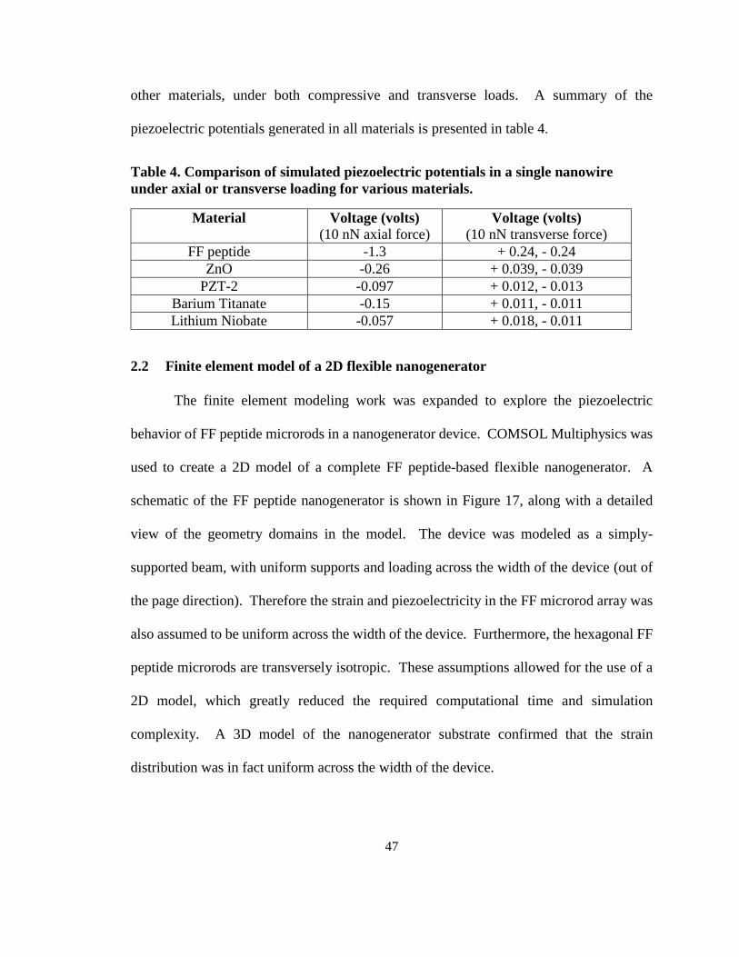
47
other materials, under both compressive and transverse loads. A summary of the
piezoelectric potentials generated in all materials is presented in table 4.
Table 4. Comparison of simulated piezoelectric potentials in a single nanowire
under axial or transverse loading for various materials.
Material Voltage (volts)
(10 nN axial force) Voltage (volts)
(10 nN transverse force)
FF peptide -1.3 + 0.24, - 0.24
ZnO -0.26 + 0.039, - 0.039
PZT-2 -0.097 + 0.012, - 0.013
Barium Titanate -0.15 + 0.011, - 0.011
Lithium Niobate -0.057 + 0.018, - 0.011
2.2 Finite element model of a 2D flexible nanogenerator
The finite element modeling work was expanded to explore the piezoelectric
behavior of FF peptide microrods in a nanogenerator device. COMSOL Multiphysics was
used to create a 2D model of a complete FF peptide-based flexible nanogenerator. A
schematic of the FF peptide nanogenerator is shown in Figure 17, along with a detailed
view of the geometry domains in the model. The device was modeled as a simply-
supported beam, with uniform supports and loading across the width of the device (out of
the page direction). Therefore the strain and piezoelectricity in the FF microrod array was
also assumed to be uniform across the width of the device. Furthermore, the hexagonal FF
peptide microrods are transversely isotropic. These assumptions allowed for the use of a
2D model, which greatly reduced the required computational time and simulation
complexity. A 3D model of the nanogenerator substrate confirmed that the strain
distribution was in fact uniform across the width of the device.

48
The model geometry was constructed from a series of rectangular domains. The PI
peptide growth substrate was represented by a 12 mm long and 0.25 mm tall rectangle.
Based on measurements of the SEM image in figure 20b, the peptide microrods were
modeled as 50 µm long by 7 µm wide rectangles. The microrods were placed directly on
top of the PI growth substrate in a row with a spacing of 40 µm. A rectangle layer with a
size of 12 mm long by 75 µm tall was placed on top of the growth substrate, overlapping
the microrods. This rectangle represented the PDMS layer in which the microrods were
embedded. The gold electrode layers were omitted from the simulation due to their
negligible thickness (100 nm). The nanogenerator model was placed on top of a 30 mm
long by 0.25 mm tall PET rectangle. The PET surface represented an example of a typical
flexible application. Mechanical properties for PDMS, PET, and PI were taken from the
COMSOL material library. For this simulation, PDMS, PET, and PI were modeled as
linear elastic materials, and linear elasticity was assumed for the model physics. The d33
direction for the piezoelectric material was aligned with the +y direction in the simulation.
A distributed load was applied to a portion of the top surface of the nanogenerator, resulting
in a 3.5 mm displacement at the center.
The nanogenerator model and corresponding geometry domains are shown in figure
17a. The mechanical and electrical boundary conditions used for the model are shown in
figure 17b. The nanogenerator on a flexible PET surface was modeled as a simply-
supported beam, with a pin at x = 6 mm, and a roller at x = 24 mm. The pin was modeled
as a fixed displacement in both the x and y directions, while the roller was modeled as a
fixed displacement in the y direction only. A uniform distributed load of 32 kPa was
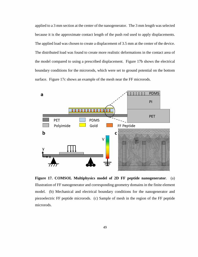
49
applied to a 3 mm section at the center of the nanogenerator. The 3 mm length was selected
because it is the approximate contact length of the push rod used to apply displacements.
The applied load was chosen to create a displacement of 3.5 mm at the center of the device.
The distributed load was found to create more realistic deformations in the contact area of
the model compared to using a prescribed displacement. Figure 17b shows the electrical
boundary conditions for the microrods, which were set to ground potential on the bottom
surface. Figure 17c shows an example of the mesh near the FF microrods.
Figure 17. COMSOL Multiphysics model of 2D FF peptide nanogenerator. (a)
Illustration of FF nanogenerator and corresponding geometry domains in the finite element
model. (b) Mechanical and electrical boundary conditions for the nanogenerator and
piezoelectric FF peptide microrods. (c) Sample of mesh in the region of the FF peptide
microrods.
50
Figure 18a shows the initial state of the nanogenerator, and the bending stresses in
the deformed state. Discontinuities in the stress distribution can be seen due to the different
elastic moduli in the PET, PI, and PDMS layers as shown in figure 18b. The maximum
and minimum stresses in the beam were 27.3 MPa and -92.2 MPa, respectively. The strain,
shown in figure 18c, was continuous between the layers, as expected. With the exception
of localized stress concentrators, the strains were generally within ~2 %, confirming that
the device could be modeled using linear elasticity.
Figure 18. Stress and strain in 2D model of FF peptide nanogenerator. A 32 kPa
distributed load was applied in the middle of the nanogenerator, producing a maximum
deflection of 3.5 mm. (a) Stress tensor xx component in the nanogenerator showing the
initial and deformed state. (b) Detailed view of the xx component of the stress tensor across
the material boundaries. (c) Detailed view of the strain tensor xx component across the
material boundaries.
51
Figure 19 shows the piezoelectric potential in the FF microrods under a 3.5 mm
deflection, as a function of their position on the nanogenerator. The bottom surfaces of the
microrods were grounded. The electric potential was measured at the top of each microrod
and plotted in figure 19a. The electric potential in the microrod is shown on the vertical
axis, and the horizontal axis is the location of the microrod on the nanogenerator. The
electric potential was measured at a point in the center of the top surface of each microrod.
In reality, the potential across the top surface of each microrod was slightly non-uniform
in the simulation, due to the complex strain state. For an individual microrod, the variation
in potential across the top surface was approximately 0.1 V or less.
Figure 19a shows that the microrods in the nanogenerator can be divided into three
regions based on electric potential. Region II is in the middle of the nanogenerator, under
the distributed load. Region I and III are towards the outside edges of the nanogenerator
where no distributed load was applied. Due to device symmetry, Region I and Region III
have similar electric potentials. In Region I and Region III, the piezoelectric potential in
the microrods decreases slowly towards the center of the nanogenerator, from about -0.2
V to about -0.3 V. At the boundaries with Region II, the piezoelectric potential rapidly
drops to -1.6 V. Figure 19b shows the piezoelectric potential distribution in a group of
microrods in Region I, at x = 11 mm. Figure 19c shows the potential in a group of
microrods in Region II, at x = 15 mm. Overall, the displacement of the nanogenerator
creates an electric potential distribution along the length of the microrods in figure 19b and
figure 19c. However, a complex potential distribution exists near the root of the microrods.
The complex strain and potential near the root area is likely caused by the interface between
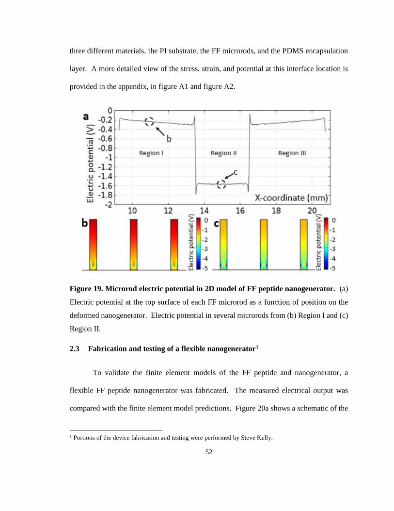
52
three different materials, the PI substrate, the FF microrods, and the PDMS encapsulation
layer. A more detailed view of the stress, strain, and potential at this interface location is
provided in the appendix, in figure A1 and figure A2.
Figure 19. Microrod electric potential in 2D model of FF peptide nanogenerator. (a)
Electric potential at the top surface of each FF microrod as a function of position on the
deformed nanogenerator. Electric potential in several microrods from (b) Region I and (c)
Region II.
2.3 Fabrication and testing of a flexible nanogenerator1
To validate the finite element models of the FF peptide and nanogenerator, a
flexible FF peptide nanogenerator was fabricated. The measured electrical output was
compared with the finite element model predictions. Figure 20a shows a schematic of the
1 Portions of the device fabrication and testing were performed by Steve Kelly.
53
fabricated nanogenerator. The fabricated device has the same structure and dimensions as
the finite element model in figure 17. Arrays of vertical FF peptide microrods with
controlled polarization were grown on flexible, gold-coated PI substrates using a low
temperature synthesis method (44, 50). Polyimide film squares (DuPont Kapton) were
laser cut with dimensions of 12 mm long x 12 mm wide x 0.25 mm thick to serve as flexible
growth substrates for the FF peptide microrods. Sputtering was used to deposit a 5 nm
thick chromium (Cr) adhesion layer followed by a 100 nm thick gold (Au) electrode layer.
The synthesis method for the growth of FF peptide microrods is discussed in detail in (50),
and the growth of vertical FF microrod arrays on the flexible PI substrates is briefly
summarized here. A solution of FF peptide powder (Bachem) was dissolved in
Hexafluoroisopropanol (HFP) and dropped onto the PI substrates in a vacuum chamber.
The chamber was then evacuated and purged with dry air, which resulted in the formation
of amorphous FF peptide seed layers. Next, the substrates were placed between two
parallel aluminum plates in a chamber with controlled humidity. The substrates were
subjected to a uniform electric field by applying 5 kV to the parallel plates. Meanwhile,
100 % relative humidity (RH) air was circulated across the substrates for 60 seconds. This
process crystallized the amorphous seed layers. During this process, the PI substrates were
affixed between the two parallel aluminum plates with a non-conductive tape. Previously,
a conductive carbon tape was used to mount rigid silicon substrates between the poling
plates (44, 50). Replacing the conductive tape with the non-conductive tape resulted in a
more uniform seed layer on the insulating PI substrates. Further investigation is needed to
determine the reason for this improvement. Finally, the substrates with crystallized seed

54
layers were floated face-down in a 5 ml solution of FF peptide dissolved in water. The
substrates were left in the solution for 6 hours at 55 °C. During this time, the substrates
were again poled under a uniform electric field between two parallel aluminum plates with
a voltage of 8.5 kV.
The substrates with FF peptide microrod arrays were spin-coated with PDMS
(Slygaard 184) at 4,000 RPM for 2 minutes, and cured. Next, a top electrode layer was
sputtered on the PDMS consisting of a 5 nm thick Cr adhesion layer and a 100 nm thick
Au layer. The completed FF peptide nanogenerator was attached to a 30 mm long x 12
mm wide x 0.25 mm thick layer of PET for testing.
SEM imaging of the peptide growth showed an array of peptide microstructures
that can be seen in the inset of figure 20b. The microrods in the SEM image were
approximately 50 µm long by 7 µm in diameter. Figure 20b shows a picture of the
completed FF nanogenerator device. The nanogenerator was attached to a long, thin piece
of PET which represents a flexible surface that the nanogenerator could be attached to.
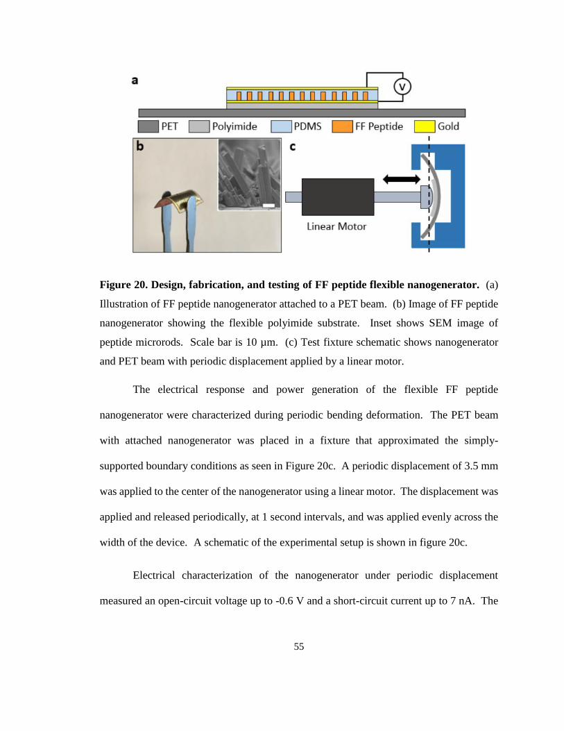
55
Figure 20. Design, fabrication, and testing of FF peptide flexible nanogenerator. (a)
Illustration of FF peptide nanogenerator attached to a PET beam. (b) Image of FF peptide
nanogenerator showing the flexible polyimide substrate. Inset shows SEM image of
peptide microrods. Scale bar is 10 µm. (c) Test fixture schematic shows nanogenerator
and PET beam with periodic displacement applied by a linear motor.
The electrical response and power generation of the flexible FF peptide
nanogenerator were characterized during periodic bending deformation. The PET beam
with attached nanogenerator was placed in a fixture that approximated the simply-
supported boundary conditions as seen in Figure 20c. A periodic displacement of 3.5 mm
was applied to the center of the nanogenerator using a linear motor. The displacement was
applied and released periodically, at 1 second intervals, and was applied evenly across the
width of the device. A schematic of the experimental setup is shown in figure 20c.
Electrical characterization of the nanogenerator under periodic displacement
measured an open-circuit voltage up to -0.6 V and a short-circuit current up to 7 nA. The
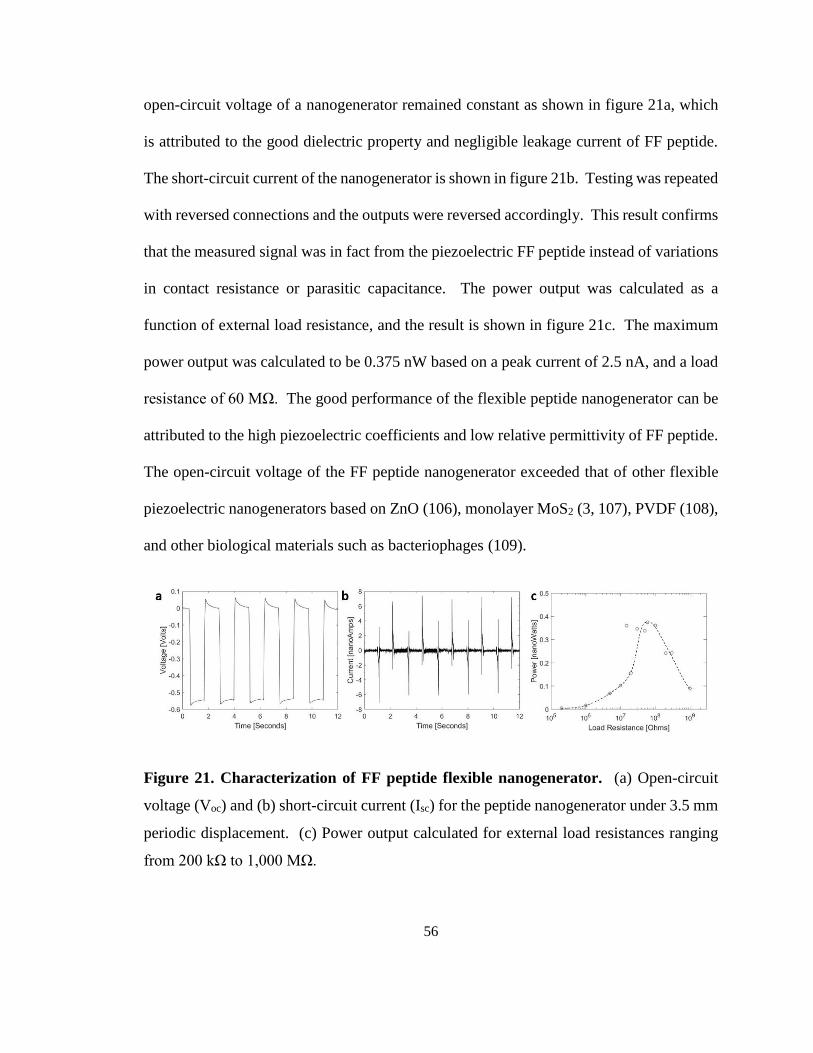
56
open-circuit voltage of a nanogenerator remained constant as shown in figure 21a, which
is attributed to the good dielectric property and negligible leakage current of FF peptide.
The short-circuit current of the nanogenerator is shown in figure 21b. Testing was repeated
with reversed connections and the outputs were reversed accordingly. This result confirms
that the measured signal was in fact from the piezoelectric FF peptide instead of variations
in contact resistance or parasitic capacitance. The power output was calculated as a
function of external load resistance, and the result is shown in figure 21c. The maximum
power output was calculated to be 0.375 nW based on a peak current of 2.5 nA, and a load
resistance of 60 MΩ. The good performance of the flexible peptide nanogenerator can be
attributed to the high piezoelectric coefficients and low relative permittivity of FF peptide.
The open-circuit voltage of the FF peptide nanogenerator exceeded that of other flexible
piezoelectric nanogenerators based on ZnO (106), monolayer MoS2 (3, 107), PVDF (108),
and other biological materials such as bacteriophages (109).
Figure 21. Characterization of FF peptide flexible nanogenerator. (a) Open-circuit
voltage (Voc) and (b) short-circuit current (Isc) for the peptide nanogenerator under 3.5 mm
periodic displacement. (c) Power output calculated for external load resistances ranging
from 200 kΩ to 1,000 MΩ.
57
The flexible nanogenerator consisting of FF microrods and the adjacent polymer
matrix can be modeled as a capacitor-type device. The capacitance of the device is the
sum of the capacitance for the microrods and the capacitance for the PDMS matrix. The
total charges, on the other hand, are contributed solely by the piezoelectric microrods.
Based on SEM images, the volume fraction of vertical FF microrods can be estimated to
be 25-33 %. For calculation purposes, the volume fraction was assumed to be 30 %. The
main contribution was assumed to be from the microrods in Region II, and the piezoelectric
potential of the microrods was taken to be -1.6 V from the finite element analysis. Based
on these values, it was estimated that the nanogenerator would produce a Voc of
approximately -0.61 V, which was consistent with the experimental measurement of -0.6
V. The close agreement between the simulation and measured device output confirms the
validity of the model. This result demonstrates the importance and significance of
developing finite element models for the design and optimization of FF peptide devices.
2.4 Chapter summary
Finite element models were used to study the piezoelectric potential in FF peptide.
For a given force, the piezoelectric potential in a single nanowire model was found to be
higher for FF peptide than for conventional piezoelectric materials such as ZnO, PZT,
BaTiO3, and LiNbO3. The finite element analysis was expanded to create a 2D model of a
flexible nanogenerator based on FF peptide microrods. To validate the model predictions,
the first flexible FF peptide nanogenerator with vertical microrods was fabricated. The
nanogenerator was tested, and successfully harvested mechanical energy from bending
deformation. The electrical output of the fabricated device was characterized and the

58
results successfully validated the finite element model of the nanogenerator. The
expansion of FF peptide growth to flexible substrates opens the way for new applications
including wearable devices and flexible electronics. Finite element models can provide
insight into the design and optimization of a new generation of flexible FF peptide devices.

59
Chapter 3. Modeling and fabrication of piezotronic force and strain
sensors
3.1 Tactile sensing for haptics and prosthetic limbs
There were 1.6 million amputees in the United States alone as of 2005, with the
number projected to double by 2050 (110). There are many types of upper limb prostheses
available. The choices of whether or not to use a prosthesis, and what type of device to
use, are highly individual decisions, and there is no correct answer. For some individuals,
however, the incorporation of sensory feedback into prosthetic limbs can be beneficial. It
has been estimated that 20 % of eligible users decide not to use a prosthetic device, and
lack of sensory feedback is cited as a major reason. Recent trials have demonstrated
increased prosthesis utility with the incorporation of sensory feedback. However,
incorporation of sensory input exists in only a relatively small number of trials, which often
rely on invasive peripheral nervous system interfaces (111, 112). There has been
significant work to develop sensors for so called electronic skin (e-skin) that can replicate
human touch perception (113).
The goal of this work is to purpose-design a tactile sensor for haptics and
prosthetics applications. The sensor will be intended for use with a sensory substitution
system for upper limb prostheses. While sensory substitution systems already exists, they
often rely on off-the-shelf sensors which are not optimized for this application (114, 115).
Current state of the art upper limb prostheses allow users to exhibit voluntary motor
control of the device, but there are limited options for providing sensory feedback. Several
works show that implementation of sensory feedback greatly improves closed-loop control

60
of prosthetic devices, which currently is limited to visual feedback (111, 112). At present,
several research trials have demonstrated success in connecting off-the-shelf sensors to the
peripheral nerves in the arm (112). These trials rely on invasive surgical interface
technologies such as cuff electrodes and are limited to pressure or force sensing (112).
Results of these trials have been promising, showing increased prosthesis functionality and
addressing problems such as phantom limb pain. Furthermore, these trials have been
conducted for extended periods of up to 24 months (111).
Current state of the art sensors can exceed the spatial density of the human
mechanoreceptor system and provide sensing within physiological force ranges. However,
the large amounts of data generated by such sensors are difficult to incorporate into the
peripheral nervous system (84, 112). Machine learning classifiers have found use in
robotics to transform complex inputs from high-resolution sensors into discrete outputs
(116). These concepts are applicable to the development of vibrotactile (VT) interfaces,
which belong to a growing body of noninvasive haptic stimulation literature including
mechanotactile and surface electrical stimulation (114, 117).
While current developments are very promising and show a strong interest in this
field, there are many opportunities to develop purpose-designed sensors. Just as the choice
of prosthesis type varies by user needs, the preferred type of sensory input may also be user
dependent. Piezotronic force and strain sensors are well-suited for replicating human
tactile perception, due to their high sensitivity and high spatial resolution.
The ability to reliably grasp objects is an important feature for many upper limb
prosthesis designs. Controlling the grasp force on an object is important not only to avoid

61
damaging the object, but also for preventing object slip. Grasp force control in prosthetic
hands is a complex problem involving sensor design, feedback control, and machine
learning (118). Although shear force sensors can detect object slip, most work has been
focused on the development of controllers and algorithms for slip detection. A wide variety
of slip detection approaches and sensor architectures have been studied, but no clear metric
exists for sensor performance in grasping applications. There is a need to continue
developing sensors and methods to improve grasping with prosthetic hands for preventing
object slip.
This chapter begins with the design of a piezotronic sensor architecture that can
detect physiological force ranges for both normal and shear contact forces. The
requirements for the tactile sensor are informed by the tactile sensing capabilities of human
touch physiology. These aspects include force, form, texture, and curvature (shape) (119).
The human somatosensory system contains 4 distinct neuronal structures called
mechanoreceptors. The mechanoreceptors are classified based on their response as rapidly
adapting (RA) or slowly adapting (SA). RA receptors respond transiently to forces on the
skin while SA receptors respond for the entire duration of the applied force. The RA
receptor types are the Meissner (RA type I) and Pacinian corpuscles (RA type II). The SA
receptor types are the Merkel disks (SA type I) and Ruffini endings (SA type II) (120).
The Pacinian corpuscles are sensitive to vibration and pressure while the Meissner
corpuscles sense light touch. The Merkel disks also detect vibration and pressure, and the
Ruffini endings are sensitive to skin stretch. Additionally, each type of structure has a
differently sized receptive field and varying spatial density, which is generally highest in
62
the hand (121). Using single unit recordings and the von Frey hair test method, the median
force sensing thresholds for human mechanoreceptors were found to be 0.58 mN and 0.54
mN for RA I and RA II types and 1.3 mN and 7.5 mN for SA I and SA II types, respectively
(122). For texture sensitivity, it has been reported that the human hand can detect textures
at the nanoscale (123).
The literature presents two general approaches to tactile sensor design. The first
group consists of conventional MEMS, and includes piezoresistive, capacitive, and
optoelectric sensors. The second group involves hybrid biological devices (124). Within
the two groups, the biggest differentiators are fabrication cost, resolution, and number of
sensing modes (e.g. shear and normal force).
The majority of devices reviewed here are conventional, and within this group most
are capacitive. A micro-machined capacitive device with floating electrodes is presented
by Cheng, et al. The device is simple and economical with resolution as low as 38 mN
(125). Using microfluidics and capacitive sensing, a flexible, normal force sensor with 5
mm spatial resolution is demonstrated (126). Other capacitive sensor designs exhibit
multimodal sensing to detect shear and normal forces, however the range is limited to 10
mN (127). Sub-mN detection of surface textures is demonstrated by a silicon based
capacitive device (125).
Another fundamental principle of sensing is the piezoresistive effect. Such devices
include a biomimetic sensor with a silicon beam and membrane to detect shear and normal
forces for surgical applications (128). A novel method to increase the sensitivity of
63
piezoresistive devices is demonstrated in a sensor that can measure forces and detect simple
shapes (129).
The last sensor category is hybrid biological sensors. The sensors described here
merge electronics with tissue engineering to create novel sensors. One such sensor consists
of a sub-mN resolution silicon MEMS device successfully embedded into tissue-
engineered skin (130). In cases where tissue innervation is lost, for example due to burn
injuries, this device could be useful for restoring touch sensation. Lastly, a biomimetic,
tissue-engineered tactile sensor which can detect normal and shear forces is presented. The
device is multimodal, being also sensitive to temperature changes, thereby replicating
physiological thermoreceptors (131). While interesting for their high biocompatibility,
hybrid biological devices face significant challenges in regards to practical incorporation
with human tissue.
Amputations are performed for many different reasons, including complications
from diabetes, dysvascular disease, cancer, and trauma (110). The surgery and outcome is
highly specific to the individual. It is important to understand the underlying physiological
changes that occur following an amputation. Based on current understanding, the evidence
supports attempts to restore sensory feedback as both feasible and beneficial.
There are many complications and changes to the central and peripheral nervous
system following amputation, including changes in stump nerves (132). Cortical
remapping, a reorganization of the central nervous system (CNS) resulting in increased
sensory and motor representation of adjacent skin and muscles in the motor cortex, is also
64
thought to occur (133, 134). Phantom limb pain is a common occurance, which can be
mitigated with the restoration of sensory feedback (135).
While these CNS changes can cause problems, they are also the basis for
restablishing sensory input to the brain. Some activity related to missing limb movement
remains. Incomplete reorganization of the cortex leads to phantom limb pain (136).
However, this residual limb activity is the basis for reestablishing control of a prosthetic
hand (137).
Several trials in the literature have explored the effects of attaching tactile sensors
directly to the peripheral nervous system. These trials demonstrate the feasibility and
illustrate some of the practical challenges with this area of research. A study by Tan et al.
demonstrated a long term invasive peripheral nerve interface in two human subjects. The
interface used a cuff electrode and was shown to be stable for 16 and 24 months,
respectively, in the two subjects (111). In this study, patients were delivered stimuli that
were perceived as “natural”, without a sense of parasthesia, an uncomfortable tingling
sensation. Various stimulation parameters were explored, with intensity being shown to
affect the size of the area of perception. Stimulation frequency was also shown to be
directly proportional to the perceived intensity. Task specfic trials such as de-stemming a
cherry showed improved control over a myoelectric prosthesis, and a reduction in phantom
limb pain was noted.
In a trial by Raspopovic et al., a sensory feedback system was connected to the
median and ulnar nerves of an upper limb amputee and linked with two sensors on a
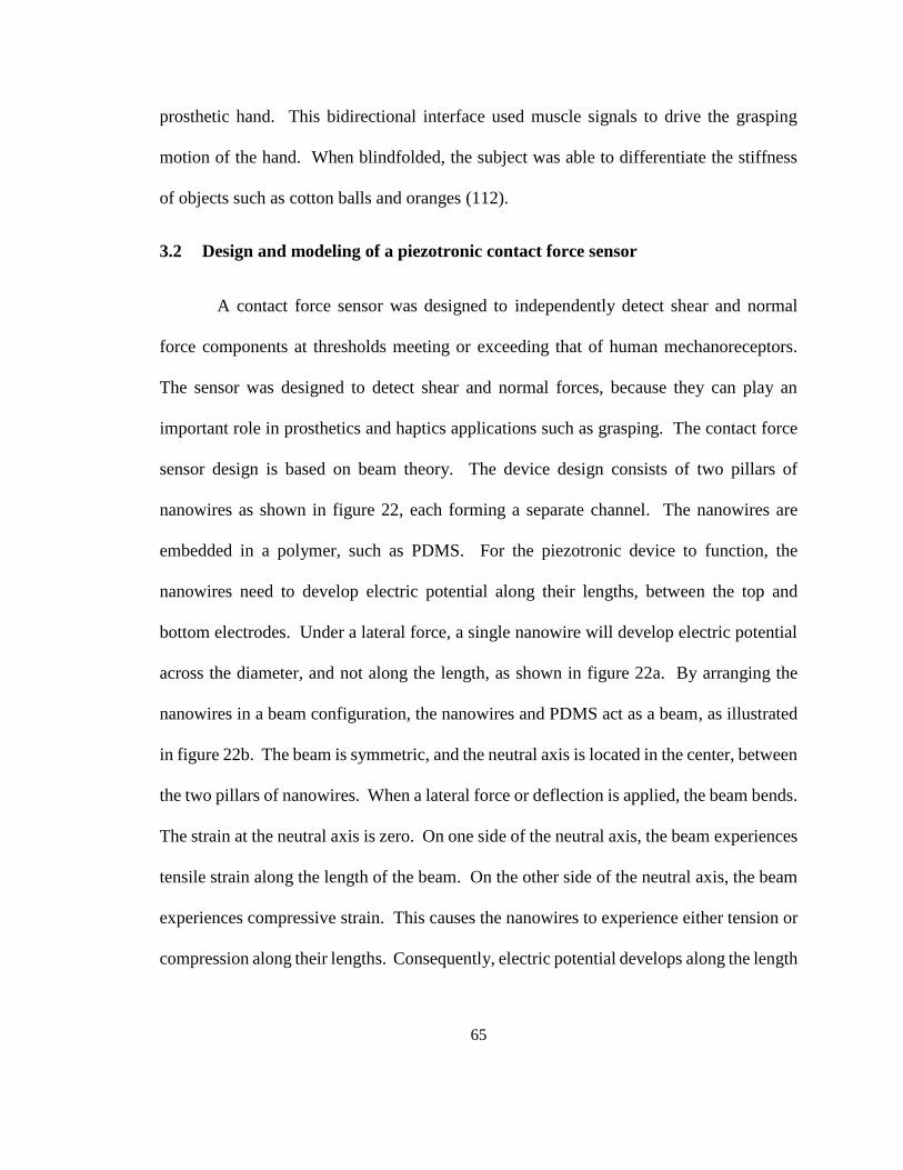
65
prosthetic hand. This bidirectional interface used muscle signals to drive the grasping
motion of the hand. When blindfolded, the subject was able to differentiate the stiffness
of objects such as cotton balls and oranges (112).
3.2 Design and modeling of a piezotronic contact force sensor
A contact force sensor was designed to independently detect shear and normal
force components at thresholds meeting or exceeding that of human mechanoreceptors.
The sensor was designed to detect shear and normal forces, because they can play an
important role in prosthetics and haptics applications such as grasping. The contact force
sensor design is based on beam theory. The device design consists of two pillars of
nanowires as shown in figure 22, each forming a separate channel. The nanowires are
embedded in a polymer, such as PDMS. For the piezotronic device to function, the
nanowires need to develop electric potential along their lengths, between the top and
bottom electrodes. Under a lateral force, a single nanowire will develop electric potential
across the diameter, and not along the length, as shown in figure 22a. By arranging the
nanowires in a beam configuration, the nanowires and PDMS act as a beam, as illustrated
in figure 22b. The beam is symmetric, and the neutral axis is located in the center, between
the two pillars of nanowires. When a lateral force or deflection is applied, the beam bends.
The strain at the neutral axis is zero. On one side of the neutral axis, the beam experiences
tensile strain along the length of the beam. On the other side of the neutral axis, the beam
experiences compressive strain. This causes the nanowires to experience either tension or
compression along their lengths. Consequently, electric potential develops along the length
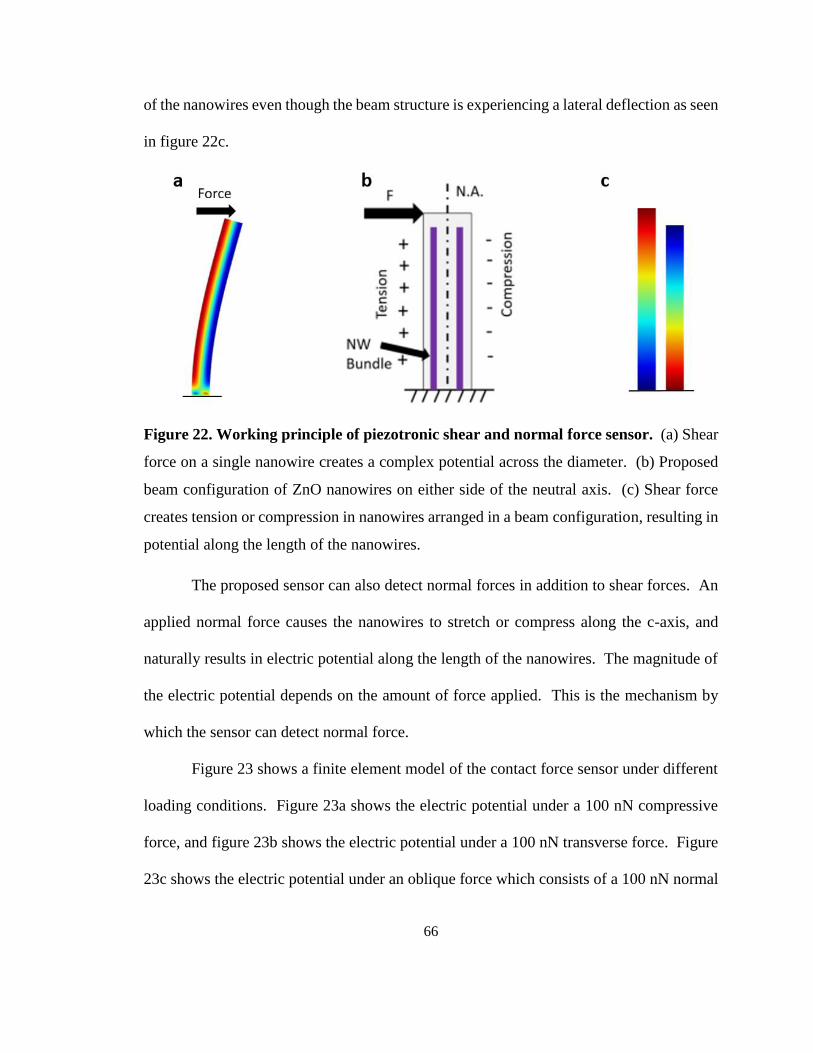
66
of the nanowires even though the beam structure is experiencing a lateral deflection as seen
in figure 22c.
Figure 22. Working principle of piezotronic shear and normal force sensor. (a) Shear
force on a single nanowire creates a complex potential across the diameter. (b) Proposed
beam configuration of ZnO nanowires on either side of the neutral axis. (c) Shear force
creates tension or compression in nanowires arranged in a beam configuration, resulting in
potential along the length of the nanowires.
The proposed sensor can also detect normal forces in addition to shear forces. An
applied normal force causes the nanowires to stretch or compress along the c-axis, and
naturally results in electric potential along the length of the nanowires. The magnitude of
the electric potential depends on the amount of force applied. This is the mechanism by
which the sensor can detect normal force.
Figure 23 shows a finite element model of the contact force sensor under different
loading conditions. Figure 23a shows the electric potential under a 100 nN compressive
force, and figure 23b shows the electric potential under a 100 nN transverse force. Figure
23c shows the electric potential under an oblique force which consists of a 100 nN normal
67
component, and a 100 nN transverse component. In all cases the bottom face of the
nanowire was set to ground potential, and the force was applied evenly to the top surface
of the sensor. In each loading case, a unique potential distribution is created in the
nanowires. The different potential distributions will result in different changes in
conductivity for each channel. The result suggests that the sensor will be able to distinguish
between the three different loading conditions. Furthermore, the signals from the normal
and transverse force components can be separated and extracted from the sensor. The
normal force component corresponds to the average of the two channels, and the shear
force component corresponds to the difference between the two channels.
Figure 23. Simulation of piezopotential in ZnO contact force sensor. (a) Piezoelectric
potential under 100 nN compressive force, (b) 100 nN transverse force, and (c) oblique
force with 100 nN components in normal and transverse directions.
68
The sensor can be expanded to measure shear force in two dimensions by creating
a 2 x 2 array of nanowire pillars (4 channels). Multiple 2 x 2 arrays can be created across
the surface of the sensor to provide sensing at a high spatial resolution. The electric
potentials created in the sensor under a 100 nN load are sufficient to generate measureable
signals, suggesting that the force detection threshold can be lower than that of a human
mechanoreceptor. Preliminary fabrication and testing results for the contact force sensor
are shown in the appendix in figure A3 and figure A4.
The application of the sensor for object slip prevention is envisioned in figure 24a.
The sensor is affixed to the finger of a prosthetic hand. The hand grasps a cup which is
being filled with water. The sensor detects the grasping force, which is the normal force
component, and the shear force, which corresponds to the weight of the cup. As the cup is
filled with water, the weight increases, along with the shear force measured by the sensor.
The grasping force of the hand is maintained by a closed-loop feedback controller. PD
controllers have been used for grasp force control, and reflect natural human force sensing,
which can detect magnitude and rate of force change (138, 139). The set-point for the
controller is the ratio of shear to normal force. A small margin may be added to this ratio
for safety. As the weight of the cup increases, the shear force increases, and the controller
will increase the normal (grasping) force to maintain the ratio. Using the ratio of shear to
normal force also has the benefit of reducing the system to a single input. The increasing
weight of the cup can be generalized to any external disturbance of the object, which
normal force sensing alone cannot account for during object slip control. The finite
element model indicates that the proposed sensor can detect shear and normal forces on the

69
order of 100 nN, which is lower than the 0.01 N threshold for sensors previously
demonstrated in slip detection applications (140).
Figure 24b illustrates another potential advantage of the shear force sensing
capability. A prosthetic hand with the sensor attached to the finger moves across a curved
surface. With normal force sensing only (top), there is only one component of the force
vector to provide information about the curvature of the surface. With normal and shear
force sensing (bottom), the measured force can be resolved into two components,
potentially providing more information about the surface. It is hypothesized that the
addition of the shear force information would result in lower detection and discrimination
thresholds for curvature changes, compared to normal-only force sensing.
Figure 24. Applications for piezotronic contact force sensor. (a) Object slip prevention
with a shear and normal force sensor. The figure depicts a proposed realization of the shear
and normal force sensor for slip prevention. The sensor is attached to a prosthetic hand
which grasps a cup as it is filled with water. The increasing weight causes an increase in
measured shear force, which signals a feedback controller to increase the normal grasping
force. (b) Extracting force components during curvature exploration from normal force
sensor (top) and combined shear and normal force sensor (bottom).
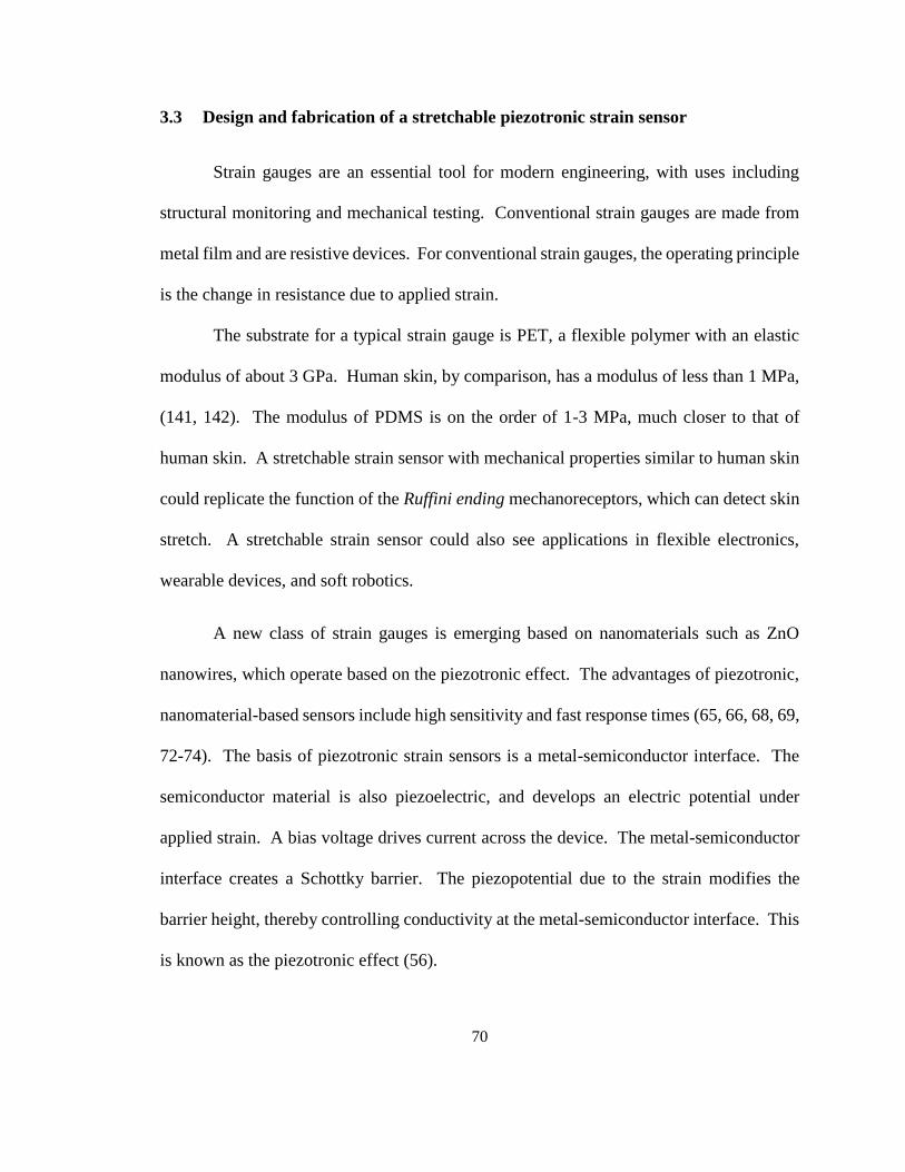
70
3.3 Design and fabrication of a stretchable piezotronic strain sensor
Strain gauges are an essential tool for modern engineering, with uses including
structural monitoring and mechanical testing. Conventional strain gauges are made from
metal film and are resistive devices. For conventional strain gauges, the operating principle
is the change in resistance due to applied strain.
The substrate for a typical strain gauge is PET, a flexible polymer with an elastic
modulus of about 3 GPa. Human skin, by comparison, has a modulus of less than 1 MPa,
(141, 142). The modulus of PDMS is on the order of 1-3 MPa, much closer to that of
human skin. A stretchable strain sensor with mechanical properties similar to human skin
could replicate the function of the Ruffini ending mechanoreceptors, which can detect skin
stretch. A stretchable strain sensor could also see applications in flexible electronics,
wearable devices, and soft robotics.
A new class of strain gauges is emerging based on nanomaterials such as ZnO
nanowires, which operate based on the piezotronic effect. The advantages of piezotronic,
nanomaterial-based sensors include high sensitivity and fast response times (65, 66, 68, 69,
72-74). The basis of piezotronic strain sensors is a metal-semiconductor interface. The
semiconductor material is also piezoelectric, and develops an electric potential under
applied strain. A bias voltage drives current across the device. The metal-semiconductor
interface creates a Schottky barrier. The piezopotential due to the strain modifies the
barrier height, thereby controlling conductivity at the metal-semiconductor interface. This
is known as the piezotronic effect (56).
71
ZnO nanowires are commonly used for piezotronic devices, and can be synthesized
using hydrothermal methods, or by chemical vapor deposition (77, 143). The advantages
of hydrothermal synthesis include scalability, and low process temperature (< 100 ⁰C)
which is compatible with polymer substrates and photolithography patterning. On the other
hand, CVD can produce longer, higher quality nanowires, but silicon substrates are
typically used as the high temperatures are not compatible with polymer substrates.
A method for mechanically transferring CVD grown ZnO nanowires was designed
to create a stretchable, conformal piezotronic strain sensor (144). The purpose of the
mechanical transfer process was to remove the ZnO nanowires from the rigid CVD growth
substrate, while simultaneously creating a new stretchable substrate. One common method
for mechanically removing nanowires from a substrate is to infiltrate the nanowires with a
polymer such as PDMS. The cured PDMS is then peeled away from the substrate along
with the nanowires (145). The transfer process can be optimized by changing the viscosity
of the PDMS, and the process works for different materials, such as silicon and gallium
phosphide (146). Mechanical transfer is possible by other processes, such as roll-transfer
printing, and has been used to fabricate ZnO nanowire FETs and silicon nanowire
electronic devices (147, 148). Many nanowire devices already use polymer infiltration to
protect the nanowire arrays, so mechanical transfer is a logical extension of the device
fabrication process (67, 82).
PET is a commonly used substrate for flexible electronics, however the relatively
high elastic modulus makes it difficult to conform to complex surfaces. By comparison,
PDMS has a relatively low elastic modulus of only a few megapascals. The mechanical
72
transfer process allows for the use of high quality, CVD grown ZnO nanowires in a
stretchable, conformal device.
Figure 25 shows the device fabrication steps for the strain sensor. Vertical, well-
aligned ZnO nanowires were grown on a silicon substrate as seen in Figure 25a. First, a 5
nm thick Cr adhesion layer was sputtered on a silicon wafer followed by a 100 nm thick
ZnO seed layer. The wafer was diced into 5 mm x 20 mm substrates. To improve the
alignment of the ZnO nanowires grown by CVD, a second seed layer was grown using a
hydrothermal recipe developed by Zhu, et al. (77). This second seed layer consists of a so
called textured film, which is a semi-merged layer of short ZnO nanowires a few microns
in length. The textured film layer was grown in a solution containing 175 mM Zinc Nitrate
and 175 mM HMTA. Substrates were floated on top of the solution with the sputtered seed
layer face down, in a convection oven for 6 hours at 95 oC. Next, ZnO nanowires were
grown on the textured film seed layer using CVD. A ceramic crucible was prepared with
600 mg of source material powder, which contained a 1:1 ratio of ZnO powder and carbon
powder by mass. The powder was spread evenly across the base of the crucible. Two
substrates with the textured film seed layer were placed face down on top of the crucible.
The crucible and substrates were placed in the tube furnace and dried for 30 minutes at 160
⁰C under vacuum (~ 50 mT). Next, argon gas was introduced at a flow rate of 30 SCCM,
and the furnace was ramped to 960 ⁰C, the growth temperature. Once the growth
temperature was reached, oxygen was introduced at 10 SCCM, and the growth proceeded
for 10 minutes at 50 Torr pressure. After the growth time, the furnace was allowed to cool

73
and the samples were removed. The growth resulted in vertical, aligned ZnO nanowires
approximately 100 µm in length.
Figure 25. Piezotronic strain sensor fabrication steps. (a) ZnO Nanowires grown by
CVD on silicon wafer with hydrothermal textured seed layer. (b) PDMS infiltrated into
nanowire array with vacuum chamber and spin coating. (c) Mechanical transfer of ZnO
nanowires and new stretchable PDMS substrate. (d) PET mask and plasma etching to
expose nanowire tips in PDMS. (e) Deposition of gold top electrode and mask removal.
(f) SEM image shows exposed nanowires on bottom of PDMS substrate following
mechanical transfer. Scale bar is 5 µm.
A layer of PDMS was drop-coated onto the CVD-grown nanowires to protect the
nanowires and act as a stretchable device substrate. Next, the samples were degassed under
vacuum. This served to remove air trapped in the nanowires, and improve infiltration of
the PDMS polymer. Excess PDMS was then spun off using a spin coater at 4,000 rpm for
2 minutes. The PDMS was cured on a hot plate at 150 ⁰C for 1 hour. Figure 25b shows
the ZnO nanowires embedded in PDMS. After curing, the PDMS layer and embedded
nanowires were mechanically removed from the silicon substrate with a razor as shown in
74
figure 25c. The removed PDMS became the new, stretchable substrate for the embedded
ZnO nanowires.
After removal from the Si wafer, the PDMS samples were flattened on a glass slide
and covered with a polymer mask made from PET. The mask had rectangular windows
approximately 2 mm x 10 mm in size which exposed a part of each sample as seen in figure
25d. Reactive Ion Etching (RIE) was used to remove PDMS from the mask windows and
expose the tips of the nanowires. The PDMS was etched for 25 minutes using 45 SCCM
SF6:15 SCCM O2. A second etch was performed for 30 seconds using oxygen plasma,
which has been shown to improve the adhesion of the top electrode and improve the quality
of the Schottky contact (14, 149, 150). After oxygen cleaning, a 5 thick nm Cr adhesion
layer and 100 nm thick Au top electrode were deposited using electron beam evaporation
(figure 25e). The etching mask and excess gold were removed, and the strain sensor was
attached to the stepped shaft with silver paint. The mechanical transfer process was
characterized with SEM imaging. The SEM image in figure 25f shows ZnO nanowires
protruding from the bottom surface of the PDMS after removal from the silicon wafer. The
silver paint formed an Ohmic contact with the exposed nanowires on the bottom of the
device, and served as the bottom electrode.
The performance of the strain sensor was tested in a structural monitoring
application, using a stepped shaft with a shoulder fillet. The shaft was 4.5 inches long,
with major and minor diameters of 0.75 and 0.5 inches, respectively. The radius of the
shoulder fillet was 0.25 inches. For the given geometry the shaft was calculated to have a
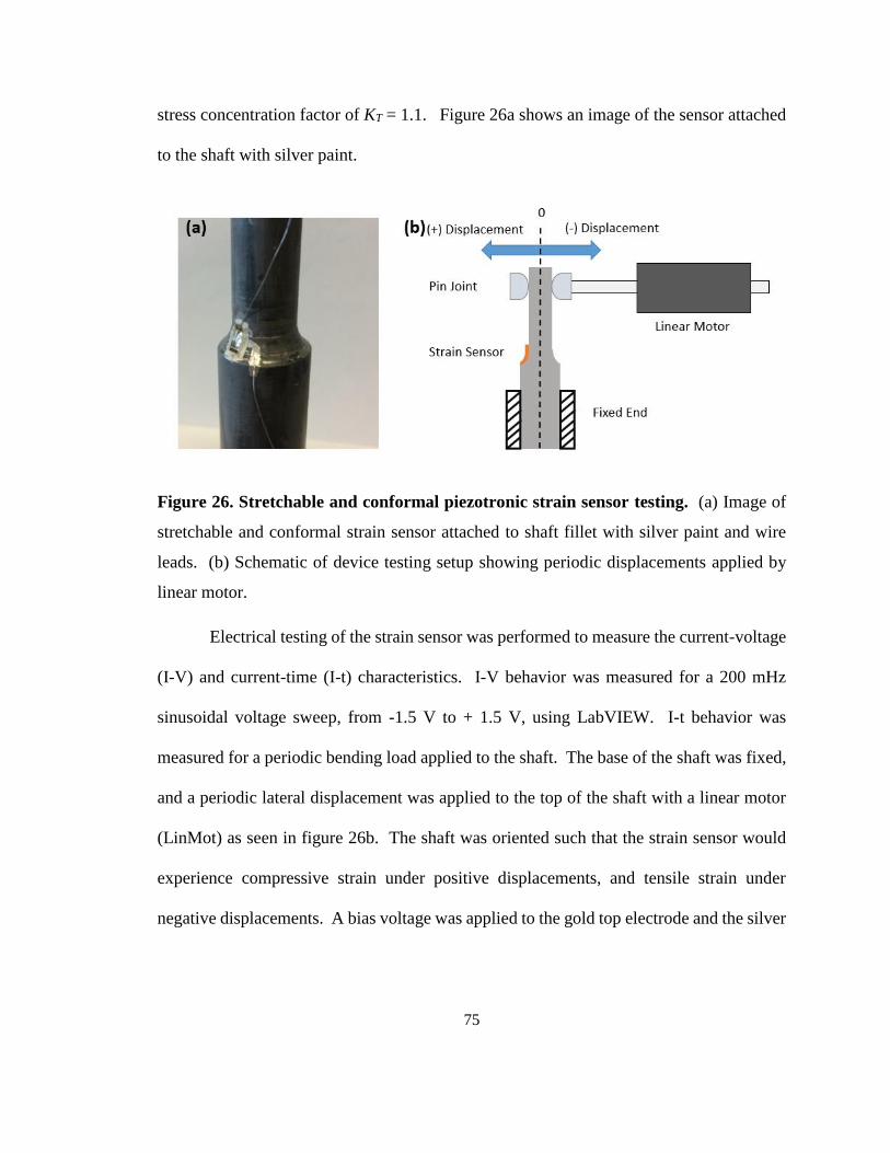
75
stress concentration factor of KT = 1.1. Figure 26a shows an image of the sensor attached
to the shaft with silver paint.
Figure 26. Stretchable and conformal piezotronic strain sensor testing. (a) Image of
stretchable and conformal strain sensor attached to shaft fillet with silver paint and wire
leads. (b) Schematic of device testing setup showing periodic displacements applied by
linear motor.
Electrical testing of the strain sensor was performed to measure the current-voltage
(I-V) and current-time (I-t) characteristics. I-V behavior was measured for a 200 mHz
sinusoidal voltage sweep, from -1.5 V to + 1.5 V, using LabVIEW. I-t behavior was
measured for a periodic bending load applied to the shaft. The base of the shaft was fixed,
and a periodic lateral displacement was applied to the top of the shaft with a linear motor
(LinMot) as seen in figure 26b. The shaft was oriented such that the strain sensor would
experience compressive strain under positive displacements, and tensile strain under
negative displacements. A bias voltage was applied to the gold top electrode and the silver
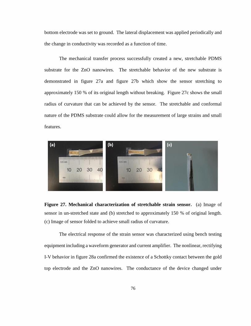
76
bottom electrode was set to ground. The lateral displacement was applied periodically and
the change in conductivity was recorded as a function of time.
The mechanical transfer process successfully created a new, stretchable PDMS
substrate for the ZnO nanowires. The stretchable behavior of the new substrate is
demonstrated in figure 27a and figure 27b which show the sensor stretching to
approximately 150 % of its original length without breaking. Figure 27c shows the small
radius of curvature that can be achieved by the sensor. The stretchable and conformal
nature of the PDMS substrate could allow for the measurement of large strains and small
features.
Figure 27. Mechanical characterization of stretchable strain sensor. (a) Image of
sensor in un-stretched state and (b) stretched to approximately 150 % of original length.
(c) Image of sensor folded to achieve small radius of curvature.
The electrical response of the strain sensor was characterized using bench testing
equipment including a waveform generator and current amplifier. The nonlinear, rectifying
I-V behavior in figure 28a confirmed the existence of a Schottky contact between the gold
top electrode and the ZnO nanowires. The conductance of the device changed under
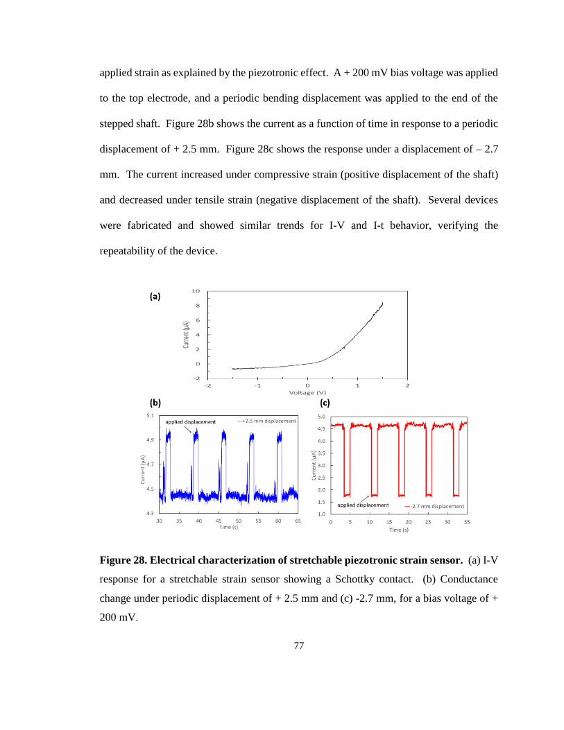
77
applied strain as explained by the piezotronic effect. A + 200 mV bias voltage was applied
to the top electrode, and a periodic bending displacement was applied to the end of the
stepped shaft. Figure 28b shows the current as a function of time in response to a periodic
displacement of + 2.5 mm. Figure 28c shows the response under a displacement of – 2.7
mm. The current increased under compressive strain (positive displacement of the shaft)
and decreased under tensile strain (negative displacement of the shaft). Several devices
were fabricated and showed similar trends for I-V and I-t behavior, verifying the
repeatability of the device.
Figure 28. Electrical characterization of stretchable piezotronic strain sensor. (a) I-V
response for a stretchable strain sensor showing a Schottky contact. (b) Conductance
change under periodic displacement of + 2.5 mm and (c) -2.7 mm, for a bias voltage of +
200 mV.
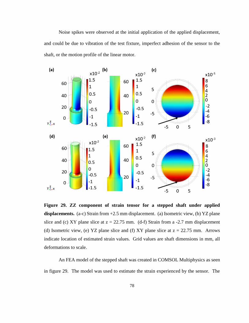
78
Noise spikes were observed at the initial application of the applied displacement,
and could be due to vibration of the test fixture, imperfect adhesion of the sensor to the
shaft, or the motion profile of the linear motor.
Figure 29. ZZ component of strain tensor for a stepped shaft under applied
displacements. (a-c) Strain from +2.5 mm displacement. (a) Isometric view, (b) YZ plane
slice and (c) XY plane slice at z = 22.75 mm. (d-f) Strain from a -2.7 mm displacement
(d) Isometric view, (e) YZ plane slice and (f) XY plane slice at z = 22.75 mm. Arrows
indicate location of estimated strain values. Grid values are shaft dimensions in mm, all
deformations to scale.
An FEA model of the stepped shaft was created in COMSOL Multiphysics as seen
in figure 29. The model was used to estimate the strain experienced by the sensor. The
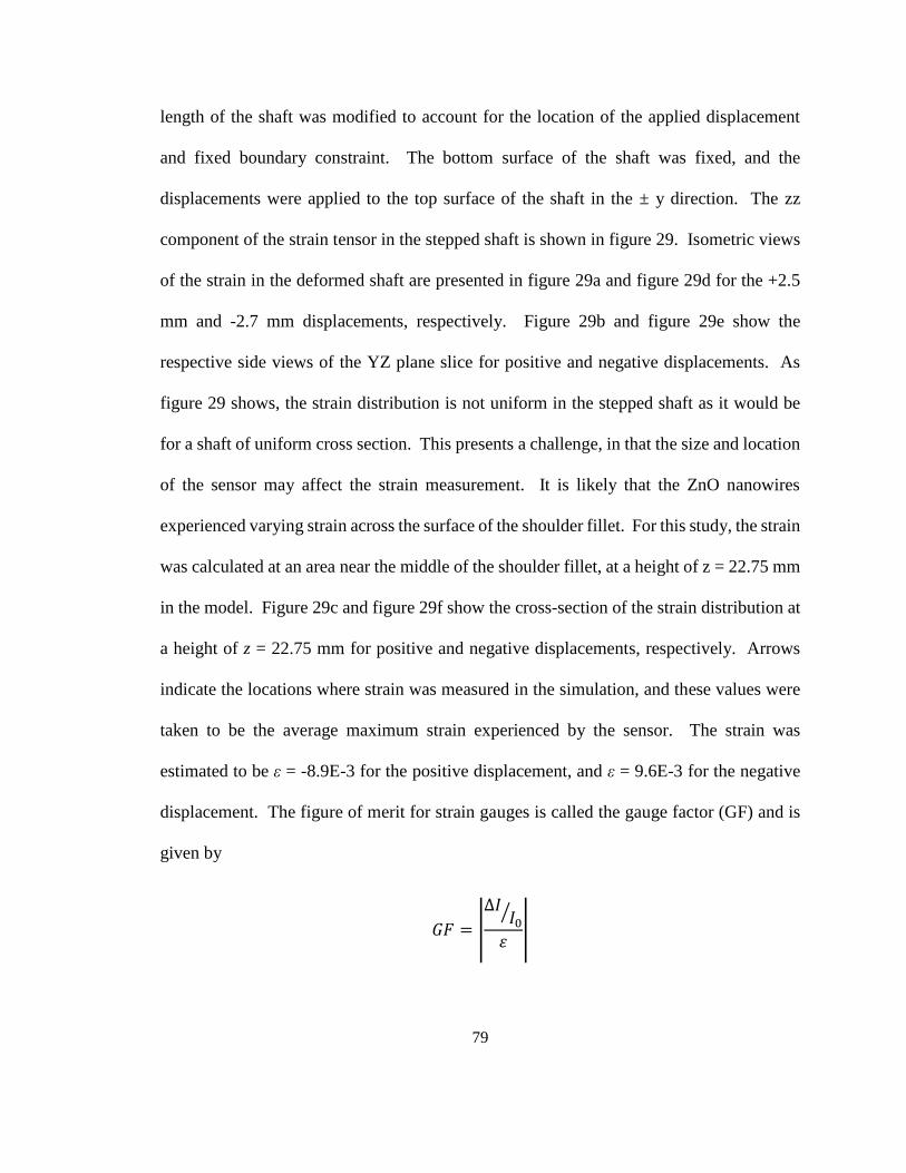
79
length of the shaft was modified to account for the location of the applied displacement
and fixed boundary constraint. The bottom surface of the shaft was fixed, and the
displacements were applied to the top surface of the shaft in the ± y direction. The zz
component of the strain tensor in the stepped shaft is shown in figure 29. Isometric views
of the strain in the deformed shaft are presented in figure 29a and figure 29d for the +2.5
mm and -2.7 mm displacements, respectively. Figure 29b and figure 29e show the
respective side views of the YZ plane slice for positive and negative displacements. As
figure 29 shows, the strain distribution is not uniform in the stepped shaft as it would be
for a shaft of uniform cross section. This presents a challenge, in that the size and location
of the sensor may affect the strain measurement. It is likely that the ZnO nanowires
experienced varying strain across the surface of the shoulder fillet. For this study, the strain
was calculated at an area near the middle of the shoulder fillet, at a height of z = 22.75 mm
in the model. Figure 29c and figure 29f show the cross-section of the strain distribution at
a height of z = 22.75 mm for positive and negative displacements, respectively. Arrows
indicate the locations where strain was measured in the simulation, and these values were
taken to be the average maximum strain experienced by the sensor. The strain was
estimated to be ε = -8.9E-3 for the positive displacement, and ε = 9.6E-3 for the negative
displacement. The figure of merit for strain gauges is called the gauge factor (GF) and is
given by
𝐺𝐹 = |
∆𝐼𝐼0⁄
𝜀|

80
where I0 is the initial current without strain, ΔI is the change in current due to strain, and ε
is the applied strain. For the -2.7 mm displacement, the gauge factor was calculated to be
64. This value is comparable to a similarly conformal ZnO/carbon fiber fabric piezotronic
strain sensor with a gauge factor of 81 (72). A conventional metal strain gauge, for
comparison, has a GF of only about 2 (80). The gauge factor of the stretchable strain sensor
can likely be increased by improving the adhesion, and therefore the load transfer, between
the sensor and measured structure. The properties of the stretchable polymer used for the
substrate may also affect the sensitivity. While the low modulus PDMS substrate might
reduce the strain sensitivity on rigid structures, this tradeoff allows for measurements on
complex surfaces such as stress concentrators. Strain gauges operating under the
piezotronic effect have the potential for even higher sensitivity, as evidenced by Zhang et
al., who achieved a gauge factor of 1813 for a similar flexible, but not stretchable, ZnO
strain sensor (67).
Future work includes challenges such as improving strain transfer between the
structure and strain gauge. Strain transfer performance is affected by adhesive properties
(151). The silver paint used as the bottom electrode also acted as an adhesive, but was
susceptible to voids and delamination. The PDMS substrates also tended to curl up after
being removed from the silicon wafer, contributing to delamination. Despite these
challenges, there are advantages of working with stretchable polymer substrates. Soft,
stretchable strain sensors can conform to complex shapes, are mechanically compatible
with biological tissue, and have little impact on the rigidity and strain in the measured part.

81
The high sensitivity enabled by the piezotronic effect allows for strain measurement on
rigid surfaces, despite the relatively low modulus of the PDMS substrate.
3.4 Chapter summary
Due to the high sensitivity and high spatial resolution, piezotronic force sensors are
ideal for replicating human tactile perception in applications such as prosthetics and
haptics. Finite element modeling validated the design of a contact force sensor capable of
detecting shear and normal forces, at thresholds exceeding human force perception. The
proposed piezotronic shear and normal force sensor could have applications in prosthetics
and haptics for object grasping and shape perception.
Mechanical transfer of CVD grown ZnO nanowires allowed for the creation of a
stretchable and conformal strain sensor on a PDMS substrate. The ZnO/Au electrode
interface formed a Schottky contact, which is responsible for the nonlinear I-V response
and high sensitivity of piezotronic devices. Applied strains generated piezopotentials in
the ZnO nanowires, which altered the Schottky barrier height and changed the conductivity
in accordance with the piezotronic effect. The piezotronic strain sensor successfully
measured the strain on the shoulder fillet of a stepped shaft, and achieved a gauge factor of
64, higher than that of a conventional metal strain sensor. The strain sensor responded to
both positive and negative strains, and could be used to monitor strain on a rotating shaft
under reversed loading conditions. The sensor can conform to complex surfaces, and the
low modulus PDMS substrate is mechanically compatible with other stretchable materials,
such as human skin. With further development, the sensor could see use in applications
such as smart bandages and biomechanics monitoring.
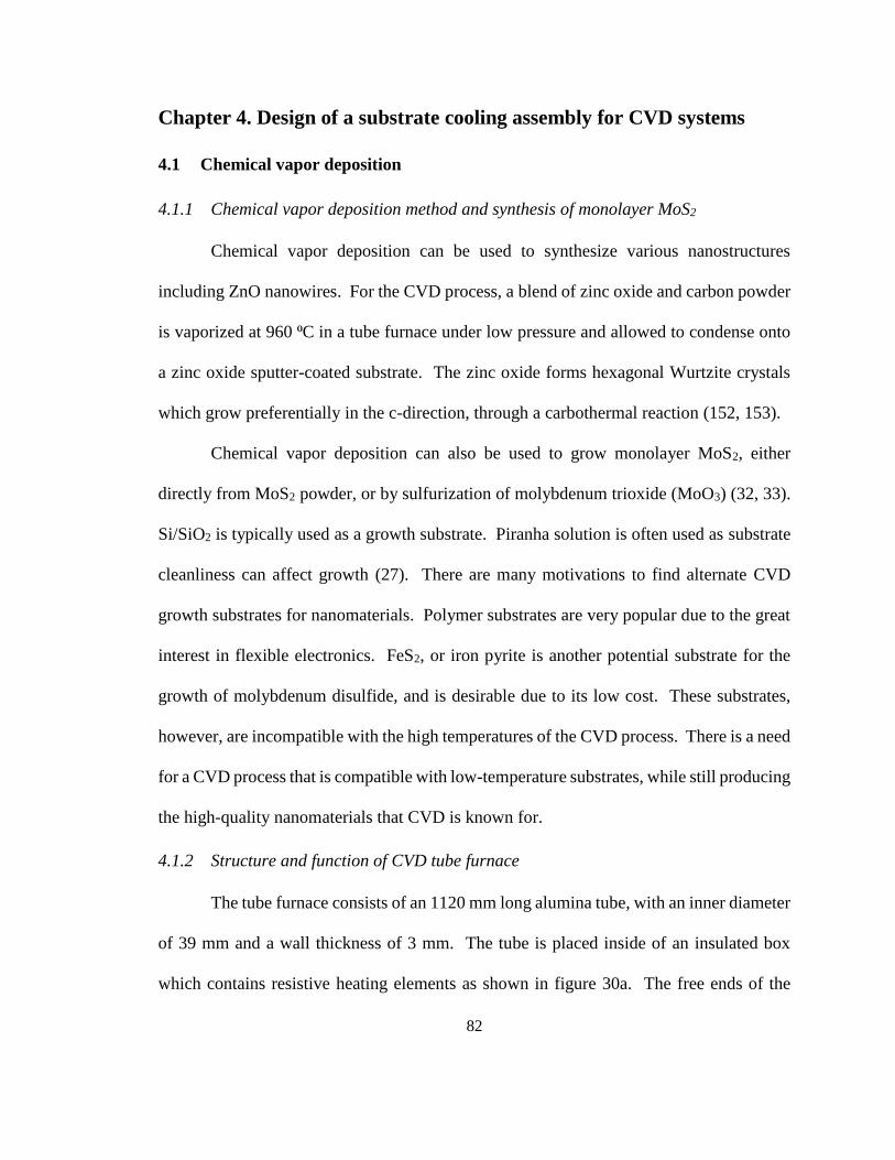
82
Chapter 4. Design of a substrate cooling assembly for CVD systems
4.1 Chemical vapor deposition
4.1.1 Chemical vapor deposition method and synthesis of monolayer MoS2
Chemical vapor deposition can be used to synthesize various nanostructures
including ZnO nanowires. For the CVD process, a blend of zinc oxide and carbon powder
is vaporized at 960 ⁰C in a tube furnace under low pressure and allowed to condense onto
a zinc oxide sputter-coated substrate. The zinc oxide forms hexagonal Wurtzite crystals
which grow preferentially in the c-direction, through a carbothermal reaction (152, 153).
Chemical vapor deposition can also be used to grow monolayer MoS2, either
directly from MoS2 powder, or by sulfurization of molybdenum trioxide (MoO3) (32, 33).
Si/SiO2 is typically used as a growth substrate. Piranha solution is often used as substrate
cleanliness can affect growth (27). There are many motivations to find alternate CVD
growth substrates for nanomaterials. Polymer substrates are very popular due to the great
interest in flexible electronics. FeS2, or iron pyrite is another potential substrate for the
growth of molybdenum disulfide, and is desirable due to its low cost. These substrates,
however, are incompatible with the high temperatures of the CVD process. There is a need
for a CVD process that is compatible with low-temperature substrates, while still producing
the high-quality nanomaterials that CVD is known for.
4.1.2 Structure and function of CVD tube furnace
The tube furnace consists of an 1120 mm long alumina tube, with an inner diameter
of 39 mm and a wall thickness of 3 mm. The tube is placed inside of an insulated box
which contains resistive heating elements as shown in figure 30a. The free ends of the
83
ceramic tube extend out of the box on each end for a length of approximately 150 mm. The
furnace can reach temperatures up to 1200 ⁰C, and can be programmed to perform ramps
and dwells at various temperatures. Two thermocouples measure the temperature at the
center of the furnace, and the set-point is maintained by a controller.
Each end of the furnace is closed by a custom fabricated stainless steel endcap. The
endcaps circulate chilled water around the exposed ends of the furnace tube for safety, and
to protect the rubber gaskets that seal the tube. The upstream endcap is connected to a gas
supply line which allows carrier and reaction gases such as argon and oxygen to enter the
furnace. Gas flow rates are controlled by mass flow controllers. The downstream endcap
is connected to a vacuum pump or vented directly to the fume hood. The endcaps provide
a vacuum seal using rubber gaskets. The vacuum pump can achieve approximately 20 mT
of pressure. Chilled water is provided to the furnace by an overhead manifold connected
to the building chilled water supply. Figure 30b shows an experimental setup for CVD
growth of ZnO nanowires, and figure 30c shows an image of the furnace during operation.
The controller maintains the furnace set-point temperature at the center of the tube
furnace. Away from the center, the temperature decreases. Different source materials can
be heated to different temperatures in the furnace by placing them at the appropriate
position in the furnace. In order to determine the positon to place the materials, the
temperature as a function of position was measured.
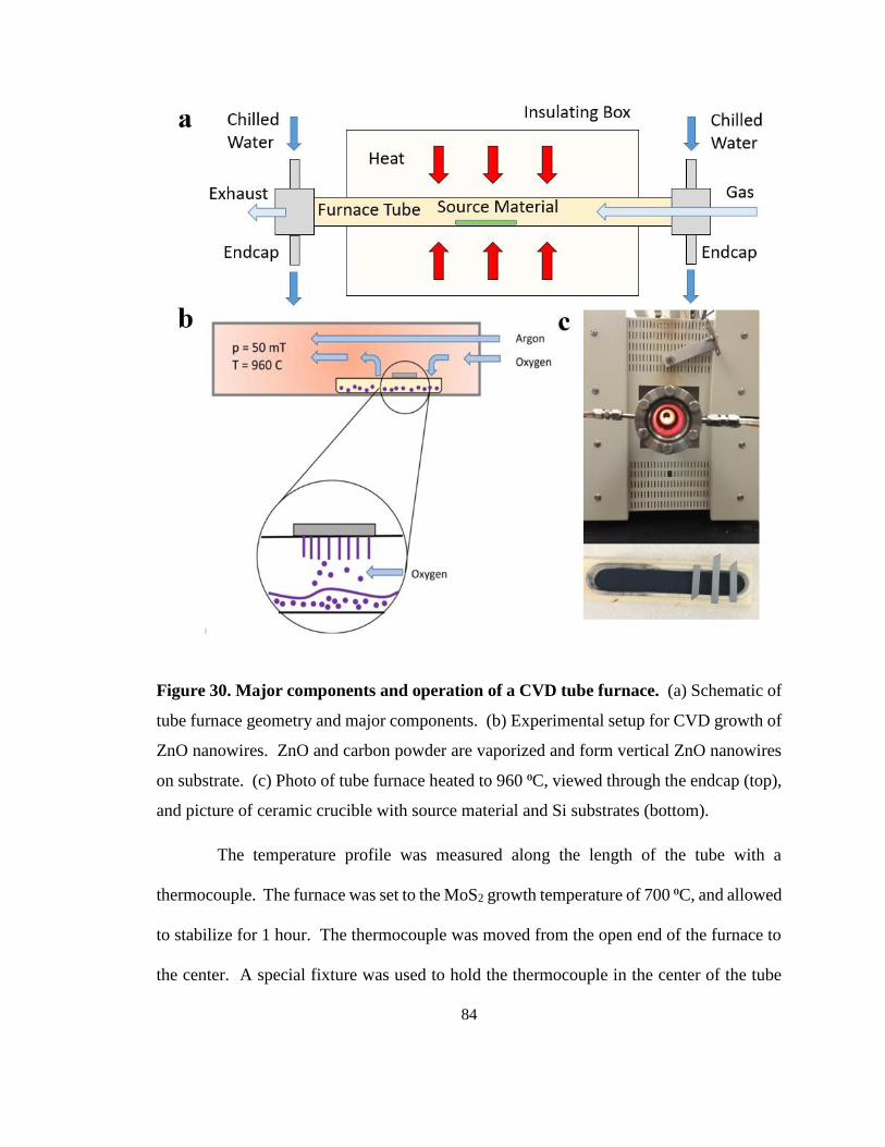
84
Figure 30. Major components and operation of a CVD tube furnace. (a) Schematic of
tube furnace geometry and major components. (b) Experimental setup for CVD growth of
ZnO nanowires. ZnO and carbon powder are vaporized and form vertical ZnO nanowires
on substrate. (c) Photo of tube furnace heated to 960 ⁰C, viewed through the endcap (top),
and picture of ceramic crucible with source material and Si substrates (bottom).
The temperature profile was measured along the length of the tube with a
thermocouple. The furnace was set to the MoS2 growth temperature of 700 ⁰C, and allowed
to stabilize for 1 hour. The thermocouple was moved from the open end of the furnace to
the center. A special fixture was used to hold the thermocouple in the center of the tube
85
diameter, away from the walls. The temperature was recorded at 10 mm intervals, and the
thermocouple was held at each location for a short time until the temperature measurement
stabilized. Results for the temperature profile as a function of position in the tube furnace
are presented in figure 31.
Figure 31. Temperature profile in a CVD tube furnace. The furnace was set to 700 ⁰C.
Temperatures were measured at various distances from the center of the tube, in mm.
Temperature profile is for ½ of the tube length.
4.2 CVD substrate cooling assembly design
One of the major limitations of chemical vapor deposition is the high temperatures
involved. These high temperatures are necessary for vaporizing the source material for the
chemical reaction, but are incompatible with many substrates such as polymers. CVD can
produce high quality nanomaterials that cannot currently be achieved by other means.
86
There is widespread and growing interest in flexible electronics on polymer substrates, and
these devices can benefit the high quality nanomaterials grown by CVD. Additionally,
patterning of nanomaterials is very important for creating multi-channel devices and other
reasons. Such patterning is often achieved by photolithography, a microfabrication
techniques which uses UV sensitive polymers. Nanomaterial synthesis commonly relies
on so called epitaxial seed layers. In other words, the crystal structure of the seed layer
must match the crystal structure of the nanomaterial. Epitaxial seed layer materials can be
expensive, however. Alternative seed layers with a near-epitaxial match can be much more
affordable, but may not be compatible with high temperatures.
The CVD furnace provides a wide ranging, location-dependent temperature profile.
However, at present, a single location cannot provide both the high temperature needed for
the reaction, and the low temperature needed for certain substrates. The goal of this project
was to develop a cooling assembly which can provide localized cooling to a substrate
placed in the high-temperature region of the furnace.
The substrate cooling apparatus must meet multiple design requirements. First, the
assembly must provide sufficient localized cooling to the substrate without reducing the
high temperature near the source material. There must be sufficient clearance between the
inner wall of the tube furnace and the cooling assembly to avoid conductive heat transfer.
Finally, the apparatus must survive the high temperature chemical environment inside the
tube furnace.
The assembly achieves localized cooling of the substrate by circulating chilled
water inside of the furnace. The overriding design constraint was the geometry of the tube
87
furnace. The tube furnace has an inner dimeter of 39 mm, and must contain the cooling
assembly and room for a ceramic crucible to hold the source material. Within this size
envelope, the design was optimized to maximize several objectives. First, the diameter of
the tubes which deliver and remove the chilled water was maximized to deliver the highest
volume of water. Second, the volume of chilled water was maximized in the immediate
vicinity of the substrate. Third, the diameter of the sample stage was maximized to
accommodate the largest sample possible. Fourth, the assembly was designed to allow for
a wide adjustment of sample height. The sample height refers to the vertical distance from
the source material to the substrate. A layer of insulation was wrapped around the chilled
water tubes, and the thickness of the insulation was maximized. Finally, the assembly was
designed to use standard tube stock sizes whenever possible to minimize cost and lead time.
Figure 32. Major components of CVD cooling assembly. Major assembly components
are numbered. Item 7 is the sample cooling chamber, items 1, 2, and 3 are the insulating
sleeves, and item 5 is the endcap. Items 8 and 9 are the chilled water inlet and outlet tubes.

88
The assembly was designed with type 304 stainless steel for corrosion resistance.
Wall thicknesses for the tubes ranged from 0.02 inches to 0.12 inches. The maximum
temperature of the steel is 1500 ⁰F, or 815 ⁰C, which is above the synthesis temperature for
MoS2. The furnace consists of three main components, which are shown in figure 32. The
sample cooling chamber is a cylindrical chamber in which the substrate is placed. Cooling
water circulates around the outside of the chamber, and a layer of insulating silica fabric
surrounds the cooling water. The silica fabric was 0.054 inches thick, and has a maximum
temperature of 980 ⁰C. The entire sample stage is enclosed in 304 stainless steel. The
sample sits on a stainless steel, grated platform. The inside of the chamber is threaded, and
the sample platform can be adjusted up and down to change the distance from the substrate
to the source material. Chilled water is delivered to the substrate chamber by a long tube
leading into the furnace, and a second tube removes the circulated, heated water. Figure
33 details the design of the sample cooling chamber. An assembly view of the chamber is
shown in figure 33a, while figure 33b and figure 33c show cutaway drawings. Figure 33d
shows the adjustable height substrate stage.
89
Figure 33. Detailed view of sample cooling chamber. Individual drawing items are
numbered. (a) Assembly diagram of sample cooling chamber components. (b) Top view
of drawing item 23, showing separated cold water inlet and hot water outlet. Chilled water
circulates around substrate. (c) Side cutaway view of sample cooling chamber. Substrate
sits on height-adjustable sample stage (item 10). Silica insulation fabric and water
compartment are shown. (d) View of sample stage with external threads for height
adjustment.
The second component is a series of insulating sleeves which surround the inlet and
outlet cooling water tubes. The sleeves consist of an outer cylinder made of stainless steel,
and two inner cylinders which slide over the cooling water tubes. The sleeves are packed
with silica insulating fabric, and welded closed. There are three sleeves total, each
approximately 185 mm in length. The first sleeve is permanently attached to the sample
cooling chamber. The additional two sleeves may be slid on to the assembly to adjust the
length. One, two, or three sleeves may be used. The number of sleeves determines the
length of the cooling assembly, and the horizontal position of the substrate in the tube
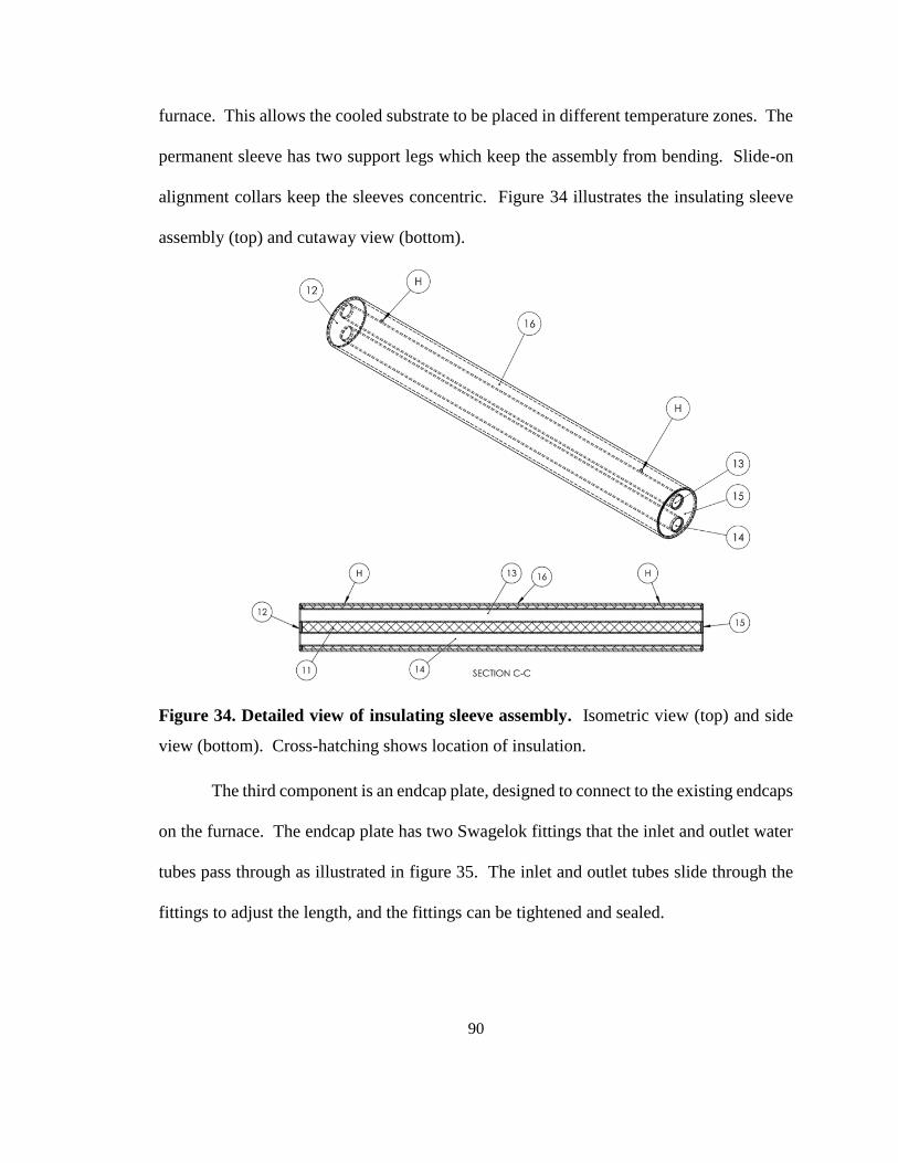
90
furnace. This allows the cooled substrate to be placed in different temperature zones. The
permanent sleeve has two support legs which keep the assembly from bending. Slide-on
alignment collars keep the sleeves concentric. Figure 34 illustrates the insulating sleeve
assembly (top) and cutaway view (bottom).
Figure 34. Detailed view of insulating sleeve assembly. Isometric view (top) and side
view (bottom). Cross-hatching shows location of insulation.
The third component is an endcap plate, designed to connect to the existing endcaps
on the furnace. The endcap plate has two Swagelok fittings that the inlet and outlet water
tubes pass through as illustrated in figure 35. The inlet and outlet tubes slide through the
fittings to adjust the length, and the fittings can be tightened and sealed.
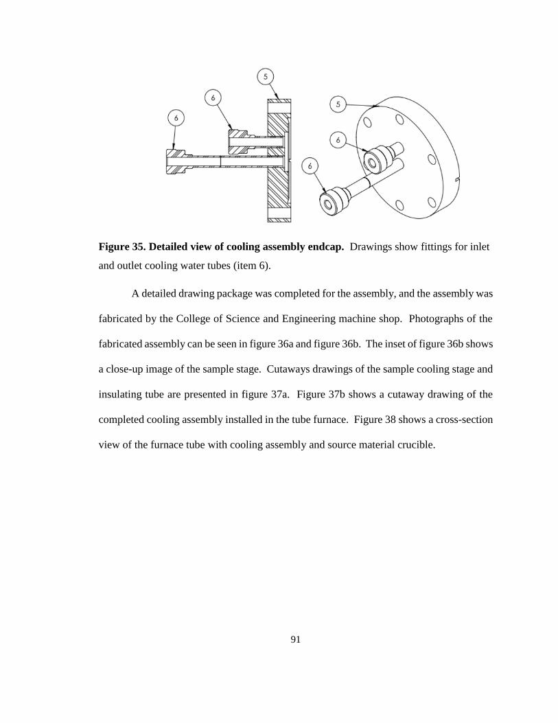
91
Figure 35. Detailed view of cooling assembly endcap. Drawings show fittings for inlet
and outlet cooling water tubes (item 6).
A detailed drawing package was completed for the assembly, and the assembly was
fabricated by the College of Science and Engineering machine shop. Photographs of the
fabricated assembly can be seen in figure 36a and figure 36b. The inset of figure 36b shows
a close-up image of the sample stage. Cutaways drawings of the sample cooling stage and
insulating tube are presented in figure 37a. Figure 37b shows a cutaway drawing of the
completed cooling assembly installed in the tube furnace. Figure 38 shows a cross-section
view of the furnace tube with cooling assembly and source material crucible.
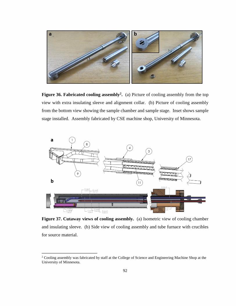
92
Figure 36. Fabricated cooling assembly2. (a) Picture of cooling assembly from the top
view with extra insulating sleeve and alignment collar. (b) Picture of cooling assembly
from the bottom view showing the sample chamber and sample stage. Inset shows sample
stage installed. Assembly fabricated by CSE machine shop, University of Minnesota.
Figure 37. Cutaway views of cooling assembly. (a) Isometric view of cooling chamber
and insulating sleeve. (b) Side view of cooling assembly and tube furnace with crucibles
for source material.
2 Cooling assembly was fabricated by staff at the College of Science and Engineering Machine Shop at the
University of Minnesota.
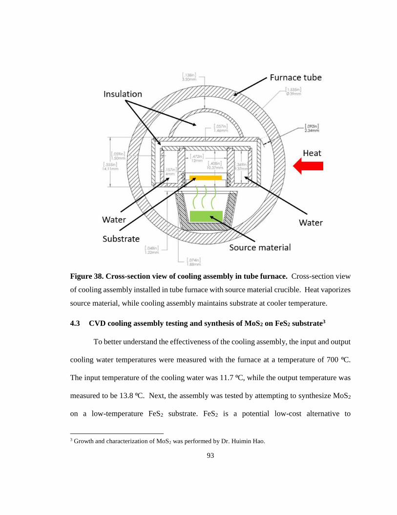
93
Figure 38. Cross-section view of cooling assembly in tube furnace. Cross-section view
of cooling assembly installed in tube furnace with source material crucible. Heat vaporizes
source material, while cooling assembly maintains substrate at cooler temperature.
4.3 CVD cooling assembly testing and synthesis of MoS2 on FeS2 substrate3
To better understand the effectiveness of the cooling assembly, the input and output
cooling water temperatures were measured with the furnace at a temperature of 700 ⁰C.
The input temperature of the cooling water was 11.7 ⁰C, while the output temperature was
measured to be 13.8 ⁰C. Next, the assembly was tested by attempting to synthesize MoS2
on a low-temperature FeS2 substrate. FeS2 is a potential low-cost alternative to
3 Growth and characterization of MoS2 was performed by Dr. Huimin Hao.

94
conventional growth substrates, but will decompose at typical MoS2 synthesis
temperatures. A schematic of the synthesis process is shown in figure 39. A small piece
of FeS2 was broken from a larger sample shown in figure 40. The FeS2 substrate was
placed in the cooling assembly. Ceramic plates with source materials (MoO3 and Sulfur
powder) were placed in the 700 ⁰C and 200 ⁰C regions of the furnace, respectively. After
the growth recipe was completed, the FeS2 substrate was removed. SEM investigation
showed MoS2 nanostructures on the FeS2 substrate as shown in figure 41. The FeS2
substrate was not visibly damaged by the high temperature, suggesting that the cooling
assembly is effective for protecting low-temperature substrates.
Figure 39. Schematic of MoS2 growth in tube furnace with CVD cooling assembly.
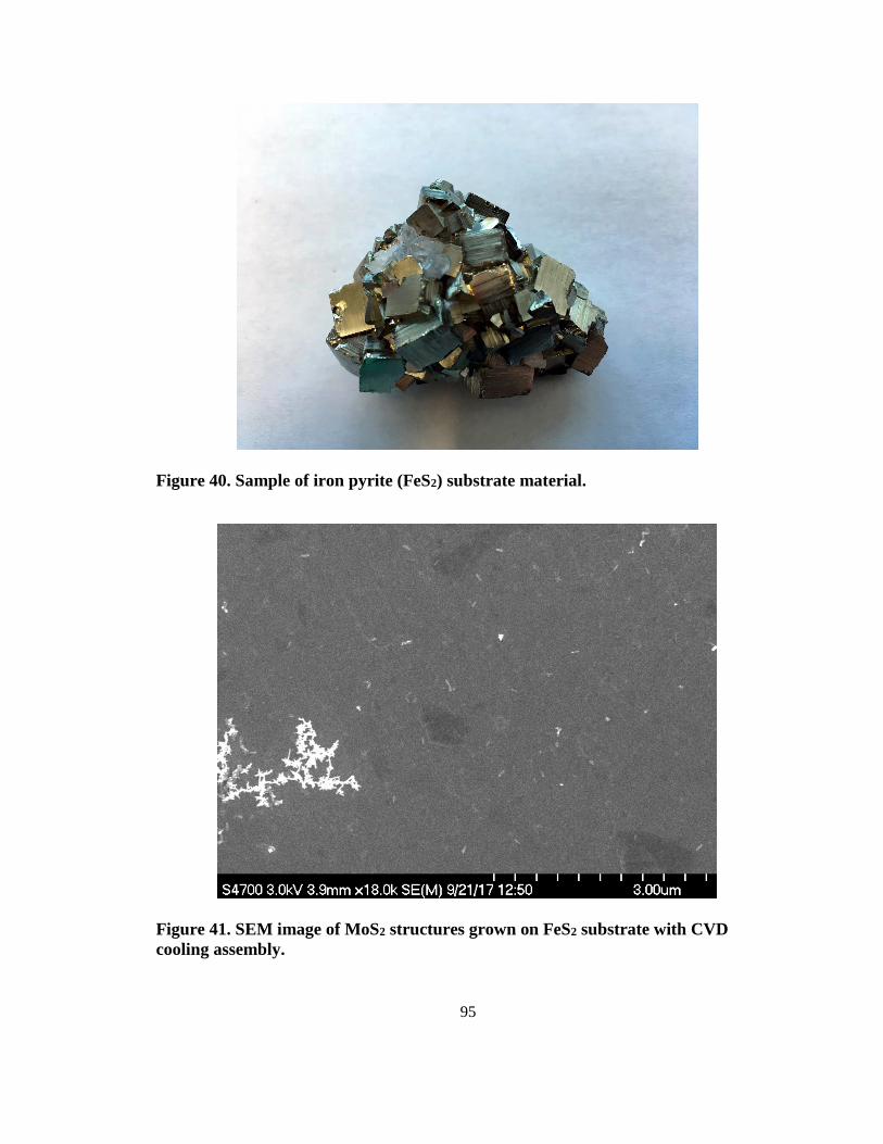
95
Figure 40. Sample of iron pyrite (FeS2) substrate material.
Figure 41. SEM image of MoS2 structures grown on FeS2 substrate with CVD
cooling assembly.
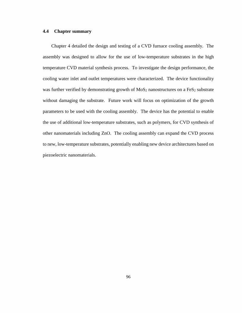
96
4.4 Chapter summary
Chapter 4 detailed the design and testing of a CVD furnace cooling assembly. The
assembly was designed to allow for the use of low-temperature substrates in the high
temperature CVD material synthesis process. To investigate the design performance, the
cooling water inlet and outlet temperatures were characterized. The device functionality
was further verified by demonstrating growth of MoS2 nanostructures on a FeS2 substrate
without damaging the substrate. Future work will focus on optimization of the growth
parameters to be used with the cooling assembly. The device has the potential to enable
the use of additional low-temperature substrates, such as polymers, for CVD synthesis of
other nanomaterials including ZnO. The cooling assembly can expand the CVD process
to new, low-temperature substrates, potentially enabling new device architectures based on
piezoelectric nanomaterials.
97
Chapter 5. Conclusions
The inherent electromechanical coupling and unique properties found in
piezoelectric nanomaterials make them well suited for many applications such as
mechanical energy harvesting, and force or strain sensing. Despite great progress, there
are barriers to the continued development of new piezoelectric nanomaterial devices. First,
there is a limited understanding of piezoelectric behavior in emerging nanomaterials, and
second, there are limitations of current fabrication techniques. This thesis explored these
challenges through finite element modeling and the expansion of current fabrication
techniques in order to realize new piezoelectric nanomaterial devices.
First, chapter 2 explored piezoelectric behavior in diphenylalanine (FF) peptide, a
new bio-inspired piezoelectric material, interesting for its promising electromechanical
properties and sustainable synthesis. Using emerging material properties, a finite element
model of a single nanowire was created to compare the piezoelectric behavior of FF peptide
and conventional piezoelectric materials. The nanowire model predicted that FF peptide
could generate significantly higher voltages than conventional piezoelectric nanomaterials
under the same applied force. Next, a 2D model of a flexible FF peptide nanogenerator
was created to predict the device performance. Synthesis of FF peptide microrods was
achieved on a polymer substrate, and the first flexible piezoelectric FF peptide
nanogenerator was realized. The device was fabricated and characterized, and the
measured output validated the finite element model. Finite element modeling can
successfully predict the piezoelectric behavior of FF peptide, and the development of FF
98
peptide devices on flexible substrates can enable new applications such as wearable devices
and flexible electronics.
Next, chapter 3 explored a special class of piezoelectric nanomaterials, those with
semiconducting properties, or so called piezotronic nanomaterials. The semiconducting
properties of ZnO nanowires make them well-suited for highly sensitive force and strain
sensors enabled by the piezotronic effect. Finite element modeling was used to explore a
new design for a piezotronic force sensor for haptics and prosthetics applications. Based
on beam theory, the design was predicted to detect shear and normal contact forces, and
was predicted to exceed the sensitivity of human mechanoreceptors. Ultralong ZnO
nanowires, such as those needed for the previous contact force sensor, are produced by
chemical vapor deposition. However, the high-temperature process is incompatible with
flexible polymers and other low-temperature substrates, which limits device design. A
mechanical transfer technique was expanded to CVD grown ZnO nanowires in order to
create a new stretchable piezotronic strain sensor on a soft polymer substrate. The gauge
factor, or sensitivity of the strain sensor exceeded that of conventional metal strain gauges.
Finite element modeling is an important tool for predicting the performance of piezotronic
nanomaterial devices, and new device architectures can be realized by expanding current
fabrication techniques to new materials and substrates.
Lastly, chapter 4 investigated the design of new process equipment to enable
synthesis of piezoelectric nanomaterials on new substrates. MoS2 is an emerging 2D
piezoelectric nanomaterial that, like ZnO, is synthesized by chemical vapor deposition.
FeS2 substrates are a potential low-cost alternative to conventional substrates, but are
99
incompatible with the high temperatures needed to produce MoS2 by CVD. An apparatus
was designed to allow for the use of low-temperature substrates inside a high-temperature
CVD furnace. The assembly delivered chilled water inside of the furnace to provide
localized cooling for the growth substrates. The cooling system was successfully used to
synthesize MoS2 on low-temperature FeS2 substrates in a CVD furnace. The cooling
assembly can potentially be used for the synthesis of other piezoelectric nanomaterials and
soft polymer substrates, further expanding the use of CVD and allowing new device
architectures to be realized.
Piezoelectric nanomaterials are the basis for many types of devices including
sensors and energy harvesters. Continued development of these devices will require further
exploration of piezoelectric behavior in emerging nanomaterials. The expansion of current
fabrication techniques is needed to enable broader synthesis of these materials and to
realize new device architectures. New devices enabled by piezoelectric nanomaterials can
help to address challenges in sustainable energy, human health, and beyond.
100
References
1. Zhu R, Jenkins K, Yang R. Degradation and nano-patterning of ferroelectric P (VDF-TrFE) thin films with electron irradiation. RSC Advances. 2015;5(129):106700-5. 2. Kholkin A, Amdursky N, Bdikin I, Gazit E, Rosenman G. Strong piezoelectricity in bioinspired peptide nanotubes. Acs Nano. 2010;4(2):610-4. 3. Wu W, Wang L, Li Y, Zhang F, Lin L, Niu S, et al. Piezoelectricity of single-atomic-layer MoS2 for energy conversion and piezotronics. Nature. 2014;514(7523):470-4. 4. Madou MJ. Fundamentals of microfabrication: the science of miniaturization: CRC press; 2002. 5. Görbitz CH. The structure of nanotubes formed by diphenylalanine, the core recognition motif of Alzheimer's β-amyloid polypeptide. Chemical communications. 2006(22):2332-4. 6. Vayssieres L. Growth of arrayed nanorods and nanowires of ZnO from aqueous solutions. Advanced Materials. 2003;15(5):464-6. 7. Mak KF, Lee C, Hone J, Shan J, Heinz TF. Atomically thin MoS(2): a new direct-gap semiconductor. Phys Rev Lett. 2010;105(13):136805. 8. Wang ZL. ZnO nanowire and nanobelt platform for nanotechnology. Materials Science and Engineering: R: Reports. 2009;64(3-4):33-71. 9. Agrawal R, Peng B, Gdoutos EE, Espinosa HD. Elasticity size effects in ZnO nanowires− a combined experimental-computational approach. Nano Letters. 2008;8(11):3668-74. 10. Morkoç H, Özgür Ü. Zinc oxide : fundamentals, materials and device technology. Weinheim: Wiley-VCH; 2009. xi, 477 p. p. 11. Wang X, Song J, Liu J, Wang ZL. Direct-current nanogenerator driven by ultrasonic waves. Science. 2007;316(5821):102-5. 12. Xu S, Wei Y, Liu J, Yang R, Wang ZL. Integrated multilayer nanogenerator fabricated using paired nanotip-to-nanowire brushes. Nano letters. 2008;8(11):4027-32. 13. Ozgur U, Alivov YI, Liu C, Teke A, Reshchikov MA, Dogan S, et al. A comprehensive review of ZnO materials and devices. Journal of Applied Physics. 2005;98(4):041301. 14. Brillson LJ, Lu Y. ZnO Schottky barriers and Ohmic contacts. Journal of Applied Physics. 2011;109(12):121301. 15. Gao Z, Zhou J, Gu Y, Fei P, Hao Y, Bao G, et al. Effects of piezoelectric potential on the transport characteristics of metal-ZnO nanowire-metal field effect transistor. J Appl Phys. 2009;105(11):113707. 16. Gao Y, Wang ZL. Electrostatic potential in a bent piezoelectric nanowire. The fundamental theory of nanogenerator and nanopiezotronics. Nano letters. 2007;7(8):2499-505. 17. Xu S, Wang ZL. One-dimensional ZnO nanostructures: Solution growth and functional properties. Nano Research. 2011;4(11):1013-98. 18. McPeak KM, Le TP, Britton NG, Nickolov ZS, Elabd YA, Baxter JB. Chemical bath deposition of ZnO nanowires at near-neutral pH conditions without hexamethylenetetramine (HMTA): understanding the role of HMTA in ZnO nanowire growth. Langmuir. 2011;27(7):3672-7. 19. Xu S, Wang ZL. Oxide nanowire arrays for light-emitting diodes and piezoelectric energy harvesters. Pure and Applied Chemistry. 2011;83(12).
101
20. Xu S, Adiga N, Ba S, Dasgupta T, Wu CF, Wang ZL. Optimizing and Improving the Growth Quality of ZnO Nanowire Arrays Guided by Statistical Design of Experiments. Acs Nano. 2009;3(7):1803-12. 21. Ohyama M, Kouzuka H, Yoko T. Sol-gel preparation of ZnO films with extremely preferred orientation along (002) plane from zinc acetate solution. Thin solid films. 1997;306(1):78-85. 22. Tian JH, Hu J, Li SS, Zhang F, Liu J, Shi J, et al. Improved seedless hydrothermal synthesis of dense and ultralong ZnO nanowires. Nanotechnology. 2011;22(24):245601. 23. Yeo J, Hong S, Wanit M, Kang HW, Lee D, Grigoropoulos CP, et al. Rapid, One-Step, Digital Selective Growth of ZnO Nanowires on 3D Structures Using Laser Induced Hydrothermal Growth. Advanced Functional Materials. 2013;23(26):3316-23. 24. Li X, Cai W, An J, Kim S, Nah J, Yang D, et al. Large-area synthesis of high-quality and uniform graphene films on copper foils. Science. 2009;324(5932):1312-4. 25. Brivio J, Alexander DT, Kis A. Ripples and layers in ultrathin MoS2 membranes. Nano letters. 2011;11(12):5148-53. 26. Young P. Lattice parameter measurements on molybdenum disulphide. Journal of Physics D: Applied Physics. 1968;1(7):936. 27. Liu KK, Zhang W, Lee YH, Lin YC, Chang MT, Su CY, et al. Growth of large-area and highly crystalline MoS2 thin layers on insulating substrates. Nano Lett. 2012;12(3):1538-44. 28. Kam K, Parkinson B. Detailed photocurrent spectroscopy of the semiconducting group VIB transition metal dichalcogenides. The Journal of Physical Chemistry. 1982;86(4):463-7. 29. Lebegue S, Eriksson O. Electronic structure of two-dimensional crystals from ab initio theory. Physical Review B. 2009;79(11):115409. 30. Manzeli S, Allain A, Ghadimi A, Kis A. Piezoresistivity and Strain-induced Band Gap Tuning in Atomically Thin MoS2. Nano Lett. 2015;15(8):5330-5. 31. Scalise E, Houssa M, Pourtois G, Afanas’ev V, Stesmans A. Strain-induced semiconductor to metal transition in the two-dimensional honeycomb structure of MoS2. Nano Research. 2011;5(1):43-8. 32. Najmaei S, Liu Z, Zhou W, Zou X, Shi G, Lei S, et al. Vapour phase growth and grain boundary structure of molybdenum disulphide atomic layers. Nat Mater. 2013;12(8):754-9. 33. Wu S, Huang C, Aivazian G, Ross JS, Cobden DH, Xu X. Vapor–solid growth of high optical quality MoS2 monolayers with near-unity valley polarization. Acs Nano. 2013;7(3):2768-72. 34. Utama MI, Zhang Q, Zhang J, Yuan Y, Belarre FJ, Arbiol J, et al. Recent developments and future directions in the growth of nanostructures by van der Waals epitaxy. Nanoscale. 2013;5(9):3570-88. 35. Shi Y, Zhou W, Lu AY, Fang W, Lee YH, Hsu AL, et al. van der Waals epitaxy of MoS(2) layers using graphene as growth templates. Nano Lett. 2012;12(6):2784-91. 36. Ago H, Endo H, Solis-Fernandez P, Takizawa R, Ohta Y, Fujita Y, et al. Controlled van der Waals epitaxy of monolayer MoS2 triangular domains on graphene. ACS Appl Mater Interfaces. 2015;7(9):5265-73. 37. Li Y, Rao Y, Mak KF, You Y, Wang S, Dean CR, et al. Probing symmetry properties of few-layer MoS2 and h-BN by optical second-harmonic generation. Nano Lett. 2013;13(7):3329-33. 38. Zhu H, Wang Y, Xiao J, Liu M, Xiong S, Wong ZJ, et al. Observation of Piezoelectricity in Monolayer Molybdenum Disulfide. arXiv preprint arXiv:14087074. 2014.
102
39. Reches M, Gazit E. Casting metal nanowires within discrete self-assembled peptide nanotubes. Science. 2003;300(5619):625-7. 40. Smith AM, Williams RJ, Tang C, Coppo P, Collins RF, Turner ML, et al. Fmoc-Diphenylalanine Self Assembles to a Hydrogel via a Novel Architecture Based on π–π Interlocked β-Sheets. Advanced Materials. 2008;20(1):37-41. 41. Yan X, Zhu P, Li J. Self-assembly and application of diphenylalanine-based nanostructures. Chem Soc Rev. 2010;39(6):1877-90. 42. Adler-Abramovich L, Gazit E. The physical properties of supramolecular peptide assemblies: from building block association to technological applications. Chem Soc Rev. 2014;43(20):6881-93. 43. Silva RF, Araujo DR, Silva ER, Ando RmA, Alves WA. L-diphenylalanine microtubes as a potential drug-delivery system: characterization, release kinetics, and cytotoxicity. Langmuir. 2013;29(32):10205-12. 44. Nguyen V, Zhu R, Jenkins K, Yang R. Self-assembly of diphenylalanine peptide with controlled polarization for power generation. Nat Commun. 2016;7:13566. 45. Ahn AC, Grodzinsky AJ. Relevance of collagen piezoelectricity to "Wolff's Law": a critical review. Med Eng Phys. 2009;31(7):733-41. 46. Kol N, Adler-Abramovich L, Barlam D, Shneck RZ, Gazit E, Rousso I. Self-assembled peptide nanotubes are uniquely rigid bioinspired supramolecular structures. Nano letters. 2005;5(7):1343-6. 47. Niu L, Chen X, Allen S, Tendler SJB. Using the Bending Beam Model to Estimate the Elasticity of Diphenylalanine Nanotubes. Langmuir. 2007;23(14):7443-6. 48. Azuri I, Adler-Abramovich L, Gazit E, Hod O, Kronik L. Why are diphenylalanine-based peptide nanostructures so rigid? Insights from first principles calculations. J Am Chem Soc. 2014;136(3):963-9. 49. Vasilev S, Zelenovskiy P, Vasileva D, Nuraeva A, Shur VY, Kholkin AL. Piezoelectric properties of diphenylalanine microtubes prepared from the solution. Journal of Physics and Chemistry of Solids. 2016;93:68-72. 50. Nguyen V, Jenkins K, Yang R. Epitaxial growth of vertically aligned piezoelectric diphenylalanine peptide microrods with uniform polarization. Nano Energy. 2015;17:323-9. 51. Heredia A, Bdikin I, Kopyl S, Mishina E, Semin S, Sigov A, et al. Temperature-driven phase transformation in self-assembled diphenylalanine peptide nanotubes. Journal of Physics D: Applied Physics. 2010;43(46):462001. 52. Zhang J, Wu X, Gan Z, Zhu X, Jin Y. Unidirectionally aligned diphenylalanine nanotube/microtube arrays with excellent supercapacitive performance. Nano Research. 2014;7(6):929-37. 53. Sakurai M, Koley P, Aono M. A new approach to molecular self-assembly through formation of dipeptide-based unique architectures by artificial supersaturation. Chemical Communications. 2014;50(83):12556-9. 54. Scanlon S, Aggeli A. Self-assembling peptide nanotubes. Nano Today. 2008;3(3):22-30. 55. Reches M, Gazit E. Controlled patterning of aligned self-assembled peptide nanotubes. Nature nanotechnology. 2006;1(3):195-200. 56. Zhang Y, Liu Y, Wang ZL. Fundamental theory of piezotronics. Adv Mater. 2011;23(27):3004-13.
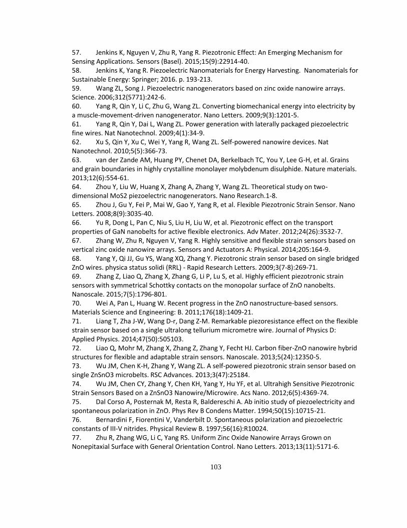
103
57. Jenkins K, Nguyen V, Zhu R, Yang R. Piezotronic Effect: An Emerging Mechanism for Sensing Applications. Sensors (Basel). 2015;15(9):22914-40. 58. Jenkins K, Yang R. Piezoelectric Nanomaterials for Energy Harvesting. Nanomaterials for Sustainable Energy: Springer; 2016. p. 193-213. 59. Wang ZL, Song J. Piezoelectric nanogenerators based on zinc oxide nanowire arrays. Science. 2006;312(5771):242-6. 60. Yang R, Qin Y, Li C, Zhu G, Wang ZL. Converting biomechanical energy into electricity by a muscle-movement-driven nanogenerator. Nano Letters. 2009;9(3):1201-5. 61. Yang R, Qin Y, Dai L, Wang ZL. Power generation with laterally packaged piezoelectric fine wires. Nat Nanotechnol. 2009;4(1):34-9. 62. Xu S, Qin Y, Xu C, Wei Y, Yang R, Wang ZL. Self-powered nanowire devices. Nat Nanotechnol. 2010;5(5):366-73. 63. van der Zande AM, Huang PY, Chenet DA, Berkelbach TC, You Y, Lee G-H, et al. Grains and grain boundaries in highly crystalline monolayer molybdenum disulphide. Nature materials. 2013;12(6):554-61. 64. Zhou Y, Liu W, Huang X, Zhang A, Zhang Y, Wang ZL. Theoretical study on two-dimensional MoS2 piezoelectric nanogenerators. Nano Research.1-8. 65. Zhou J, Gu Y, Fei P, Mai W, Gao Y, Yang R, et al. Flexible Piezotronic Strain Sensor. Nano Letters. 2008;8(9):3035-40. 66. Yu R, Dong L, Pan C, Niu S, Liu H, Liu W, et al. Piezotronic effect on the transport properties of GaN nanobelts for active flexible electronics. Adv Mater. 2012;24(26):3532-7. 67. Zhang W, Zhu R, Nguyen V, Yang R. Highly sensitive and flexible strain sensors based on vertical zinc oxide nanowire arrays. Sensors and Actuators A: Physical. 2014;205:164-9. 68. Yang Y, Qi JJ, Gu YS, Wang XQ, Zhang Y. Piezotronic strain sensor based on single bridged ZnO wires. physica status solidi (RRL) - Rapid Research Letters. 2009;3(7-8):269-71. 69. Zhang Z, Liao Q, Zhang X, Zhang G, Li P, Lu S, et al. Highly efficient piezotronic strain sensors with symmetrical Schottky contacts on the monopolar surface of ZnO nanobelts. Nanoscale. 2015;7(5):1796-801. 70. Wei A, Pan L, Huang W. Recent progress in the ZnO nanostructure-based sensors. Materials Science and Engineering: B. 2011;176(18):1409-21. 71. Liang T, Zha J-W, Wang D-r, Dang Z-M. Remarkable piezoresistance effect on the flexible strain sensor based on a single ultralong tellurium micrometre wire. Journal of Physics D: Applied Physics. 2014;47(50):505103. 72. Liao Q, Mohr M, Zhang X, Zhang Z, Zhang Y, Fecht HJ. Carbon fiber-ZnO nanowire hybrid structures for flexible and adaptable strain sensors. Nanoscale. 2013;5(24):12350-5. 73. Wu JM, Chen K-H, Zhang Y, Wang ZL. A self-powered piezotronic strain sensor based on single ZnSnO3 microbelts. RSC Advances. 2013;3(47):25184. 74. Wu JM, Chen CY, Zhang Y, Chen KH, Yang Y, Hu YF, et al. Ultrahigh Sensitive Piezotronic Strain Sensors Based on a ZnSnO3 Nanowire/Microwire. Acs Nano. 2012;6(5):4369-74. 75. Dal Corso A, Posternak M, Resta R, Baldereschi A. Ab initio study of piezoelectricity and spontaneous polarization in ZnO. Phys Rev B Condens Matter. 1994;50(15):10715-21. 76. Bernardini F, Fiorentini V, Vanderbilt D. Spontaneous polarization and piezoelectric constants of III-V nitrides. Physical Review B. 1997;56(16):R10024. 77. Zhu R, Zhang WG, Li C, Yang RS. Uniform Zinc Oxide Nanowire Arrays Grown on Nonepitaxial Surface with General Orientation Control. Nano Letters. 2013;13(11):5171-6.
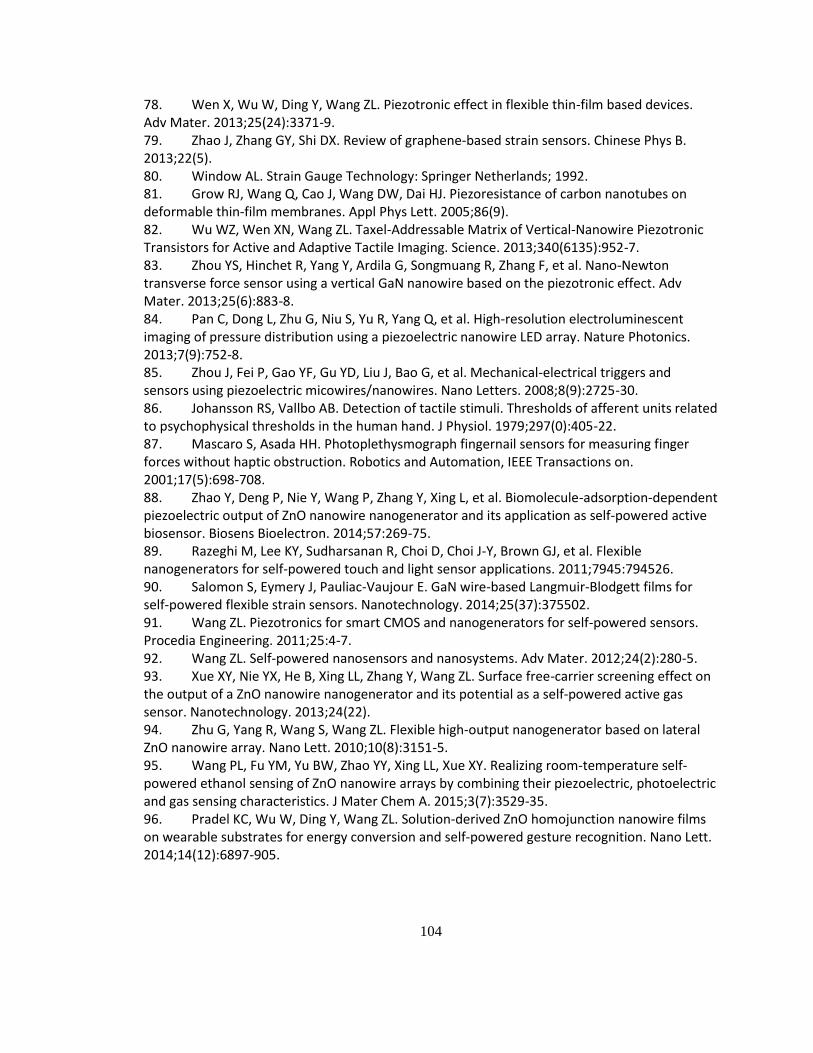
104
78. Wen X, Wu W, Ding Y, Wang ZL. Piezotronic effect in flexible thin-film based devices. Adv Mater. 2013;25(24):3371-9. 79. Zhao J, Zhang GY, Shi DX. Review of graphene-based strain sensors. Chinese Phys B. 2013;22(5). 80. Window AL. Strain Gauge Technology: Springer Netherlands; 1992. 81. Grow RJ, Wang Q, Cao J, Wang DW, Dai HJ. Piezoresistance of carbon nanotubes on deformable thin-film membranes. Appl Phys Lett. 2005;86(9). 82. Wu WZ, Wen XN, Wang ZL. Taxel-Addressable Matrix of Vertical-Nanowire Piezotronic Transistors for Active and Adaptive Tactile Imaging. Science. 2013;340(6135):952-7. 83. Zhou YS, Hinchet R, Yang Y, Ardila G, Songmuang R, Zhang F, et al. Nano-Newton transverse force sensor using a vertical GaN nanowire based on the piezotronic effect. Adv Mater. 2013;25(6):883-8. 84. Pan C, Dong L, Zhu G, Niu S, Yu R, Yang Q, et al. High-resolution electroluminescent imaging of pressure distribution using a piezoelectric nanowire LED array. Nature Photonics. 2013;7(9):752-8. 85. Zhou J, Fei P, Gao YF, Gu YD, Liu J, Bao G, et al. Mechanical-electrical triggers and sensors using piezoelectric micowires/nanowires. Nano Letters. 2008;8(9):2725-30. 86. Johansson RS, Vallbo AB. Detection of tactile stimuli. Thresholds of afferent units related to psychophysical thresholds in the human hand. J Physiol. 1979;297(0):405-22. 87. Mascaro S, Asada HH. Photoplethysmograph fingernail sensors for measuring finger forces without haptic obstruction. Robotics and Automation, IEEE Transactions on. 2001;17(5):698-708. 88. Zhao Y, Deng P, Nie Y, Wang P, Zhang Y, Xing L, et al. Biomolecule-adsorption-dependent piezoelectric output of ZnO nanowire nanogenerator and its application as self-powered active biosensor. Biosens Bioelectron. 2014;57:269-75. 89. Razeghi M, Lee KY, Sudharsanan R, Choi D, Choi J-Y, Brown GJ, et al. Flexible nanogenerators for self-powered touch and light sensor applications. 2011;7945:794526. 90. Salomon S, Eymery J, Pauliac-Vaujour E. GaN wire-based Langmuir-Blodgett films for self-powered flexible strain sensors. Nanotechnology. 2014;25(37):375502. 91. Wang ZL. Piezotronics for smart CMOS and nanogenerators for self-powered sensors. Procedia Engineering. 2011;25:4-7. 92. Wang ZL. Self-powered nanosensors and nanosystems. Adv Mater. 2012;24(2):280-5. 93. Xue XY, Nie YX, He B, Xing LL, Zhang Y, Wang ZL. Surface free-carrier screening effect on the output of a ZnO nanowire nanogenerator and its potential as a self-powered active gas sensor. Nanotechnology. 2013;24(22). 94. Zhu G, Yang R, Wang S, Wang ZL. Flexible high-output nanogenerator based on lateral ZnO nanowire array. Nano Lett. 2010;10(8):3151-5. 95. Wang PL, Fu YM, Yu BW, Zhao YY, Xing LL, Xue XY. Realizing room-temperature self-powered ethanol sensing of ZnO nanowire arrays by combining their piezoelectric, photoelectric and gas sensing characteristics. J Mater Chem A. 2015;3(7):3529-35. 96. Pradel KC, Wu W, Ding Y, Wang ZL. Solution-derived ZnO homojunction nanowire films on wearable substrates for energy conversion and self-powered gesture recognition. Nano Lett. 2014;14(12):6897-905.
105
97. Romano G, Mantini G, Di Carlo A, D'Amico A, Falconi C, Wang ZL. Piezoelectric potential in vertically aligned nanowires for high output nanogenerators. Nanotechnology. 2011;22(46):465401. 98. Lee E, Park J, Yim M, Kim Y, Yoon G. Characteristics of piezoelectric ZnO/AlN−stacked flexible nanogenerators for energy harvesting applications. Appl Phys Lett. 2015;106(2):023901. 99. Pi Z, Zhang J, Wen C, Zhang Z-b, Wu D. Flexible piezoelectric nanogenerator made of poly (vinylidenefluoride-co-trifluoroethylene)(PVDF-TrFE) thin film. Nano Energy. 2014;7:33-41. 100. Huang X, Li L, Zhang Y. Modeling the open circuit output voltage of piezoelectric nanogenerator. Science China Technological Sciences. 2013;56(11):2622-9. 101. Schubert MA, Senz S, Alexe M, Hesse D, Gösele U. Finite element method calculations of ZnO nanowires for nanogenerators. Appl Phys Lett. 2008;92(12):122904. 102. Tao R, Hinchet R, Ardila G, Montès L, Mouis M, editors. FEM modeling of vertically integrated nanogenerators in compression and flexion modes. Ph D Research in Microelectronics and Electronics (PRIME), 2014 10th Conference on; 2014: IEEE. 103. Wang ZL. Piezotronics and Piezo‐Phototronics: Wiley Online Library; 2012. 104. Comsol Multiphysics, Version 5.0. 105. Bdikin I, Bystrov V, Kopyl S, Lopes RPG, Delgadillo I, Gracio J, et al. Evidence of ferroelectricity and phase transition in pressed diphenylalanine peptide nanotubes. Appl Phys Lett. 2012;100(4):043702. 106. Qiu Y, Zhang H, Hu L, Yang D, Wang L, Wang B, et al. Flexible piezoelectric nanogenerators based on ZnO nanorods grown on common paper substrates. Nanoscale. 2012;4(20):6568-73. 107. Kim SK, Bhatia R, Kim T-H, Seol D, Kim JH, Kim H, et al. Directional dependent piezoelectric effect in CVD grown monolayer MoS2 for flexible piezoelectric nanogenerators. Nano Energy. 2016;22:483-9. 108. Chang C, Tran VH, Wang J, Fuh Y-K, Lin L. Direct-write piezoelectric polymeric nanogenerator with high energy conversion efficiency. Nano letters. 2010;10(2):726-31. 109. Lee BY, Zhang J, Zueger C, Chung WJ, Yoo SY, Wang E, et al. Virus-based piezoelectric energy generation. Nat Nanotechnol. 2012;7(6):351-6. 110. Ziegler-Graham K, MacKenzie EJ, Ephraim PL, Travison TG, Brookmeyer R. Estimating the prevalence of limb loss in the United States: 2005 to 2050. Arch Phys Med Rehabil. 2008;89(3):422-9. 111. Tan DW, Schiefer MA, Keith MW, Anderson JR, Tyler J, Tyler DJ. A neural interface provides long-term stable natural touch perception. Sci Transl Med. 2014;6(257):257ra138. 112. Raspopovic S, Capogrosso M, Petrini FM, Bonizzato M, Rigosa J, Di Pino G, et al. Restoring natural sensory feedback in real-time bidirectional hand prostheses. Sci Transl Med. 2014;6(222):222ra19. 113. Hammock ML, Chortos A, Tee BC, Tok JB, Bao Z. 25th anniversary article: The evolution of electronic skin (e-skin): a brief history, design considerations, and recent progress. Adv Mater. 2013;25(42):5997-6038. 114. Antfolk C, D'Alonzo M, Controzzi M, Lundborg G, Rosen B, Sebelius F, et al. Artificial redirection of sensation from prosthetic fingers to the phantom hand map on transradial amputees: vibrotactile versus mechanotactile sensory feedback. IEEE Trans Neural Syst Rehabil Eng. 2013;21(1):112-20.
106
115. Cipriani C, D'Alonzo M, Carrozza MC. A miniature vibrotactile sensory substitution device for multifingered hand prosthetics. IEEE Trans Biomed Eng. 2012;59(2):400-8. 116. Shill JJ, Collins EG, Jr., Coyle E, Clark J. Tactile surface classification for limbed robots using a pressure sensitive robot skin. Bioinspir Biomim. 2015;10(1):016012. 117. D'Alonzo M, Dosen S, Cipriani C, Farina D. HyVE: hybrid vibro-electrotactile stimulation for sensory feedback and substitution in rehabilitation. IEEE Trans Neural Syst Rehabil Eng. 2014;22(2):290-301. 118. Francomano MT, Accoto D, Guglielmelli E. Artificial sense of slip—A review. IEEE Sensors Journal. 2013;13(7):2489-98. 119. Dahiya RS, Metta G, Valle M, Sandini G. Tactile Sensing—From Humans to Humanoids. IEEE Transactions on Robotics. 2010;26(1):1-20. 120. McGlone F, Reilly D. The cutaneous sensory system. Neuroscience & Biobehavioral Reviews. 2010;34(2):148-59. 121. Bear MF, Connors BW, Paradiso MA. Neuroscience: Lippincott Williams & Wilkins; 2007. 122. Johansson R, Vallbo Å, Westling G. Thresholds of mechanosensitive afferents in the human hand as measured with von Frey hairs. Brain research. 1980;184(2):343-51. 123. Skedung L, Arvidsson M, Chung JY, Stafford CM, Berglund B, Rutland MW. Feeling small: exploring the tactile perception limits. Scientific reports. 2013;3:2617. 124. Lucarotti C, Oddo CM, Vitiello N, Carrozza MC. Synthetic and bio-artificial tactile sensing: a review. Sensors (Basel). 2013;13(2):1435-66. 125. Cheng MY, Huang XH, Ma CW, Yang YJ. A flexible capacitive tactile sensing array with floating electrodes. Journal of Micromechanics and Microengineering. 2009;19(11):115001. 126. Ponce Wong RD, Posner JD, Santos VJ. Flexible microfluidic normal force sensor skin for tactile feedback. Sensors and Actuators A: Physical. 2012;179:62-9. 127. Hyung-Kew L, Jaehoon C, Sun-Il C, Euisik Y. Normal and Shear Force Measurement Using a Flexible Polymer Tactile Sensor With Embedded Multiple Capacitors. Journal of Microelectromechanical Systems. 2008;17(4):934-42. 128. Hu Y, Katragadda RB, Tu H, Zheng Q, Li Y, Xu Y. Bioinspired 3-D Tactile Sensor for Minimally Invasive Surgery. Journal of Microelectromechanical Systems. 2010;19(6):1400-8. 129. Chuang C-H, Dong W-B, Lo W-B, editors. Flexible piezoelectric tactile sensor with structural electrodes array for shape recognition system. Sensing Technology, 2008 ICST 2008 3rd International Conference on; 2008: IEEE. 130. Muhammad H, Hunt N, Shelton R, Grover L, Ward M, Oddo C, et al., editors. Incorporation of novel MEMS tactile sensors into tissue engineered skin. Bioinformatics and Biomedical Engineering (iCBBE), 2010 4th International Conference on; 2010: IEEE. 131. Cheneler D, Ward MCL, Anthony CJ. Bio-hybrid tactile sensor for the study of the role of mechanoreceptors in human tactile perception. Microelectronic Engineering. 2012;97:297-300. 132. Merzenich MM, Nelson RJ, Stryker MP, Cynader MS, Schoppmann A, Zook JM. Somatosensory cortical map changes following digit amputation in adult monkeys. Journal of comparative Neurology. 1984;224(4):591-605. 133. Mercier C, Reilly KT, Vargas CD, Aballea A, Sirigu A. Mapping phantom movement representations in the motor cortex of amputees. Brain. 2006;129(8):2202-10. 134. Reilly KT, Mercier C, Schieber MH, Sirigu A. Persistent hand motor commands in the amputees' brain. Brain. 2006;129(8):2211-23.
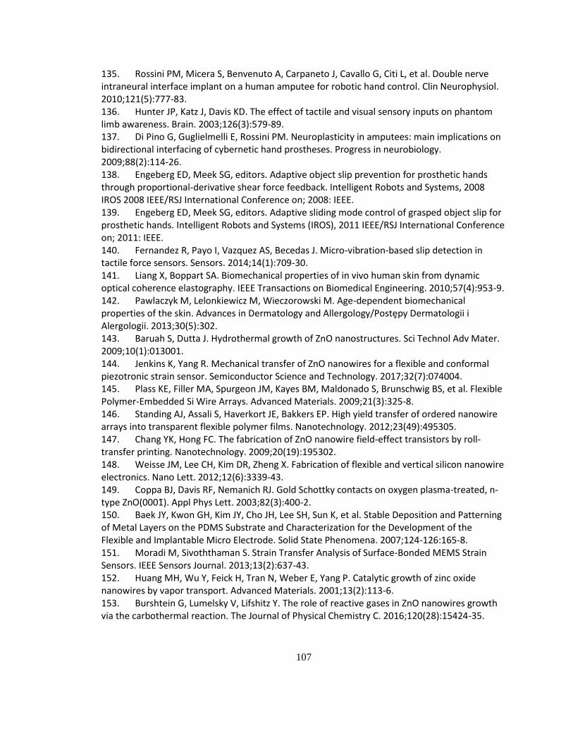
107
135. Rossini PM, Micera S, Benvenuto A, Carpaneto J, Cavallo G, Citi L, et al. Double nerve intraneural interface implant on a human amputee for robotic hand control. Clin Neurophysiol. 2010;121(5):777-83. 136. Hunter JP, Katz J, Davis KD. The effect of tactile and visual sensory inputs on phantom limb awareness. Brain. 2003;126(3):579-89. 137. Di Pino G, Guglielmelli E, Rossini PM. Neuroplasticity in amputees: main implications on bidirectional interfacing of cybernetic hand prostheses. Progress in neurobiology. 2009;88(2):114-26. 138. Engeberg ED, Meek SG, editors. Adaptive object slip prevention for prosthetic hands through proportional-derivative shear force feedback. Intelligent Robots and Systems, 2008 IROS 2008 IEEE/RSJ International Conference on; 2008: IEEE. 139. Engeberg ED, Meek SG, editors. Adaptive sliding mode control of grasped object slip for prosthetic hands. Intelligent Robots and Systems (IROS), 2011 IEEE/RSJ International Conference on; 2011: IEEE. 140. Fernandez R, Payo I, Vazquez AS, Becedas J. Micro-vibration-based slip detection in tactile force sensors. Sensors. 2014;14(1):709-30. 141. Liang X, Boppart SA. Biomechanical properties of in vivo human skin from dynamic optical coherence elastography. IEEE Transactions on Biomedical Engineering. 2010;57(4):953-9. 142. Pawlaczyk M, Lelonkiewicz M, Wieczorowski M. Age-dependent biomechanical properties of the skin. Advances in Dermatology and Allergology/Postȩpy Dermatologii i Alergologii. 2013;30(5):302. 143. Baruah S, Dutta J. Hydrothermal growth of ZnO nanostructures. Sci Technol Adv Mater. 2009;10(1):013001. 144. Jenkins K, Yang R. Mechanical transfer of ZnO nanowires for a flexible and conformal piezotronic strain sensor. Semiconductor Science and Technology. 2017;32(7):074004. 145. Plass KE, Filler MA, Spurgeon JM, Kayes BM, Maldonado S, Brunschwig BS, et al. Flexible Polymer-Embedded Si Wire Arrays. Advanced Materials. 2009;21(3):325-8. 146. Standing AJ, Assali S, Haverkort JE, Bakkers EP. High yield transfer of ordered nanowire arrays into transparent flexible polymer films. Nanotechnology. 2012;23(49):495305. 147. Chang YK, Hong FC. The fabrication of ZnO nanowire field-effect transistors by roll-transfer printing. Nanotechnology. 2009;20(19):195302. 148. Weisse JM, Lee CH, Kim DR, Zheng X. Fabrication of flexible and vertical silicon nanowire electronics. Nano Lett. 2012;12(6):3339-43. 149. Coppa BJ, Davis RF, Nemanich RJ. Gold Schottky contacts on oxygen plasma‐treated, n‐type ZnO(0001). Appl Phys Lett. 2003;82(3):400-2. 150. Baek JY, Kwon GH, Kim JY, Cho JH, Lee SH, Sun K, et al. Stable Deposition and Patterning of Metal Layers on the PDMS Substrate and Characterization for the Development of the Flexible and Implantable Micro Electrode. Solid State Phenomena. 2007;124-126:165-8. 151. Moradi M, Sivoththaman S. Strain Transfer Analysis of Surface-Bonded MEMS Strain Sensors. IEEE Sensors Journal. 2013;13(2):637-43. 152. Huang MH, Wu Y, Feick H, Tran N, Weber E, Yang P. Catalytic growth of zinc oxide nanowires by vapor transport. Advanced Materials. 2001;13(2):113-6. 153. Burshtein G, Lumelsky V, Lifshitz Y. The role of reactive gases in ZnO nanowires growth via the carbothermal reaction. The Journal of Physical Chemistry C. 2016;120(28):15424-35.
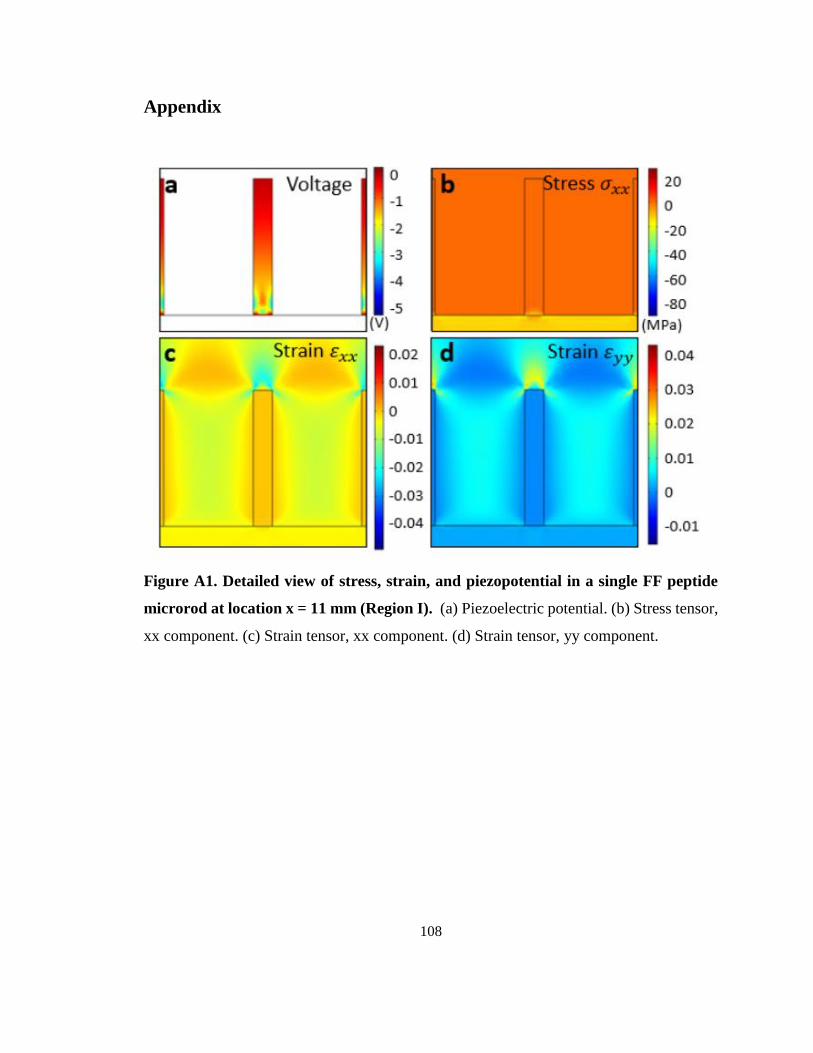
108
Appendix
Figure A1. Detailed view of stress, strain, and piezopotential in a single FF peptide
microrod at location x = 11 mm (Region I). (a) Piezoelectric potential. (b) Stress tensor,
xx component. (c) Strain tensor, xx component. (d) Strain tensor, yy component.
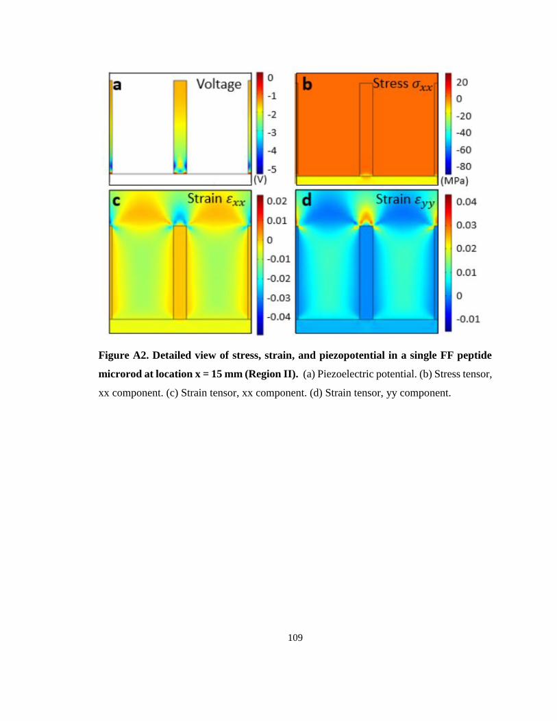
109
Figure A2. Detailed view of stress, strain, and piezopotential in a single FF peptide
microrod at location x = 15 mm (Region II). (a) Piezoelectric potential. (b) Stress tensor,
xx component. (c) Strain tensor, xx component. (d) Strain tensor, yy component.
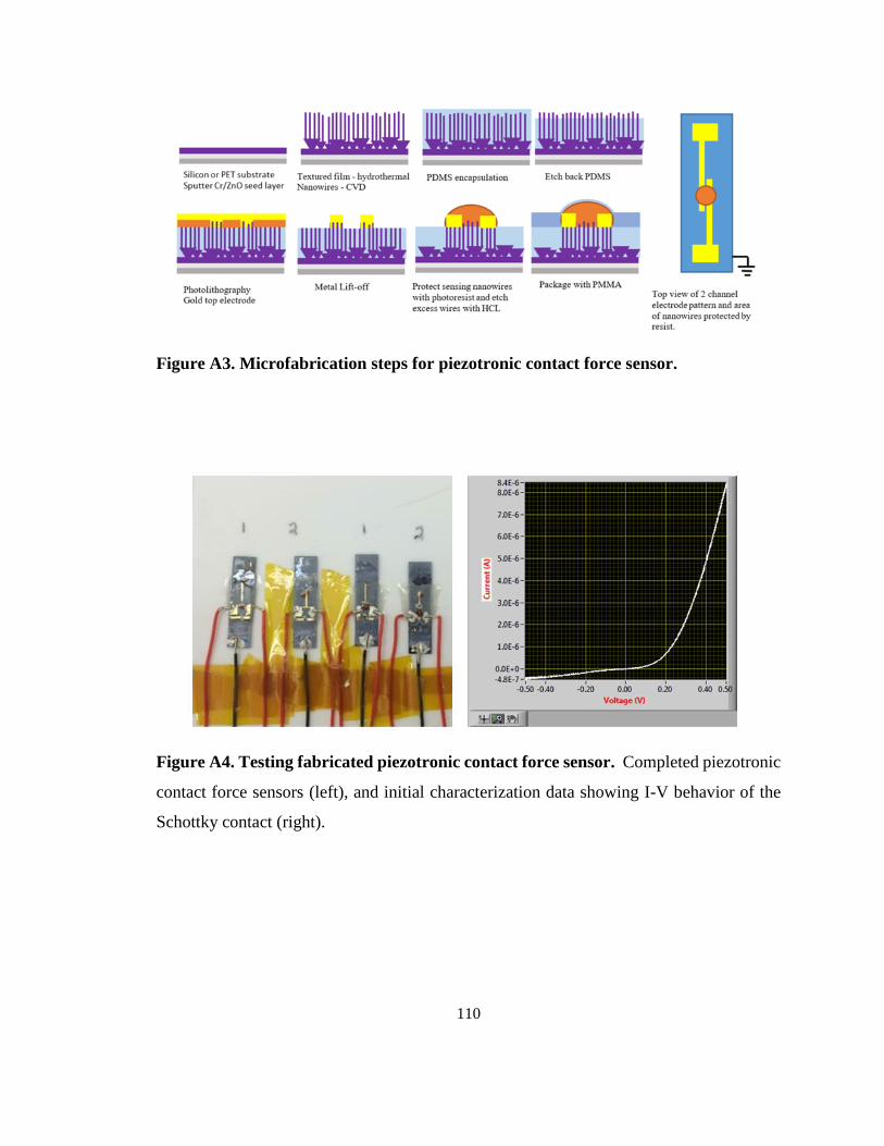
110
Figure A3. Microfabrication steps for piezotronic contact force sensor.
Figure A4. Testing fabricated piezotronic contact force sensor. Completed piezotronic
contact force sensors (left), and initial characterization data showing I-V behavior of the
Schottky contact (right).


