Embed Size (px)
Citation preview

IOP PUBLISHING JOURNAL OF MICROMECHANICS AND MICROENGINEERING
J. Micromech. Microeng. 18 (2008) 015023 (10pp) doi:10.1088/0960-1317/18/1/015023
A piezoelectric microvalve for cryogenicapplicationsJong M Park1, Ryan P Taylor2, Allan T Evans1, Tyler R Brosten2,Gregory F Nellis2, Sanford A Klein2, Jeffrey R Feller3, Louis Salerno3
and Yogesh B Gianchandani1
1 Department of Electrical Engineering and Computer Science, University of Michigan, Ann Arbor,1301 Beal Ave., Ann Arbor, MI 48109, USA2 Department of Mechanical Engineering, University of Wisconsin, Madison, 1500 Engineering Dr.,Madison, WI 53706, USA3 NASA Ames Research Center, Moffett Field, CA 94035, USA
E-mail: [email protected]
Received 23 August 2007, in final form 9 November 2007Published 11 December 2007Online at stacks.iop.org/JMM/18/015023
AbstractThis paper reports on a normally open piezoelectrically actuated microvalve for high flowmodulation at cryogenic temperatures. One application envisioned is to control the flow of acryogen for distributed cooling with a high degree of temperature stability and a small thermalgradient. The valve consists of a micromachined die fabricated from a silicon-on-insulatorwafer, a glass wafer, a commercially available piezoelectric stack actuator and MacorTM
ceramic encapsulation that has overall dimensions of 1 × 1 × 1 cm3. A perimeteraugmentation scheme for the valve seat has been implemented to provide high flowmodulation. In tests performed at room temperature the flow was modulated from980 mL min−1 with the valve fully open (0 V), to 0 mL min−1 with a 60 V actuation voltage, atan inlet gauge pressure of 55 kPa. This range is orders of magnitude higher flow than themodulation capability of similarly sized piezoelectric microvalves. At the cryogenictemperature of 80 K, the valve successfully modulated gas flow from 350 mL min−1 down to20 mL min−1 with an inlet pressure of 104 kPa higher than the atmosphere. The operation ofthis valve has been validated at elevated temperatures as well, up to 380 K. The valve has aresponse time of less than 1 ms and has operational bandwidth up to 820 kHz.
(Some figures in this article are in colour only in the electronic version)
1. Introduction
Future space missions will require cooling of large opticalstructures and cryogenic storage systems with a high degreeof temperature stability and a small temperature gradient[1, 2]. It is challenging to provide strict thermal stabilityto these large structures with a single cryocooler. Anattractive solution is to implement a distributed network ofelements that provide appropriate cooling for the system.More specifically, multiple cooling elements, each consistingof actively controlled valves, integrated heat exchangersand temperature sensors, will be positioned across thestructure to be cooled. The actively controlled valves arecapable of regulating the flow of refrigerant in response
to local temperature. With each cooling element workingindependently in response to local sensors, temperature can becontrolled efficiently. In order to realize such a distributedcooling system, it is essential to have valves that workreliably at cryogenic temperatures and can provide a largeflow modulation capability. Due to the intended operation in aspace environment as a part of the cryogenic cooling system,the active microvalve must have a wide range of operatingtemperature, remaining functional at cryogenic temperaturesduring operation and at ambient and even slightly elevatedtemperature for qualification testing and contamination controlprocesses. The valve must provide a high degree of flowmodulation for adequate cooling. Since excess cooling istolerable, a normally open valve is desirable; the open state
0960-1317/08/015023+10$30.00 1 © 2008 IOP Publishing Ltd Printed in the UK
J. Micromech. Microeng. 18 (2008) 015023 J M Park et al
is a safe failure mode that does not block refrigerant flow.Finally, for some applications it is desirable that the valve beable to withstand a large pressure difference so that it canaccomplish the free expansion in a Joule–Thompson coolingcycle.
Several actuation schemes were considered to meetthese demands. One of the first active micromachinedvalves reported in the literature, which uses electromagneticactuation, consists of an etched silicon orifice, a nickeldiaphragm, and a solenoid actuator and plunger assembly [3].The main advantage of magnetic actuation is the ability tocreate a relatively large force and large deflections with alow driving voltage. However, magnetic actuation tends torequire significant power for operation, up to several watts[4–6]. Electrostatic actuation is characterized by a fastresponse and low power consumption; however, the force isrelatively small, limiting its applications to low inlet pressures.Furthermore, arrays of valves are needed for flow control,because electrostatically driven valves are typically operatedin a binary mode rather than as proportional valves [7–9].A pressure-balancing scheme has been explored for highpressure applications, but abrupt turn-on behavior is inevitable[10]. Various forms of thermal actuation schemes suchas thermopneumatic [11, 12], bimetallic [13–15] and shapememory alloy [16] take advantage of thermal properties ofmaterials to generate displacements. These actuation schemesgenerally produce considerable force while simultaneouslyachieving relatively large displacements. However, these haverelatively high power consumption and slow response times.In addition, their performance may be degraded when operatedat cryogenic temperatures.
For this work, piezoelectric actuation was chosen becauseit allows proportional flow control and is capable of generatinghigh force with low power consumption. Out-of-plane,stacked PZT (lead zirconate titanate) actuation has been widelyused in valves. One of the earliest works on fabricationof a piezoelectric microvalve was presented by Esashi et al[17–19]. The valve is constructed from silicon mesa suspendedwith a flexible silicon diaphragm pressed against a glass plateor a polymer membrane by a stack piezoelectric actuator.While piezoelectric microvalves have been developed forspace applications [20, 21], these were not designed forcryogenic operation and for high flow modulation. A majordisadvantage of piezoelectric actuation is its small stroke,even for large voltages. At cryogenic temperatures, thedisplacement is further reduced due to degradation of thepiezoelectric coefficient. This drawback can be potentiallyovercome by hydraulic amplification; however, fabrication ofsuch devices is often complicated [22, 23]. In this effort, theflow limitation imposed by the small displacement is addressedby perimeter augmentation of the valve seat. A ceramiccasing is utilized to reduce the thermal mismatch between thepackaging material and the PZT actuator, and the actuator ispre-stressed during assembly to provide a normally open valve.The development, modeling and test results of piezoelectricvalves fabricated from Si, glass and ceramic are presented.The valves are evaluated at low temperature, as well as in ahigh pressure environment4.4 Portions of this work were published in conference abstract form in [24].
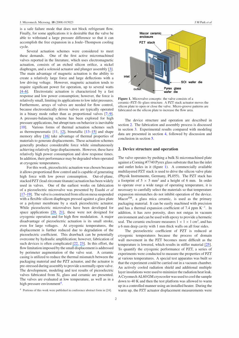
Figure 1. Microvalve concepts: the valve consists of aceramic–PZT–Si–glass structure. A PZT stack actuator moves thesilicon plate to open or close the valve. Micro-groove patterns arefabricated on the silicon plate to increase the flow area.
The device structure and operation are described insection 2. The fabrication and assembly process is discussedin section 3. Experimental results compared with modelingdata are presented in section 4, followed by discussion andconclusion in section 5.
2. Device structure and operation
The valve operates by pushing a bulk Si micromachined plateagainst a Corning #7740 Pyrex glass substrate that has the inletand outlet holes in it (figure 1). A commercially availablemultilayered PZT stack is used to drive the silicon valve plate(Physik Instrumente, Germany, PL055). The PZT stack hasa footprint of 5 × 5 mm2 and a height of 6 mm. In orderto operate over a wide range of operating temperature, it isnecessary to carefully select the materials so that temperatureexpansion mismatches do not inhibit operation of the device.MacorTM, a glass mica ceramic, is used as the primarypackaging material. It can be easily machined with precisionand has a thermal expansion coefficient of 7.4 ppm K−1. Inaddition, it has zero porosity, does not outgas in vacuumenvironment and can be used with epoxy to provide a hermeticseal. The ceramic enclosure measures 1 × 1 × 1 cm3, and hasa 6 mm deep cavity with 1 mm thick walls on all four sides.
The piezoelectric coefficient of PZT is reduced atcryogenic temperatures because the process of domainwall movement in the PZT becomes more difficult as thetemperature is lowered, which results in stiffer material [25].To quantify the cryogenic performance of PZT, a series ofexperiments were conducted to measure the properties of PZTat various temperatures. A special test apparatus was built sothat the experiment could be carried out in a vacuum chamber.An actively cooled radiation shield and additional multiplelayer insulations were used to minimize the radiation heat leak.A Cryomech AL60 GM cryocooler was used to cool the sampledown to 40 K and then the test platform was allowed to warmup in a controlled manner using an installed heater. During thewarm up, the PZT actuator displacement measurements were
2

J. Micromech. Microeng. 18 (2008) 015023 J M Park et al
Figure 2. Measured PZT stack actuation constant (strain per unitvoltage) as a function of temperature. The data are separated intotwo categories related to the increasing and decreasing voltages. Asthe operating temperature is reduced, the actuator constantdecreases.
taken at various temperatures using two fiber-optic probes.More details about the experiments can be found in [26]. Forconvenience, an actuator constant for this particular PZT isdefined as strain per unit voltage, and this actuator constantat various temperatures is presented in figure 2. Note that theactuator displacement gradually reduces as the temperaturedecreases; at 40 K, it is approximately one third of the roomtemperature value.
The degraded performance of PZT at cryogenictemperatures poses another design challenge for thismicrovalve in providing sufficient flow rate. The followingsimple calculation provides an estimate of the flow that isrequired to provide adequate cooling. Assume that a potentialapplication requires that 1.0 W of cooling load (q) be acceptedby a flow of helium that is at a nominal pressure (Pnom) of1.0 MPa and temperature (Tnom) of 25 K. The temperature rise(�T) specifies the mass flow rate that is required (m) accordingto an energy balance:
q = mcp�T (1)
where cp is the nominal constant pressure specific heatcapacity. For a 1.0 W load with a 0.1 K temperature rise,the required mass flow rate is 1.8 g s−1. The pressure drop(�P ) coupled with the mass flow rate specifies the nominalvalve flow area (Avalve) which is illustrated in equation (2).
�P = CDm2
2ρA2valve
(2)
where ρ is the nominal density and CD is a nominal dischargecoefficient that is close to unity [27]. If the pressure drop isassumed to be kept at 10 kPa to avoid excessively burdeningthe fluid circulation system then equation (2) illustrates thata valve flow area of 3.0 × 10⁻⁶ m2 is required. In this case,the flow area is given by the product of valve seat perimetersurrounding inlet or outlet hole (p) and the separation betweenthe silicon valve plate and glass seat (δ).
Avalve = δ · p. (3)
The required flow area is quite large considering that thePZT actuator can provide at most 6 µm displacement atroom temperature, and even less at lower temperatures. Toachieve this large flow area, the perimeter of the valve seatis substantially increased by implementing serpentine groovepatterns on the silicon valve plate (5 × 5 mm2), as shownschematically in figures 1 and 3. Each groove is 50 µm wideand 120 µm deep and the perimeter measures about 127 mm,capable of providing much larger flow.
The silicon valve plate is suspended by four flexures incrab-leg formation; each measures 500 µm wide, 4200 µmlong and 50 µm thick. These flexures are flexible enoughto move freely upon the actuation of PZT (spring constant≈500 N m−1) but are rigid enough to hold the plate inplace. In addition, the crab-leg formation can relieve anystress that is caused by the large temperature variation. Thischaracteristic was verified by finite element analysis of thestructure. Assuming that the anodic bonding between thesilicon and glass was done at 400 ◦C, at room temperature,the maximum stress of 21 MPa was observed at the cornersof bonding rim but the stress on the flexure and silicon valveplate was negligible.
The bonded die, PZT actuator and ceramic enclosuresare joined using Stycast epoxy, which provides exceptionalstability in cryogenic conditions. The PZT actuator is notbonded to the Si plate, which helps to accommodate variationsin height caused by the expansion mismatch between the PZTand the Macor.
3. Device fabrication
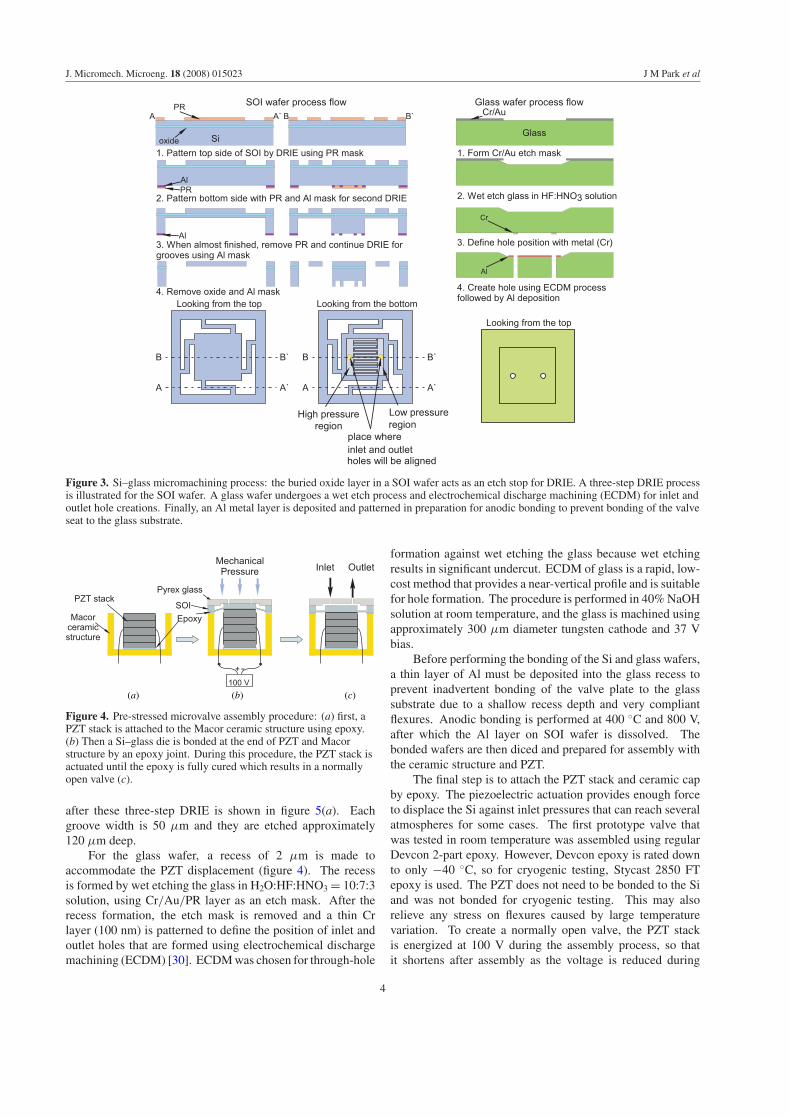
To ensure control of material properties, the final deviceconsists of only bulk materials. Deposited thin films arenot used for any structural layer, although they are used inintermediate steps. The fabrication process uses two wafers:a silicon-on-insulator (SOI) wafer which has a device layer,buried oxide layer and carrier wafer thicknesses of 50 µm,0.5 µm and 450 µm, respectively, and a 500 µm thick Pyrexglass wafer. The fabrication processes for SOI and glass wafersare illustrated in figure 3, and the assembly with the PZT andthe ceramic housing is illustrated in figure 4.
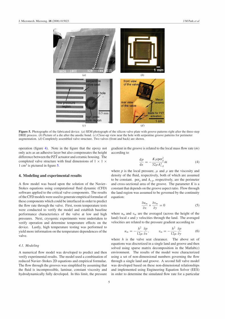
Deep reactive ion etching (DRIE) of silicon was usedto form flexures, the valve plate and groove patterns in theplate. DRIE provides high etching speed, high aspect ratiocapabilities and good selectivity. However, the uniformity ofDRIE is not reliable across a full wafer [28, 29]. The buriedoxide layer in SOI wafers provides an etch stop for DRIE,while the epitaxial layer provides a well-controlled flexurethickness, smooth surfaces and bulk Si properties. The firstDRIE step etches down to the buried oxide layer from thetop and defines the flexure structures. Then the bottom sideis patterned with Al and photoresist. The photoresist acts asan etch mask for the second DRIE step that is approximately400 µm deep. Next, the photoresist is removed and Al isused as an etch mask for the final DRIE step which engravesserpentine grooves for perimeter augmentation. The Al layeris then removed and the wafer is prepared for bonding. Ascanning electron microscope (SEM) image of a valve plate
3
J. Micromech. Microeng. 18 (2008) 015023 J M Park et al
Figure 3. Si–glass micromachining process: the buried oxide layer in a SOI wafer acts as an etch stop for DRIE. A three-step DRIE processis illustrated for the SOI wafer. A glass wafer undergoes a wet etch process and electrochemical discharge machining (ECDM) for inlet andoutlet hole creations. Finally, an Al metal layer is deposited and patterned in preparation for anodic bonding to prevent bonding of the valveseat to the glass substrate.
(b)(a) (c)
Figure 4. Pre-stressed microvalve assembly procedure: (a) first, aPZT stack is attached to the Macor ceramic structure using epoxy.(b) Then a Si–glass die is bonded at the end of PZT and Macorstructure by an epoxy joint. During this procedure, the PZT stack isactuated until the epoxy is fully cured which results in a normallyopen valve (c).
after these three-step DRIE is shown in figure 5(a). Eachgroove width is 50 µm and they are etched approximately120 µm deep.
For the glass wafer, a recess of 2 µm is made toaccommodate the PZT displacement (figure 4). The recessis formed by wet etching the glass in H2O:HF:HNO3 = 10:7:3solution, using Cr/Au/PR layer as an etch mask. After therecess formation, the etch mask is removed and a thin Crlayer (100 nm) is patterned to define the position of inlet andoutlet holes that are formed using electrochemical dischargemachining (ECDM) [30]. ECDM was chosen for through-hole
formation against wet etching the glass because wet etchingresults in significant undercut. ECDM of glass is a rapid, low-cost method that provides a near-vertical profile and is suitablefor hole formation. The procedure is performed in 40% NaOHsolution at room temperature, and the glass is machined usingapproximately 300 µm diameter tungsten cathode and 37 Vbias.
Before performing the bonding of the Si and glass wafers,a thin layer of Al must be deposited into the glass recess toprevent inadvertent bonding of the valve plate to the glasssubstrate due to a shallow recess depth and very compliantflexures. Anodic bonding is performed at 400 ◦C and 800 V,after which the Al layer on SOI wafer is dissolved. Thebonded wafers are then diced and prepared for assembly withthe ceramic structure and PZT.
The final step is to attach the PZT stack and ceramic capby epoxy. The piezoelectric actuation provides enough forceto displace the Si against inlet pressures that can reach severalatmospheres for some cases. The first prototype valve thatwas tested in room temperature was assembled using regularDevcon 2-part epoxy. However, Devcon epoxy is rated downto only −40 ◦C, so for cryogenic testing, Stycast 2850 FTepoxy is used. The PZT does not need to be bonded to the Siand was not bonded for cryogenic testing. This may alsorelieve any stress on flexures caused by large temperaturevariation. To create a normally open valve, the PZT stackis energized at 100 V during the assembly process, so thatit shortens after assembly as the voltage is reduced during
4
J. Micromech. Microeng. 18 (2008) 015023 J M Park et al
(a) (b)
0.5 mm
(c) (d )
Figure 5. Photographs of the fabricated device. (a) SEM photograph of the silicon valve plate with groove patterns right after the three-stepDRIE process. (b) Picture of a die after the anodic bond. (c) Close-up view near the hole with serpentine groove patterns for perimeteraugmentation. (d) Completely assembled valve structure. Two valves (front and back) are shown.
operation (figure 4). Note in the figure that the epoxy notonly acts as an adhesive layer but also compensates the heightdifference between the PZT actuator and ceramic housing. Thecompleted valve structure with final dimensions of 1 × 1 ×1 cm3 is pictured in figure 5.
4. Modeling and experimental results
A flow model was based upon the solution of the Navier–Stokes equations using computational fluid dynamic (CFD)software applied to the critical valve components. The resultsof the CFD models were used to generate empirical formulae ofthese components which could be interfaced in order to predictthe flow rate through the valve. First, room temperature testswere conducted to verify the model and establish baselineperformance characteristics of the valve at low and highpressures. Next, cryogenic experiments were undertaken toverify operation and determine temperature effects on thedevice. Lastly, high temperature testing was performed toyield more information on the temperature dependences of thevalve.
4.1. Modeling
A numerical flow model was developed to predict and thenverify experimental results. The model used a combination ofreduced Navier–Stokes 2D equations and empirical formulae.The flow through the grooves was simplified by assuming thatthe fluid is incompressible, laminar, constant viscosity andhydrodynamically fully developed. In this limit, the pressure
gradient in the groove is related to the local mass flow rate (m)according to
dp
dx= −Kµper2
g
32ρA3c,g
m (4)
where p is the local pressure, µ and ρ are the viscosity anddensity of the fluid, respectively, both of which are assumedto be constant. perg and Ac,g, respectively, are the perimeterand cross-sectional area of the groove. The parameter K is aconstant that depends on the groove aspect ratio. Flow throughthe land region was assumed to be governed by the continuityequation:
∂um
∂x+
∂vm
∂y= 0 (5)
where um and vm are the averaged (across the height of theland) local x and y velocities through the land. The averagedvelocities are related to the pressure gradient according to
um = − h2
12µ
∂p
∂x, vm = − h2
12µ
∂p
∂y(6)
where h is the valve seat clearance. The above set ofequations was discretized in a single land and groove and thensolved using sparse matrix decomposition in the Matlab(c)environment. The results of the model were characterizedusing a set of non-dimensional numbers governing the flowthrough a single land and groove. A second full valve modelwas developed based on these non-dimensional relationshipsand implemented using Engineering Equation Solver (EES)in order to determine the simulated flow rate for a particular
5
J. Micromech. Microeng. 18 (2008) 015023 J M Park et al
Figure 6. Schematic of the test setup for the He gas flowmeasurement. Flow rate through the valve is measured whilemonitoring the inlet and outlet pressures. For low or hightemperature testing, heat exchangers are placed to cool or heat theHe gas that enters the valve and also bring it back to roomtemperature as it exits the valve.
valve geometry [31]. More details about the development ofthe numerical flow model can be found in [32].
The model was obtained by assuming that the holediameters for inlet and outlet are 350 µm and displacementof PZT at 60 V is 4 µm. In addition, a linear relationshipbetween PZT displacement and voltage was assumed. Thus,seat clearance from the glass substrate can be expressed as inequation (7):
clearance (µm) = 4 − voltage (V) × 0.067. (7)
4.2. Experimental results
Initial tests were performed at room temperature with Hegas flow. Figure 6 is a schematic of the test. An in-linethermoplastic filter is placed upstream of the device to trapany particles or moisture. Pressure gauges are mounted sothat inlet and outlet pressures can be monitored. A copperpiping (6.35 mm diameter) is connected to 0.4 mm holes inglass through an aluminum header. A ball valve is added at theend so that the outlet pressure can be controlled if necessary.
In the first set of tests, the inlet pressure was regulated(21–55 kPa, gage), and the outlet was maintained atatmosphere, while the flow rate was measured over 0–60 Vactuation. As shown in figure 7, as actuation voltage increases,the PZT expands, the clearance between the silicon valve seatand glass substrate decreases, and thus, flow rate decreases.With the gauge pressure of 55 kPa at the inlet, flow rate couldbe modulated from 0 to 980 mL min−1. At 60 V, the valveleakage was below the measurement limit (<0.1 mL min−1).
In a separate experiment, the valve was tested at a higherinlet pressure of 345 kPa gauge pressure to verify its operationat high pressure, but the pressure difference between the inletand outlet was kept at 34.5 kPa since that is the anticipatedoperating condition for the valve. The test setup for this setof experiments is schematically shown in figure 8. A pressurevessel was used to obtain a high absolute pressure whilemaintaining a relatively low pressure differential across thevalve at room temperature. Absolute pressure was measuredat the inlet of the valve while the pressure difference acrossthe valve and volumetric flow rates was measured. Multiple
(a)
(b)
Figure 7. Flow rates as a function of voltage at room temperaturefrom experimental results (a) and analytic model (b). As theactuation voltage increases, the valve is closed and results in adecreased flow rate.
Figure 8. Schematic of the test setup for the high-pressure,room-temperature gas flow measurement. A pressure vessel wasused to obtain high pressure while maintaining a relatively lowpressure differential across the valve. Throttling valves are used tomaintain precise regulation of the pressure differential between theinlet and outlet.
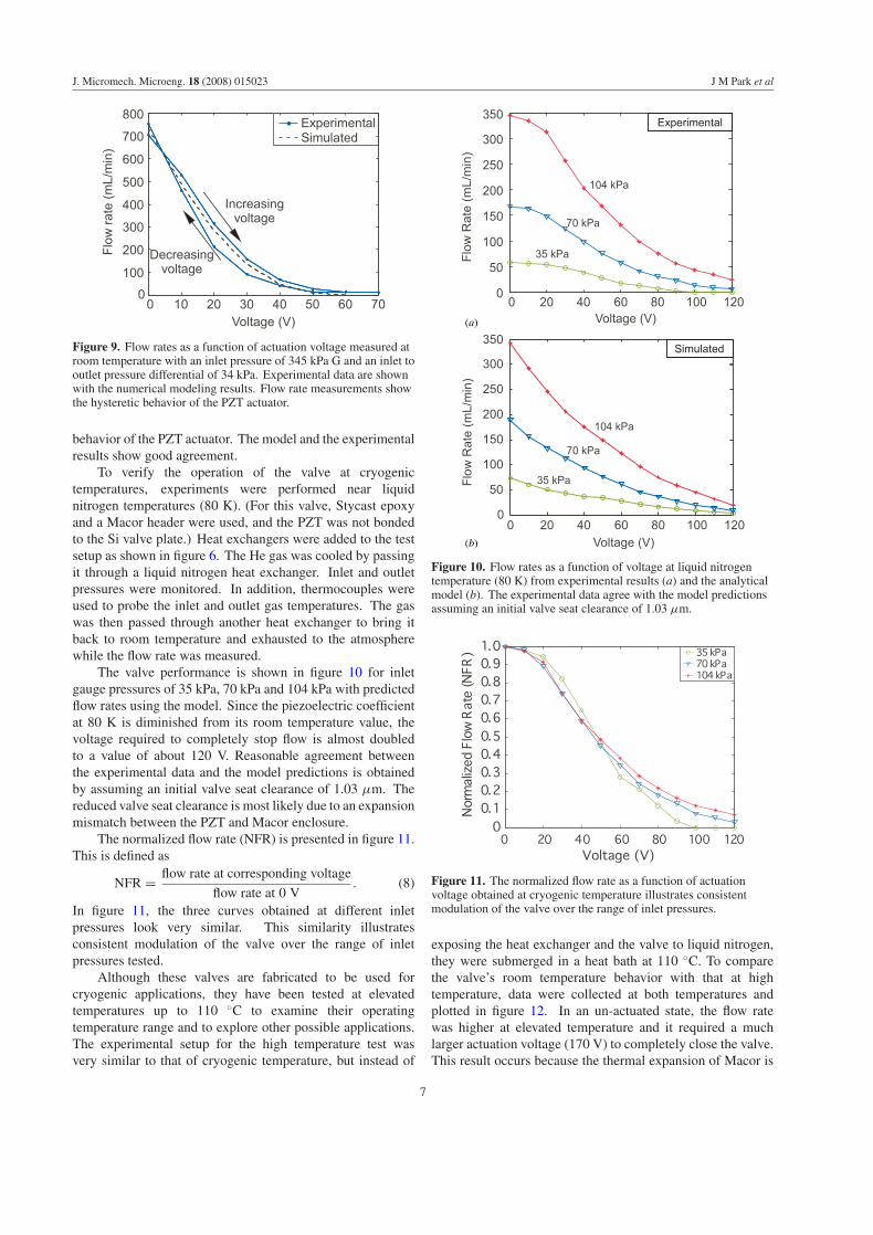
throttling valves were utilized downstream of the valve toallow precise regulation of the pressure difference at highabsolute line pressure. Tests were conducted by holdingthe inlet pressure and differential pressure constants whileincreasing the valve actuation voltage from 0 to 100 V, andthen reducing voltage back to 0 V in 10 V increments. Thetest result comparison with the model prediction is shown infigure 9. The flow rate measurements reveal the hysteretic
6
J. Micromech. Microeng. 18 (2008) 015023 J M Park et al
Figure 9. Flow rates as a function of actuation voltage measured atroom temperature with an inlet pressure of 345 kPa G and an inlet tooutlet pressure differential of 34 kPa. Experimental data are shownwith the numerical modeling results. Flow rate measurements showthe hysteretic behavior of the PZT actuator.
behavior of the PZT actuator. The model and the experimentalresults show good agreement.
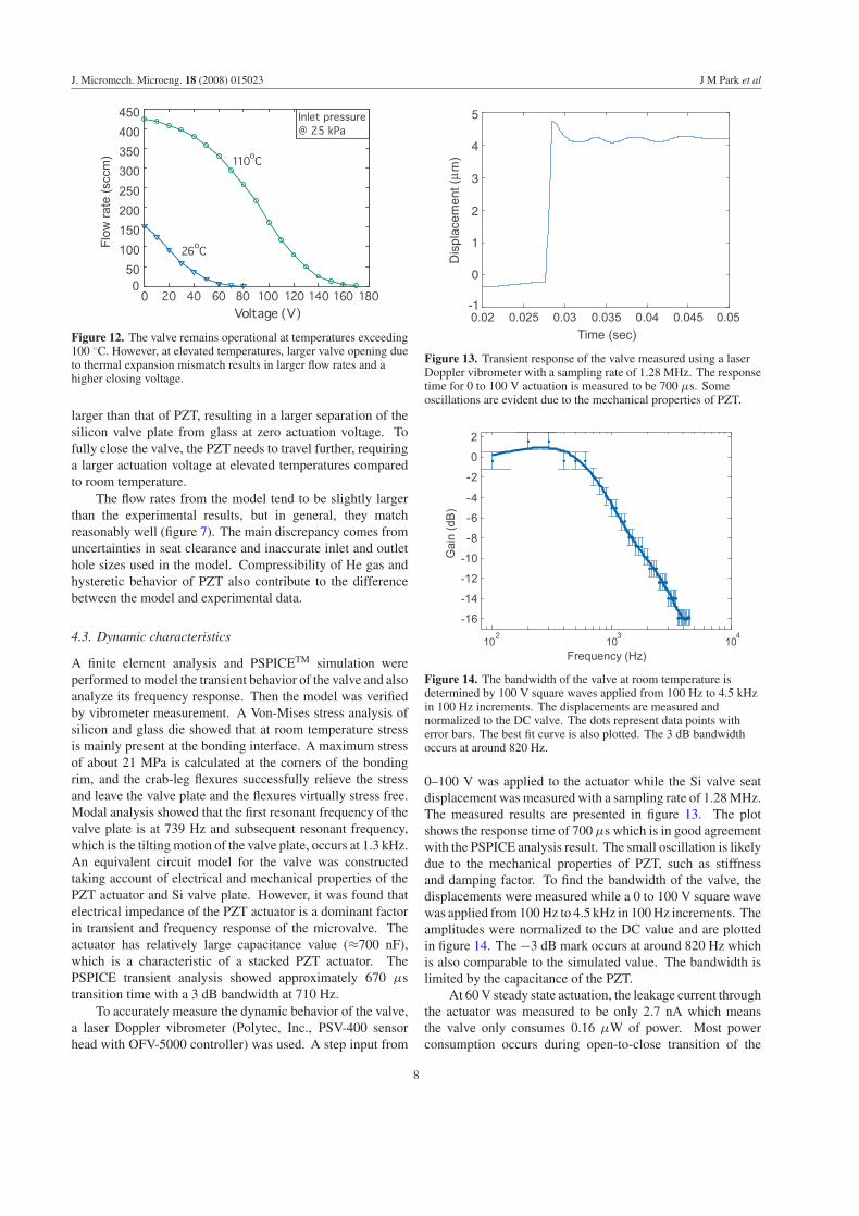
To verify the operation of the valve at cryogenictemperatures, experiments were performed near liquidnitrogen temperatures (80 K). (For this valve, Stycast epoxyand a Macor header were used, and the PZT was not bondedto the Si valve plate.) Heat exchangers were added to the testsetup as shown in figure 6. The He gas was cooled by passingit through a liquid nitrogen heat exchanger. Inlet and outletpressures were monitored. In addition, thermocouples wereused to probe the inlet and outlet gas temperatures. The gaswas then passed through another heat exchanger to bring itback to room temperature and exhausted to the atmospherewhile the flow rate was measured.
The valve performance is shown in figure 10 for inletgauge pressures of 35 kPa, 70 kPa and 104 kPa with predictedflow rates using the model. Since the piezoelectric coefficientat 80 K is diminished from its room temperature value, thevoltage required to completely stop flow is almost doubledto a value of about 120 V. Reasonable agreement betweenthe experimental data and the model predictions is obtainedby assuming an initial valve seat clearance of 1.03 µm. Thereduced valve seat clearance is most likely due to an expansionmismatch between the PZT and Macor enclosure.
The normalized flow rate (NFR) is presented in figure 11.This is defined as
NFR = flow rate at corresponding voltage
flow rate at 0 V. (8)
In figure 11, the three curves obtained at different inletpressures look very similar. This similarity illustratesconsistent modulation of the valve over the range of inletpressures tested.
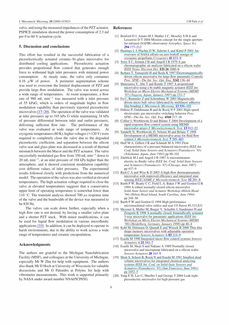
Although these valves are fabricated to be used forcryogenic applications, they have been tested at elevatedtemperatures up to 110 ◦C to examine their operatingtemperature range and to explore other possible applications.The experimental setup for the high temperature test wasvery similar to that of cryogenic temperature, but instead of
(a)
(b)
Figure 10. Flow rates as a function of voltage at liquid nitrogentemperature (80 K) from experimental results (a) and the analyticalmodel (b). The experimental data agree with the model predictionsassuming an initial valve seat clearance of 1.03 µm.
Figure 11. The normalized flow rate as a function of actuationvoltage obtained at cryogenic temperature illustrates consistentmodulation of the valve over the range of inlet pressures.
exposing the heat exchanger and the valve to liquid nitrogen,they were submerged in a heat bath at 110 ◦C. To comparethe valve’s room temperature behavior with that at hightemperature, data were collected at both temperatures andplotted in figure 12. In an un-actuated state, the flow ratewas higher at elevated temperature and it required a muchlarger actuation voltage (170 V) to completely close the valve.This result occurs because the thermal expansion of Macor is
7
J. Micromech. Microeng. 18 (2008) 015023 J M Park et al
Figure 12. The valve remains operational at temperatures exceeding100 ◦C. However, at elevated temperatures, larger valve opening dueto thermal expansion mismatch results in larger flow rates and ahigher closing voltage.
larger than that of PZT, resulting in a larger separation of thesilicon valve plate from glass at zero actuation voltage. Tofully close the valve, the PZT needs to travel further, requiringa larger actuation voltage at elevated temperatures comparedto room temperature.
The flow rates from the model tend to be slightly largerthan the experimental results, but in general, they matchreasonably well (figure 7). The main discrepancy comes fromuncertainties in seat clearance and inaccurate inlet and outlethole sizes used in the model. Compressibility of He gas andhysteretic behavior of PZT also contribute to the differencebetween the model and experimental data.
4.3. Dynamic characteristics
A finite element analysis and PSPICETM simulation wereperformed to model the transient behavior of the valve and alsoanalyze its frequency response. Then the model was verifiedby vibrometer measurement. A Von-Mises stress analysis ofsilicon and glass die showed that at room temperature stressis mainly present at the bonding interface. A maximum stressof about 21 MPa is calculated at the corners of the bondingrim, and the crab-leg flexures successfully relieve the stressand leave the valve plate and the flexures virtually stress free.Modal analysis showed that the first resonant frequency of thevalve plate is at 739 Hz and subsequent resonant frequency,which is the tilting motion of the valve plate, occurs at 1.3 kHz.An equivalent circuit model for the valve was constructedtaking account of electrical and mechanical properties of thePZT actuator and Si valve plate. However, it was found thatelectrical impedance of the PZT actuator is a dominant factorin transient and frequency response of the microvalve. Theactuator has relatively large capacitance value (≈700 nF),which is a characteristic of a stacked PZT actuator. ThePSPICE transient analysis showed approximately 670 µstransition time with a 3 dB bandwidth at 710 Hz.
To accurately measure the dynamic behavior of the valve,a laser Doppler vibrometer (Polytec, Inc., PSV-400 sensorhead with OFV-5000 controller) was used. A step input from
-1
0
1
2
3
4
5
Dis
plac
emen
t (µ
Figure 13. Transient response of the valve measured using a laserDoppler vibrometer with a sampling rate of 1.28 MHz. The responsetime for 0 to 100 V actuation is measured to be 700 µs. Someoscillations are evident due to the mechanical properties of PZT.
Figure 14. The bandwidth of the valve at room temperature isdetermined by 100 V square waves applied from 100 Hz to 4.5 kHzin 100 Hz increments. The displacements are measured andnormalized to the DC valve. The dots represent data points witherror bars. The best fit curve is also plotted. The 3 dB bandwidthoccurs at around 820 Hz.
0–100 V was applied to the actuator while the Si valve seatdisplacement was measured with a sampling rate of 1.28 MHz.The measured results are presented in figure 13. The plotshows the response time of 700 µs which is in good agreementwith the PSPICE analysis result. The small oscillation is likelydue to the mechanical properties of PZT, such as stiffnessand damping factor. To find the bandwidth of the valve, thedisplacements were measured while a 0 to 100 V square wavewas applied from 100 Hz to 4.5 kHz in 100 Hz increments. Theamplitudes were normalized to the DC value and are plottedin figure 14. The −3 dB mark occurs at around 820 Hz whichis also comparable to the simulated value. The bandwidth islimited by the capacitance of the PZT.
At 60 V steady state actuation, the leakage current throughthe actuator was measured to be only 2.7 nA which meansthe valve only consumes 0.16 µW of power. Most powerconsumption occurs during open-to-close transition of the
8
J. Micromech. Microeng. 18 (2008) 015023 J M Park et al
valve, and using the measured impedances of the PZT actuator,PSPICE simulation showed the power consumption of 2.3 mJper 0 to 60 V actuation cycle.
5. Discussion and conclusions
This effort has resulted in the successful fabrication of apiezoelectrically actuated ceramic–Si–glass microvalve fordistributed cooling applications. Piezoelectric actuationprovides proportional flow control that generates enoughforce to withstand high inlet pressures with minimal powerconsumption. At steady state, the valve only consumes0.16 µW of power. A perimeter augmentation schemewas used to overcome the limited displacement of PZT andprovide large flow modulation. The valve was tested acrossa wide range of temperatures. At room temperature, a flowrate of 980 mL min−1 was measured with a inlet pressureof 55 kPaG, which is orders of magnitude higher in flowmodulation capability than previously reported piezoelectricmicrovalves [17–20]. The operation of the valve was validatedat inlet pressures up to 345 kPa G while maintaining 34 kPaof pressure differential between inlet and outlet pressures,delivering sufficient flow rate. The performance of thevalve was evaluated at wide range of temperatures. Atcryogenic temperatures (80 K), higher voltages (≈120 V) wererequired to completely close the valve due to the degradedpiezoelectric coefficient, and separation between the siliconvalve seat and glass plate was decreased as a result of thermalmismatch between the Macor and the PZT actuator. The valvesuccessfully modulated gas flow from 350 mL min−1 down to20 mL min−1, at an inlet pressure of 104 kPa higher than theatmosphere, and it showed consistent modulation capabilityover different values of inlet pressures. The experimentalresults followed closely with predictions from the numericalmodel. The operation of the valves was also verified at elevatedtemperatures. The high actuation voltage required to close thevalve at elevated temperatures suggests that a conservativeupper limit of operating temperature is somewhat lower than110 ◦C. The transient analysis showed 700 µs response timeof the valve and the bandwidth of the device was measured tobe 820 Hz.
The valves can scale down further, especially when ahigh flow rate is not desired, by having a smaller valve plateand a shorter PZT stack. With minor modifications, it canbe used for liquid flow modulation in various microfluidicapplications [33]. In addition, it can be deployed to operate inharsh environments, due to the ability to work across a widerange of temperatures and ceramic encapsulation.
Acknowledgments
The authors are grateful to the Michigan NanofabricationFacility (MNF), and colleagues at the University of Michigan,especially Mr W Zhu for help with equipment. The authorsalso thank Mr D Hoch at University of Wisconsin for valuablediscussions and Mr G Palombo at Polytec for help withvibrometer measurements. This work is supported primarilyby NASA under award number NNA05CP85G.
References
[1] Benford D J, Amato M J, Mather J C, Moseley S H Jr andLeisawitz D T 2004 Mission concept for the single aperturefar-infrared (SAFIR) observatory Astrophys. Space Sci.294 177–212
[2] Hastings L J, Plachta D W, Salerno L and Kittel P 2001 Anoverview of NASA efforts on zero boiloff storage ofcryogenic propellants Cryogenics 41 833–9
[3] Terry S C, Jerman J H and Angell J B 1979 A gaschromatographic air analyzer fabricated on a silicon waferIEEE Trans. Electron Dev. ED-26 1880–6
[4] Ikehara T, Yamagishi H and Ikeda K 1997 Electromagneticallydriven silicon microvalve for large-flow pneumatic ControlsProc. SPIE—The Int. Soc. Opt. Eng. 3242 136–44
[5] Shinozawa Y, Abe T and Kondo T 1997 A proportionalmicrovalve using a bi-stable magnetic actuator IEEE Int.Workshop on Micro Electro Mechanical Systems (MEMS’97) (Nagoya, Japan, January 1997) pp 233–7
[6] Fu C, Rummler Z and Schomburg W 2003 Magneticallydriven micro ball valves fabricated by multilayer adhesivefilm bonding J. Micromech. Microeng. 13 S96–102
[7] Dubois P, Guldimann B and de Rooij N F 2001 High-speedelectrostatic gas microvalve switching behavior Proc.SPIE—The Int. Soc. Opt. Eng. 4560 217–26
[8] Collier J, Wroblewski D and Bifano T 2004 Development of arapid-response flow-control system using MEMSmicrovalve arrays J. Microelectromech. Syst. 13 912–22
[9] Vandelli N, Wroblewski D, Velonis M and Bifano T 1998Development of a MEMS microvalve array for fluid flowcontrol J. Microelectromech. Syst. 7 395–403
[10] Huff M A, Gilbert J R and Schmidt M A 1993 Flowcharacteristics of a pressure-balanced microvalve IEEE Int.Conf. Solid-State Sensors and Actuators (Transducers ’93)(Yokohama, Japan, June 1993) pp 98–101
[11] Zdeblick M J and Angell J B 1987 A microminiatureelectric-to-fluidic valve IEEE Int. Conf. Solid-State Sensorsand Actuators (Transducers ’87) (Chicago, June 1987)pp 437–9
[12] Rich C A and Wise K D 2003 A high-flow thermopneumaticmicrovalve with improved efficiency and integrated statesensing IEEE/ASME J. Microelectromech. Syst. 12 201–8
[13] Barth P W, Beatty C C, Field L A, Baker J W and Gordon G B1994 A robust normally-closed silicon microvalveSolid-State Sensor and Actuator Workshop (Hilton Head’94) (Hilton Head Island, South Carolina, June 1994)pp 248–50
[14] Barth P W and Gordon G 1994 High performancemicromachined valve orifice and seat US Patent #5,333,831
[15] Messner S, Muller M, Burger V, Schaible J, Sandmaier H andZengerle R 1998 A normally-closed, bimetallically actuated3-way microvalve for pneumatic applications IEEE Int.Workshop on Micro Electro Mechanical Systems (MEMS’98) (Heidelberg, Germany, January 1998) pp 40–4
[16] Kohl M, Dittmann D, Quandt E and Winzek B 2000 Thin filmshape memory microvalves with adjustable operationtemperature Sensors Actuators A 83 214–9
[17] Esashi M 1990 Integrated micro flow control systems SensorsActuators A 21 161–7
[18] Esashi M, Shoji S and Nakano A 1989 Normally closedmicrovalve and micropump fabricated on a silicon waferSensors Actuators 20 163–9
[19] Shoji S, Schoot B, Rooij N and Esashi M 1991 Smallest deadvolume microvalves for integrated chemical analyzingsystems IEEE Int. Conf. on Solid-State Sensors andActuators (Transducers ’91) (San Francisco, June 1991)pp 1052–5
[20] Yang E H, Lee C, Mueller J and George T 2004 Leak-tightpiezoelectric microvalve for high-pressure gas
9

J. Micromech. Microeng. 18 (2008) 015023 J M Park et al
micropropulsion IEEE J. Microelectromech. Syst.13 799–807
[21] Chakraborty I, Tang W C, Bame D P and Tang T K 2000MEMS micro-valve for space application Sensors ActuatorsA 83 188–93
[22] Roberts D C, Hanqing L, Steyn J L, Yaglioglu O,Spearing S M, Schmidt M A and Hagood N W 2003 Apiezoelectric microvalve for compact high-frequency,high-differential pressure hydraulic micropumping systemsIEEE J. Microelectromech. Syst. 12 81–92
[23] Rogge T, Rummler Z and Schomburg W K 2004 Polymermicro valve with a hydraulic piezo-drive fabricatedby the AMANDA process Sensors Actuators A110 206–12
[24] Park J M, Taylor R P, Evans A T, Brosten T R, Nellis G F,Klein S A, Feller J R, Salerno L and Gianchandani Y B2006 A piezoelectrically actuated ceramic-Si-glassmicrovalve for distributed cooling systems Solid-StateSensor and Actuator Workshop (Hilton Head ’06)(Hilton Head Island, South Carolina, June 2006) pp 248–51
[25] Gerson R 1962 Piezoelectric and dielectric properties of leadtitanate zirconate ceramics at low temperatures J. Appl.Phys. 33 830–2
[26] Taylor R P, Nellis G F, Klein S A, Hoch D W, Feller J,Roach P, Park J M and Gianchandani Y 2005Measurements of the material properties of a laminatedpiezoelectric stack at cryogenic temperatures 30th Int.Cryogenic Materials Conf. (Keystone, Colorado, Aug.29–Sept. 2 2005) pp 200–7
[27] Taylor R P 2005 A micromachined croyogenic valve fordistributed cooling applications MS Thesis The Universityof Wisconsin, Madison
[28] Andersen B A M, Hansen O and Kristensen M 1997 Spatialvariation of the etch rate for deep etching of silicon byreactive ion etching J. Vac. Sci. Technol. B 15 993–9
[29] Taylor H K, Sun H, Hill T F, Farahanchi A and Boning D S2006 Characterizing and predicting spatial nonuniformity inthe deep reactive ion etching of silicon J. Electrochem. Soc.153 C575–85
[30] Fascio V, Wuthrich R, Viquerat D and Langen H 1999 3Dmicrostructuring of glass using electrochemical dischargemachining (ECDM) Int. Symp. Micromechatronics andHuman Science (Nagoya, Japan, Nov. 1999)pp 179–83
[31] Klein S A 2002 Engineering Equation Solver, The Universityof Wisconsin—Madisonhttp://sel.me.wisc.edu/ees/new ees.html
[32] Brosten T R, Park J M, Evans A T, Rasmussen K, Nellis G F,Klein S A, Feller J R, Salerno L and Gianchandani Y B2007 A numerical flow model and experimental results of acryogenic microvalve for distributed cooling applicationsCryogenics 47 501–9
[33] Evans A, Park J M, Taylor R P, Brosten T R, Nellis G F,Klein S A, Feller J R, Salerno L and Gianchandani Y B2006 A low power, micromachined proportional valve fordrug delivery Int. Conf. Miniaturized Chemical andBiochemical Analysis Systems (MicroTAS 2006) (Tokyo,Japan, Nov. 2006) pp 1148–50
10


