Embed Size (px)
Citation preview
Enhanced carrier density in Nb-doped SrTiO3 thermoelectricsK. Ozdogan, M. Upadhyay Kahaly, S. R. Sarath Kumar, H. N. Alshareef, and U. Schwingenschlögl Citation: J. Appl. Phys. 111, 054313 (2012); doi: 10.1063/1.3692057 View online: http://dx.doi.org/10.1063/1.3692057 View Table of Contents: http://jap.aip.org/resource/1/JAPIAU/v111/i5 Published by the American Institute of Physics. Related ArticlesHigh mobility two-dimensional hole system on hydrogen-terminated silicon (111) surfaces Appl. Phys. Lett. 100, 252107 (2012) Electrical and piezoelectric properties of BiFeO3 thin films grown on SrxCa1−xRuO3-buffered SrTiO3 substrates J. Appl. Phys. 111, 114102 (2012) Electrical properties of (110) epitaxial lead-free ferroelectric Na0.5Bi0.5TiO3 thin films grown by pulsed laserdeposition: Macroscopic and nanoscale data J. Appl. Phys. 111, 104106 (2012) Tunable strain effect and ferroelectric field effect on the electronic transport properties of La0.5Sr0.5CoO3 thinfilms J. Appl. Phys. 111, 103702 (2012) Coexistence of unipolar and bipolar resistive switching in BiFeO3 and Bi0.8Ca0.2FeO3 films J. Appl. Phys. 111, 104103 (2012) Additional information on J. Appl. Phys.Journal Homepage: http://jap.aip.org/ Journal Information: http://jap.aip.org/about/about_the_journal Top downloads: http://jap.aip.org/features/most_downloaded Information for Authors: http://jap.aip.org/authors
Downloaded 21 Jun 2012 to 194.27.101.97. Redistribution subject to AIP license or copyright; see http://jap.aip.org/about/rights_and_permissions
Enhanced carrier density in Nb-doped SrTiO3 thermoelectrics
K. Ozdogan,1,2 M. Upadhyay Kahaly,1 S. R. Sarath Kumar,1 H. N. Alshareef,1
and U. Schwingenschlogl1,a)
1KAUST, Physical Science & Engineering, Thuwal 23955-6900, Kingdom of Saudi Arabia2Department of Physics, Yildiz Technical University, 34210 Istanbul, Turkey
(Received 13 January 2012; accepted 3 February 2012; published online 8 March 2012)
We study epitaxial SrTiO3 interfaced with Nb-doped SrTi1-xNbxO3 (x¼ 0, 0.125, 0.25, 0.375, and
0.5) by full-potential density functional theory. From the electronic band structures obtained by our
ab-initio calculations we determine the dependence of the induced metallicity on the Nb
concentration. We obtain a monotonous increase of the carrier density with the Nb concentration.
The results are confirmed by experiments for SrTi0.88Nb0.12O3 and SrTi0.8Nb0.2O3, demonstrating
the predictive power and limitations of our theoretical approach. We also show that the Seebeck
coefficient decreases monotonously with increasing temperature. VC 2012 American Institute ofPhysics. [http://dx.doi.org/10.1063/1.3692057]
I. INTRODUCTION
Perovskite oxides with the general formula ABO3, where
A and B denote large and small cations, respectively, have
been investigated extensively since they exhibit rich physical
and chemical phenomena, e.g., piezoelectricity, ferroelectric-
ity, and ferromagnetism. This makes them attractive materi-
als for field effect transistors, non-volatile memories,
piezoelectric transducers, and optical waveguides.1–3 Stron-
tium titanate (SrTiO3; STO) is one of the most widely used
cubic perovskite oxides, owing to its chemically and compo-
sitionally stable structure and small lattice mismatch with
other perovskite oxides.4–6 It finds a wide range of applica-
tions in non-volatile resistive switching memories,7,8 field
effect transistors,9 and memory storage devices.10 The elec-
tronic structure of STO as obtained by reflectivity measure-
ments reveals a band insulator with a bandgap of 3.2 eV at
room temperature.11
Even under slight n or p-doping the electronic properties
of STO are modified drastically.12–15 For example, STO
shows superconductivity at low temperature (Tc < 0.3 K)
when Ti is partially substituted by Nb.16 It has already been
demonstrated that during synthesis of Nb-doped STO, Nb5þ
ions occupy the Ti sites and contribute to the metallicity in
the otherwise insulating material.17 When a Nb-doped STO
film is grown on pure STO, the interface states are influenced
by the n-type Nb5þ donors. Only very few theoretical studies
have been reported for Nb-doped STO, all of them dealing
with bulk systems. In Ref. 18, the structure relaxation due to
the Nb dopant and formation energies have been discussed,
while Refs. 19 and 20 deal with the effective mass and con-
ductivity. In addition, the transport properties have been
investigated in Ref. 21. A profound understanding of how the
charge carrier density changes with the Nb positions and con-
centration is crucial for controlling the overall electrical con-
ductivity of Nb-doped STO films and utilizing them for
technological applications, for example, in thermoelectrics.
In this paper, we address the above issues by both density
functional theory based calculations and experiments. While
the experimental findings focus on the variation of the electri-
cal conductivity and Seebeck coefficient with the temperature
in Nb-doped STO films with two fixed Nb concentrations, we
extrapolate this knowledge for varying Nb concentrations by
our simulations. Our results demonstrate that Nb doping
yields an increase of the carrier concentration and decrease of
the thermoelectric response in STO based oxides.
II. METHODOLOGY
A. Experimental
Thin films of Nb-doped STO were deposited on a LaAlO3
substrate, held at a temperature of 700 �C, by pulsed laser dep-
osition of SrTi0.85Nb0.15O3 and SrTi0.80Nb0.20O3 targets. A
KrF excimer laser (248 nm) at a power density of 75 W cm�2
was used for ablation in the presence of Ar gas (20 mTorr).
The electrical resistivity of the film was measured in the tem-
perature range from 5 to 350 K using a physical property mea-
surement system (PPMS, Quantum Design, USA) and in the
high temperature range from 300 to 900 K using a linear four
probe technique (RZ2001i, Ozawa Sciences, Japan). The high
temperature (300 to 900 K) Seebeck coefficient was also
measured by the RZ2001i, using the steady state method. A
temperature difference of less than 4 K was maintained in the
Seebeck coefficient measurements. The room temperature car-
rier concentration was measured using a PPMS by sweeping
the applied magnetic field (50 kOe) under a steady current of
20 A in a rectangular Hall geometry. The composition of the
films was measured by high-resolution Rutherford backscat-
tering Spectrometry (HRBS-500, Kobelco, Japan). In order to
reduce the influence of O vacancies, the films were further
annealed in an Ar/air mixture in a furnace by slowly increas-
ing the temperature up to 700 �C (ramp rate of 5 �C per mi-
nute) and then cooling back to room temperature in 14 hrs.
B. Computational
We use the full-potential linearized augmented plane
wave plus local orbitals method as implemented in thea)Electronic mail: [email protected].
0021-8979/2012/111(5)/054313/5/$30.00 VC 2012 American Institute of Physics111, 054313-1
JOURNAL OF APPLIED PHYSICS 111, 054313 (2012)
Downloaded 21 Jun 2012 to 194.27.101.97. Redistribution subject to AIP license or copyright; see http://jap.aip.org/about/rights_and_permissions
WIEN2k code,22 within the framework of density functional
theory. To vary the dopant concentration from x¼ 12.5% to
50% in SrTi1-xNbxO3, the supercell approach is used23–26
with a 2� 2� 6 supercell (120 atoms in total) of the primi-
tive cubic unit cell, where 4 STO layers are considered to be
the substrate (see the structure in Fig. 1). The Brillouin zone
is sampled on a Monkhorst-Pack 6� 6� 2 k-space grid. We
take into account the relativistic effects for the core states,
but use the scalar relativistic approximation for the valence
states so that spin-orbit coupling is not included. The
exchange-correlation potential is treated in the local density
(LDA) and the generalized gradient (GGA) approximations.
For the wave function expansion inside the atomic spheres,
we choose a maximum value of lmax¼ 12 and employ a
plane-wave cutoff of RmtKmax¼ 6 with Gmax¼ 24. The
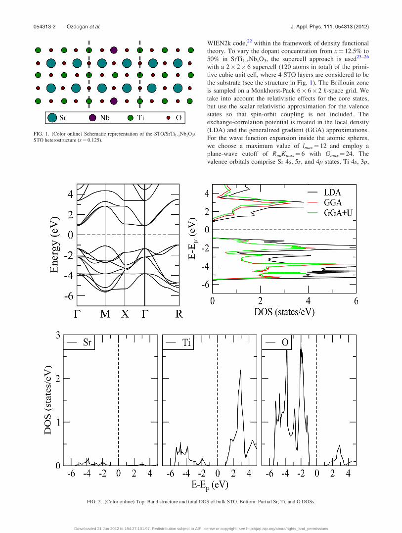
valence orbitals comprise Sr 4s, 5s, and 4p states, Ti 4s, 3p,
FIG. 1. (Color online) Schematic representation of the STO/SrTi1-xNbxO3/
STO heterostructure (x¼ 0.125).
FIG. 2. (Color online) Top: Band structure and total DOS of bulk STO. Bottom: Partial Sr, Ti, and O DOSs.
054313-2 Ozdogan et al. J. Appl. Phys. 111, 054313 (2012)
Downloaded 21 Jun 2012 to 194.27.101.97. Redistribution subject to AIP license or copyright; see http://jap.aip.org/about/rights_and_permissions
and 3d states, Nb 5s, 4p, and 4d states, and O 2s and 2pstates. All lower states are treated as semi-core and core
states. The values of the muffin-tin sphere radii (in atomic
units) are taken to be 2.50 for Sr, 1.94 for Ti and Nb, and
1.60 for O. All calculation parameters have been checked
carefully for convergence to obtain correct results. To cap-
ture the effects of structural relaxation on the local chemical
bonding and physical properties, the atomic forces in the
supercell have been converged down to less than 1 mRy. In
order to avoid strong Nb-Nb repulsion, we choose distances
between the Nb atoms of more than 5.5 A for all doping con-
centrations. Moreover, we apply the experimental lattice
constant of SrTiO3 (a¼ 3.905 A). To predict the Seebeck
coefficient we employ the BoltzTraP code27 which is inter-
faced with WIEN2k. This code is based on Boltzmann theory
and provides estimates of band structure dependent quanti-
ties (such as the electrical and thermal conductivity) within
the rigid band approach.
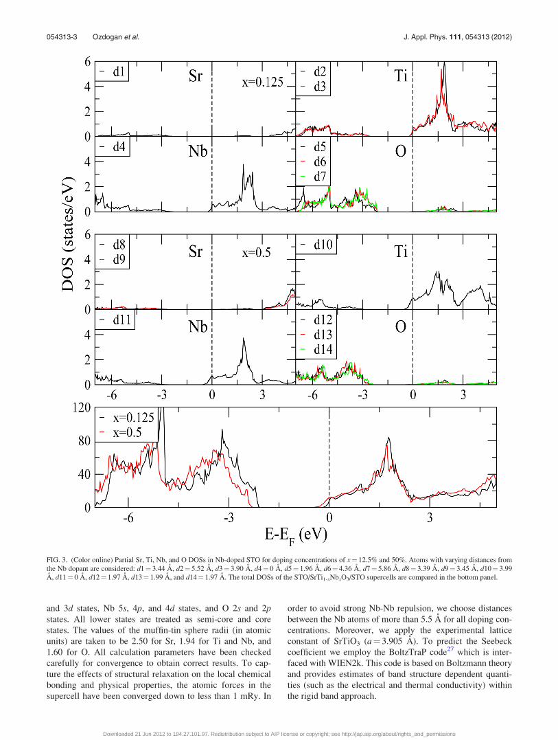
FIG. 3. (Color online) Partial Sr, Ti, Nb, and O DOSs in Nb-doped STO for doping concentrations of x¼ 12.5% and 50%. Atoms with varying distances from
the Nb dopant are considered: d1¼ 3.44 A, d2¼ 5.52 A, d3¼ 3.90 A, d4¼ 0 A, d5¼ 1.96 A, d6¼ 4.36 A, d7¼ 5.86 A, d8¼ 3.39 A, d9¼ 3.45 A, d10¼ 3.99
A, d11¼ 0 A, d12¼ 1.97 A, d13¼ 1.99 A, and d14¼ 1.97 A. The total DOSs of the STO/SrTi1-xNbxO3/STO supercells are compared in the bottom panel.
054313-3 Ozdogan et al. J. Appl. Phys. 111, 054313 (2012)
Downloaded 21 Jun 2012 to 194.27.101.97. Redistribution subject to AIP license or copyright; see http://jap.aip.org/about/rights_and_permissions
III. RESULTS AND DISCUSSION
Bulk STO is found to be insulating, compare the band
structure in the top left panel of Fig. 2. The GGA bandgap is
1.9 eV, which is a well known underestimation with respect
to the experimental value of 3.2 eV (Ref. 11) and in a good
agreement with previous numerical findings.28 The results
for the total density of states (DOS) of bulk STO from our
LDA, GGA, and GGAþU (with U¼ 6 eV) calculations are
shown in the top right panel of Fig. 2. They suggest that (i)
the LDA gap is smaller than the GGA gap by about 0.15 eV
and (ii) the bandgap can hardly be improved by inclusion of
the on-site interaction U. Hence, for all further calculations
we use the GGA. Partial Sr, Ti, and O DOSs for pristine
STO (bottom panels of Fig. 2) show that while the highest
occupied molecular orbital is due to the O 2p states, the low-
est unoccupied molecular orbital originates from the Ti 3d
states. Sr hardly contributes in the energy range around the
Fermi level.
We have calculated the DOS of the STO/SrTi1�xNbxO3/
STO heterostructures for x¼ 0.125, 0.25, 0.375, and 0.5 to
demonstrate the effect of Nb doping on the electronic struc-
ture of the system. The total and partial DOSs are shown in
Fig. 3. The partial Ti and O DOSs of bulk STO (Fig. 2, bot-
tom panel) are drastically modified in the presence of a Nb
dopant. While the main contribution to the top of the valence
band is due to the O 2p states with some admixtures from the
Ti 3d and Nb 4d states, the main contribution to the bottom
of the conduction band originates from the Ti 3d and Nb 4d
states with admixtures from the O 2p states. Thus, the Nb
ions contribute more to the conduction band than to the va-
lence band. When we increase the Nb concentration, the
gross shape of the DOS remains similar, but it shifts to lower
energy (see Fig. 3, bottom panel). Due to hybridization with
the Nb dopant, the 2p states of neighboring O atoms contrib-
ute slightly at the Fermi energy. In addition, for x¼ 0.125
the O 2p DOS is altered, especially in the valence band,
depending on the O-Nb distance (see the three O atoms with
distances d5, d6, and d7, for example). These O atoms hy-
bridize a weakly with Ti and Nb, which experience strong
hybridization with each other. Irrespective of the Nb-Sr dis-
tance, the Sr DOS remains mostly unchanged.
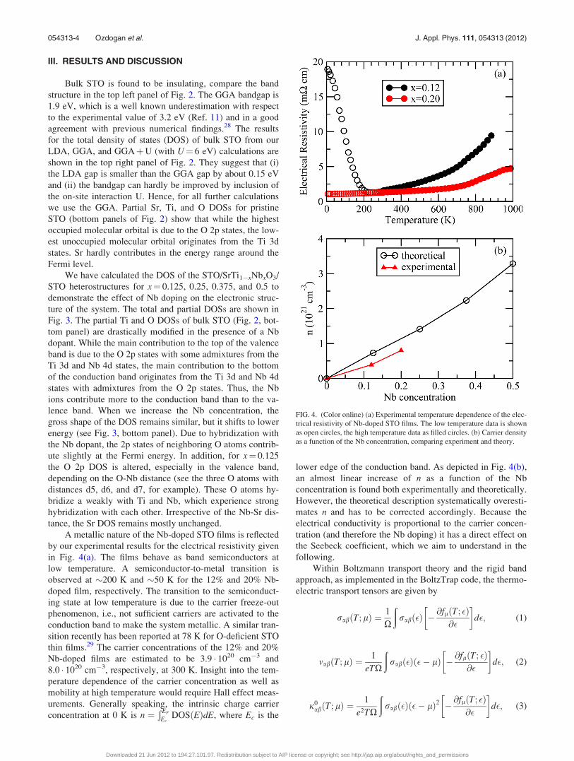
A metallic nature of the Nb-doped STO films is reflected
by our experimental results for the electrical resistivity given
in Fig. 4(a). The films behave as band semiconductors at
low temperature. A semiconductor-to-metal transition is
observed at �200 K and �50 K for the 12% and 20% Nb-
doped film, respectively. The transition to the semiconduct-
ing state at low temperature is due to the carrier freeze-out
phenomenon, i.e., not sufficient carriers are activated to the
conduction band to make the system metallic. A similar tran-
sition recently has been reported at 78 K for O-deficient STO
thin films.29 The carrier concentrations of the 12% and 20%
Nb-doped films are estimated to be 3.9 � 1020 cm�3 and
8.0 � 1020 cm�3, respectively, at 300 K. Insight into the tem-
perature dependence of the carrier concentration as well as
mobility at high temperature would require Hall effect meas-
urements. Generally speaking, the intrinsic charge carrier
concentration at 0 K is n ¼Ð EF
EcDOSðEÞdE, where Ec is the
lower edge of the conduction band. As depicted in Fig. 4(b),
an almost linear increase of n as a function of the Nb
concentration is found both experimentally and theoretically.
However, the theoretical description systematically overesti-
mates n and has to be corrected accordingly. Because the
electrical conductivity is proportional to the carrier concen-
tration (and therefore the Nb doping) it has a direct effect on
the Seebeck coefficient, which we aim to understand in the
following.
Within Boltzmann transport theory and the rigid band
approach, as implemented in the BoltzTrap code, the thermo-
electric transport tensors are given by
rabðT; lÞ ¼ 1
X
ðrabð�Þ �
@flðT; �Þ@�
� �d�; (1)
vabðT; lÞ ¼ 1
eTX
ðrabð�Þð�� lÞ � @flðT; �Þ
@�
� �d�; (2)
j0abðT; lÞ ¼ 1
e2TX
ðrabð�Þð�� lÞ2 � @flðT; �Þ
@�
� �d�; (3)
FIG. 4. (Color online) (a) Experimental temperature dependence of the elec-
trical resistivity of Nb-doped STO films. The low temperature data is shown
as open circles, the high temperature data as filled circles. (b) Carrier density
as a function of the Nb concentration, comparing experiment and theory.
054313-4 Ozdogan et al. J. Appl. Phys. 111, 054313 (2012)
Downloaded 21 Jun 2012 to 194.27.101.97. Redistribution subject to AIP license or copyright; see http://jap.aip.org/about/rights_and_permissions
where r is the electrical conductivity, j0 is the electronic
part of the thermal conductivity, f is the Fermi-Dirac distri-
bution function, l is the chemical potential, and T is the tem-
perature (a, b¼ 1, 2, 3). The Seebeck coefficient Sij is given
by the electric field Ei and temperature gradient as
Sij ¼ EiðrjTÞ�1 ¼ ðr�1Þaivaj: (4)
Taking into account the symmetry of the system (Sij¼ Sji),
the principal Seebeck coefficient can be expressed as
S¼ r�1 �, where r and � are estimated using the rigid band
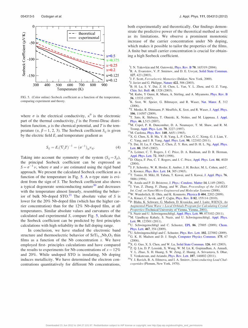
approach. We present the calculated Seebeck coefficient as a
function of the temperature in Fig. 5. A n-type state is evi-
dent from the sign of S. The Seebeck coefficient also shows
a typical degenerate semiconducting nature30 and decreases
with the temperature almost linearly, resembling the behav-
ior of bulk Nb-doped STO.21 The absolute value of S is
lower for the 20% Nb-doped film (which has the higher car-
rier concentration) than for the 12% Nb-doped film, at all
temperatures. Similar absolute values and curvatures of the
calculated and experimental S, compare Fig. 5, indicate that
the Seebeck coefficient can be predicted by first principles
calculations with high reliability in the full doping range.
In conclusion, we have studied the electronic band
structure and thermoelectric behavior of SrTi1-xNbxO3 thin
films as a function of the Nb concentration x. We have
employed first- principles calculations and have compared
the results to experiments for Nb concentrations of x¼ 12%
and 20%. While undoped STO is insulating, Nb doping
induces metallicity. We have determined the electron con-
centrations quantitatively for different Nb concentrations,
both experimentally and theoretically. Our findings demon-
strate the predictive power of the theoretical method as well
as its limitations. We observe a prominent monotonic
increase of the carrier concentration under Nb doping,
which makes it possible to tailor the properties of the films.
A finite but small carrier concentration is crucial for obtain-
ing a high Seebeck coefficient.
1I. N. Yakovkin and M. Gutowski, Phys. Rev. B 70, 165319 (2004).2R. A. Evarestov, V. P. Smirnov, and D. E. Usvyat, Solid State Commun.
127, 423 (2003).3J. F. Scott, Ferroelectric Memories (Dekker, New York, 2000).4J. Javier and G. Philippe, Nature 422, 506 (2003).5B. H. Lu, S. Y. Dai, Z. H. Chen, L. Yan, Y. L. Zhou, and G. Z. Yang,
Chin. Sci. Bull. 48, 1328 (2003).6M. Kubo, Y Oumi, R. Miura, A. Stirling, and A. Miyamoto, Phys. Rev. B
56, 13535 (1997).7K. Szot, W. Speier, G. Bihmayer, and R. Waser, Nat. Mater. 5, 312
(2006).8T. Menke, R. Dittmann, P. Meuffels, K. Szot, and R. Waser, J. Appl. Phys.
106, 114507 (2009).9T. Sato, K. Shibuya, T. Ohniski, K. Nishio, and M. Lippmaa, J. Appl.
Phys. 46, L515 (2007).10M. Copel, P. R. Duncomber, D. A. Neumayer, T. M. Shaw, and R. M.
Tromp, Appl. Phys. Lett. 70, 3227 (1997).11M. Cardona, Phys. Rev. 140, A651 (1965).12X. G. Chen, X. B. Ma, Y. B. Yang, L. P. Chen, G. C. Xiong, G. J. Lian, Y.
C. Yang, and J. B. Yang, Appl. Phys. Lett. 98, 122102 (2011).13S. Dai, H. Lu, F. Chen, Z. Chen, Z. Y. Ren, and D. H. L. Ng, Appl. Phys.
Lett. 80, 3545 (2002).14A. Leitner, C. T. Rogers, J. C. Price, D. A. Rudman, and D. R. Herman,
Appl. Phys. Lett. 72, 3065 (1998).15D. Olaya, F. Pen, C. T. Rogers, and J. C. Price, Appl. Phys. Lett. 84, 4020
(2004).16J. F. Schooley, W. R. Hosler, E. Amber, J. H. Becker, M. L. Cohen, and C.
S. Koonce, Phys. Rev. Lett. 14, 305 (1965).17T. Tomio, H. Miki, H. Tabata, T. Kawai, and S. Kawai, J. Appl. Phys. 76,
5886 (1994).18R. Astala and P. D. Bristowe, J. Phys.: Condens. Matter 14, L149 (2002).19J. Yun, Z. Zhang, F. Zhang, and W. Zhao, Proceedings of the 3rd IEEE
Int. Conf. on Nano/Micro Engineered and Molecular Systems (2008).20W. Wunderlich, H. Ohta, and K. Koumoto, Physica B 404, 2202 (2009).21A. Kinaci, C. Sevik, and T. Cagin, Phys. Rev. B 82, 155114 (2010).22P. Blaha, K. Schwarz, G. Madsen, D. Kvasicka, and J. Luitz, WIEN2k, An
Augmented Plane WaveþLocal Orbitals Program for Calculating CrystalProperties (Technical University of Vienna, Vienna, 2001).
23S. Nazir and U. Schwingenschlogl, Appl. Phys. Lett. 99, 073102 (2011).24M. Upadhyay Kahaly, S. Nazir, and U. Schwingenschlogl, Appl. Phys.
Lett. 99, 123501 (2011).25U. Schwingenschlogl and C. Schuster, EPL 86, 27005 (2009); Chem.
Phys. Lett. 467, 354 (2009).26U. Schwingenschlogl and C. Schuster, Phys. Rev. Lett. 102, 227002 (2009).27G. K. H. Madsen and D. J. Singh, Computer Physics Commun. 175, 67
(2006).28X. G. Guo, X. S. Chen, and W. Lu, Solid State Commun. 126, 441 (2003).29Z. Q. Liu, D. P. Leusink, X. Wang, W. M. Lu, K. Gopinadhan, A. Annadi,
Y. L. Zhao, X. H. Huang, S. W. Zeng, Z. Huang, A. Srivastava, S. Dhar,
T. Venkatesan, and Ariando, Phys. Rev. Lett. 107, 146802 (2011).30Y. I. Ravich, B. A. Efimova, and I. A. Smirov, Semiconducting Lead Chal-
cogenides (Plenum, New York, 1970).
FIG. 5. (Color online) Seebeck coefficient as a function of the temperature,
comparing experiment and theory.
054313-5 Ozdogan et al. J. Appl. Phys. 111, 054313 (2012)
Downloaded 21 Jun 2012 to 194.27.101.97. Redistribution subject to AIP license or copyright; see http://jap.aip.org/about/rights_and_permissions