Embed Size (px)
Citation preview
C
ATa
b
c
a
ARA
P8777
KPGDX
1
agSrte[atbe
eiSg[d
0d
Materials Chemistry and Physics 115 (2009) 86–92
Contents lists available at ScienceDirect
Materials Chemistry and Physics
journa l homepage: www.e lsev ier .com/ locate /matchemphys
haracterization and properties of microwave plasma-treated SrTiO3
ndrey Shkabkoa, Myriam H. Aguirrea,∗, Ivan Marozaub, Max Doebeli c, Marc Mallepell c,homas Lippertb, Anke Weidenkaff a
Empa, Solid State Chemistry and Catalysis, Ueberlandstrasse 129, 8600 Dübendorf, SwitzerlandPaul Scherrer Institut, 5232 Villigen PSI, SwitzerlandIon Beam Physics, Paul Scherrer Institut and ETH Zurich, 8093 Zurich, Switzerland
r t i c l e i n f o
rticle history:eceived 4 July 2008ccepted 7 November 2008
ACS:2.33Xj7.84 Dy
a b s t r a c t
Nitrogen was successfully incorporated into the surface of a SrTiO3(1 1 1) single crystal by exposing itto a microwave-induced glow discharge plasma of ammonia (NH3). The layers generated by the fluxof active species in the plasma varied in composition and structure depending on the treatment time,t. Substitution of oxygen by nitrogen along with the reduction of the crystal surface was observed byX-ray photoelectron spectroscopy. The 0–150 nm thick top layer showed Sr and O deficiencies and wasidentified as a mixture of nanocrystalline cubic rocksalt-type TiN, perovskite-type SrTiO3−ı–SrTiO3−xNy
9.60−I9.60Jv
eywords:erovskite-type oxynitridelow dischargeiffusion
and amorphous phases. Deeper nitrogen diffusion into the crystal yielded perovskite-type nitrogen-dopedstrontium titanate. The diffusion of N into the perovskite structure was characterized by the diffusioncoefficient D = (2.1 ± 0.4) × 10−15 cm2 s−1. The growth of the N-containing perovskite layers showed the
time dependency L [�m] = 6.3√
t [min]. Examination of the electronic properties revealed metallic-like electrical conductivity, superconductivity with Tc of up to 5 K, and negative Seebeck coefficients ofup to S = −465 �V K−1 at room temperature.
-ray photo-emission spectroscopy (XPS)
. Introduction
SrTiO3 (STO) is a non-conducting material (band insulator) withband gap of 3.2 eV and a cubic perovskite-type structure (space
roup Pm3̄m, unit cell parameter a = 3.905 Å). Surface-reduction ofTO leads to complex electronic properties due to surface structureeconstructions and formation of chemical heterogeneities in theopmost layer [2–4]. This turns it into a potential key material forlectronic applications [1]. However, as the electrical conductivity1,5–8] or the nanostructure self-assembly [9–16] of these materialsppear to crucially depend on the surface treatment and prepara-ion techniques, further research is necessary on the relationshipetween the surface structure and chemistry and the physical prop-rties.
Here the changes in structure, composition and electronic prop-rties of STO single crystals after the treatment with microwavenduced NH3 plasma are studied. The following modifications of
TO are expected: (i) cationic substitution [17], (ii) formation of oxy-en vacancies [1,5,6,18], and (iii) an anionic substitution N3− → O2−19–22]. Substitution of O2− with N3− in perovskites is possibleue to the similar ion size of both elements. It has been shown
∗ Corresponding author. Tel.: +41 448234689; fax: +41 448234034.E-mail address: [email protected] (M.H. Aguirre).
254-0584/$ – see front matter © 2008 Elsevier B.V. All rights reserved.oi:10.1016/j.matchemphys.2008.11.024
© 2008 Elsevier B.V. All rights reserved.
that mixing of N 2p with O 2p states narrows the band gap in per-ovskites, so that STO doped with N can be used as photocatalyticactive material [23,24]. However, due to charge compensation,complete anionic substitution of O2− by N3− in the perovskite-type structure necessarily implicates residual anionic vacancies[25].
Samples were characterized by X-ray diffraction, optical andtransmission electron microscopy (OM, TEM), X-ray photoelectronspectroscopy (XPS) and elastic recoil detection analysis (ERDA). Themeasurements provided both data on the structural and physicalchemical properties of the materials and allowed conclusions aboutthe processes proceeding in the plasma.
2. Experimental
2.1. Sample preparation
SrTiO3(1 1 1) single crystals from CRYSTEC were cut into rectangular bars of1 mm × 0.5 mm × 10 mm. The plasma solid reaction was carried out in a quartztube placed in a domestic microwave oven [26] operated at 2.45 GHz with a powerof 700 W. Samples were placed in the active glow discharge region [27] in the
quartz tube. The temperature was measured by a K-type thermocouple attachedto the quartz plasma reactor. The plasma treatment started from room tempera-ture; the maximum temperature of 400 ◦C was reached after 2 min and remainedconstant throughout the whole reaction. All samples were prepared at constantammonia (NH3) flow of 100 ml min−1 keeping the pressure in the quartz tube at10 mbar.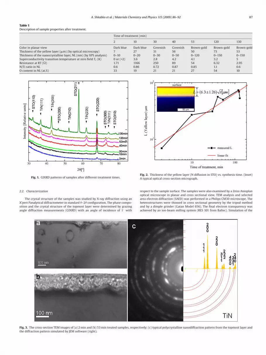
A. Shkabko et al. / Materials Chemistry and Physics 115 (2009) 86–92 87
Table 1Description of sample properties after treatment.
Time of treatment (min)
2 10 30 40 53 120 130
Color in planar view Dark blue Dark blue Greenish Greenish Brown-gold Brown-gold Brown-goldThickness of the yellow layer (�m) (by optical microscopy) 7 27 31 56 50 73 53Thickness of the nanocrystalline layer, NL (nm) (by XPS analysis) 0–10 0–20 0–30 0–50 0–120 0–150 0–150Superconductivity transition temperature at zero field Tc (K) 0 or (<2) 3.6 2.8 4.2 4.1 3.2 5Resistance at RT (�) 1.71 1166 250 89 54 6.32 2.95N/Ti ratio in NL 0.6 0.86 0.72 0.87 0.85 1.1 0.6O content in NL (at.%) 33 19 21 21 27 54 10
2
Xsa
Ft
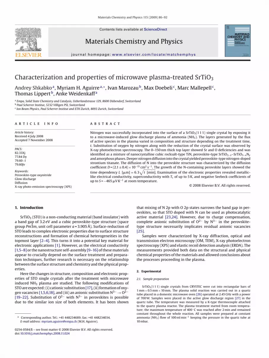
Fig. 1. GIXRD patterns of samples after different treatment times.
.2. Characterization
The crystal structure of the samples was studied by X-ray diffraction using an’pert Panalytical diffractometer in standard �–2� configuration. The phase compo-ition and the crystal structure of the topmost layer were determined by grazingngle diffraction measurements (GIXRD) with an angle of incidence of 1◦ with
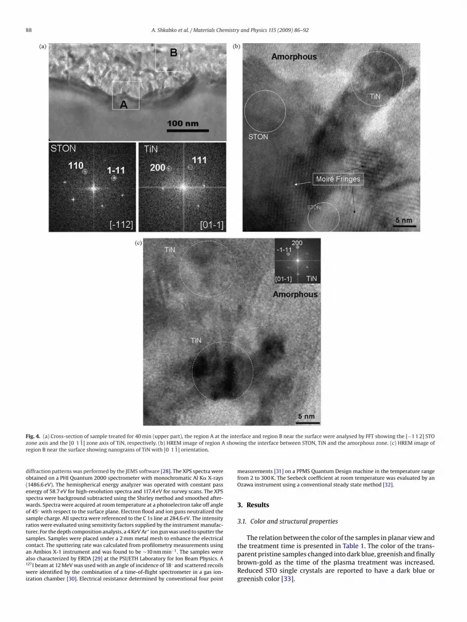
ig. 3. The cross-section TEM images of (a) 2 min and (b) 53 min treated samples, respecthe diffraction pattern simulated by JEM software (right).
Fig. 2. Thickness of the yellow layer (N diffusion in STO) vs. synthesis time. (Inset)A typical optical cross-section micrograph.
respect to the sample surface. The samples were also examined by a Zeiss Axioplan
optical microscope in planar and cross sectional view. TEM analysis and selectedarea electron diffraction (SAED) was performed in a Philips CM30 microscope. Theheterostructures were thinned in cross sectional geometry by the tripod methodand by a dimple grinder (Gatan Model 656). The final electron transparency wasachieved by an ion-beam milling system (RES 101 from Baltec). Simulation of theively; (c) typical polycrystalline nanodiffraction pattern from the topmost layer and
88 A. Shkabko et al. / Materials Chemistry and Physics 115 (2009) 86–92
F e intez showr
do(eswosrtscaa1
wi
ig. 4. (a) Cross-section of sample treated for 40 min (upper part), the region A at thone axis and the [0 1 1̄] zone axis of TiN, respectively. (b) HREM image of region Aegion B near the surface showing nanograins of TiN with [0 1 1̄] orientation.
iffraction patterns was performed by the JEMS software [28]. The XPS spectra werebtained on a PHI Quantum 2000 spectrometer with monochromatic Al K� X-rays1486.6 eV). The hemispherical energy analyzer was operated with constant passnergy of 58.7 eV for high-resolution spectra and 117.4 eV for survey scans. The XPSpectra were background subtracted using the Shirley method and smoothed after-ards. Spectra were acquired at room temperature at a photoelectron take off anglef 45◦ with respect to the surface plane. Electron flood and ion guns neutralized theample charge. All spectra were referenced to the C 1s line at 284.6 eV. The intensityatios were evaluated using sensitivity factors supplied by the instrument manufac-urer. For the depth composition analysis, a 4 KeV Ar+ ion gun was used to sputter theamples. Samples were placed under a 2 mm metal mesh to enhance the electrical
ontact. The sputtering rate was calculated from profilometry measurements usingn Ambios X-1 instrument and was found to be ∼10 nm min−1. The samples werelso characterized by ERDA [29] at the PSI/ETH Laboratory for Ion Beam Physics. A27I beam at 12 MeV was used with an angle of incidence of 18◦ and scattered recoilsere identified by the combination of a time-of-flight spectrometer in a gas ion-zation chamber [30]. Electrical resistance determined by conventional four point
rface and region B near the surface were analysed by FFT showing the [−1 1 2] STOing the interface between STON, TiN and the amorphous zone. (c) HREM image of
measurements [31] on a PPMS Quantum Design machine in the temperature rangefrom 2 to 300 K. The Seebeck coefficient at room temperature was evaluated by anOzawa instrument using a conventional steady state method [32].
3. Results
3.1. Color and structural properties
The relation between the color of the samples in planar view and
the treatment time is presented in Table 1. The color of the trans-parent pristine samples changed into dark blue, greenish and finallybrown-gold as the time of the plasma treatment was increased.Reduced STO single crystals are reported to have a dark blue orgreenish color [33].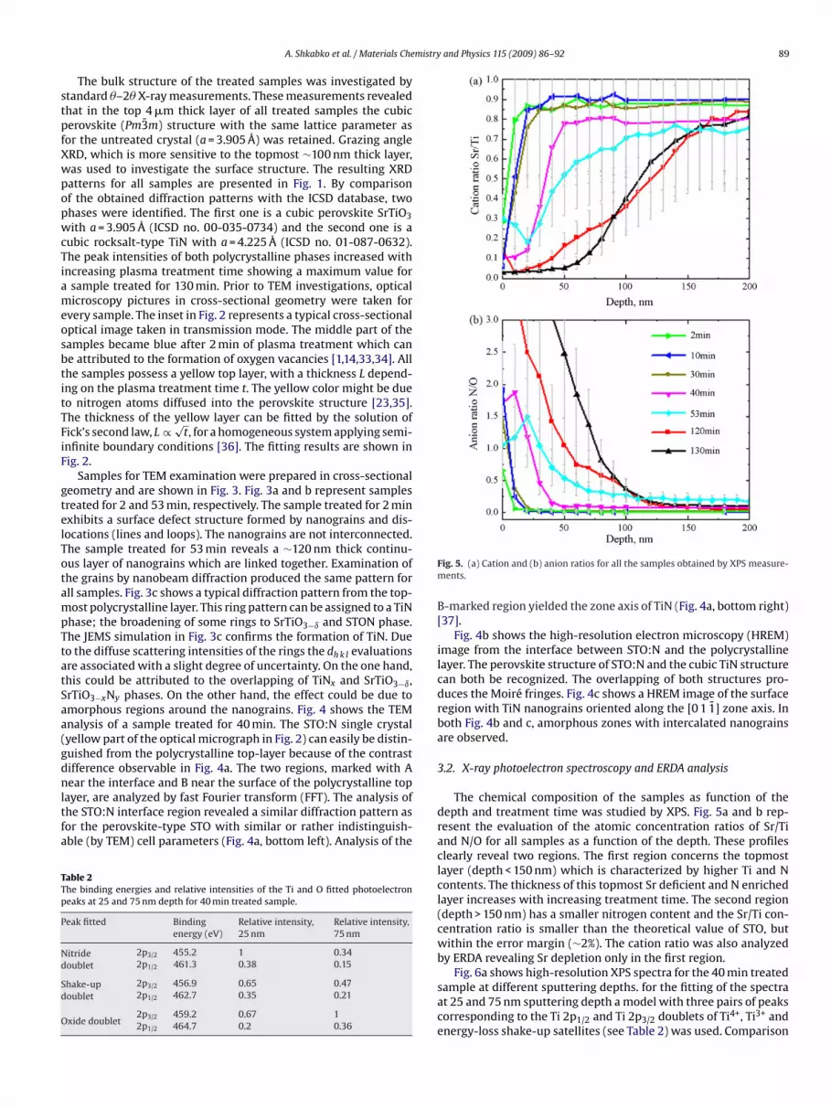
mistry and Physics 115 (2009) 86–92 89
stpfXwpopwcTiameosbtitTFiF
gtelTotampTtatSaa(gdnltfa
TTp
P
Nd
Sd
O
A. Shkabko et al. / Materials Che
The bulk structure of the treated samples was investigated bytandard �–2� X-ray measurements. These measurements revealedhat in the top 4 �m thick layer of all treated samples the cubicerovskite (Pm3̄m) structure with the same lattice parameter asor the untreated crystal (a = 3.905 Å) was retained. Grazing angleRD, which is more sensitive to the topmost ∼100 nm thick layer,as used to investigate the surface structure. The resulting XRDatterns for all samples are presented in Fig. 1. By comparisonf the obtained diffraction patterns with the ICSD database, twohases were identified. The first one is a cubic perovskite SrTiO3ith a = 3.905 Å (ICSD no. 00-035-0734) and the second one is a
ubic rocksalt-type TiN with a = 4.225 Å (ICSD no. 01-087-0632).he peak intensities of both polycrystalline phases increased withncreasing plasma treatment time showing a maximum value for
sample treated for 130 min. Prior to TEM investigations, opticalicroscopy pictures in cross-sectional geometry were taken for
very sample. The inset in Fig. 2 represents a typical cross-sectionalptical image taken in transmission mode. The middle part of theamples became blue after 2 min of plasma treatment which cane attributed to the formation of oxygen vacancies [1,14,33,34]. Allhe samples possess a yellow top layer, with a thickness L depend-ng on the plasma treatment time t. The yellow color might be dueo nitrogen atoms diffused into the perovskite structure [23,35].he thickness of the yellow layer can be fitted by the solution ofick’s second law, L ∝ √
t, for a homogeneous system applying semi-nfinite boundary conditions [36]. The fitting results are shown inig. 2.
Samples for TEM examination were prepared in cross-sectionaleometry and are shown in Fig. 3. Fig. 3a and b represent samplesreated for 2 and 53 min, respectively. The sample treated for 2 minxhibits a surface defect structure formed by nanograins and dis-ocations (lines and loops). The nanograins are not interconnected.he sample treated for 53 min reveals a ∼120 nm thick continu-us layer of nanograins which are linked together. Examination ofhe grains by nanobeam diffraction produced the same pattern forll samples. Fig. 3c shows a typical diffraction pattern from the top-ost polycrystalline layer. This ring pattern can be assigned to a TiN
hase; the broadening of some rings to SrTiO3−ı and STON phase.he JEMS simulation in Fig. 3c confirms the formation of TiN. Dueo the diffuse scattering intensities of the rings the dh k l evaluationsre associated with a slight degree of uncertainty. On the one hand,his could be attributed to the overlapping of TiNx and SrTiO3−ı,rTiO3−xNy phases. On the other hand, the effect could be due tomorphous regions around the nanograins. Fig. 4 shows the TEMnalysis of a sample treated for 40 min. The STO:N single crystalyellow part of the optical micrograph in Fig. 2) can easily be distin-uished from the polycrystalline top-layer because of the contrastifference observable in Fig. 4a. The two regions, marked with Aear the interface and B near the surface of the polycrystalline top
ayer, are analyzed by fast Fourier transform (FFT). The analysis ofhe STO:N interface region revealed a similar diffraction pattern asor the perovskite-type STO with similar or rather indistinguish-ble (by TEM) cell parameters (Fig. 4a, bottom left). Analysis of the
able 2he binding energies and relative intensities of the Ti and O fitted photoelectroneaks at 25 and 75 nm depth for 40 min treated sample.
eak fitted Bindingenergy (eV)
Relative intensity,25 nm
Relative intensity,75 nm
itrideoublet
2p3/2 455.2 1 0.342p1/2 461.3 0.38 0.15
hake-upoublet
2p3/2 456.9 0.65 0.472p1/2 462.7 0.35 0.21
xide doublet2p3/2 459.2 0.67 12p1/2 464.7 0.2 0.36
Fig. 5. (a) Cation and (b) anion ratios for all the samples obtained by XPS measure-ments.
B-marked region yielded the zone axis of TiN (Fig. 4a, bottom right)[37].
Fig. 4b shows the high-resolution electron microscopy (HREM)image from the interface between STO:N and the polycrystallinelayer. The perovskite structure of STO:N and the cubic TiN structurecan both be recognized. The overlapping of both structures pro-duces the Moiré fringes. Fig. 4c shows a HREM image of the surfaceregion with TiN nanograins oriented along the [0 1 1̄] zone axis. Inboth Fig. 4b and c, amorphous zones with intercalated nanograinsare observed.
3.2. X-ray photoelectron spectroscopy and ERDA analysis
The chemical composition of the samples as function of thedepth and treatment time was studied by XPS. Fig. 5a and b rep-resent the evaluation of the atomic concentration ratios of Sr/Tiand N/O for all samples as a function of the depth. These profilesclearly reveal two regions. The first region concerns the topmostlayer (depth < 150 nm) which is characterized by higher Ti and Ncontents. The thickness of this topmost Sr deficient and N enrichedlayer increases with increasing treatment time. The second region(depth > 150 nm) has a smaller nitrogen content and the Sr/Ti con-centration ratio is smaller than the theoretical value of STO, butwithin the error margin (∼2%). The cation ratio was also analyzedby ERDA revealing Sr depletion only in the first region.
Fig. 6a shows high-resolution XPS spectra for the 40 min treatedsample at different sputtering depths. for the fitting of the spectraat 25 and 75 nm sputtering depth a model with three pairs of peakscorresponding to the Ti 2p1/2 and Ti 2p3/2 doublets of Ti4+, Ti3+ andenergy-loss shake-up satellites (see Table 2) was used. Comparison

90 A. Shkabko et al. / Materials Chemistry and Physics 115 (2009) 86–92
Fig. 6. (a) Reconstruction of the Ti 2p chemical shift during XPS depth profile anal-ysis; (b and c) deconvolution of the Ti 2p peaks 75 and 25 nm, respectively.
Fig. 7. Nitrogen concentration vs. depth for 130 min treated sample based on exper-imental XPS data. (Inset) Linear fit in the depth range of 0.2–0.8 �m.
of the spectra demonstrates that Ti is present in different chemi-cal states in the two regions (Fig. 6b and c). The spectrum at 25 nmdepth is typical for the first region and the spectrum at 75 nm depthis typical for the second region. The Ti 2p spectrum obtained for the
first region is shifted to lower binding energies confirming prefer-ential formation of Ti3+–N bonds on the surface, while the spectrumfor the second region corresponds to the peak positions typical forTi4+ [38–41].Fig. 8. (a) Temperature dependence of the resistances for plasma-treated samples,(b) enlarged low-temperature region showing the superconductivity transition for120 and 130 min treated samples.
mistry
s(ScdtiIwfiDl
3
aFRfthTtatTsoSS
4
poypfOtadtyttqD
pTgihrhsIsasi
[[[
[
[[[[
A. Shkabko et al. / Materials Che
XPS composition analysis reveals maximum N content in theample treated for 130 min (Fig. 7). The high-nitrogen content∼35 at.%) was found in the topmost surface layer, which is stronglyr-depleted (3 at.%) and enriched with Ti (53 at.%). The nitrogen con-entration decreases gradually from 35% to 3.5% with increasingepth (0–150 nm), while the Sr content increases and the Ti con-ent decreases simultaneously. The Sr content reaches ∼20%, whichs consistent with the cation stoichiometric composition of SrTiO3.n the range of 200–800 nm the nitrogen content decreases linearly
ith depth (inset Fig. 7). In this deep region, the diffusion coef-cient for the diffusion of nitrogen into the perovskite lattice of= (2.1 ± 0.4) × 10−15 cm2 s−1 was calculated applying Fick’s second
aw.
.3. Electrical and thermoelectrical properties
Fig. 8a shows the electrical resistivity of the treated sampless a function of temperature. The sample treated for 2 min (seeig. 3a), shows metallic behavior with a residual resistance ratio(300 K)/R(4.2 K) of ∼103 which is similar to the values obtainedor reduced STO crystals [5,8]. The samples with longer treatmentimes exhibited superconductivity with Tc < 5 K and considerablyigher resistances (up to the k� range) at temperatures above Tc.he superconducting transition temperature also depends on thereatment procedure (Table 1). The maximum transition temper-ture measured in zero magnetic field reaches 5 K, which is closeo the value of Tc = 5.6 K for TiN [42] and higher than the values ofc max = 0.3 K for reduced STO [43]. The Seebeck coefficients of thetudied samples are S ∼ −400 �V K−1 at about 300 K which is tworders of magnitude higher than the reported data for TiN with= −7.8 �V K−1 [44], but lower compared to the values for reducedTO with S = −890 �V K−1 [45].
. Discussions and conclusions
Plasma ammonolysis of SrTiO3 single crystals in a microwavelasma partially replace O2− by N3− resulting in the formationf layers with different compositions and structures. The anal-sis by GIXRD, TEM, XPS and ERDA shows that the microwavelasma treatment results in modifications of the topmost sur-
ace layer (0–150 nm) are accompanied by depletion in Sr andatoms. In this region nanocrystalline grains of cubic rocksalt-
ype TiN were formed together with perovskite-type STO:N andmorphous material. Deeper layers (L ≥ 150 nm) had a yellow colorue to the formation of N-doped STO and revealed single crys-al perovskite-type structure. The thickness of this N-doped STOellow layer increases with increasing treatment time and was fit-ed with Fick’s second law, resulting in the time relationship forhe diffusion length of L [�m] = 6.3
√t [min]. XPS depth profile
uantification of the N diffusion into STO yields a coefficient of= (2.1 ± 0.4) × 10−15 cm2 s−1.
The formation of this layered structure is attributable to theroperties of the microwave plasma used for the sample treatment.he plasma treatment results in the decomposition of flowing NH3as by microwave radiation and produces an active species fluxn the discharge region [27] comprising active species of nitrogen,ydrogen and electrons. The electron energy in the glow dischargeegion is about 10–100 eV [25] which is 3 orders of magnitudeigher than those for atoms/ions. The active species damage theample surface causing loss of Sr and O from the surface of SrTiO3.
n ion sputtering [14] and PLD thin film growth [46] experiments,imilar Sr and O losses were observed. Moreover, after thermalnnealing, the formation of Sr and O vacancies have energeticallyimilar probability [47]. The formation of TiN or amorphous phasesn the topmost layer, can also be related to an excess of nitrogen at[[
[
and Physics 115 (2009) 86–92 91
the surface. A comparable effect of degradation was observed in N-doped SrTiO3 films produced by reactive RF magnetron sputteringin a Ar–N2 mixture [35].
Apart from the content of active species, the NH3 plasma also hasreductive properties, leading to a reduction of the crystal surfaceand thus to the formation of new phases.
The diffusion of nitrogen into the perovskite structureat the maximum temperature of 400 ◦C applied during theplasma treatments is characterized by a diffusion coefficient ofD = (2.1 ± 0.4) × 10−15 cm2 s−1.
The results of the electrical measurements of the treated sam-ples also varied with the length of the treatment. For the sampletreated for 2 min, where the formed TiN nanograins at the surfacewere yet not linked together, the value of the electrical conductivitywas in the range characteristic for metals. An increase of the treat-ment time yielded samples with interconnected TiN nanograins atthe surface. These samples exhibited much higher resistivities, butalso showed superconductivity with different Tc (<5 K). The sam-ple treated for 2 min showed a metallic behavior, very similar toreduced STO. The incorporation of a small amount of nitrogen intoSTO single crystal has minor influence on the transport proper-ties. Samples treated for a longer time reveal a surface layer ofmixed phases, i.e. TiNx, SrTiO3−xNy, SrTiO3−ı (in interconnectednanograins, Fig. 3b). The superconductivity with transition tem-peratures depending on the processing time (Fig. 8 inset) couldbe assigned to the presence of a TiNx related phase. The transitiontemperature in TiNx depends on the Ti/N content, reaching a maxi-mum Tc = 5.6 K for Ti/N = 1. Small deviations from the stoichiometriccomposition affect the transition temperature.
On the other hand the samples reveal a large negative See-beck coefficient S = −465 �V K−1 at room temperature, which is twoorders of magnitude higher than for TiN and comparable to reducedSTO.
Acknowledgments
The authors thank to D. Logfdvinovich, R. Hauert for discussionand support. The work was supported by Swiss National ScienceFoundation and by the NCCR MaNEP.
References
[1] D. Kan, R. Kanda, Y. Kanemitsu, Y. Shimakawa, M. Takano, T. Terashima, A.Ishizumi, Appl. Phys. Lett. 88 (19) (2006) 816.
[2] K. Szot, W. Speier, Phys. Rev. B 60 (8) (1999) 5909.[3] C. Sabathier, J. Chaumont, S. Rouziere, A. Traverse, Nucl. Instrum. Meth. B 234
(4) (2005) 509.[4] K. Szot, M. Pawelczyk, J. Herion, C. Freiburg, J. Albers, R. Waser, J. Hulliger, J.
Kwapulinski, J. Dec, Appl. Phys. A 62 (4) (1996) 335.[5] D.W. Reagor, V.Y. Butko, Nat. Mater. 4 (8) (2005) 593.[6] D.H. Choi, D. Lee, H. Sim, M. Chang, H.S. Hwang, Appl. Phys. Lett. 88 (8) (2006)
082904.[7] M. Jourdan, N. Blumer, H. Adrian, Eur. Phys. J. B 33 (1) (2003) 25.[8] K.S. Takahashi, D. Matthey, D. Jaccard, J.M. Triscone, Ann. Phys.-Berlin 13 (1–2)
(2004) 68.[9] T. Kubo, H. Nozoye, Surf. Sci. 542 (3) (2003) 177.10] D.S. Deak, F. Silly, D.T. Newell, M.R. Castell, J. Phys. Chem. B 110 (18) (2006) 9246.11] N. Erdman, L.D. Marks, Surf. Sci. 526 (1–2) (2003) 107.12] N. Erdman, K.R. Poeppelmeier, M. Asta, O. Warschkow, D.E. Ellis, L.D. Marks,
Nature 419 (6902) (2002) 55.13] A. Gunhold, K. Gomann, L. Beuermann, V. Kempter, G. Borchardt, W. Maus-
Friedrichs, Surf. Sci. 566 (2004) 105.14] V.E. Henrich, G. Dresselhaus, H.J. Zeiger, Phys. Rev. B 17 (12) (1978) 4908.15] K. Johnston, M.R. Castell, A.T. Paxton, M.W. Finnis, Phys. Rev. B 70 (8.) (2004).16] F. Silly, D.T. Newell, M.R. Castell, Surf. Sci. 600 (17) (2006) L219.17] T.K.Y. Wong, B.J. Kennedy, C.J. Howard, B.A. Hunter, T. Vogt, J. Sol. Stat. Chem.
156 (2) (2001) 255.18] K. Szot, W. Speier, G. Bihlmayer, R. Waser, Nat. Mater. 5 (4) (2006) 312.19] R. Aguiar, A. Weidenkaff, C.W. Schneider, A. Reller, S.G. Ebbinghaus, Prog. Sol.
Stat. Chem. 35 (2–4) (2007) 291.20] D. Logvinovich, A. Borger, M. Dobeli, S.G. Ebbinghaus, A. Reller, A. Weidenkaff,
Prog. Sol. Stat. Chem. 35 (2–4) (2007) 281.
9 mistry
[
[
[[
[
[[[[
[
[
[
[
[
[
[
[
[
[
[
[[
[
2 A. Shkabko et al. / Materials Che
21] I. Marozau, M. Döbeli, T. Lippert, D. Logvinovich, M. Mallepell, A. Shkabko, A.Weidenkaff, A. Wokaun, Appl. Phys. A 89 (2) (2007) 933.
22] D. Logvinovich, R. Aguiar, R. Robert, M. Trottman, S.G. Ebbinghaus, A. Reller, A.Weidenkaff, J. Sol. Stat. Chem. (2007).
23] M. Miyauchi, M. Takashio, H. Tobimatsu, Langmuir 20 (1) (2004) 232.24] Y.Y. Mi, S.J. Wang, J.W. Chai, J.S. Pan, C.H.A. Huan, Y.P. Feng, C.K. Ong, Appl. Phys.
Lett. 89 (23) (2006) 2119221.25] J.H. Moore, Encyclopedia of Chemical Physics and Physical Chemistry, Institute
of Physics, Bristol, 2001.26] D.J. Brooks, R.E. Douthwaite, Rev. Sci. Instrum. 75 (12) (2004) 5277.27] M. Moisan, Microwave Excited Plasmas, Elsevier, Amsterdam, 1992.28] P.A. Stadelmann, Ultramicroscopy 21 (2) (1987) 131.29] J. Tirira, Y. Serruys, P. Trocellier, Forward Recoil Spectrometry Applications to
Hydrogen Determination in Solids, Plenum, New York, 1996.30] C. Kottler, M. Dobeli, F. Glaus, M. Suter, Nucl. Instrum. Meth. B 248 (1) (2006)
155.31] D.K. Schroder, Semiconductor Material and Device Characterization, John Wiley,
Hoboken, NJ, 2006.32] D.M. Rowe, Thermoelectrics Handbook Macro to Nano, Taylor & Francis, Boca
Raton, 2006.33] D.S. Kan, T. Terashima, R. Kanda, A. Masuno, K. Tanaka, S.C. Chu, H. Kan, A.
Ishizumi, Y. Kanemitsu, Y. Shimakawa, M. Takano, Nat. Mater. 4 (11) (2005) 816.34] M.A. Alario-Franco, M. Vallet-Regi, Nature 270 (5639) (1977) 706.
[
[[
[
and Physics 115 (2009) 86–92
35] X.F. Chen, H. Lu, H.J. Bian, W.G. Zhu, C.Q. Sun, O.K. Tan, J. Electroceram. 16 (4)(2006) 419.
36] J. Philibert, S.J. Rothman, Atom Movement Diffusion and Mass Transport inSolids, Les Editions de Physique, Les Ulis, 1991.
37] M.A. Lieberman, A.J. Lichtenberg, Principles of Plasma Discharges and MaterialsProcessing, Wiley, Hoboken, 2005.
38] J. Guillot, J.M. Chappe, O. Heintz, N. Martin, L. Imhoff, J. Takadoum, Acta Mater.54 (11) (2006) 3067.
39] K.J. Kim, D.W. Moon, S.H. Nam, W.J. Lee, H.G. Kim, Surf. Interf. Anal. 23 (13)(1995) 851.
40] I. Milosev, H.H. Strehblow, B. Navinsek, M. Metikoshukovic, Surf. Interf. Anal. 23(7–8) (1995) 529.
41] I.L. Strydom, S. Hofmann, J. Electron Spectrosc. 56 (2) (1991) 85.42] L.E. Toth, Transition Metal Carbides and Nitrides, Academic Press, New York,
1971.43] C.S. Koonce, M.L. Cohen, J.F. Schooley, W.R. Hosler, E.R. Pfeiffer, Phys. Rev. 163
(2) (1967) 380.
44] G.V. Samsonov, T.S. Verkhogliadova, Doklady Akademii Nauk SSSR 142 (3)(1962) 608.45] H.P.R. Frederikse, W.R. Thurber, W.R. Hosler, Phys. Rev. A 134 (2A) (1964) A442.46] T. Ohnishi, M. Lippmaa, T. Yamamoto, S. Meguro, H. Koinuma, Appl. Phys. Lett.
87 (24) (2005) 2419191.47] R. Meyer, R. Waser, J. Helmbold, G. Borchardt, J. Electroceram. 9 (2) (2002) 103.


