Embed Size (px)
Citation preview
MODULES, SYSTEMS, AND APPLICATIONSIN THERMOELECTRICS“The selection of topics of comprehensive and thorough, covering topics all the way from recent developments in new materials such as polymer thermoelectrics to module scale design for solar thermal applications … The writing is clear and thorough, and written at a suitable level for those learning the field, while still containing advanced topics for members of the thermoelectric community. … many recent developments in the field into one refer-ence. … essential and comprehensive reference for researchers in thermoelectrics as well as for those needing a general overview of this growing field. ... a timely update, covering many recent developments in the field and incorporating topics important for commercialization efforts.”—Austin Minnich, California Institute of Technology, Pasadena, USA
Modules, Systems, and Applications in Thermoelectrics examines current interest in alternative energy and energy harvesting, specifically, the current efforts to use thermoelectric generators (TGs) to reduce emissions and save fuel.
Features:
• Focuses on the international efforts to reduce carbon emissions by using thermoelectrics in automobile exhaust heat recovery
• Discusses the practical, novel, and truly groundbreaking applications of thermoelectrics in a range of markets, including the U.S., Europe, Japan, Korea, and India
• Includes updated theoretical considerations that provide an insight into scientific and commercially profitable avenues of research
• Explores the latest activities in thermoelectrics and their application in energy harvesting and in reducing global warming
The book expounds on the strong interest in Japan, Korea, and Europe to incorporate TGs in cars to reduce fuel consumption and meet EU carbon dioxide emission targets; the European plans to build an isotopic powered thermoelectric generator; and India’s use of TGs in converting hot water from steel mills into electricity.
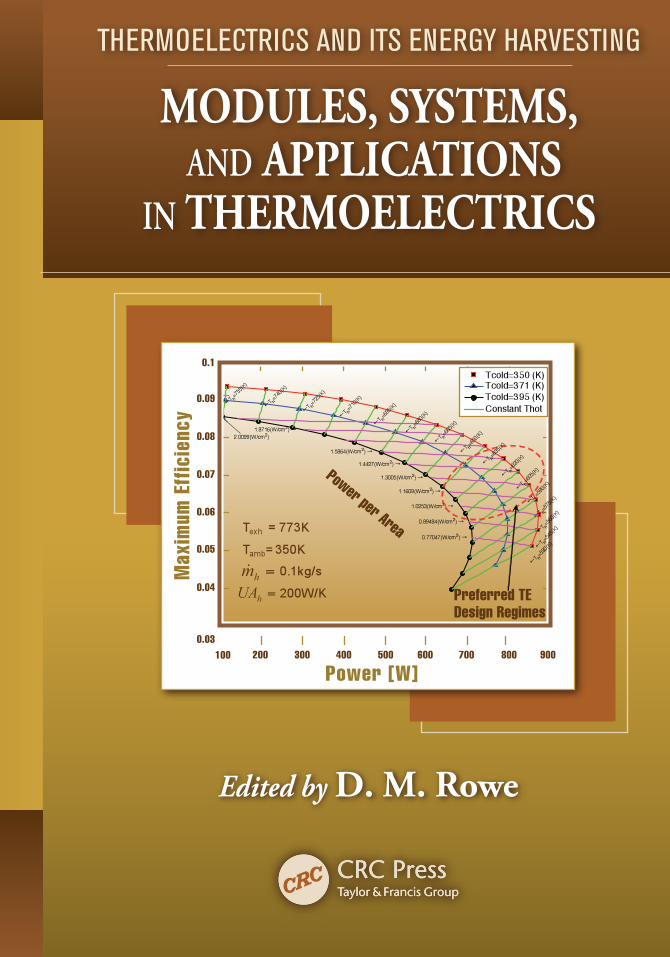
Power [W]
Max
imum
Eff
icie
ncy
0.09
0.08
0.07
0.06
0.05
0.04
0.03100 200 300 400 500 600 700 800 900
0.1
Preferred TEDesign Regimes
Power per Area
Rowe
K13465
ISBN: 978-1-4398-7472-1
9 781439 874721
90000
Edited by D. M. Rowe
THERMOELECTRICS AND ITS ENERGY HARVESTINGMODULES, SYSTEMS, AND APPLICATIONS
IN THERMOELECTRICS
THERMOELECTRICS AND ITS ENERGY HARVESTING
THERMOELECTRICS AND ITS ENERGY HARVESTING
MO
DU
LES, SYSTEMS, AND APPLICATIO
NS IN TH
ERMO
ELECTRICS
THERMOELECTRICS AND ITS ENERGY HARVESTING
MODULES, SYSTEMS, AND APPLICATIONS
IN THERMOELECTRICS

CRC Press is an imprint of theTaylor & Francis Group, an informa business
Boca Raton London New York
THERMOELECTRICS AND ITS ENERGY HARVESTING
MODULES, SYSTEMS, AND APPLICATIONS
IN THERMOELECTRICS
Edited by D. M. RoweOBE, DSc, PhD
MATLAB® and Simulink® are trademarks of The MathWorks, Inc. and are used with permission. The MathWorks does not war-rant the accuracy of the text or exercises in this book. This book’s use or discussion of MATLAB® and Simulink® software or related products does not constitute endorsement or sponsorship by The MathWorks of a particular pedagogical approach or particular use of the MATLAB® and Simulink® software.
CRC PressTaylor & Francis Group6000 Broken Sound Parkway NW, Suite 300Boca Raton, FL 33487-2742
© 2012 by Taylor & Francis Group, LLCCRC Press is an imprint of Taylor & Francis Group, an Informa business
No claim to original U.S. Government worksVersion Date: 20120511
International Standard Book Number-13: 978-1-4665-6030-7 (eBook - PDF)
This book contains information obtained from authentic and highly regarded sources. Reasonable efforts have been made to publish reliable data and information, but the author and publisher cannot assume responsibility for the validity of all materials or the consequences of their use. The authors and publishers have attempted to trace the copyright holders of all material repro-duced in this publication and apologize to copyright holders if permission to publish in this form has not been obtained. If any copyright material has not been acknowledged please write and let us know so we may rectify in any future reprint.
Except as permitted under U.S. Copyright Law, no part of this book may be reprinted, reproduced, transmitted, or utilized in any form by any electronic, mechanical, or other means, now known or hereafter invented, including photocopying, microfilming, and recording, or in any information storage or retrieval system, without written permission from the publishers.
For permission to photocopy or use material electronically from this work, please access www.copyright.com (http://www.copy-right.com/) or contact the Copyright Clearance Center, Inc. (CCC), 222 Rosewood Drive, Danvers, MA 01923, 978-750-8400. CCC is a not-for-profit organization that provides licenses and registration for a variety of users. For organizations that have been granted a photocopy license by the CCC, a separate system of payment has been arranged.
Trademark Notice: Product or corporate names may be trademarks or registered trademarks, and are used only for identifica-tion and explanation without intent to infringe.
Visit the Taylor & Francis Web site athttp://www.taylorandfrancis.com
and the CRC Press Web site athttp://www.crcpress.com
v
Contents
Preface....................................................................................................................... ix
Editor ........................................................................................................................ xi
Contributors .......................................................................................................... xiii
SECTION I Thermoelectric Materials and Properties
1 Nanostructured Thermoelectric Materials ................................................... 1-1Zhifeng Ren, Gang Chen, and Mildred Dresselhaus
2 Design and Realization of Nanostructured Inorganic Intergrowths ...........2-1M. Beekman, C. Heideman, M. Anderson, M. Smeller, R. Atkins, Q. Lin, N. Nguyen, and D.C. Johnson
3 Bulk Nanocomposites of Thermoelectric Materials .....................................3-1Lidong Chen, Zhen Xiong, Ruiheng Liu, and Wenqing Zhang
4 Layer-Structured Metal Sulfides as Novel Thermoelectric Materials ..........4-1C.L. Wan, Y.F. Wang, N. Wang, Y.E. Putri, W. Norimatsu, M. Kusunoki, and K. Koumoto
5 Thermoelectric Properties of Quantum Wires within Chrysotile Asbestos Nanotubes .......................................................................................5-1M.V. Vedernikov, Y.V. Ivanov, O.N. Uryupin, and Y.A. Kumzerov
6 Bismuth Telluride Alloys for Waste Energy Harvesting and Cooling Applications .....................................................................................6-1H. Scherrer and S. Scherrer
7 Optimization of Solid Solutions Based on Bismuth and Antimony Chalcogenides above Room Temperature...................................................... 7-1L.N. Lukyanova, V.A. Kutasov, P.P. Konstantinov, and V.V. Popov
8 Effect of Vacancy Distribution on the Thermoelectric Properties of Gallium and Indium Chalcogenides .........................................................8-1Ken Kurosaki and Shinsuke Yamanaka
9 Thermoelectric Inverse Clathrates ................................................................9-1Matthias Falmbigl and Peter F. Rogl
vi Contents
10 Recent Advances in the Development of Efficient N-Type Skutterudites ... 10-1Ctirad Uher
11 Silicide Thermoelectrics: State of the Art and Prospects ........................... 11-1M.I. Fedorov and V.K. Zaitsev
12 Thermoelectric Properties of Intermetallic Hybridization Gap and Pseudo-Gap Systems: Fe2VAl and CoSi ................................................ 12-1Donald T. Morelli
13 Novel Power Factor of Si–Ge System ...........................................................13-1Yoichi Okamoto and Hiroaki Takiguchi
14 Boride Thermoelectrics: High-Temperature Thermoelectric Materials..... 14-1Takao Mori
15 Polymer Thermoelectric Materials ..............................................................15-1Yoshikazu Shinohara
16 Thermomechanical Properties of Thermoelectric Materials ..................... 16-1E.D. Case
SECTION II Thermoelectric Modules, Devices, and Applications
17 Miniaturized Thermoelectric Converters, Technologies, and Applications .......................................................................................... 17-1Harald Böttner and Joachim Nurnus
18 Application of Thermoelectrics for Thermal Management of High-Power Microelectronics .................................................................. 18-1Vladimir A. Semenyuk
19 Millikelvin Tunnelling Refrigerators .......................................................... 19-1M.J. Prest, T.E. Whall, E.H.C. Parker, and D.R. Leadley
20 Heat Dissipaters ............................................................................................20-1Jesus Esarte, Cecilia Wolluschek, Jesus Ma Blanco, and David Prieto
21 Thin-Film Superlattice Thermoelectric Devices for Energy Harvesting and Thermal Management ........................................................................... 21-1Rama Venkatasubra manian, Jonathan Pierce, �omas Colpitts, Gary Bulman, David Stokes, John Posthill, Phil Barletta, David Koester, Brooks O’Quinn, and Edward Siivola
SECTION III Thermoelectric Systems and Applications
22 Thermoelectric Energy Recovery Systems: Thermal, Thermoelectric, and Structural Considerations .....................................................................22-1Terry J. Hendricks and Douglas T. Crane
viiContents
23 Thermoelectric Harvesting of Low-Temperature Heat ...............................23-1David Michael Rowe
24 Solar Thermoelectric Power Conversion .....................................................24-1Daniel Kraemer, Kenneth McEnaney, Zhifeng Ren, and Gang Chen
25 Automotive Applications of Thermoelectric Materials ..............................25-1Jihui Yang and Francis R. Stabler
26 Medical Applications of Thermoelectrics ...................................................26-1Alic Chen and Paul K. Wright

ix
Preface
Nanotechnology has had a profound positive impact on thermoelectrics. It has contributed substantially to the development of advanced materials with improved thermoelectric and physical properties. �is in turn has resulted in signi�cantly increasing the economic competitiveness of thermoelectric energy harvesting.
�e Handbook, Modules, Systems, and Applications in �ermoelectrics is comprised of 26 chapters by 75 contributors who are leading experts in their respective �elds. As in previous CRC �ermoelectric Handbooks, the majority of chapters are reviews. �e book is divided into three sections. Section I deals with �ermoelectric Materials and Properties. Section II discusses �ermoelectric Modules, Devices, and Applications, and Section III explains �ermoelectric Systems and Applications.
Section I is the largest, comprising 16 chapters, with the �rst chapter “Nanostructured �ermoelectric Materials,” by Ren, Chen, and Dresselhaus, setting the scene for this all embracing materials section. �e �ve chapters of Section II provide a comprehensive overview of progress made in the development of modules and their application in devices. Highlighted is the dramatic progress made in device minia-turization and its successful commercialization in energy harvesting. Section III, also comprised of �ve chapters, is devoted to thermoelectric energy harvesting and contains comprehensive reviews of the solar, automotive, and medical harvesting of waste heat.
Again, I have tried to preserve the international ¡avor of previous Handbooks and made minor changes only where necessary to clarify the meaning. �e compilation of the two volume set, �ermo-electrics and Its Energy Harvesting, has been made possible by authoritative contributions from fellow thermoelectricians. �e thermoelectric fraternity is deeply indebted to these authors who have unself-ishly devoted their time to this project.
Finally, I am thankful to my wife Barbara, whose help has enabled me to bring this labor of love to a successful conclusion.
MATLAB• is a registered trademark of �e MathWorks, Inc. For product information, please contact:
�e MathWorks, Inc.3 Apple Hill DriveNatick, MA 01760-2098, USATel: 508-647-7000Fax: 508-647-7001E-mail: [email protected]: www.mathworks.com

xi
Editor
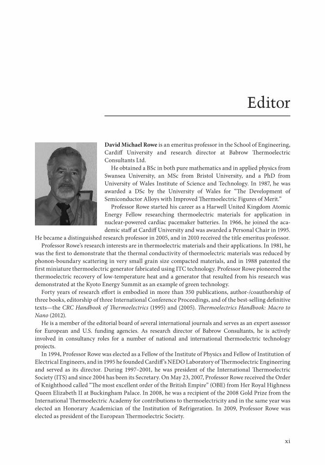
David Michael Rowe is an emeritus professor in the School of Engineering, Cardi¤ University and research director at Babrow �ermoelectric Consultants Ltd.
He obtained a BSc in both pure mathematics and in applied physics from Swansea University, an MSc from Bristol University, and a PhD from University of Wales Institute of Science and Technology. In 1987, he was awarded a DSc by the University of Wales for “�e Development of Semiconductor Alloys with Improved �ermoelectric Figures of Merit.”
Professor Rowe started his career as a Harwell United Kingdom Atomic Energy Fellow researching thermoelectric materials for application in nuclear-powered cardiac pacemaker batteries. In 1966, he joined the aca-demic sta¤ at Cardi¤ University and was awarded a Personal Chair in 1995.
He became a distinguished research professor in 2005, and in 2010 received the title emeritus professor.Professor Rowe’s research interests are in thermoelectric materials and their applications. In 1981, he
was the �rst to demonstrate that the thermal conductivity of thermoelectric materials was reduced by phonon-boundary scattering in very small grain size compacted materials, and in 1988 patented the �rst miniature thermoelectric generator fabricated using ITC technology. Professor Rowe pioneered the thermoelectric recovery of low-temperature heat and a generator that resulted from his research was demonstrated at the Kyoto Energy Summit as an example of green technology.
Forty years of research e¤ort is embodied in more than 350 publications, author-/coauthorship of three books, editorship of three International Conference Proceedings, and of the best-selling de�nitive texts—the CRC Handbook of �ermoelectrics (1995) and (2005). �ermoelectrics Handbook: Macro to Nano (2012).
He is a member of the editorial board of several international journals and serves as an expert assessor for European and U.S. funding agencies. As research director of Babrow Consultants, he is actively involved in consultancy roles for a number of national and international thermoelectric technology projects.
In 1994, Professor Rowe was elected as a Fellow of the Institute of Physics and Fellow of Institution of Electrical Engineers, and in 1995 he founded Cardi¤’s NEDO Laboratory of �ermoelectric Engineering and served as its director. During 1997–2001, he was president of the International �ermoelectric Society (ITS) and since 2004 has been its Secretary. On May 23, 2007, Professor Rowe received the Order of Knighthood called “�e most excellent order of the British Empire” (OBE) from Her Royal Highness Queen Elizabeth II at Buckingham Palace. In 2008, he was a recipient of the 2008 Gold Prize from the International �ermoelectric Academy for contributions to thermoelectricity and in the same year was elected an Honorary Academician of the Institution of Refrigeration. In 2009, Professor Rowe was elected as president of the European �ermoelectric Society.

xiii
Contributors
M. AndersonDepartment of ChemistryUniversity of OregonEugene, Oregon
R. AtkinsDepartment of ChemistryUniversity of OregonEugene, Oregon
Phil BarlettaCenter for Solid State EnergeticsRTI InternationalResearch Triangle ParkDurham, North Carolina
M. BeekmanDepartment of ChemistryUniversity of OregonEugene, Oregon
Jesus Ma BlancoApplied Physics Department I University of the Basque
CountrySan Sebastian, Spain
Harald BöttnerFraunhofer Institute for
Physical Measurement Techniques
Freiburg, Germany
Gary BulmanCenter for Solid State
EnergeticsRTI InternationalResearch Triangle ParkDurham, North Carolina
E.D. CaseDepartment of Chemical
Engineering and Materials Science
Michigan State UniversityEast Lansing, Michigan
Alic ChenDepartment of Mechanical
EngineeringUniversity of California,
BerkeleyBerkeley, California
Gang ChenDepartment of Mechanical
EngineeringMassachusetts Institute of
TechnologyCambridge, Massachusetts
Lidong ChenShanghai Institute of
CeramicsChinese Academy of
SciencesShanghai, People’s Republic of
China
�omas ColpittsCenter for Solid State EnergeticsRTI InternationalResearch Triangle ParkDurham, North Carolina
Douglas T. CraneBSST LLCIrwindale, California
Mildred DresselhausDepartment of PhysicsMassachusetts Institute of
TechnologyCambridge, Massachusetts
Jesus EsarteCEMITEC-R&D CenterNoain, Spain
Matthias FalmbiglInstitute of Physical ChemistryUniversity of ViennaVienna, Austria
M.I. FedorovIo¤e Physical-Technical
Institute of the Russian Academy of Sciences
St. Petersburg, Russia
C. HeidemanDepartment of ChemistryUniversity of OregonEugene, Oregon
Terry J. HendricksPaci�c Northwest National
LaboratoryBattelle Memorial InstituteCorvallis, Oregon
Y.V. IvanovIo¤e Physical-Technical
Institute of the Russian Academy of Sciences
St. Petersburg, Russia
xiv Contributors
D.C. JohnsonDepartment of ChemistryUniversity of OregonEugene, Oregon
David KoesterNextreme �ermal
SolutionsDurham, North Carolina
P.P. KonstantinovIo¤e Physical-Technical
Institute of the Russian Academy of Sciences
St. Petersburg, Russia
K. KoumotoGraduate School of EngineeringNagoya UniversityNagoya, JapanandCRESTJapan Science and
Technology AgencyKawaguchi, Japan
Daniel KraemerDepartment of Mechanical
EngineeringMassachusetts Institute of
TechnologyCambridge, Massachusetts
Y.A. KumzerovIo¤e Physical-Technical
Institute of the Russian Academy of Sciences
St. Petersburg, Russia
Ken KurosakiGraduate School of
EngineeringOsaka UniversityOsaka, Japan
M. KusunokiEcoTopia Science InstituteNagoya UniversityNagoya, Japan
V.A. KutasovIo¤e Physical-Technical
Institute of the Russian Academy of Sciences
St. Petersburg, Russia
D.R. LeadleyDepartment of PhysicsUniversity of WarwickCoventry, United Kingdom
Q. LinDepartment of ChemistryUniversity of OregonEugene, Oregon
Ruiheng LiuShanghai Institute of
CeramicsChinese Academy of SciencesShanghai, People’s Republic of
China
L.N. LukyanovaIo¤e Physical-Technical
Institute of the Russian Academy of Sciences
St. Petersburg, Russia
Kenneth McEnaneyDepartment of Mechanical
EngineeringMassachusetts Institute of
TechnologyCambridge, Massachusetts
Donald T. MorelliDepartment of Chemical
Engineering and Materials Science
Michigan State UniversityEast Lansing, Michigan
Takao MoriNational Institute for
Materials ScienceTsukuba, Japan
N. NguyenDepartment of ChemistryUniversity of OregonEugene, Oregon
W. NorimatsuEcoTopia Science InstituteNagoya UniversityNagoya, Japan
Joachim NurnusMicropelt GmbHFreiburg, Germany
Yoichi OkamotoDepartment of Materials
Science and EngineeringNational Defense AcademyKanagawa, Japan
Brooks O’QuinnNextreme �ermal SolutionsDurham, North Carolina
E.H.C. ParkerDepartment of PhysicsUniversity of WarwickCoventry, United Kingdom
Jonathan PierceCenter for Solid State
EnergeticsRTI InternationalResearch Triangle ParkDurham, North Carolina
V.V. PopovIo¤e Physical-Technical
Institute of the Russian Academy of Sciences
St. Petersburg, Russia
John PosthillCenter for Solid State
EnergeticsRTI InternationalResearch Triangle ParkDurham, North Carolina
M.J. PrestDepartment of PhysicsUniversity of WarwickCoventry, United Kingdom
xvContributors
David PrietoUniversity of the Basque
CountrySan Sebastian, Spain
Y.E. PutriGraduate School of
EngineeringNagoya UniversityNagoya, Japan
Zhifeng RenDepartment of PhysicsBoston CollegeChestnut Hill,
Massachusetts
Peter F. RoglInstitute of Physical
ChemistryUniversity of ViennaVienna, Austria
David Michael RoweCardi¤ School of
EngineeringCardi¤ UniversityNewport, United Kingdom
H. ScherrerPhysics of Materials
Laboratory Ecole des MinesNancy, France
S. ScherrerPhysics of Materials
Laboratory Ecole des MinesNancy, France
Vladimir A. Semenyuk�ermion CompanySilverdale, Washington
Yoshikazu ShinoharaNational Institute for
Materials ScienceTsukuba, Japan
Edward SiivolaNextreme �ermal SolutionsDurham, North Carolina
M. SmellerDepartment of ChemistryUniversity of OregonEugene, Oregon
Francis R. StablerFuture Tech LLCTroy, Michigan
David StokesCenter for Solid State EnergeticsRTI InternationalResearch Triangle ParkDurham, North Carolina
Hiroaki TakiguchiDepartment of Materials
Science and EngineeringNational Defense AcademyKanagawa, Japan
Ctirad UherDepartment of PhysicsUniversity of MichiganAnn Arbor, Michigan
O.N. UryupinIo¤e Physical-Technical
Institute of the Russian Academy of Sciences
St. Petersburg, Russia
M.V. VedernikovIo¤e Physical-Technical
Institute of the Russian Academy of Sciences
St. Petersburg, Russia
Rama VenkatasubramanianCenter for Solid State
EnergeticsRTI InternationalResearch Triangle ParkDurham, North Carolina
C.L. WanGraduate School of EngineeringNagoya UniversityNagoya, JapanandCRESTJapan Science and Technology
AgencyKawaguchi, Japan
N. WangGraduate School of
EngineeringNagoya UniversityNagoya, Japan
Y.F. WangGraduate School of EngineeringNagoya UniversityChikusaku, Nagoya, Japan
T.E. WhallDepartment of PhysicsUniversity of WarwickCoventry, United Kingdom
Cecilia WolluschekCEMITEC-R&D CenterNoain, Spain
Paul K. WrightDepartment of Mechanical
EngineeringUniversity of California,
BerkeleyBerkeley, California
Zhen XiongShanghai Institute of CeramicsChinese Academy of SciencesShanghai, People’s Republic
of China
Shinsuke YamanakaGraduate School of EngineeringOsaka UniversityOsaka, Japan

xvi Contributors
Jihui YangElectrochemical Energy
Research LabGeneral Motors R&D CenterWarren, Michigan
V.K. ZaitsevIo¤e Physical-Technical
Institute of the Russian Academy of Sciences
St. Petersburg, Russia
Wenqing ZhangShanghai Institute of CeramicsChinese Academy of SciencesShanghai, People’s Republic of
China
I-1
IThermoelectric Materials and Properties
1 Nanostructured �ermoelectric Materials Zhifeng Ren, Gang Chen, and Mildred Dresselhaus ....................................................................................................................1-1Introduction • Nanocomposite Preparation • Microstructures and TE Properties of Nanocomposites • Phonon Transport in Nanocomposites • Conclusions and Outlook • Acknowledgments • References
2 Design and Realization of Nanostructured Inorganic Intergrowths M. Beekman, C. Heideman, M. Anderson, M. Smeller, R. Atkins, Q. Lin, N. Nguyen, and D.C. Johnson .........................................................................................................................2-1Introduction • Synthetic Approach • Structural Characteristics • �ermal Transport Properties • Electrical Transport Properties • Concluding Remarks • Acknowledgments • References
3 Bulk Nanocomposites of �ermoelectric Materials Lidong Chen, Zhen Xiong, Ruiheng Liu, and Wenqing Zhang ............................................................................................3-1Introduction • Fabricating Methods and the Microstructure of Nanocomposites • Transport Characteristics for the Skutterudite-Based Nanocomposites • Microstructure Stability of �ermoelectric Nanocomposites • Summary and Future • References
4 Layer-Structured Metal Sul¢des as Novel �ermoelectric Materials C.L. Wan, Y.F. Wang, N. Wang, Y.E. Putri, W. Norimatsu, M. Kusunoki, and K. Koumoto ..............4-1Introduction • Microstructure and �ermoelectric Properties of (MS)1+x(TiS2)2 • Concluding Remarks • References
5 �ermoelectric Properties of Quantum Wires within Chrysotile Asbestos Nanotubes M.V. Vedernikov, Y.V. Ivanov, O.N. Uryupin, and Y.A. Kumzerov ................5-1Introduction • Chrysotile Asbestos • Electronic Transport in a Luttinger Liquid • InSb Nanowires • Bi and Bi1–xSbx Nanowires • Concluding Remarks • References
6 Bismuth Telluride Alloys for Waste Energy Harvesting and Cooling Applications H. Scherrer and S. Scherrer ..............................................................................6-1Introduction • General Properties of Bi2Te3, Sb2Te3 and �eir Solid Solutions • Preparation of Standard Binary Compounds Bi2Te3, Sb2Te3 and �eir Solid Solutions • �ermoelectric Properties: Figure of Merit • Discussion • References
I-2 Thermoelectric Materials and Properties
7 Optimization of Solid Solutions Based on Bismuth and Antimony Chalcogenides above Room Temperature L.N. Lukyanova, V.A. Kutasov, P.P. Konstantinov, and V.V. Popov ............................................................................................7-1Introduction • Review of the Figure-of-Merit Features of �ermoelectrics Based on Bismuth and Antimony Chalcogenides • �ermoelectric Properties • E¤ective Mass, Charge Carrier Mobility, and Lattice �ermal Conductivity • Figure-of-Merit Optimization • Review of Galvanomagnetic Properties of �ermoelectrics Based on Bismuth and Antimony Chalcogenides • Many-Valley Model of Energy Spectrum • Galvanomagnetic Properties • Conclusions • References
8 E£ect of Vacancy Distribution on the �ermoelectric Properties of Gallium and Indium Chalcogenides Ken Kurosaki and Shinsuke Yamanaka ...............................8-1Introduction • �ermoelectric Properties of Ga2Te3, In2Te3, and (Ga, In)2Te3 Solid Solutions • E¤ect of Vacancy Distribution on the �ermal Conductivities of Ga2Te3 and Ga2Se3 • Summary and Conclusions • Acknowledgments • References
9 �ermoelectric Inverse Clathrates Matthias Falmbigl and Peter F. Rogl .......................9-1Introduction • Structural Chemistry and Crystallographic Relations of Inverse Clathrates • Synthesis, �ermal Stability, and Phase Relations of Inverse Clathrates • Are Inverse Clathrates Zintl Compounds? • Physical, �ermoelectric, and Mechanical Properties of Inverse Clathrates • �eoretical Calculations • Conclusion • References
10 Recent Advances in the Development of E¤cient N-Type Skutterudites Ctirad Uher .....................................................................................................10-1
Introduction • Structure, Nature of Filling, and �ermal Transport • Nanostructuring • Partial Charge Compensation • Compensating Double-Doping of CoSb3 • Conclusions • Acknowledgment • References
11 Silicide �ermoelectrics: State of the Art and Prospects M.I. Fedorov and V.K. Zaitsev.........................................................................................................................11-1Introduction • Higher Silicides of Transition Metals • Mg2Si and Its Solid Solutions • Nanostructuring • P-Type Materials • Devices • Discussion • Conclusion • References
12 �ermoelectric Properties of Intermetallic Hybridization Gap and Pseudo-Gap Systems: Fe2VAl and CoSi Donald T. Morelli .....................................................................12-1Introduction • Electronic Band Structure of Transition-Metal Aluminides and Silicides • Implications for �ermoelectricity • Full Heusler Alloys Based on Fe2VAl • Alloys Based on CoSi • Summary • References
13 Novel Power Factor of Si–Ge System Yoichi Okamoto and Hiroaki Takiguchi ............13-1Introduction • Overviews of Some Systems with Extremely High �ermoelectric Power • Sample Preparations • Properties Change and Recrystallization by Annealing • Mechanism of Recrystallization • Relationship of Extremely High �ermoelectric Power and Structure • Conclusion • References
14 Boride �ermoelectrics: High-Temperature �ermoelectric Materials Takao Mori ... 14-1Introduction • Comments on Particular Features of Boron • Synthesis Methods •Well-Known (Classical) Boron Compounds • Novel Borides • Control of Morphology: Zinc Doping E¤ect • Origins of Intrinsic Low �ermal Conductivity • Conclusions • Acknowledgments • References
15 Polymer �ermoelectric Materials Yoshikazu Shinohara ...............................................15-1Introduction • Expectations of Conjugated Polymer Materials • Current State of �ermoelectricity Studies • Problems and Perspective • References
16 �ermomechanical Properties of �ermoelectric Materials E.D. Case .....................16-1Introduction • Fracture Toughness, KC, the Critical Flaw Length ac, and the Grain Size GS • �ermal Shock Characterization of Brittle Materials • �ermal Fatigue Damage • Toughening Mechanisms • Examples of Material Systems with Excellent �ermal Shock Resistance • Conclusions and Strategies for Reducing �ermal Fatigue Damage in TE Materials for Energy-Harvesting Applications • Acknowledgments • References
1-1
1.1 Introduction
�ermoelectricity has become important in recent years because of the societal needs for energy sus-tainability on our planet. A recent Physics 2010 National Academy decadal survey on the challenges for materials research for this decade titled “Condensed Matter and Materials Physics: �e Science of the World Around Us” cites six grand challenges to this important �eld of science:
1. How Do Complex Phenomena Emerge from Simple Ingredients? 2. How Will the Energy Demands of Future Generations Be Met? 3. What Is the Physics of Life? 4. What Happens Far from Equilibrium and Why? 5. What New Discoveries Await Us in the Nanoworld? 6. How Will the Information Technology Revolution Be Extended?
It is interesting that challenge #2 speaks explicitly about the human need for sustainable energy, while most of the other challenges provide a means by which this challenge can be met. For example, nano-structures (challenge #5) provide a means for independent variation of the parameters that control the thermoelectric (TE) �gure of merit, and large-scale modeling requires advances in information technol-ogy (challenge #6) which are needed to make predictions for the convergent optimization of the parameters that control TE performance. Most of the composite materials used for high TE perfor-mance are conceived via processes that are far from equilibrium (challenge #4), while living systems
Zhifeng RenBoston College
Gang ChenMassachusetts Institute of Technology
Mildred DresselhausMassachusetts Institute of Technology
1Nanostructured
Thermoelectric Materials
1.1 Introduction ...................................................................................... 1-11.2 Nanocomposite Preparation ........................................................... 1-4
Nanoparticle Preparation • Bottom-Up Methods to Produce Nanocomposites • Ball-Milling and Hot-Pressing Method • Chemical Synthesis and the Spark Plasma Sintering Method
1.3 Microstructures and TE Properties of Nanocomposites ............ 1-9BixSb2–xTe3 Nanocomposites • SiGe Alloy Nanocomposites • Skutterudite Nanocomposites • PbTe Nanocomposites • Half-Heusler Nanocomposites • Other Nanocomposites
1.4 Phonon Transport in Nanocomposites ....................................... 1-381.5 Conclusions and Outlook ..............................................................1-42Acknowledgments ......................................................................................1-43References ....................................................................................................1-43
1-2 Modules, Systems, and Applications in Thermoelectrics
(challenge #3) give us examples of how nature provides us with systems that achieve energy sustainabil-ity during their lifetimes. �e inorganic world tells us how the interactions between the constituents of matter (electrons, atoms, and ions) interact with each other so that their collective behavior can be dif-ferent from that of their individual behavior (challenge #1), thereby giving us a means that can be used to design and constrain systems that mimic what nature can achieve. �us we can expect the science of the world around us to furnish us with the necessary tools to provide the energy needed annually for sustainability (15 TW) from the much larger annual amount supplied by the sun (36,000 TW) to the land surface of the world.
TE materials are capable of directly converting heat into electricity and vice versa. If a temperature gradient is imposed on a TE junction, a voltage gradient will form in response to the Seebeck e¤ect, discovered by �omas Johann Seebeck in 1821. Likewise, a current flowing across a TE junction will produce cooling or heating at the junction via the Peltier e¤ect, discovered by Jean Charles Athanase Peltier in 1834. Solid-state TE devices based on these fundamental principles can be used in a wide range of applications such as temperature measurement, waste heat recovery, air conditioning, and refrigera-tion.1–11 Especially, solar TE energy conversion has emerged as a promising application as recently reported 12 and also as summarized in the review chapter in this handbook by Kraemer et al. TE devices have attracted extensive interest for several decades because of their unique features: no moving parts, quiet operation, low environmental impact, and high reliability.1–4,7,8,10 �e e´ciency of the TE materials is determined by a dimensionless �gure-of-merit (ZT), de�ned as1,3,4,13,14
ZT S T= ( )2σ κ/ (1.1)
where S, σ, κ, and T are the Seebeck coe´cient, the electrical conductivity, the thermal conductivity, and the absolute temperature at which the properties are measured, respectively. In these measurements it is important that all the temperature gradient and S, σ, and κ measurements are made in the same directions and on the same material. �e e´ciency of a TE device is directly related to ZT. For power generation, the e´ciency is given by
ε =
− + −
+ +
T TT
ZTZT T T
h c
h c h/1 1
1*
* (1.2)
and for air conditioning and refrigeration, we evaluate the e¤ectiveness of devices in terms of the coef-�cient of performance given by
η =
−
+ −
+ +
TT T
ZT T TZT
c
h c
h c/11 1
**
(1.3)
where Th and Tc are the hot-end and cold-end temperatures of the TE materials, respectively, and T* is the average temperature of the materials. �us, it is important to use materials with a high ZT value for practical applications.
�e low ZT values of today’s commercially available TE materials limit the applications of TE devices. Metals and metal alloys whose ZT values are low (ZT ≪ 1) can only be applied in thermo-couples to measure temperature and radiant energy.2 Semiconducting TE materials, such as Bi2Te3 and SiGe alloys with ZT ~ 1,6,10 are presently used commercially in low-power cooling and low-power TE power generators, such as beverage coolers and laser diode coolers, and power generators in space missions.
1-3Nanostructured Thermoelectric Materials
To make TE devices competitive in large scale and high-power commercial applications, materials with signi�cantly higher ZT values in the application temperature range of 250–1000°C are required.1,3,4,10,15 Since the 1960s, much research has been devoted to identifying TE materials which could satisfy this requirement.
�e traditional method to improve ZT has been to discover new TE materials. Since the TE e¤ect was discovered, many TE materials have been identi�ed, such as Bi2Te3, skutterudites Co4Sb12, SiGe alloys, PbTe, CsBi4Te6,16 Tl9BiTe6,17 clathrate (Ba,Sr)8(Al,Ga)16(Si,Ge,Sn)30,18–21 PbTe-PbS,22 lead anti-mony silver tellurium based materials23–27 (such as AgPbmSbTe2+m (LAST),23 Ag(Pb1−xSnx)mSbTe2+m (LASTT),24 Na1−xPbmSbyTem+2 (SALT),25 and NaPb18−xSnxSbTe20 (SALTT)26), and In4Se3−δ.28 Many of these materials are alloys which help to reduce the phonon thermal conductivity, following early work of Io¤e.13 Additional TE materials can be found in other review papers and books.6,27,29–31 Some of the above materials have been incorporated in commercially available devices, as for example Bi2Te3(1−x)Se3x.
A second method to improve ZT is through nanostructuring. Experiments show that the thermal conductivity decreases with grain size in TE bulk materials.14,32–40 According to Equation 1.1, ZT will be increased when the thermal conductivity decreases so long as the power factor, S2σ, is not strongly reduced at the same time. More details are reviewed in the literature.4,41–43 In the nanostructuring approach, numerous boundaries or interfaces are introduced throughout the TE materials, and a higher density of defects are also introduced in the interface region, such that phonons are highly scattered, reducing the thermal conductivity to very low values. Of course, for the strategy to be successful, it must be again emphasized that the electrical conductivity and Seebeck coe´cient (and resulting power factor) should not at the same time be signi�cantly reduced, as stated above.
�e concept of low-dimensional nanostructured TE materials was introduced in the 1990s.44 Both an increase in the electron power factor (S2σ) and a reduction in the lattice thermal conductivity are possible simultaneously in nanostructures. �us far, theories and experiments indicated that a larger reduction in the thermal conductivity can be achieved in nanometer-sized low-dimensional structures as well as in bulk nanograined materials, arising from similar boundary and interface phonon scattering mechanisms.34,45–47 In recent years, many experimental studies have shown that the nanostructuring approach is indeed e¤ective in improving ZT.47–57 �e lattice thermal conduc-tivity κl has been reduced via the increased phonon scattering at the interfaces in one-dimensional nanotubes and nano wires,47,58–61 in two-dimensional superlattices,44–46,51–56,62–71 such as GaAs/AlAs superlattices,62–64 Bi2Te3/Sb2Te3 superlattices,51–54 PbSe0.98Te0.02/PbTe quantum dot superlattices,55,56 and SiGe/Si superlattices,66,69–71 and in nanostructured materials which consist of three-dimensional nanograins. (Herea¸er, when we refer to “nanocomposites” we assume that they are nanostructured materials, de�ned as an agglomeration of nanograins with either di¤erent compositions or crystal-line structures, or the same material with precipitates or inclusions.47,72–77) �e signi�cant enhance-ment of ZT in all these nanostructured materials systems is believed to result primarily from the reduction of the thermal conductivity by scattering phonons more effectively than electrons at the interfaces of the superlattices and within the layers of the superlattice by introducing disorder within the layers, or at grain boundaries within the nanostructures and between the nanostructures.45,46,48–57,72
According to Equation 1.1, ZT can be increased by increasing the power factor at the same time as decreasing the thermal conductivity. In the literature, there are reports that nanostructuring has increased ZT by increasing the Seebeck coe´cient.68,78–84 At �rst sight, increasing of power factor by introducing nanostructures may be surprising, since the interfacial scattering would be expected to reduce the electrical conductivity. However, TE materials are usually heavily doped and the electron mean free path is already very short. As long as the barrier height between the interfaces is not too large, the electrical conductivity will not su¤er much reduction, and this e¤ect was compensated in the past by increasing the doping. In fact, the Seebeck coe´cient can potentially be enhanced by the
1-4 Modules, Systems, and Applications in Thermoelectrics
preferential scattering of low-energy electrons at grain boundaries. In addition to the nanostructur-ing approach, an increase in the electrical power factor can also be achieved in bulk materials via creating sharp features in the density of states near the Fermi level, a general principle as predicted theoretically.84
In this chapter, we mainly focus on the ZT enhancements achieved in bulk nanocomposites consist-ing of three-dimensional nanograins. �e very small size of the nanograins introduces a high density of grain boundary interfaces in the nanocomposites. �ese interfaces as designed in some way to scatter phonons more strongly than charge carriers and to thereby decrease the thermal conductivity. Reviews of other work on enhancing ZT can be found in the literature for one-dimensional nanowires4,47,85,86 and for two-dimensional superlattices.4,11,61,67
�e higher ZT of the nanocomposites makes them attractive for cooling and low-grade waste heat recovery for energy-harvesting applications. Di¤erent nanostructured materials can also be integrated into segmented TE devices for TE power generation which operate at high temperatures and over a wide temperature range. In addition to the high ZT values, the nanocomposites are isotropic and show better mechanical properties than single crystals, which are o¸en brittle. �e nanocomposites do not su¤er from the cleavage problem that is common in ingots made from traditional zone melting techniques, thereby leading to easier device fabrication and system integration and a potentially longer device lifetime.
1.2 Nanocomposite Preparation
In order to produce nanocomposites, TE nanoparticles are usually prepared �rst and then assembled into dense bulk solids. �is topic is now discussed.
1.2.1 Nanoparticle Preparation
TE nanoparticles can be produced by many techniques, such as hydrothermal methods,87–95 wet chemi-cal reactions,96–99 and ball-milling,34,37,72–77,86,100–110 among others.
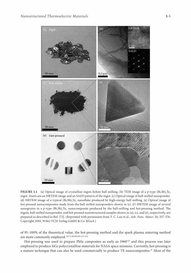
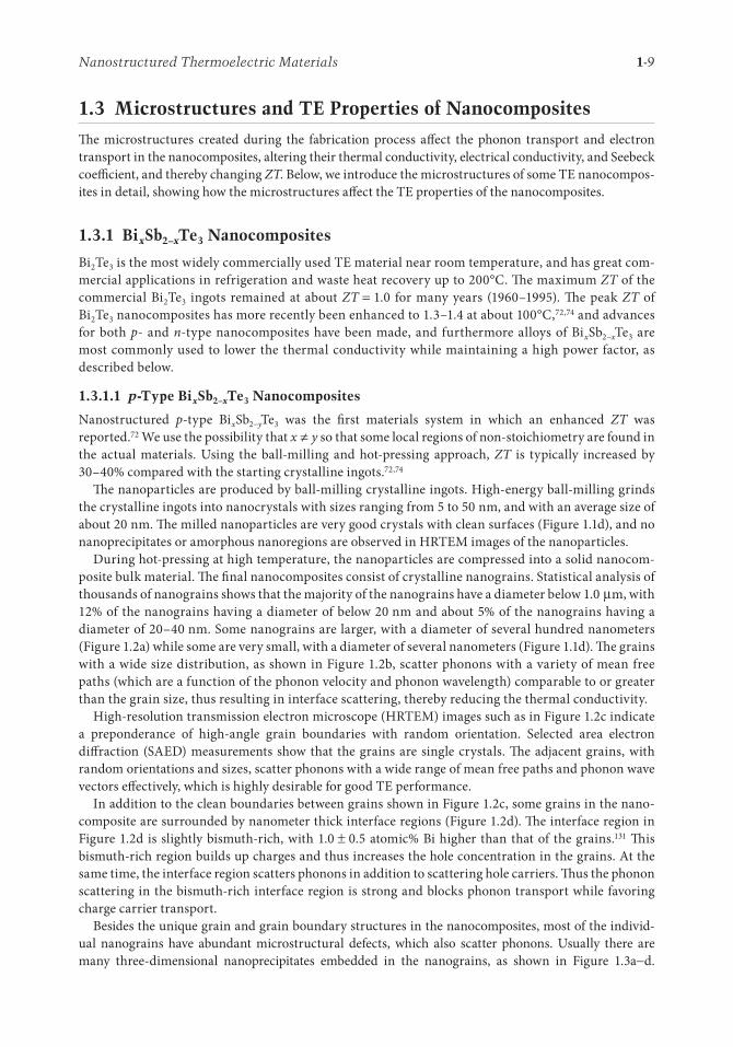
Among these methods, ball-milling is an e¤ective top-down industrial approach to obtain �ne par-ticles. Conventional ball-milling has been employed to produce large quantities of �ne particles with a size of one to several microns, and this process can be readily scaled up for commercial use at reason-able cost. High-energy ball-milling, developed in the 1970s as an industrial process, can create nanoparticles with a size as small as several nanometers.111 It has been proven that high-energy ball-milling is an e¤ective and powerful processing technique to produce large quantities of TE nanopar-ticles in a short time.77 Figure 1.1a,b shows crystalline ingots and the crystallinity of a p-type (Bi,Sb)2Te3 ingot before ball-milling. �e ingot is a bulk assembly of single crystal material. A¸er ball-milling, nanoparticles can be obtained (Figure 1.1c,d). Besides grinding down crystalline Bi2Te3 ingots, TE nanoparticles can also be prepared directly from the individual elements Bi and Te using a ball-milling method.73–77,102,112–114
1.2.2 Bottom-Up Methods to Produce Nanocomposites
In order to obtain TE nanocomposite materials, the TE nanoparticles are assembled into a dense solid using various bottom-up methods, such as spark plasma sintering,98,99,103,107–109,115 cold-pressing,100,101,104,116 sintering,37,101,117,118 hot-pressing,72,73,96,105,119–121 and extrusion methods.101,122
Among these methods, cold-pressing only mechanically compacts the nanoparticles and thus the density of cold-pressed composites tends to be low, resulting in a material with poor mechanical proper-ties. To improve the mechanical and electrical properties of the composites, the cold-pressing can be followed by sintering at appropriate temperatures. However, to reliably create composites with a density
1-5Nanostructured Thermoelectric Materials
of 95–100% of the theoretical value, the hot-pressing method and the spark plasma sintering method are more commonly employed.34,72,98,99,103,123,124
Hot-pressing was used to prepare PbSe composites as early as 1960125 and this process was later employed to produce SiGe polycrystalline materials for NASA space missions. Currently, hot-pressing is a mature technique that can also be used commercially to produce TE nanocomposites.47 Most of the
FIGURE 1.1 (a) Optical image of crystalline ingots before ball milling. (b) TEM image of a p-type (Bi,Sb)2Te3 ingot. Insets are an HRTEM image and an SAED pattern of the ingot. (c) Optical image of ball-milled nanopowder. (d) HRTEM image of a typical (Bi,Sb)2Te3 nano¡ake produced by high-energy ball milling. (e) Optical image of hot-pressed nanocomposites made from the ball-milled nanopowders shown in (c). (f) HRTEM image of several nanograins in a p-type (Bi,Sb)2Te3 nanocomposite produced by the ball-milling and hot-pressing method. �e ingots, ball-milled nanopowder, and hot-pressed nanostructured samples shown in (a), (c), and (e), respectively, are prepared as described in Ref. [72]. (Reprinted with permission from Y. C. Lan et al., Adv. Func. Mater. 20, 357–376. Copyright 2010, Wiley-VCH Verlag GmbH & Co. KGaA.)
1-6 Modules, Systems, and Applications in Thermoelectrics
recently reported nanocomposites with high ZT have been prepared using the hot-pressing technique described in Section 1.2.3.
�e technique used to produce nanocomposites can be any combination of a nanoparticle prepara-tion method and a bottom-up nanocomposite assembly method. Based on the various combinations, many nanocomposite preparation methods are possible. Table 1.1 lists some typical nanocomposite preparation techniques. Under appropriate processing conditions, the nanocomposite TE materials thus produced have a reduced thermal conductivity and a higher ZT. For example, a peak ZT of 1.4 has been achieved in p-type BixSb2−xTe3 nanocomposites produced by the ball-milling and hot-pressing method,72 compared to a peak ZT = 1.0 for the conventional bulk materials.
1.2.3 Ball-Milling and Hot-Pressing Method
�e ball-milling and hot-pressing method has been employed to produce TE composites since the 1960s.126 Interested readers are referred to earlier articles on ball-milling and hot-pressing methods in the literature.34,113,124,126 In earlier works, only micron-sized particles were obtained from ball-milling. �e grain size of these composites varies from several microns to 100 μm. As a result, the thermal con-ductivity of these hot-pressed composites was decreased compared with that of the single crystal,34,36 and the peak ZT of the resulting SiGe composites, consisting of micron-sized grains, was increased, but only by less than 20%.
Since the invention of high-energy ball-milling, large quantities of nanoparticles can be produced. A¸er hot-pressing, the grains in the nanocomposites still have a size in the nanometer range, although grain growth can take place during hot-pressing (Figure 1.1f).
�e combination of high-energy ball-milling and hot-pressing is very attractive from a commercial point of view because large quantities of nanopowders can be ball-milled and hot-pressed in a short time. From the research point of view, this method can prepare many TE materials with di¤erent chemical compositions and doping levels in a short time, allowing systematic studies to be carried out e´ciently.
Figure 1.1e shows several hot-pressed nanocomposite samples made from the ball-milled nanoparti-cles. Figure 1.1f shows the microstructure of a p-type (Bi,Sb)2Te3 nanocomposite made from ball-milling and hot-pressing. �e grain size is below 1 μm. Compared with other bottom-up methods, the ball-milling and hot-pressing method can produce dense bulk samples with a high density. For example, the density of the hot-pressed nanocomposites is higher than 98%,34 and even a density of 100%72 compared to that of single crystalline material has been achieved. �e hot-pressed nanocomposites are also ther-mally stable at high temperature and thermoelectrically isotropic.72–74
�e high-energy ball-milling and hot-pressing method has been employed to prepare many TE nano-composites, for example, Bi2Te3,39,72,74,105 SiGe alloys,73,75,76 and skutterudite CoSb3
127–129 nanocomposite materials. Table 1.1 summarizes some reported n- and p-type TE nanocomposites prepared by the ball-milling and hot-pressing method and some pertinent information about each is given in this table.
1.2.4 Chemical Synthesis and the Spark Plasma Sintering Method
Besides the ball-milling and hot-pressing method, some nanocomposites have been successfully produced by a chemical synthesis and spark plasma sintering method. In this method, the TE nanopar-ticles are �rstly synthesized by a chemical method. �e size distribution, nanoparticle shape, and quality of the nanoparticles can be �nely tuned by the parameters of the preparation process.130 A¸er spark plasma sintering, fully dense nanocomposites are produced.
Hot-pressing is a pressure-assisted sintering process, in which a direct-current or alternating current produces the required high temperature in the sample heating process. Spark plasma sintering is another kind of pressure-assisted sintering process, in which a pulsed direct-current source produces spark dis-charges to heat samples under high pressure. Both techniques have successfully produced �ne-grained nanostructured TE bulk materials with high density.
1-7Nanostructured Thermoelectric Materials
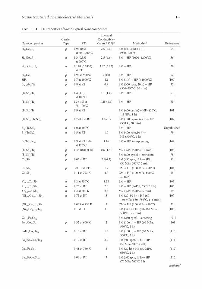
TABLE 1.1 TE Properties of Some Typical Nanocomposites
NanocompositesCarrier
Type ZT a
�ermal Conductivity (W m−1 K−1)a,b Methodsc,d References
Si80Ge20Bx p 0.95 (0.5) at 800–900°C
2.5 (5.0) BM (10–60 h) + HP (950–1200°C)
[54]
Si80Ge20P2 n 1.3 (0.93) at 900°C
2.5 (4.6) BM + HP (1000–1200°C) [56]
Si63.5Ge36.5Px n 0.128 (0.0937) at RT
3.82 (5.07) BM + HP [28]
Si95Ge5 p 0.95 at 900°C 5 (10) BM + HP [57]SiPx n 0.7 at 1000°C 12 BM (1 h) + HP (>1000°C) [100]Bi0.5Sb1.5Te3 p 0.8 at RT 0.9 BM (300 rpm, 20 h) + HP
(300–550°C, 30 min)[33]
(Bi,Sb)2Te3 p 1.4 (1.0) at 100°C
1.1 (1.4) BM + HP [53]
(Bi,Sb)2Te3 p 1.3 (1.0) at 75–100°C
1.25 (1.4) BM + HP [55]
(Bi,Sb)2Te3 p 0.9 at RT BM (400 cycles) + HP (420°C, 1.2 GPa, 1 h)
[101]
(Bi,Sb)2(Te,Se)3 p 0.7–0.9 at RT 1.0–1.5 BM (1200 rpm, 6.5 h) + HP (550°C, 30 min)
[102]
Bi2(Te,Se)3 n 1.0 at 100°C BM + HP UnpublishedBi2(Te,Se)3 n 0.5 at RT 1.0 BM (400 rpm,10 h) +
HP (500°C, 4 h)[79]
Bi2Te2.7Se0.3 n 0.9 at RT 1.04 at 125°C
1.16 BM + HP + re-pressing [147]
(Bi,Sb)2Te3 p 1.35 (0.8) at RT 0.6 (1.4) MS + SPS (510°C, 10 min) [103](Bi,Sb)2Te3 p BM (800 cycle) + extrusion [78]Co4Sb12 p 0.05 at RT 2.9(4.3) BM (450 rpm, 15 h) + SPS
(50 MPa, 300°C, 5 min)[82]
Co4Sb12 p <0.01 at RT 1.7 CM + HP (100 MPa, 450°C) [104]Co4Sb12 0.11 at 723 K 4.7 CM + HP (100 MPa, 600°C,
30 min)[95]
Yb0.35Co4Sb12 n 1.2 at 550°C 1.52 BM + HP [105]Yb0.19Co4Sb12 n 0.26 at RT 2.6 BM + HP (26PSI, 650°C, 2 h) [106]Yb0.29Co4Sb12 n 1.3 at 800 K 2.5 MS + SPS (550°C, 5 min) [89](Ni0.09Co0.91)4Sb12 n 0.75 at RT 3 BM (20–50 h) + HP (60–
160 MPa, 550–780°C, 1–6 min)[107]
(Ni0.08Co0.92)4Sb12 0.065 at 450 K 5 CM + HP (100 MPa, 450°C) [72](Ni0.8Co0.2)4Sb12 0.1 at RT 3.0 BM (39 h) + HP (80–160 MPa,
500°C, 1–5 min)[108]
Co4-xFexSb12 BM (230 rpm) + sintering [91]Fe1.5Co2.5Sb12 p 0.32 at 600 K 2 BM (100 h) + HP (60 MPa,
550°C, 2 h)[109]
SnFe3Co5Sb24 n 0.15 at RT 1.5 BM (100 h) + HP (60 MPa, 550°C, 2 h)
[110]
Lax(Ni,Co)3Sb12 0.12 at RT 3.2 BM (400 rpm, 10 h) + HP (50 MPa, 600°C, 2 h)
[111]
La1.5Fe4Sb12 0.41 at 750 K 2 BM (20 h) + HP (50 MPa, 650°C, 2 h)
[112]
La0.4FeCo3Sb12 0.04 at RT 3 BM (400 rpm, 14 h) + HP (70 MPa, 700°C, 3 h
[113]
continued
1-8 Modules, Systems, and Applications in Thermoelectrics
TABLE 1.1 (continued) TE Properties of Some Typical Nanocomposites
NanocompositesCarrier
Type ZT a
�ermal Conductivity (W m−1 K−1)a,b Methodsc,d References
β-FeSi2 0.018 at RT 4.5 BM (4 h) + HP (80–100 MPa, 950°C, 30 min)
[114]
Half-Heusler p 0.8 at 700°C 4.7 BM + HP [216]Fe0.95Co0.05Si2 n 0.18 at 923 K 4.5 BM (300 rpm,
30 min) + HP (50 MPa, 950°C, 30 min)
[115]
Mg2Si0.4Sn0.6 0.13 at 653 K 2.1 BM (600 cycle) + HP [116]Mg2Si0.6Ge0.4 p 0.21 at 610 K 4.3 BM (600 cycle) + HP (1 GPa,
500°C)[117]
TiNiSn0.95Sb0.05 4 (10) BM (18 h) + shock compaction (>5 GPa)
[118]
TiOx n <0.025 at RT 2.7–5.7 HP (114 MPa, 1200°C, 2 min) [119]Bi85Sb15 0.3 at 150 K 2.1 BM (236 rpm) + extrusion [75]PbTe n 0.07 at RT 4 BM + SPS (40 MPa, 310–510°C,
1–10 min)[77]
GaSb10Te16.5 p 0.6 at RT 1.2 BM (350 rpm, 5 h) + SPS (40 MPa)
[120]
Ag0.8Pb22SbTe20 1.37 at 673 K BM + SPS (50 MPa, 10 min) [81]2 wt%ZrO2 + β-FeSi2 0.14 (0.35)
at 700 K4.5 (5.0) BM (20 h) + HP (25 MPa,
900°C, 1 h)[121]
2 wt%Y2O3 + β-FeSi2 0.064 (0.035) at 700 K
4.5 (5.5) BM (20 h) + HP (25 MPa, 900°C, 1 h)
[122]
5 wt%TiB2 + β-FeSi2 0.015 (0.018) at RT
5.2 (4.5) BM (4 h) + HP (80–100 MPa, 950°C, 30 min)
[114]
50% Bi2Te3 + 50% Sb2Te3 1.47 at 450 K 1.1 HS + HP (75 MPa, 350°C, 15 min)
[71]
10 wt%Bi2Te3 nanoparticle + Bi0.5Sb1.5Te3 microparticle
0.65 at RT 0.55 BM + HP (50 MPa, 310°C, 30 min)
[123]
10 wt%Bi2Te3 nanoparticle + Bi2Te2.85Se0.15 microparticle
0.83 at 350 K 0.55 BM + HP (50 MPa, 310°C, 30 min)
[123]
7 wt%BN + (Bi0.2Sb0.8)2Te3 0.54 (1.0) at RT 1.2 (1.5) BM (1200 rpm, 5 h) + HP (425 MPa, 550°C, 30 min)
[124]
7 wt%WO3 + (Bi0.2Sb0.8)2Te3 0.75 (1.0) at RT 1.3 (1.5) BM (1200 rpm, 5 h) + HP (425 MPa, 550°C, 30 min)
[124]
15 wt% nanoplate Bi2Te3 + Bi2Te3
0.39 at RT 1.1 Plasma sintering [125]
25.4 vol%TiB2 + B4C 0.002 (0.01) at 1050 K
16 (9) BM (10 h) + HP (35 MPa, 1900°C, 30 min)
[165]
a Data within parentheses are the values of single crystals or of nanocomposites without addition of second phase material.b At room temperature (RT).c BM, ball-milling; HS, hydrothermal synthesis; CM, chemical method; MS, melt spinning; HP, hot-pressing; CP, cold-
pressing; SPS, spark plasma sintering.d Experimental details are listed within parentheses.
1-9Nanostructured Thermoelectric Materials
1.3 Microstructures and TE Properties of Nanocomposites
�e microstructures created during the fabrication process a¤ect the phonon transport and electron transport in the nanocomposites, altering their thermal conductivity, electrical conductivity, and Seebeck coe´cient, and thereby changing ZT. Below, we introduce the microstructures of some TE nanocompos-ites in detail, showing how the microstructures a¤ect the TE properties of the nanocomposites.
1.3.1 BixSb2–xTe3 Nanocomposites
Bi2Te3 is the most widely commercially used TE material near room temperature, and has great com-mercial applications in refrigeration and waste heat recovery up to 200°C. �e maximum ZT of the commercial Bi2Te3 ingots remained at about ZT = 1.0 for many years (1960–1995). �e peak ZT of Bi2Te3 nanocomposites has more recently been enhanced to 1.3–1.4 at about 100°C,72,74 and advances for both p- and n-type nanocomposites have been made, and furthermore alloys of BixSb2−xTe3 are most commonly used to lower the thermal conductivity while maintaining a high power factor, as described below.
1.3.1.1 p-Type BixSb2–xTe3 Nanocomposites
Nanostructured p-type BixSb2−yTe3 was the �rst materials system in which an enhanced ZT was reported.72 We use the possibility that x ≠ y so that some local regions of non-stoichiometry are found in the actual materials. Using the ball-milling and hot-pressing approach, ZT is typically increased by 30–40% compared with the starting crystalline ingots.72,74
�e nanoparticles are produced by ball-milling crystalline ingots. High-energy ball-milling grinds the crystalline ingots into nanocrystals with sizes ranging from 5 to 50 nm, and with an average size of about 20 nm. �e milled nanoparticles are very good crystals with clean surfaces (Figure 1.1d), and no nanoprecipitates or amorphous nanoregions are observed in HRTEM images of the nanoparticles.
During hot-pressing at high temperature, the nanoparticles are compressed into a solid nanocom-posite bulk material. �e �nal nanocomposites consist of crystalline nanograins. Statistical analysis of thousands of nanograins shows that the majority of the nanograins have a diameter below 1.0 μm, with 12% of the nanograins having a diameter of below 20 nm and about 5% of the nanograins having a diameter of 20–40 nm. Some nanograins are larger, with a diameter of several hundred nanometers (Figure 1.2a) while some are very small, with a diameter of several nanometers (Figure 1.1d). �e grains with a wide size distribution, as shown in Figure 1.2b, scatter phonons with a variety of mean free paths (which are a function of the phonon velocity and phonon wavelength) comparable to or greater than the grain size, thus resulting in interface scattering, thereby reducing the thermal conductivity.
High-resolution transmission electron microscope (HRTEM) images such as in Figure 1.2c indicate a preponderance of high-angle grain boundaries with random orientation. Selected area electron di¤raction (SAED) measurements show that the grains are single crystals. �e adjacent grains, with random orientations and sizes, scatter phonons with a wide range of mean free paths and phonon wave vectors e¤ectively, which is highly desirable for good TE performance.
In addition to the clean boundaries between grains shown in Figure 1.2c, some grains in the nano-composite are surrounded by nanometer thick interface regions (Figure 1.2d). �e interface region in Figure 1.2d is slightly bismuth-rich, with 1.0 ± 0.5 atomic% Bi higher than that of the grains.131 �is bismuth-rich region builds up charges and thus increases the hole concentration in the grains. At the same time, the interface region scatters phonons in addition to scattering hole carriers. �us the phonon scattering in the bismuth-rich interface region is strong and blocks phonon transport while favoring charge carrier transport.
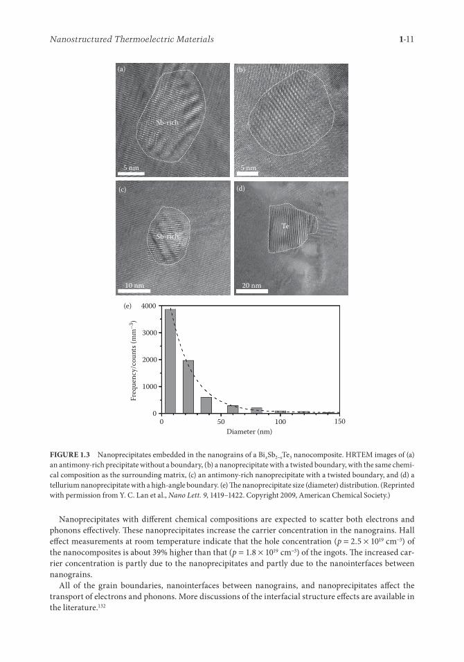
Besides the unique grain and grain boundary structures in the nanocomposites, most of the individ-ual nanograins have abundant microstructural defects, which also scatter phonons. Usually there are many three-dimensional nanoprecipitates embedded in the nanograins, as shown in Figure 1.3a−d.
1-10 Modules, Systems, and Applications in Thermoelectrics
In BixSb2−xTe3 nanocomposites, at least four kinds of nanoprecipitates, as enumerated below, are observed in the crystalline nanograins. A common type of nanoprecipitates is an antimony-rich nanoprecipitate (Figure 1.3a). �ere are no obvious boundaries between the nanoprecipitates and nanograin matrix, with even no obvious lattice distortion between them. �e lattice is continuous and the fringe spacing is almost the same. In the HRTEM images in Figure 1.3, the nanoprecipitates are brighter than the surrounding crystalline matrix. Another type of nanoprecipitate is a nanodot with an orientation that is twisted with respect to that of the matrix. �e chemical composition of the nanodot is the same as that of the surround-ing matrix. �e third type of nanoprecipitate (Figure 1.3c) is also twisted from the surrounding matrix and is also antimony rich. �is type of nanoprecipitate is the combination of type one and type two nanopre-cipitates. �e fourth type is a pure tellurium nanodot (Figure 1.3d). �ese polygonal tellurium precipitates are easily identi�ed structurally from the other three types of irregular nanoprecipitates.
�e types of nanoprecipitates described above are very similar to those observed in Ag1−xPbmSbTem+2 alloys.23–26 It is believed that the presence of these nanoprecipitates as scattering centers are responsible for the ZT enhancement in these alloys. Experiments have shown that the nanometer-sized precipitates embedded in a crystalline host, like 30–40 nm Pb or Au metal particles in crystalline PbTe samples, can at the same time increase the TE power factor and reduce the thermal conductivity.57,79 In the BixSb2−xTe3 nanocomposites, it is expected that these nanoprecipitates predominately scatter phonons and reduce the thermal conductivity. We therefore need to look for more opportunities to further increase the power factor and thereby increase ZT.
0.0 1.0 2.0 3.0Diameter (μm)
30(b)
(d)(c)
(a)Grain 2
Grain 1Grain 3
Grain 4
Grain 2
Grain 2
Bi-r
ich in
terfa
ce
Grain 3
Grain 1
Grain 1
0.5 μm
10 nm 5 nm
10
5
00.0 0.1 0.2
20
10Coun
ts (%
)
0
FIGURE 1.2 (a) Bright-�eld TEM image of multigrains and (b) grains size distribution. HRTEM images of (c) clean grain boundaries and (d) an interface region between two grains in a p-type BixSb2−xTe3 nanocomposite. �e inset in (b) is a zoom of the small diameter region of the larger �gure. (Reprinted with permission from Y. C. Lan et al., Nano Lett. 9, 1419–1422. Copyright 2009, American Chemical Society.)
1-11Nanostructured Thermoelectric Materials
Nanoprecipitates with di¤erent chemical compositions are expected to scatter both electrons and phonons e¤ectively. �ese nanoprecipitates increase the carrier concentration in the nanograins. Hall e¤ect measurements at room temperature indicate that the hole concentration (p = 2.5 × 1019 cm−3) of the nanocomposites is about 39% higher than that (p = 1.8 × 1019 cm−3) of the ingots. �e increased car-rier concentration is partly due to the nanoprecipitates and partly due to the nanointerfaces between nanograins.
All of the grain boundaries, nanointerfaces between nanograins, and nanoprecipitates a¤ect the transport of electrons and phonons. More discussions of the interfacial structure e¤ects are available in the literature.132
4000
3000
2000
1000
00 50
(c)
Sb-rich
10 nm
(d)
20 nm
Te
Sb-rich
5 nm
(a)
5 nm
(b)
(e)
100Diameter (nm)
Freq
uenc
y/co
unts
(mm
–3)
150
FIGURE 1.3 Nanoprecipitates embedded in the nanograins of a BixSb2−xTe3 nanocomposite. HRTEM images of (a) an antimony-rich precipitate without a boundary, (b) a nanoprecipitate with a twisted boundary, with the same chemi-cal composition as the surrounding matrix, (c) an antimony-rich nanoprecipitate with a twisted boundary, and (d) a tellurium nanoprecipitate with a high-angle boundary. (e) �e nanoprecipitate size (diameter) distribution. (Reprinted with permission from Y. C. Lan et al., Nano Lett. 9, 1419–1422. Copyright 2009, American Chemical Society.)
1-12 Modules, Systems, and Applications in Thermoelectrics
Besides the nanoprecipitates, there are two-, one-, and zero-dimensional defects in the nanograins of the nanocomposites.131 TEM investigation indicates that stacking faults exist in the nanograins. �e threading dislocation concentration is ~1011 cm−2 in nanograins, at least 10 times higher than that in the crystalline ingots (~5 × 109 cm−2). �e point defect concentration in nanograins is 2–3 orders of magni-tude higher than that in the ingot. Structural modulations are also observed in the nanograins even though the concentration of structural defects is almost the same as that in the ingots. All these defects would scatter phonons more e¤ectively and decrease the thermal conductivity of the nanocomposites.
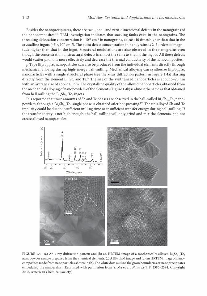
p-Type BixSb2−xTe3 nanoparticles can also be produced from the individual elements directly through mechanical alloying during high-energy ball-milling. Mechanical alloying can synthesize BixSb2−xTe3 nanoparticles with a single structural phase (see the x-ray di¤raction pattern in Figure 1.4a) starting directly from the element Bi, Sb, and Te.74 �e size of the synthesized nanoparticles is about 5–20 nm with an average size of about 10 nm. �e crystalline quality of the alloyed nanoparticles obtained from the mechanical alloying of nanopowders of the elements (Figure 1.4b) is almost the same as that obtained from ball milling the BixSb2−xTe3 ingots.
It is reported that trace amounts of Sb and Te phases are observed in the ball-milled BixSb2−xTe3 nano-powders although a BixSb2−xTe3 single phase is obtained a¸er hot-pressing.133 �e un-alloyed Sb and Te impurity could be due to insu´cient milling time or insu´cient transfer energy during ball-milling. If the transfer energy is not high enough, the ball-milling will only grind and mix the elements, and not create alloyed nanoparticles.
(c) HRTEM
5 nm
200 nm 5 nm
(d)
5 nm
(b)
15 20
(a)
30 402θ (degree)
Inte
nsity
(a.u
.) (0 1
5)
(0 0
6)
(0 1
8) (10
10)
(1 1
0)(0
0 1
5)(1
0 1
3)
(205
)
(02
10)
50
FIGURE 1.4 (a) An x-ray di¤raction pattern and (b) an HRTEM image of a mechanically alloyed BixSb2−xTe3 nanopowder sample prepared from the chemical elements. (c) A BF-TEM image and (d) an HRTEM image of nano-composites made from nanoparticles shown in (b). �e white dots outline the grain boundaries or nanoprecipitates embedding the nanograins. (Reprinted with permission from Y. Ma et al., Nano Lett. 8, 2580–2584. Copyright 2008, American Chemical Society.)
1-13Nanostructured Thermoelectric Materials
�e microstructure of the nanocomposite made from the elements is very similar to that of the nanocomposite made from ingots of the same elemental composition for the starting materials. �e nanograin size is in the sub-micrometer range and the nanocomposites are densely packed (Figure 1.4c). Compared with the starting mechanically alloyed nanopowders (Figure 1.4b), the nanograins in nano-composites grow to larger sizes a¸er hot-pressing (Figure 1.4c). Detailed TEM studies indicate that nanoprecipitates are also formed and embedded inside the BixSb2−xTe3 nanograins (Figure 1.4d), very similar to the nanoscale morphology of the hot-pressed nanocomposites made from the ingots (Figure 1.3a−d).
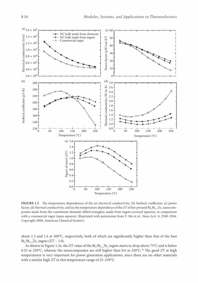
�ese unique microstructures (shown in Figures 1.2 through 1.4) are important for obtaining superior TE properties of the nanocomposites. In Figure 1.5, we compare the transport properties of three samples: the hot-pressed nanocomposite made from the Bi, Sb, and Te elements, the hot-pressed nanocomposite made from the crystalline BixSb2−xTe3 ingots, and the crystalline ingot itself.74
�e electrical conductivity of the BixSb2−xTe3 nanocomposites is always higher than that of the crystalline ingots (Figure 1.5a) because of the higher carrier concentration (2.9 × 1019 cm−3 for the nanocomposites and 1.8 × 1019 cm−3 for the ingots at room temperature).74 Here the nanoprecipitates embedded in the nanograins and nanointerfaces should contribute to the increase of the electrical conductivity. �e enhancement of electrical conductivity is very important to improve the ZT of nanocomposites. Since the 1960s, much work has been carried out in low-dimensional composites, and ZT could not be increased because of the decrease of the electrical conductivity. Although pho-nons are scattered greatly by the grain boundaries, resulting in a decrease in the thermal conductiv-ity, electrons are also scattered by the grain boundaries, resulting in a decrease in the electrical conductivity. According to Equation 1.1, ZT increases or decreases depending on the relative values of the thermal conductivity and the electrical conductivity when the Seebeck coe´cient remains constant.
�e Seebeck coe´cient (Figure 1.5b) of both BixSb2−xTe3 nanocomposites is lower than that of the crystalline ingot sample below 150°C but is higher above 150°C.74 �e smaller magnitude of the Seebeck coe´cient near room temperature is due to a higher carrier concentration, while the larger Seebeck coe´cient at higher temperatures is due to the suppression of minority carrier (electron) excitation in heavily doped samples.
�e thermal conductivities of both types of nanocomposites in Figure 1.5 are signi�cantly lower than that of the ingot because of the presence of abundant grain boundaries in the nanocomposites, and the thermal conductivities of both types of nanocomposites increase more slowly with increasing temperature than does the thermal conductivity of the ingot (Figure 1.5d).74 Comparing the properties of the nanocomposite made from the elements with that made from the ingot, the thermal conductivity of the nanocomposite made from the elements is systematically higher than that of the nanocomposite made from ingot. �e di¤erence is probably due to compositional di¤erences arising from the lack of some trace amount of elements that were used in the process of making the ingot and to some structural di¤erences in the two types of samples.
�e nanocomposite made from BixSb2−xTe3 ingots has a power factor comparable to that of the crystal-line ingot below 100°C but is higher above 100°C. �e nanocomposites made from the Bi, Sb, and Te elements in Figure 1.5 have a slightly lower power factor than those made from the ingots. �e power factor increase is likely due to some energy �ltering e¤ect at grain boundaries.
According to Equation 1.1, ZT for the nanocomposite BixSb2−xTe3 should be enhanced because the thermal conductivity decreases signi�cantly while the electrical conductivity increases and the Seebeck coe´cient changes only slightly. Figure 1.5e shows the resulting temperature dependence of ZT for the hot-pressed nanocomposites made from the Bi, Sb, and Te elements and from the ingots, in comparison with that of the commercial BixSb2−xTe3 ingots. �e peak ZT values for both types of nanocomposites shi¸ to a higher temperature and remain signi�cantly higher than that of the ingots at all tempera-tures.74 �e peak ZT values of the hot-pressed nanocomposites made from the elements and ingots are
1-14 Modules, Systems, and Applications in Thermoelectrics
about 1.3 and 1.4 at 100°C, respectively, both of which are signi�cantly higher than that of the best BixSb2−xTe3 ingots (ZT ~ 1.0).
As shown in Figure 1.5e, the ZT value of the BixSb2−xTe3 ingots starts to drop above 75°C and is below 0.25 at 250°C, whereas the nanocomposites are still higher than 0.6 at 250°C.74 �e good ZT at high temperatures is very important for power generation applications, since there are no other materials with a similar high ZT in this temperature range of 25–250°C.
Temperature (°C)
120
Seeb
eck
coeffi
cien
t (μV
/K)
0 50 100 150Temperature (°C)
200 250
140
160
180
200
220
240
260(b)
60
50
40
30
20
10
0
Pow
er fa
ctor
(μW
/cm
-K2 )
(c)
2.82.62.42.22.01.81.61.41.21.00.8
er
mal
cond
uctiv
ity (W
/m-K
)
0 50 100 150 200 250
(d)
1.6
1.4
1.2
1.0
0.8
0.6
0.4
0.2
0.00 50 100 150
Temperature (°C)
Figu
re o
f mer
it (Z
T )
200 250
(e)
Elec
tric
al co
nduc
tivity
(S/m
)(a)
NC bulk made from elementsNC bulk made from ingotsCommercial ingot
1.6 × 10⁵
1.4 × 10⁵
1.2 × 10⁵
1.0 × 10⁵
8.0 × 10⁴
6.0 × 10⁴
4.0 × 10⁴
2.0 × 10⁴
FIGURE 1.5 �e temperature dependences of the (a) electrical conductivity, (b) Seebeck coe´cient, (c) power factor, (d) thermal conductivity, and (e) the temperature dependence of the ZT of hot-pressed BixSb2–xTe3 nanocom-posites made from the constituent elements (�lled triangles), made from ingots (crossed squares), in comparison with a commercial ingot (open squares). (Reprinted with permission from Y. Ma et al., Nano Lett. 8, 2580–2584. Copyright 2008, American Chemical Society.)
1-15Nanostructured Thermoelectric Materials
Using the ball-milling and hot-pressing method, other groups have also prepared p-type BixSb2−xTe3 nanocomposites34,39,133–138 and p-type (Bi,Sb)2(Te,Se)3 nanocomposites.139 In these works, ZT is less than 1.0 and lower than that of the crystalline ingots. �ere are many reasons why ZT could decrease, with the most likely cause being a decrease in the electrical conductivity. �e electrical conductivity of the nanocomposites is very sensitive to oxygen, moisture, and other environmental factors. A decrease in the electrical conductivity results in a cancellation of the bene�ts derived from the decreased thermal conductivity of these nanostructures to ZT. In order to achieve good electrical conductivity, the TE materials should be kept away from oxygen and moisture.
Using a ball-milling and hot-pressing method, p-type (Bi,Sb)2Te3 composites composed of 100 μm particles and 15–30 nm Bi2Te3 nanoparticles were also obtained.140 For each samples, a peak ZT of 0.83 was achieved. �is result shows the importance of reducing the amount of large size particles in the composite.
p-Type (Bi,Sb)2Te3 nanocomposites have also been prepared by other methods, such as by a shear extrusion method at high temperatures from ball-milled powder,104 by a hot-pressing method from hydrothermally synthesized nanoparticles,95 and by melting spinning and spark plasma sintering.141 Results obtained with other nanocomposites and detailed information about the results are listed in Table 1.1. Among them, one interesting nanocomposite is a p-type Bi2Te3 nanocomposite with a layered nanostructure.141 �e nanocomposite bulk material that is obtained in this case consists of Bi2Te3 nano-layers with a thickness of 10–40 nm, similar to the structure of the Bi2Te3/Sb2Te3 superlattices prepared by molecular-beam epitaxy.51–54 �e large number of interfaces in the superlattice samples reduce the lattice thermal conductivity extraordinarily to the low value of 0.58 W m−1 K−1. A peak ZT of 1.35 is obtained at 300 K when using this nanocomposite, and an increase of 73% is obtained over that for the ZT of the ingot, showing the e¤ectiveness of this method of sample preparation. However, the scale-up of this method for commercial scale production would be challenging.
1.3.1.2 n-Type Bi2Te3–ySey Nanocomposites
n-Type Bi2Te3−ySey nanocomposites can also be prepared using the various methods, as mentioned below. One notable attribute about the Bi2Te3-based single-crystal nanostructural bulk samples is the lamellar structure and the weak van der Waals bonding between Te(1) atoms [locate at (1/3, 2/3, 0.457) atomic position in the unit cell] and Te(1) atoms [locate at (2/3,1/3,0.523) atomic position in the unit cell], which is responsible for the easy cleavage along the planes perpendicular to the c-axis.3,142 Originating from this unique structural anisotropy of Bi2Te3, the TE properties of n-type Bi2Te3−ySey single-crystal solid solutions prepared by the traveling heater method shows a strong anisotropy.143 �e electrical and thermal conductivities along the cleavage planes (perpendicular to the c-axis) are, respectively, about four and two times larger than those along the c-axis. Even though the Seebeck coe´cient in Bi2Te3 is nearly isotropic, the TE �gure-of-merit Z along the cleavage planes is approximately two times as large as that along the c-axis. At room temperature a maximum dimensionless TE �gure-of-merit was achieved at ZT = 0.85 (Z = 2.9 × 10⁻³ K−1) for solid solutions with a 2.5 at% Se replacing Te in the Bi2Te2.925Se0.075 alloy that has a power factor S2σ of 47 × 10−4 W m−1 K−2 and a thermal conductivity of 1.65 W m−1 K−1 in which the lattice contribution is 1.27 W m−1 K−1 (see Ref. 142).
In principle, ZT could be greatly improved if we can decrease the thermal conductivity by breaking a single crystal into individual nano size grains to thus greatly increase its phonon scattering due to the signi�cantly increased density of grain boundaries of the resulting nano grains34,144 while at the same time maintaining the high power factor by retaining the preferential orientation of the grains.145,146 We have successfully synthesized n-type Bi2Te2.7Se0.3 bulk samples by ball milling and dc hot pressing, and we have achieved a signi�cantly lower thermal conductivity of 1.06 W m−1 K−1 (with a lattice contribution of 0.7 W m−1 K−1, much lower than the 1.27 W m−1 K−1 in single crystals) due to the increased phonon scatter-ing by grain boundaries, in comparison to the 1.65 W m−1 K−1 value in the case of single-crystal bulk sam-ples.147 However, ZT was not enhanced at all because of a much lower power factor of 25 × 10−4 W m−1 K−2,147 in comparison to the 47 × 10−4 W m−1 K−2 in single-crystal bulk samples. We suspect that the reason for the
1-16 Modules, Systems, and Applications in Thermoelectrics
lower power factor is due to increased carrier scattering arising from the randomness of the small grains. �erefore, the challenge is to improve the power factor to a level close to that of the single-crystal-like nanostructural nanocomposite bulk samples while retaining the low thermal conductivity due to the �ne grains which scatter both phonons and electrons strongly. In the literature, there have been a few methods reported on how to prepare polycrystalline Bi2Te3-based bulk alloys with preferred grain orientations, such as by hot pressing148,149 and by hot extrusion.104,105,150 However, those reports were not about preparing samples with small grains of less than a couple of micrometers, but rather with large grains of many micrometers. �ere were also reports about melt spinning to improve the ZT.151,152 However, the important detailed aspects of their structural and property anisotropies were not discussed.
1.3.1.3 Partially Aligned
In this section we describe the experimental studies on the physical properties of samples with partial alignment of the small grains.147 To achieve grain alignment, we re-pressed the as-pressed n-type Bi2Te2.7Se0.3 bulk nanocomposite sample in a bigger diameter die at a higher temperature so that lateral ¡ow of the small grains takes place in the disk plane to achieve a certain orientation of the ab plane of the sample in the disk plane of the die. As a result, we increased the power factor by 40% in the disk plane direction from 25 × 10−4 to 35 × 10−4 W m−1 K−2 without too much penalty on the thermal conduc-tivity, leading to a peak ZT enhancement of 22% from 0.85 to 1.04.147 In contrast, the ZT along the press direction is decreased, which does not a¤ect the application of TE materials since only the direction with the highest ZT is used in devices.
Figure 1.6a,b shows the XRD patterns of both the planes perpendicular (⊥) and parallel (//) to the press direction, respectively, and Figure 1.6c,d shows the SEM images of the freshly fractured surfaces in the ⊥ and // directions, respectively. �ese two XRD spectra look the same for both the 2θ position and the intensity of each peak, indicating that there is no signi�cant grain orientation anisotropy. �e ratios of the integrated intensities of planes (006) and ( )0015 to that of the strongest peak (015) are shown in the insets. �e minor larger ratios of I(006)/I(015) (15% vs. 12%) and I I( ) ( )0015 015/ (12% vs. 8%) for the plane that is ⊥ to the
15
Inte
nsity
(a.u
.)
(006
)
(101
)
(018
)
(015
)
(101
0)
(011
1)(1
10)
(001
5)
20 25 302θ (degree)
Pressdirection
Pressdirection
As-pressed
2 μm
(c)
(d)
(a)
(b)
2 μm
I006/I015 = 12%I0015/I015 = 8%
As-pressedI006/I015 = 15%
I0015/I015 = 12%
35 40 45
FIGURE 1.6 XRD patterns of the as-pressed Bi2Te2.7Se0.3 bulk nanocomposite samples for the planes (a) perpen-dicular (⊥) and (b) parallel (//) to the press direction, and SEM images of the freshly fractured surfaces of as-pressed samples in the direction (c) perpendicular (⊥) and (d) parallel (//) to the press direction. (Reprinted with permission from X. Yan et al., Nano Lett. 10, 3373–3378. Copyright 2010, American Chemical Society.)
1-17Nanostructured Thermoelectric Materials
press direction (Figure 1.6a) mean that there is a little bit more ab orientation in the ⊥ direction, which is re¡ected by the physical properties (discussed below). From the SEM images (Figure 1.6c,d), we can see that the physical properties of these samples are consistent with the XRD result (Figure 1.6a,b): the grains are random without a signi�cant preferred crystal orientation. �e average grain size is about 1–2 μm even though there are many grains smaller than 1 μm.
In Figure 1.7, we show the transport properties of the as-pressed samples in both the directions perpendicu-lar (⊥) and parallel (//) to the press direction. �e electrical conductivity σ⊥ is about 12–15% higher than σ// for
0.5
ZT
1.4
1.2
(b) (d)
(c)(a)
(e)
1.0
0.8
0.6
0.4
0.2
0.00 50 100
Temperature (°C)150 200 250
0 50 100Temperature (°C)
150 200 250 0 50 100Temperature (°C)
150 200 250
0.7
0.9
1.1
1.3
1.5
5
10
15
20
25
30
359
8
7
6
5
4
3
2
// Press direction
Elec
tric
al co
nduc
tivity
(104 S
m–1
)
Ther
mal
cond
uctiv
ity (W
m–1
K–2
)Po
wer
fact
or (1
0–4 W
m–1
K–2)
Seeb
eck
coef
ficie
nt (μ
VK–1
)
// Press direction
// Press direction
// Press direction
// Press direction
⊥ Press direction ⊥ Press direction
⊥ Press direction
⊥ Press direction
⊥ Press direction
–100
–150
–200
–250
–300
FIGURE 1.7 �e temperature dependence from 50 < T < 250°C of the (a) electrical conductivity, (b) Seebeck coe´cient, (c) power factor, (d) thermal conductivity, and (e) ZT of the as-pressed samples in both the directions perpendicular (⊥) and parallel (//) to the press direction. (Reprinted with permission from X. Yan et al., Nano Lett. 10, 3373–3378. Copyright 2010, American Chemical Society.)
1-18 Modules, Systems, and Applications in Thermoelectrics
the whole temperature range (Figure 1.7a), which clearly shows that there is a little bit more ab plane orientation in the ⊥ direction, consistent with the results shown by the XRD (Figure 1.6a). �e Seebeck coe´cients of the as-pressed sample are very similar to each other in both directions (Figure 1.7b), consistent with the fact that the Seebeck coe´cient of single crystals is nearly isotropic in di¤erent crystal orientations.143 �e correspond-ing power factors of the as-pressed sample in both directions are shown in Figure 1.7c. A power factor (S2σ) of 25 × 10−4 W m−1 K−2 at room temperature was obtained for the ⊥ direction and the power factor drops down to 13 × 10−4 W m−1 K−2 at 250°C, while that in the // direction is about 15–19% lower in the temperature range. It is very important to note that the power factor of the as-pressed sample in either direction is much lower than the 47 × 10−4 W m−1 K−2 in the ab plane of the single crystals,143 which led us to think of a possibility for further improving ZT by enhancing the power factor through aligning the ab planes into the disk plane while keeping the thermal conductivity at the same low value. �e thermal conductivity dependences on temperature of the as-pressed samples in both directions are shown in Figure 1.7d. Over the whole temperature range, the thermal conductivity is much lower (1.06 W m−1 K−1 in the ⊥ direction and 0.92 W m−1 K−1 in the // direction with a lattice contribution of 0.7 and 0.6 W m−1 K−1, respectively) (a Lorenz number of about 1.6 × 10⁻⁸ J2 K−2 C−2 is used for the nano samples) than 1.65 W m−1 K−1 [with a lattice contribution of 1.27 W m−1 K−1 (see Ref. 142)] in the ab plane of the single crystals, a clear indication of the bene�ts of the stronger phonon scattering resulting from the smaller grains in the samples with partially aligned grains. Below 150°C, the thermal conductivity does not increase too much, but κ increases above 150°C due to the bipolar e¤ect, and the di¤erences in the thermal conductivity between the samples in the two directions become smaller and smaller with increasing temperature. Similar to the electrical conductivity, the thermal conductivity is also higher in the direction perpendicular to the press direction, which resulted in almost the same ZT dependence on temperature all the way up to 250°C in both directions, indicating an isotropic ZT (Figure 1.7e). �e peak ZT is about 0.85 and is about the same as that of the single crystals at room temperature.
Considering the potentially high power factor of 47 × 10−4 W m−1 K−2 in the ab plane of the single crystals, it is possible to enhance ZT by orienting the ab planes of the small grains into the disk plane. One way to orient the grains is to press the as-pressed samples in a bigger diameter die so that lateral ¡ow takes place.153
Figure 1.8 shows the XRD patterns of the re-pressed samples in the planes perpendicular (⊥) (Figure 1.8a) and parallel (//) (Figure 1.8b) to the press direction and the SEM images of the freshly fractured surfaces of the re-pressed samples in the plane perpendicular (⊥) (Figure 1.8c) and parallel (//) (Figure 1.8d) to the press direction. From the much stronger di¤raction intensities of the (006) and ( )0015 peaks (Figure 1.8a) and the much weaker intensities of the same peaks in Figure 1.8b, it is very clear that reorientation of the ab planes of the grains into the disk plane took place during the re-pressing process. �e ratios of the integrated intensities of the (006) and ( )0015 peaks to that of the strongest peak (015) in the ⊥ direction are 55% (I(006)/I(015)) and 44% ( )( ) ( )I I0015 015/ (inset in Figure 1.8a), which are much higher than those from the as-pressed samples (inset in Figure 1.6a), and much stron-ger than the 6% (I(006)/I(015)) and 3% ( )( ) ( )I I0015 015/ for the plane parallel to the press direction (inset in Figure 1.8b), respectively. On the one hand, the (006) and ( )0015 peak intensities increased a lot in the disk plane a¸er re-pressing (Figure 1.8a vs. 1.6a), and on the other hand, the intensity of the same peaks decreased a lot in the plane parallel to the press direction (Figure 1.8b vs. 1.6b). �e signi�cant di¤rac-tion peak intensity di¤erence shows that we have successfully developed a signi�cant anisotropy in the re-pressed samples, which should clearly show up in the microstructures and physical properties (dis-cussed below). From the SEM images (Figure 1.8c,d), we can clearly see that the grains are plate-like and with the ab plane preferentially oriented in the disk plane, which con�rms the much increased (00l) peak XRD intensities in the disk plane and the decreased (00l) peak intensities in the plane paral-lel to the press direction. Such a re-orientation of the ab planes is clearly the result of the lateral ¡ow during the re-pressing process.153 �e lateral ¡ow also makes the plates thinner due to the shear force. However, these plates are still quite large (up to 5 μm) and thick (up to 0.5 μm). Compared to the size before re-pressing, we can also see that a signi�cant grain growth had occurred (in plane). �e detailed
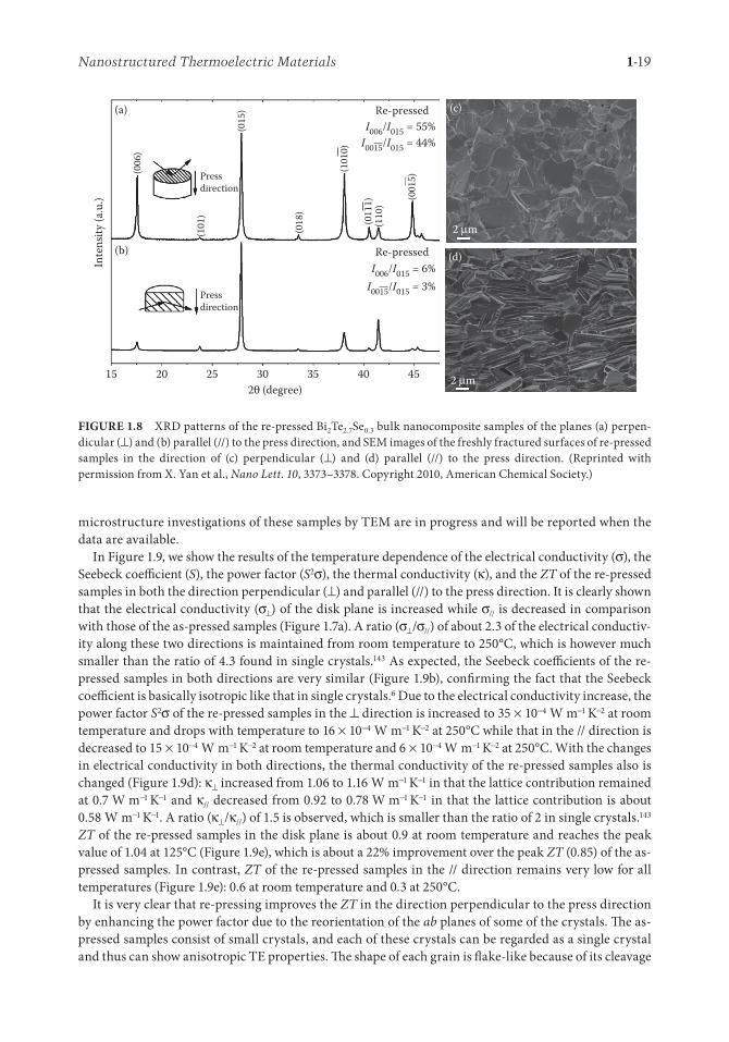
1-19Nanostructured Thermoelectric Materials
microstructure investigations of these samples by TEM are in progress and will be reported when the data are available.
In Figure 1.9, we show the results of the temperature dependence of the electrical conductivity (σ), the Seebeck coe´cient (S), the power factor (S2σ), the thermal conductivity (κ), and the ZT of the re-pressed samples in both the direction perpendicular (⊥) and parallel (//) to the press direction. It is clearly shown that the electrical conductivity (σ⊥) of the disk plane is increased while σ// is decreased in comparison with those of the as-pressed samples (Figure 1.7a). A ratio (σ⊥/σ//) of about 2.3 of the electrical conductiv-ity along these two directions is maintained from room temperature to 250°C, which is however much smaller than the ratio of 4.3 found in single crystals.143 As expected, the Seebeck coe´cients of the re-pressed samples in both directions are very similar (Figure 1.9b), con�rming the fact that the Seebeck coe´cient is basically isotropic like that in single crystals.6 Due to the electrical conductivity increase, the power factor S2σ of the re-pressed samples in the ⊥ direction is increased to 35 × 10−4 W m−1 K−2 at room temperature and drops with temperature to 16 × 10−4 W m−1 K−2 at 250°C while that in the // direction is decreased to 15 × 10−4 W m−1 K−2 at room temperature and 6 × 10⁻⁴ W m−1 K−2 at 250°C. With the changes in electrical conductivity in both directions, the thermal conductivity of the re-pressed samples also is changed (Figure 1.9d): κ⊥ increased from 1.06 to 1.16 W m−1 K−1 in that the lattice contribution remained at 0.7 W m−1 K−1 and κ// decreased from 0.92 to 0.78 W m−1 K−1 in that the lattice contribution is about 0.58 W m−1 K−1. A ratio (κ⊥/κ//) of 1.5 is observed, which is smaller than the ratio of 2 in single crystals.143 ZT of the re-pressed samples in the disk plane is about 0.9 at room temperature and reaches the peak value of 1.04 at 125°C (Figure 1.9e), which is about a 22% improvement over the peak ZT (0.85) of the as-pressed samples. In contrast, ZT of the re-pressed samples in the // direction remains very low for all temperatures (Figure 1.9e): 0.6 at room temperature and 0.3 at 250°C.
It is very clear that re-pressing improves the ZT in the direction perpendicular to the press direction by enhancing the power factor due to the reorientation of the ab planes of some of the crystals. �e as-pressed samples consist of small crystals, and each of these crystals can be regarded as a single crystal and thus can show anisotropic TE properties. �e shape of each grain is ¡ake-like because of its cleavage
15
Inte
nsity
(a.u
.)
(006
)
(101
)
(018
)
(015
)
(101
0)
(011
1)(1
10)
(001
5)
20 25 302θ (degree)
Pressdirection
Pressdirection
Re-pressed
2 μm
(c)
(d)
(a)
(b)
2 μm
I006/I015 = 6%I0015/I015 = 3%
Re-pressedI006/I015 = 55%
I0015/I015 = 44%
35 40 45
FIGURE 1.8 XRD patterns of the re-pressed Bi2Te2.7Se0.3 bulk nanocomposite samples of the planes (a) perpen-dicular (⊥) and (b) parallel (//) to the press direction, and SEM images of the freshly fractured surfaces of re-pressed samples in the direction of (c) perpendicular (⊥) and (d) parallel (//) to the press direction. (Reprinted with permission from X. Yan et al., Nano Lett. 10, 3373–3378. Copyright 2010, American Chemical Society.)
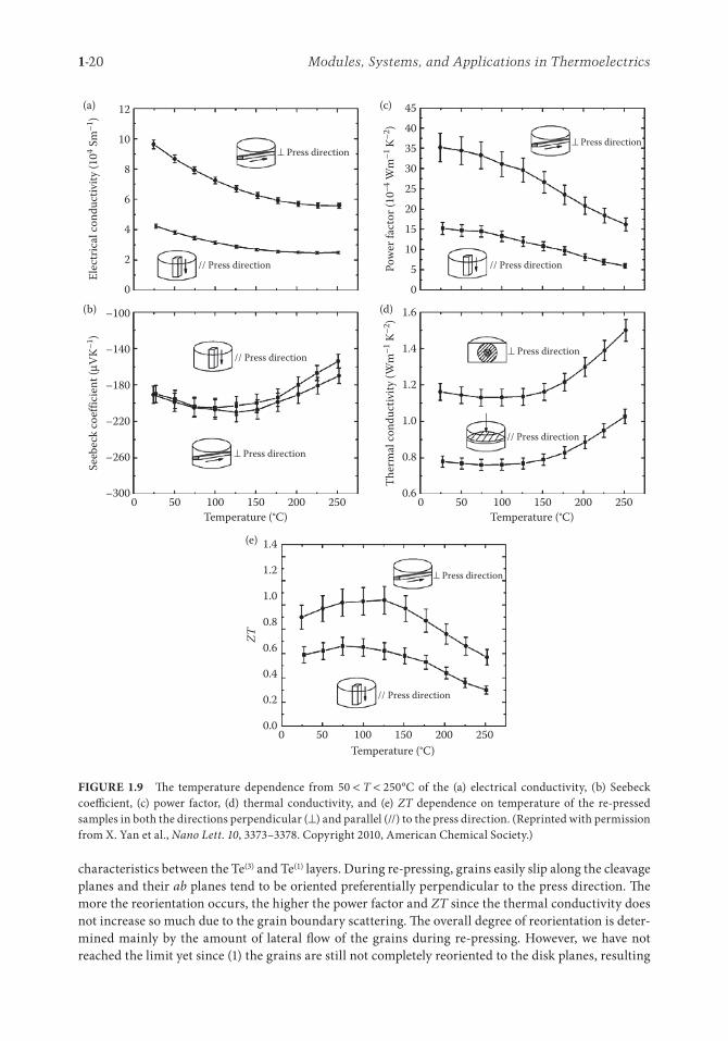
1-20 Modules, Systems, and Applications in Thermoelectrics
characteristics between the Te(3) and Te(1) layers. During re-pressing, grains easily slip along the cleavage planes and their ab planes tend to be oriented preferentially perpendicular to the press direction. �e more the reorientation occurs, the higher the power factor and ZT since the thermal conductivity does not increase so much due to the grain boundary scattering. �e overall degree of reorientation is deter-mined mainly by the amount of lateral ¡ow of the grains during re-pressing. However, we have not reached the limit yet since (1) the grains are still not completely reoriented to the disk planes, resulting
0.6
ZT
1.4
1.2
(b) (d)
(c)(a)
(e)
1.0
0.8
0.6
0.4
0.2
0.00 50 100
Temperature (°C)150 200 250
0 50 100Temperature (°C)
150 200 250 0 50 100Temperature (°C)
150 200 250
0.8
1.0
1.2
1.4
1.6
0
105
15202530
45
3540
12
10
8
6
4
2
0
// Press direction
Elec
tric
al co
nduc
tivity
(104 S
m–1
)
Ther
mal
cond
uctiv
ity (W
m–1
K–2
)Po
wer
fact
or (1
0–4 W
m–1
K–2)
Seeb
eck
coef
ficie
nt (μ
VK–1
)
// Press direction
// Press direction
// Press direction
// Press direction
⊥ Press direction⊥ Press direction
⊥ Press direction
⊥ Press direction
⊥ Press direction
–100
–180
–140
–220
–260
–300
FIGURE 1.9 �e temperature dependence from 50 < T < 250°C of the (a) electrical conductivity, (b) Seebeck coe´cient, (c) power factor, (d) thermal conductivity, and (e) ZT dependence on temperature of the re-pressed samples in both the directions perpendicular (⊥) and parallel (//) to the press direction. (Reprinted with permission from X. Yan et al., Nano Lett. 10, 3373–3378. Copyright 2010, American Chemical Society.)
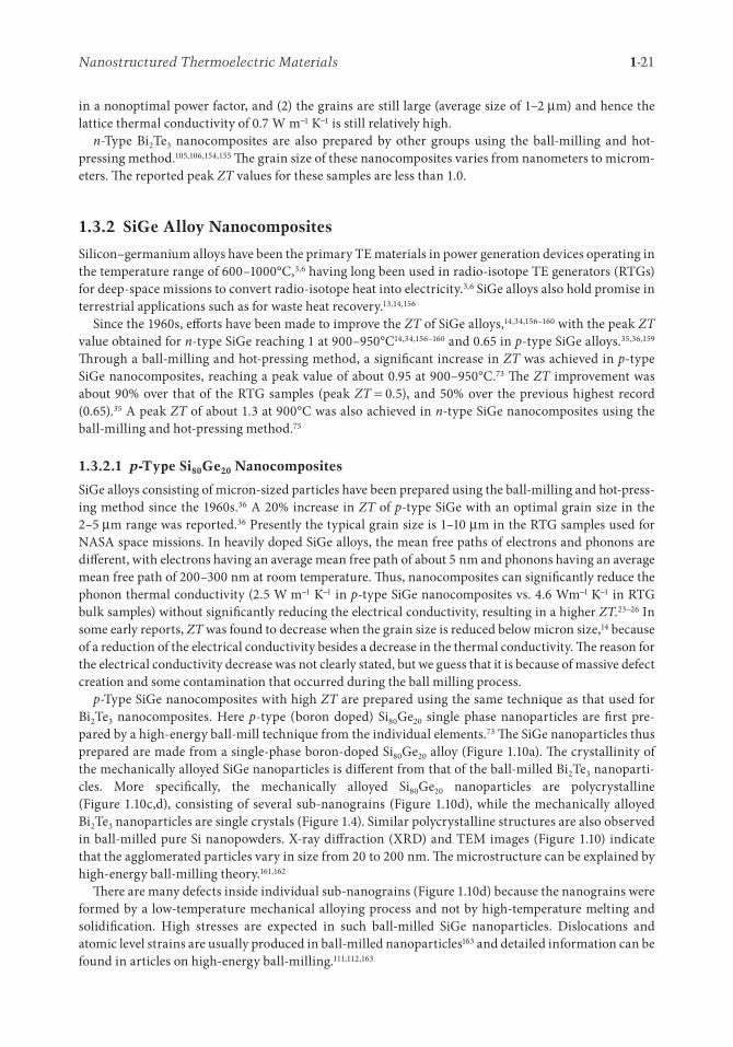
1-21Nanostructured Thermoelectric Materials
in a nonoptimal power factor, and (2) the grains are still large (average size of 1–2 μm) and hence the lattice thermal conductivity of 0.7 W m−1 K−1 is still relatively high.
n-Type Bi2Te3 nanocomposites are also prepared by other groups using the ball-milling and hot-pressing method.105,106,154,155 �e grain size of these nanocomposites varies from nanometers to microm-eters. �e reported peak ZT values for these samples are less than 1.0.
1.3.2 SiGe Alloy Nanocomposites
Silicon–germanium alloys have been the primary TE materials in power generation devices operating in the temperature range of 600–1000°C,3,6 having long been used in radio-isotope TE generators (RTGs) for deep-space missions to convert radio-isotope heat into electricity.3,6 SiGe alloys also hold promise in terrestrial applications such as for waste heat recovery.13,14,156
Since the 1960s, e¤orts have been made to improve the ZT of SiGe alloys,14,34,156–160 with the peak ZT value obtained for n-type SiGe reaching 1 at 900–950°C14,34,156–160 and 0.65 in p-type SiGe alloys.35,36,159 �rough a ball-milling and hot-pressing method, a signi�cant increase in ZT was achieved in p-type SiGe nanocomposites, reaching a peak value of about 0.95 at 900–950°C.73 �e ZT improvement was about 90% over that of the RTG samples (peak ZT = 0.5), and 50% over the previous highest record (0.65).35 A peak ZT of about 1.3 at 900°C was also achieved in n-type SiGe nanocomposites using the ball-milling and hot-pressing method.75
1.3.2.1 p-Type Si80Ge20 Nanocomposites
SiGe alloys consisting of micron-sized particles have been prepared using the ball-milling and hot-press-ing method since the 1960s.36 A 20% increase in ZT of p-type SiGe with an optimal grain size in the 2–5 μm range was reported.36 Presently the typical grain size is 1–10 μm in the RTG samples used for NASA space missions. In heavily doped SiGe alloys, the mean free paths of electrons and phonons are di¤erent, with electrons having an average mean free path of about 5 nm and phonons having an average mean free path of 200–300 nm at room temperature. �us, nanocomposites can signi�cantly reduce the phonon thermal conductivity (2.5 W m−1 K−1 in p-type SiGe nanocomposites vs. 4.6 Wm−1 K−1 in RTG bulk samples) without signi�cantly reducing the electrical conductivity, resulting in a higher ZT.23−26 In some early reports, ZT was found to decrease when the grain size is reduced below micron size,14 because of a reduction of the electrical conductivity besides a decrease in the thermal conductivity. �e reason for the electrical conductivity decrease was not clearly stated, but we guess that it is because of massive defect creation and some contamination that occurred during the ball milling process.
p-Type SiGe nanocomposites with high ZT are prepared using the same technique as that used for Bi2Te3 nanocomposites. Here p-type (boron doped) Si80Ge20 single phase nanoparticles are �rst pre-pared by a high-energy ball-mill technique from the individual elements.73 �e SiGe nanoparticles thus prepared are made from a single-phase boron-doped Si80Ge20 alloy (Figure 1.10a). �e crystallinity of the mechanically alloyed SiGe nanoparticles is di¤erent from that of the ball-milled Bi2Te3 nanoparti-cles. More speci�cally, the mechanically alloyed Si80Ge20 nanoparticles are polycrystalline (Figure 1.10c,d), consisting of several sub-nanograins (Figure 1.10d), while the mechanically alloyed Bi2Te3 nanoparticles are single crystals (Figure 1.4). Similar polycrystalline structures are also observed in ball-milled pure Si nanopowders. X-ray di¤raction (XRD) and TEM images (Figure 1.10) indicate that the agglomerated particles vary in size from 20 to 200 nm. �e microstructure can be explained by high-energy ball-milling theory.161,162
�ere are many defects inside individual sub-nanograins (Figure 1.10d) because the nanograins were formed by a low-temperature mechanical alloying process and not by high-temperature melting and solidi�cation. High stresses are expected in such ball-milled SiGe nanoparticles. Dislocations and atomic level strains are usually produced in ball-milled nanoparticles163 and detailed information can be found in articles on high-energy ball-milling.111,112,163
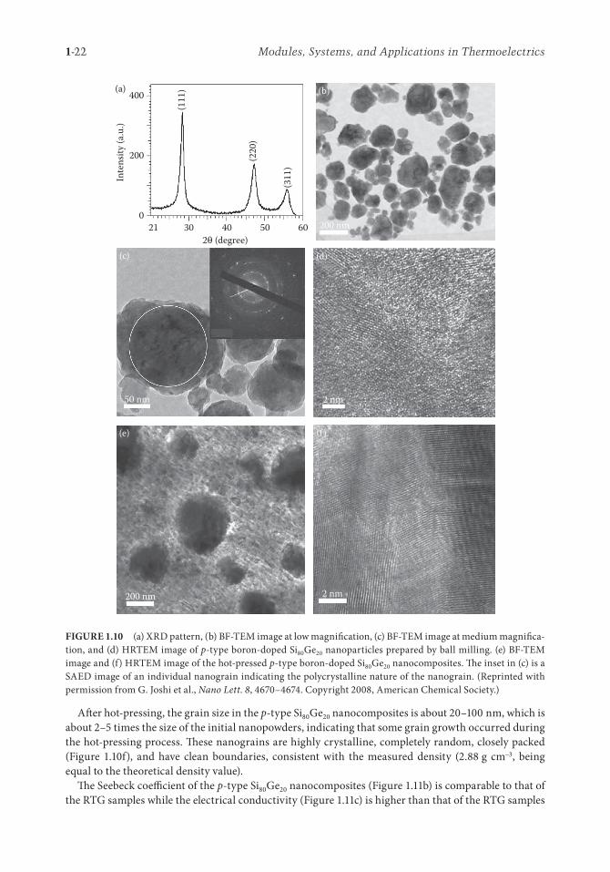
1-22 Modules, Systems, and Applications in Thermoelectrics
A¸er hot-pressing, the grain size in the p-type Si80Ge20 nanocomposites is about 20–100 nm, which is about 2–5 times the size of the initial nanopowders, indicating that some grain growth occurred during the hot-pressing process. �ese nanograins are highly crystalline, completely random, closely packed (Figure 1.10f), and have clean boundaries, consistent with the measured density (2.88 g cm−3, being equal to the theoretical density value).
�e Seebeck coe´cient of the p-type Si80Ge20 nanocomposites (Figure 1.11b) is comparable to that of the RTG samples while the electrical conductivity (Figure 1.11c) is higher than that of the RTG samples
(c)
50 nm
2 nm
2 nm
(d)
(f )(e)
200 nm
200 nm
(b)400
200
021 30 40 50 60
(a)
2θ (degree)
Inte
nsity
(a.u
.)
(111
)
(220
)
(311
)
FIGURE 1.10 (a) XRD pattern, (b) BF-TEM image at low magni�cation, (c) BF-TEM image at medium magni�ca-tion, and (d) HRTEM image of p-type boron-doped Si80Ge20 nanoparticles prepared by ball milling. (e) BF-TEM image and (f) HRTEM image of the hot-pressed p-type boron-doped Si80Ge20 nanocomposites. �e inset in (c) is a SAED image of an individual nanograin indicating the polycrystalline nature of the nanograin. (Reprinted with permission from G. Joshi et al., Nano Lett. 8, 4670–4674. Copyright 2008, American Chemical Society.)
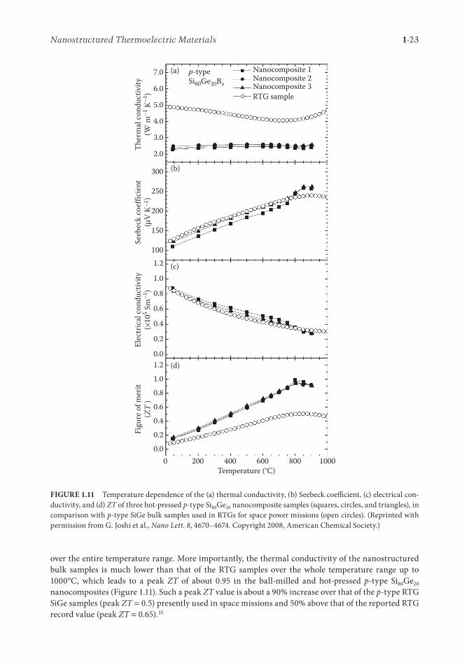
1-23Nanostructured Thermoelectric Materials
over the entire temperature range. More importantly, the thermal conductivity of the nanostructured bulk samples is much lower than that of the RTG samples over the whole temperature range up to 1000°C, which leads to a peak ZT of about 0.95 in the ball-milled and hot-pressed p-type Si80Ge20 nanocomposites (Figure 1.11). Such a peak ZT value is about a 90% increase over that of the p-type RTG SiGe samples (peak ZT = 0.5) presently used in space missions and 50% above that of the reported RTG record value (peak ZT = 0.65).35
00.0
0.2
0.4
0.6
0.8
1.0
1.20.0
0.2
0.4
0.6
0.8
1.0
1.2100
150
200
250
300
2.0
3.0
4.0
5.0
6.0
7.0 (a)
(b)
(c)
(d)
p-type Nanocomposite 1Nanocomposite 2Nanocomposite 3RTG sample
Ther
mal
cond
uctiv
ity(W
m–1
K–1
)Se
ebec
k co
effic
ient
(μV
K–1 )
Elec
tric
al co
nduc
tivity
(×10
5 Sm
–1)
Figu
re o
f mer
it (Z
T )
Si80Ge20Bx
200 400 600 800 1000Temperature (°C)
FIGURE 1.11 Temperature dependence of the (a) thermal conductivity, (b) Seebeck coe´cient, (c) electrical con-ductivity, and (d) ZT of three hot-pressed p-type Si80Ge20 nanocomposite samples (squares, circles, and triangles), in comparison with p-type SiGe bulk samples used in RTGs for space power missions (open circles). (Reprinted with permission from G. Joshi et al., Nano Lett. 8, 4670–4674. Copyright 2008, American Chemical Society.)
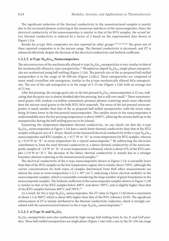
1-24 Modules, Systems, and Applications in Thermoelectrics
�e signi�cant reduction of the thermal conductivity in the nanostructured samples is mainly due to the increased phonon scattering at the numerous interfaces of the nanocomposites. Since the electrical conductivity of the nanocomposites is similar to that of the RTG samples, the actual lat-tice thermal conductivity is reduced by a factor of 2 based on the experimental data shown in Figure 1.11a.
Results for p-type SiGe composites are also reported by other groups.120,124,126,164 �e grain size of these reported composites is in the micron range. �e thermal conductivity is decreased, and ZT is enhanced e¤ectively despite the decrease of the electrical conductivity and Seebeck coe´cient.
1.3.2.2 n-Type Si80Ge20 Nanocomposites
�e microstructure of the mechanically alloyed n-type Si80Ge20 nanoparticles is very similar to that of the mechanically alloyed p-type nanoparticles.75 Phosphorus-doped Si80Ge20 single phase nanoparti-cles are synthesized using ball-milling (Figure 1.12a). �e particle size of the as-prepared ball-milled nanopowders is in the range of 30–200 nm (Figure 1.12b,c). �ese nanoparticles are composed of many small crystalline sub-nanograins, similar to the p-type mechanically alloyed SiGe nanoparti-cles. �e size of the sub-nanograins is in the range of 5–15 nm (Figure 1.12d) with an average size of 12 nm.
A¸er hot pressing, the average grain size in the hot-pressed Si80Ge20 nanocomposites is 22 nm, indi-cating that the grain size is almost doubled a¸er hot pressing, but is still very small.73 �ese nanometer-sized grains with random crystalline orientations promote phonon scattering much more e¤ectively than the micron-sized grains in the bulk RTG SiGe materials. �e stress of the hot-pressed nanocom-posites is much smaller than that of the as-prepared ball-milled nanoparticles, with the strain value being 10 times lower in the hot-pressed nanocomposites. �is smaller strain in the nanocomposites is understandable since the hot-pressing temperature is above 1000°C, allowing the stresses built up in the nanoparticles during the ball-milling process to be relaxed.
Examining the temperature-dependent thermal conductivity, we can clearly see that the n-type Si80Ge20 nanocomposites in Figure 1.13a have a much lower thermal conductivity than that of the RTG samples with grain size of 1–10 μm. Based on the measured electrical conductivity of the n-type Si80Ge20 nanocomposites and RTG samples, κe = 0.77 W m−1 K−1 at room temperature for RTG samples, whereas κe = 0.55 W m−1 K−1 at room temperature for a typical nanocomposite.75 By subtracting the electronic contribution κe from the total thermal conductivity κ, a lattice thermal conductivity of the nanocom-posite samples of ~1.8 W m−1 K−1 at room temperature is obtained, which is about 47% of the RTG sam-ples (~3.8 W m−1 K−1). �e decrease of the lattice thermal conductivity is mainly due to a stronger boundary phonon scattering in the nanostructured samples.75
�e electrical conductivity of the n-type nanocomposites shown in Figure 1.13c is normally lower than that of the RTG samples in the low-temperature region, but is similar above 750°C, although the carrier concentrations for both types of samples determined from Hall e¤ect measurements are almost the same at room temperature (~2.2 × 1020 cm−3), indicating a lower electron mobility in the nanocomposite samples, which is reasonable considering the large number of grain boundaries in the nanocomposite samples. �e Seebeck coe´cient of the nanocomposite samples shown in Figure 1.13b is similar to that of the RTG samples below 400°C and above 700°C, and is slightly higher than that of the RTG samples between 400°C and 700°C.75
As a result, for the n-type Si80Ge20 nanocomposites, the ZT value in Figure 1.13d shows a maximum of about 1.3 at 900°C which is about 40% higher than that of the RTG reference (0.93). �e signi�cant enhancement of ZT is mainly attributed to the thermal conductivity reduction, which is strongly cor-related with the nanostructural features in the n-type Si80Ge20 nanocomposites.75
1.3.2.3 n-Type Si and Si95Ge5
Si95Ge5 nanoparticles were also synthesized by high-energy ball-milling from Si, Ge, P, and GaP pow-ders. �ese ball-milled nanoparticles are single phase (Figure 1.14a) with a size in the 20–150 nm range
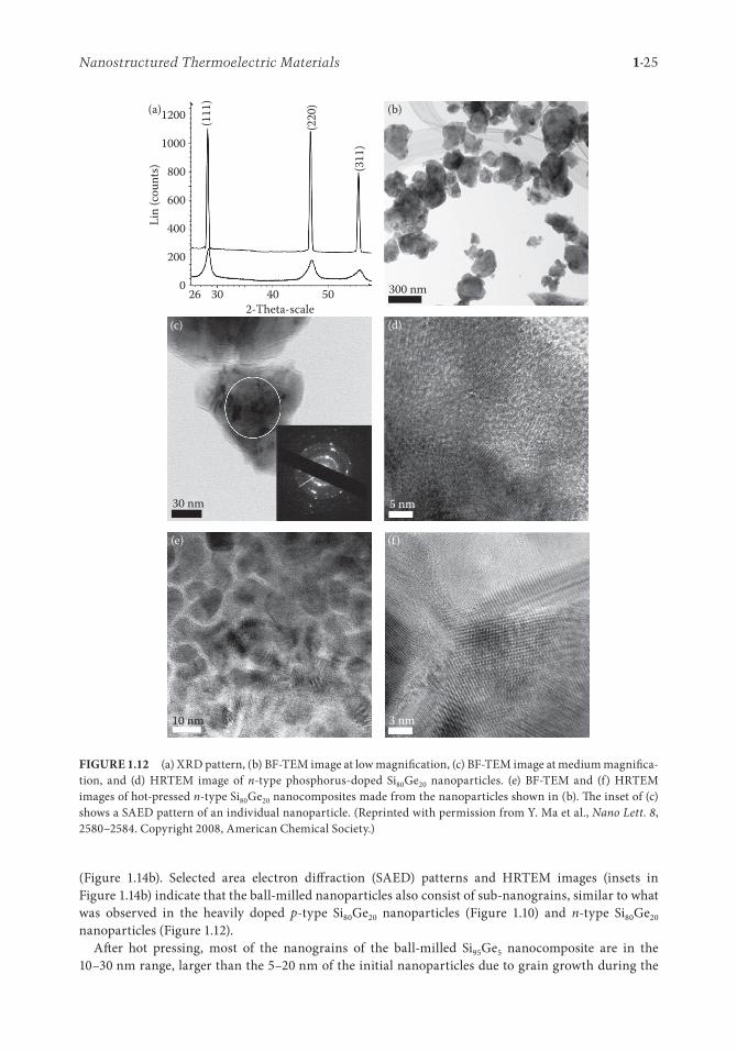
1-25Nanostructured Thermoelectric Materials
(Figure 1.14b). Selected area electron di¤raction (SAED) patterns and HRTEM images (insets in Figure 1.14b) indicate that the ball-milled nanoparticles also consist of sub-nanograins, similar to what was observed in the heavily doped p-type Si80Ge20 nanoparticles (Figure 1.10) and n-type Si80Ge20 nanoparticles (Figure 1.12).
A¸er hot pressing, most of the nanograins of the ball-milled Si95Ge5 nanocomposite are in the 10–30 nm range, larger than the 5–20 nm of the initial nanoparticles due to grain growth during the
(c)
30 nm
3 nm
5 nm
(d)
(f )(e)
300 nm
10 nm
(b)1200
1000
800
600
400
200
026 30 40 50
(a)
2-Theta-scale
Lin
(cou
nts)
(111
)
(220
)
(311
)
FIGURE 1.12 (a) XRD pattern, (b) BF-TEM image at low magni�cation, (c) BF-TEM image at medium magni�ca-tion, and (d) HRTEM image of n-type phosphorus-doped Si80Ge20 nanoparticles. (e) BF-TEM and (f) HRTEM images of hot-pressed n-type Si80Ge20 nanocomposites made from the nanoparticles shown in (b). �e inset of (c) shows a SAED pattern of an individual nanoparticle. (Reprinted with permission from Y. Ma et al., Nano Lett. 8, 2580–2584. Copyright 2008, American Chemical Society.)
1-26 Modules, Systems, and Applications in Thermoelectrics
hot-pressing process. �e nanograins are highly crystalline and randomly oriented a¸er hot pressing (Figure 1.14d).
Figure 1.15 shows the comparative TE property measurement results for the nanostructured Si, Si95Ge5 nanocomposite, bulk Si, and bulk Si80Ge20 RTG alloy samples. Both the nanostructured Si and the nanostructured Si95Ge5 samples show a higher electrical conductivity (Figure 1.15a) but a lower absolute Seebeck coe´cient (Figure 1.15b) than that of the bulk Si80Ge20 RTG sample. �is is mainly
00.0
0.2
0.4
0.6
0.8
1.0
1.4
1.2
0.4
0.6
0.8
1.0
1.2
–300
–250
–200
–150
–50
–100
2.0
3.0
4.0
5.0
6.0 (a)
(b)
(c)
(d)
n-type Nanocomposite 1Nanocomposite 2Nanocomposite 3RTG sample
Ther
mal
cond
uctiv
ity(W
m–1
K–1
)Se
ebec
k co
effic
ient
(μV
K–1)
Elec
tric
al co
nduc
tivity
(×10
5 Sm
–1)
Figu
re o
f mer
it (Z
T )
Si80Ge20P2
200 400 600 800 1000Temperature (°C)
FIGURE 1.13 Temperature dependence in the range 50 < T < 900°C of the (a) thermal conductivity, (b) Seebeck coe´cient, (c) electrical conductivity, and (d) dimensionless ZT of three hot-pressed n-type Si80Ge20 nanocompos-ite samples (squares, triangles, and circles), in comparison with the RTG reference sample (open circles). (Reprinted with permission from X. W. Wang et al., Appl. Phys. Lett. 93, 193121. Copyright 2008, American Institute of Physics.)
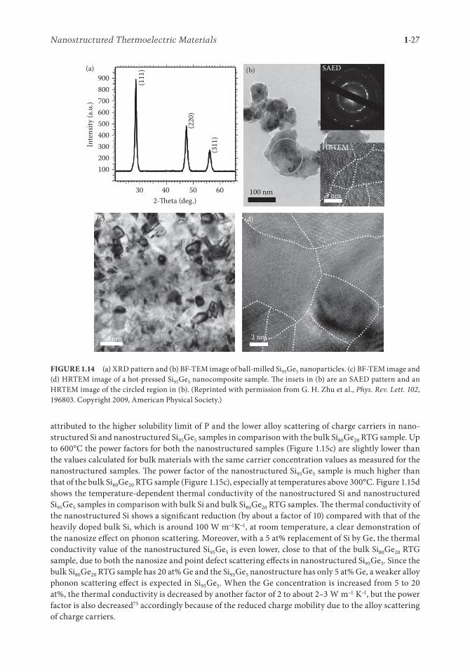
1-27Nanostructured Thermoelectric Materials
attributed to the higher solubility limit of P and the lower alloy scattering of charge carriers in nano-structured Si and nanostructured Si95Ge5 samples in comparison with the bulk Si80Ge20 RTG sample. Up to 600°C the power factors for both the nanostructured samples (Figure 1.15c) are slightly lower than the values calculated for bulk materials with the same carrier concentration values as measured for the nanostructured samples. �e power factor of the nanostructured Si95Ge5 sample is much higher than that of the bulk Si80Ge20 RTG sample (Figure 1.15c), especially at temperatures above 300°C. Figure 1.15d shows the temperature-dependent thermal conductivity of the nanostructured Si and nanostructured Si95Ge5 samples in comparison with bulk Si and bulk Si80Ge20 RTG samples. �e thermal conductivity of the nanostructured Si shows a signi�cant reduction (by about a factor of 10) compared with that of the heavily doped bulk Si, which is around 100 W m−1K−1, at room temperature, a clear demonstration of the nanosize e¤ect on phonon scattering. Moreover, with a 5 at% replacement of Si by Ge, the thermal conductivity value of the nanostructured Si95Ge5 is even lower, close to that of the bulk Si80Ge20 RTG sample, due to both the nanosize and point defect scattering e¤ects in nanostructured Si95Ge5. Since the bulk Si80Ge20 RTG sample has 20 at% Ge and the Si95Ge5 nanostructure has only 5 at% Ge, a weaker alloy phonon scattering e¤ect is expected in Si95Ge5. When the Ge concentration is increased from 5 to 20 at%, the thermal conductivity is decreased by another factor of 2 to about 2–3 W m−1 K−1, but the power factor is also decreased75 accordingly because of the reduced charge mobility due to the alloy scattering of charge carriers.
(c)
50 nm 2 nm
(d)
100 nm 3 nm
HRTEM
SAED(b)
800900
700600500400300200100
6030 40 50
(a)
2-�eta (deg.)
Inte
nsity
(a.u
.)
(111
)
(220
)
(311
)
FIGURE 1.14 (a) XRD pattern and (b) BF-TEM image of ball-milled Si95Ge5 nanoparticles. (c) BF-TEM image and (d) HRTEM image of a hot-pressed Si95Ge5 nanocomposite sample. �e insets in (b) are an SAED pattern and an HRTEM image of the circled region in (b). (Reprinted with permission from G. H. Zhu et al., Phys. Rev. Lett. 102, 196803. Copyright 2009, American Physical Society.)
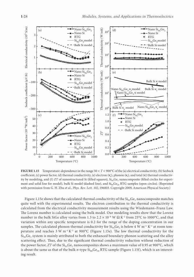
1-28 Modules, Systems, and Applications in Thermoelectrics
Figure 1.15e shows that the calculated thermal conductivity of the Si95Ge5 nanocomposite matches quite well with the experimental results. �e electron contribution to the thermal conductivity is calculated from the electrical conductivity measurement results using the Wiedemann–Franz Law. �e Lorenz number is calculated using the bulk model. Our modeling results show that the Lorenz number in the bulk SiGe alloy varies from 1.3 to 2.2 × 10⁻⁸ W Ω K−2 from 25°C to 1000°C, and that variation within any speci�c temperature is 0.2 for the range of the doping concentration in our samples. �e calculated phonon thermal conductivity for Si95Ge5 is below 4 W m−1 K−1 at room tem-perature and reaches 3 W m−1 K−1 at 900°C (Figure 1.15e). �e low thermal conductivity for the Si95Ge5 system is mainly attributed to both the enhanced boundary phonon scattering and the alloy scattering e¤ect. �us, due to the signi�cant thermal conductivity reduction without reduction of the power factor, ZT of the Si95Ge5 nanocomposites shows a maximum value of 0.95 at 900°C, which is about the same as that of the bulk n-type Si80Ge20 RTG sample (Figure 1.15f), which is an interest-ing result.
0 200 400Temperature (°C)
600 800 10000
Pow
er fa
ctor
(10–4
W/m
K2 )
0
10
20
30
40
50
–300
–200
–100
1
3(a) (d)
(e)(b)
(c) (f )
103
102
101
100
102
101
100
1.2
1.0
0.8
0.6
0.4
0.2
0.0
Nano Si95Ge5
Si95Ge5model
Nano SiRTG
Bulk Si model
Nano Si95Ge5
Si95Ge5model
Nano Si95Ge5 κ1modelNano Si95Ge5 κ model
Nano Si95Ge5 κe model
Nano SiRTG
Bulk Si model
Nano Si95Ge5
Si95Ge5model
Nano SiRTG
Bulk Si model
Nano Si95Ge5
Si95Ge5model
Nano SiRTG
Bulk Si model
Nano Si95Ge5
Si95Ge5model
Nano SiRTG
Bulk Si model
Bulk Si κ model
Bulk Si κ1 model
Bulk Si κe model
2
200 400Temperature (°C)
600 800 1000
Ther
mal
cond
uctiv
ity (W
/mK)
Ther
mal
cond
uctiv
ity (W
/mK)
ZT
Seeb
eck
coeffi
cien
t (μV
/K)
Elec
tric
al co
nduc
tivity
(105 S
/m)
FIGURE 1.15 Temperature-dependence in the range 50 < T < 900°C of the (a) electrical conductivity, (b) Seebeck coe´cient, (c) power factor, (d) thermal conductivity, (e) electron (κe), phonon (κl), and total (κ) thermal conductiv-ity by modeling, and (f) ZT of nanostructured Si (�lled squares), Si95Ge5 nanocomposite (�lled circles for experi-ment and solid line for model), bulk Si model (dashed line), and Si80Ge20 RTG samples (open circles). (Reprinted with permission from G. H. Zhu et al., Phys. Rev. Lett. 102, 196803. Copyright 2009, American Physical Society.)
1-29Nanostructured Thermoelectric Materials
In nanostructured bulk Si, it is reported that the grain boundaries with very high density do not strongly a¤ect the electron mobility but dramatically reduce the lattice thermal conductivity.165 �e combined transport e¤ects produce an increase in the ZT of nanostructured bulk Si by a factor of nearly 3.5, reaching a ZT value of 0.5 at 900°C.
1.3.3 Skutterudite Nanocomposites
Skutterudites have been widely studied for their promising TE properties,166–183 and are regarded as potential candidates for the next-generation TE materials for electrical power generation using either solar energy or waste heat as energy sources. Undoped CoSb3 is p-type with a ZT of about 0.2.128 A¸er doping with rare earth elements, ZT increases to 0.52 at 600 K for n-type bulk crystals.184 A peak ZT value of 0.7 was achieved in n-type (Ni,Co)4Sb12 nanocomposites produced by the ball-milling and hot-pressing method.128
Another remarkable feature of skutterudites is that the cage-like open structure of the compounds can be �lled with foreign atoms acting as phonon rattlers. �e �lled foreign atoms scatter phonons strongly and drastically reduce the thermal conductivity of the skutterudite compounds.166–183 With various kinds of atoms �lling the cages, an increased ZT can be achieved in RxCo4Sb12 (R = Ce,185 La,186 Ca,187 Ba,188 and Yb115,189,190). For example, Yb �lled n-type Yb0.19Co4Sb12 with a peak ZT close to 1 at 373°C189 and Yb0.15Co4Sb12 with a peak ZT of about 0.7 at 400°C 190 have been reported. �e peak ZT of YbxCo4Sb12 nanocomposites made from the ball-milling and hot-pressing method was increased to 1.2.127
1.3.3.1 n-Type YbxCo4Sb12 Nanocomposites
We have tried to obtain YbxCo4Sb12 nanopowders by ball milling from elements. However, unlike the Bi2Te3 and SiGe systems, only a small portion of the ball-milled nanopowders are mechanically alloyed a¸er high-energy ball milling, regardless of the ball-milling time. �e same phenomenon is also observed in other skutterudites, such as CoSb3,191 (La,Ni,Co)4Sb12,192 FexCo4Co12,117,191 Co(Sb,Te)3,109 and FeCo3Sb12,193 and in other material systems such as the Ag0.8Pb18+xSbTe20 system.107 �is phenomenon is common in mechanical alloying. For some TE compounds, like FeSi2, the ball-milling process does not mechanically alloy Fe and Si elements.194 However, the ball-milling process does mix the elements uni-formly at the nanometer scale, facilitating the alloying via a chemical reaction during the hot-pressing process.
A¸er the hot pressing, the nanopowders are completely transformed into a single-phase skutterudite. �e average grain size is about 200–500 nm (Figure 1.16). �ere are two types of nanograins in the skut-terudite nanocomposites: larger ones of about 1 μm in a bar shape (in the middle of Figure 1.16a), and smaller ones of about 200–500 nm in a spherical shape. �e larger ones could grow from the mechani-cally alloyed small particles while the smaller ones could form from un-alloyed powders.128 Both types of nanograins are well crystallized with clear facets. �e crystallized grains are closely packed, implying a high density, consistent with the theoretical density of Yb0.35Co4Sb12 (7.6 g cm−3).
All the nanograins in the nanocomposites are well crystallized, and the large-angle grain boundaries in Figure 1.16b are clean. �e excellent crystallinity and clean grain boundaries are needed to achieve good electrical transport properties, whereas the large-angle grain boundaries also bene�t phonon scattering.
A series of YbxCo4Sb12 (x = 0.3, 0.35, 0.4, 0.5, and 1.0) nanostructured samples were prepared by ball milling and hot pressing. Of these, Yb0.35Co4Sb12 has an optimized lowest thermal conductivity with a minimum value of 2.7 W m-1 K-1, which leads to the highest observed ZT value among all the samples.127 Below we focus on the Yb0.35Co4Sb12 nanostructured sample.
�e TE properties of Yb0.35Co4Sb12 are next compared with other reported properties of nanocom-posites prepared by the ball-milling and hot-pressing method. �e nanocomposites produced here show a much higher electrical conductivity than those reported previously,115,189 presumably due to the large electron doping e¤ect from the high Yb concentration. �e thermal conductivity of the
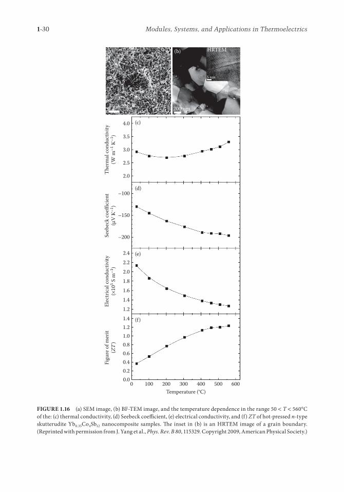
1-30 Modules, Systems, and Applications in Thermoelectrics
0 100 200 300 400 500 600Temperature (°C)
Ther
mal
cond
uctiv
ity(W
m–1
K–1
)Se
ebec
k co
effic
ient
(μV
K–1)
Elec
tric
al co
nduc
tivity
(×10
5 S m
–1)
Figu
re o
f mer
it (Z
T )
0.00.20.40.60.81.0
1.41.2
1.21.41.61.82.02.22.4
–200
–150
–100
2.0
2.5
3.0
3.5
4.0
1 μm 200 nm
(b) HRTEM
5 nm
(a)
(c)
(d)
(e)
(f )
FIGURE 1.16 (a) SEM image, (b) BF-TEM image, and the temperature dependence in the range 50 < T < 560°C of the: (c) thermal conductivity, (d) Seebeck coe´cient, (e) electrical conductivity, and (f) ZT of hot-pressed n-type skutterudite Yb0.35Co4Sb12 nanocomposite samples. �e inset in (b) is an HRTEM image of a grain boundary. (Reprinted with permission from J. Yang et al., Phys. Rev. B 80, 115329. Copyright 2009, American Physical Society.)
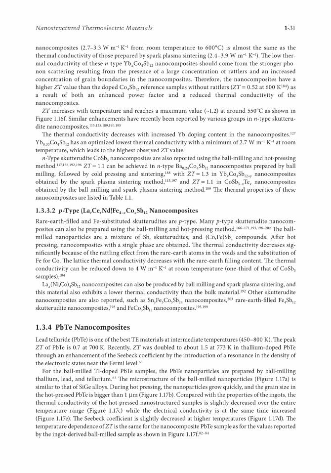
1-31Nanostructured Thermoelectric Materials
nanocomposites (2.7–3.3 W m−1 K−1 from room temperature to 600°C) is almost the same as the thermal conductivity of those prepared by spark plasma sintering (2.4–3.9 W m−1 K−1). �e low ther-mal conductivity of these n-type YbxCo4Sb12 nanocomposites should come from the stronger pho-non scattering resulting from the presence of a large concentration of rattlers and an increased concentration of grain boundaries in the nanocomposites. �erefore, the nanocomposites have a higher ZT value than the doped Co4Sb12 reference samples without rattlers (ZT = 0.52 at 600 K184) as a result of both an enhanced power factor and a reduced thermal conductivity of the nanocomposites.
ZT increases with temperature and reaches a maximum value (~1.2) at around 550°C as shown in Figure 1.16f. Similar enhancements have recently been reported by various groups in n-type skutteru-dite nanocomposites.115,128,189,190,195
�e thermal conductivity decreases with increased Yb doping content in the nanocomposites.127 Yb0.35Co4Sb12 has an optimized lowest thermal conductivity with a minimum of 2.7 W m−1 K−1 at room temperature, which leads to the highest observed ZT value.
n-Type skutterudite CoSb3 nanocomposites are also reported using the ball-milling and hot-pressing method.117,138,192,196 ZT = 1.1 can be achieved in n-type Ba0.24Co4Sb12 nanocomposites prepared by ball milling, followed by cold pressing and sintering,188 with ZT = 1.3 in YbxCo4Sb12+y nanocomposites obtained by the spark plasma sintering method,115,197 and ZT = 1.1 in CoSb3−xTex nanocomposites obtained by the ball milling and spark plasma sintering method.109 �e thermal properties of these nanocomposites are listed in Table 1.1.
1.3.3.2 p-Type (La,Ce,Nd)Fe4–xCoxSb12 Nanocomposites
Rare-earth-�lled and Fe-substituted skutterudites are p-type. Many p-type skutterudite nanocom-posites can also be prepared using the ball-milling and hot-pressing method.166–171,193,198–202 �e ball-milled nanoparticles are a mixture of Sb, skutterudites, and (Co,Fe)Sb2 compounds. A¸er hot pressing, nanocomposites with a single phase are obtained. �e thermal conductivity decreases sig-ni�cantly because of the rattling e¤ect from the rare-earth atoms in the voids and the substitution of Fe for Co. �e lattice thermal conductivity decreases with the rare-earth �lling content. �e thermal conductivity can be reduced down to 4 W m−1 K−1 at room temperature (one-third of that of CoSb3 samples).184
Lax(Ni,Co)4Sb12 nanocomposites can also be produced by ball milling and spark plasma sintering, and this material also exhibits a lower thermal conductivity than the bulk material.192 Other skutterudite nanocomposites are also reported, such as SnyFe3Co5Sb24 nanocomposites,203 rare-earth-�lled Fe4Sb12 skutterudite nanocomposites,198 and FeCo3Sb12 nanocomposites.193,199
1.3.4 PbTe Nanocomposites
Lead telluride (PbTe) is one of the best TE materials at intermediate temperatures (450–800 K). �e peak ZT of PbTe is 0.7 at 700 K. Recently, ZT was doubled to about 1.5 at 773 K in thallium-doped PbTe through an enhancement of the Seebeck coe´cient by the introduction of a resonance in the density of the electronic states near the Fermi level.63
For the ball-milled Tl-doped PbTe samples, the PbTe nanoparticles are prepared by ball-milling thallium, lead, and tellurium.83 �e microstructure of the ball-milled nanoparticles (Figure 1.17a) is similar to that of SiGe alloys. During hot pressing, the nanoparticles grow quickly, and the grain size in the hot-pressed PbTe is bigger than 1 μm (Figure 1.17b). Compared with the properties of the ingots, the thermal conductivity of the hot-pressed nanostructured samples is slightly decreased over the entire temperature range (Figure 1.17c) while the electrical conductivity is at the same time increased (Figure 1.17e). �e Seebeck coe´cient is slightly decreased at higher temperatures (Figure 1.17d). �e temperature dependence of ZT is the same for the nanocomposite PbTe sample as for the values reported by the ingot-derived ball-milled sample as shown in Figure 1.17f.82–84
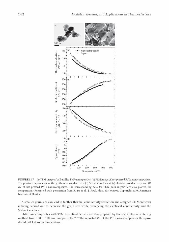
1-32 Modules, Systems, and Applications in Thermoelectrics
A smaller grain size can lead to further thermal conductivity reduction and a higher ZT. More work is being carried out to decrease the grain size while preserving the electrical conductivity and the Seebeck coe´cient.
PbTe nanocomposites with 95% theoretical density are also prepared by the spark plasma sintering method from 100 to 150 nm nanoparticles.98,99 �e reported ZT of the PbTe nanocomposites thus pro-duced is 0.1 at room temperature.
0 100 200 300 400 5000.00.20.40.60.81.0
1.41.6
1.2
2.0
3.0
4.0
5.0100
150
200
250
300
350
2.0
2.5
1.0
1.5
5 μm200 nm
(b)(a)
(c) NanocompositesIngots
(d)
(e)
(f )
Temperature (°C)
Ther
mal
cond
uctiv
ity(W
m–1
K–1
)Se
ebec
k co
effic
ient
(μV
K–1)
Elec
tric
al co
nduc
tivity
(×10
5 S m
–1)
Figu
re o
f mer
it (Z
T )
FIGURE 1.17 (a) TEM image of ball-milled PbTe nanopowder. (b) SEM image of hot-pressed PbTe nanocomposites. Temperature dependence of the (c) thermal conductivity, (d) Seebeck coe´cient, (e) electrical conductivity, and (f) ZT of hot-pressed PbTe nanocomposites. �e corresponding data for PbTe bulk ingots83 are also plotted for comparison. (Reprinted with permission from B. Yu et al., J. Appl. Phys. 108, 016104. Copyright 2010, American Institute of Physics.)
1-33Nanostructured Thermoelectric Materials
1.3.5 Half-Heusler Nanocomposites
�e potential of half-Heusler alloys for high-temperature TE power generation has been discussed.204,205 Half-Heuslers have the cubic MgAgAs type of structure, forming three interpenetrating face-centered-cubic (fcc) sublattices and one vacant sublattice.206 Until recently the reported p-type half-Heusler alloys are mostly based on the formula MCoSb, where M is Ti, Zr, or Hf.207–210 �e high substitutability of the three lattice sites (M, Co, and Sb) provides many opportunities for tuning the electronic and lattice properties of the half-Heuslers. �rough partial elemental substitution, the large lattice thermal con-ductivity of half-Heusler compounds is expected to be greatly reduced due to mass ¡uctuation and strain �eld e¤ects.207–210 However, the thermal conductivity of p-type half-Heusler alloys reported so far still remains very high relatively (higher than 4 W m−1 K−1),207–210 which prevents ZT from reaching a meaningful value for a TE material. �e highest ZT of about 0.5 in p-type Zr0.5Hf0.5CoSb0.8Sn0.2 was achieved at 1000 K with a thermal conductivity of 4.1 W m−1 K−1 at 300 K and 3.6 W m−1 K−1 at 1000 K.211 Such a thermal conductivity is still very high due mainly to the relatively large contribution of the lat-tice thermal conductivity. Besides alloy scattering via partial elemental substitution, boundary scatter-ing can be introduced to further reduce the thermal conductivity.212 Even though ball milling was attempted to reduce the thermal conductivity by decreasing the average grain size, the ZT improve-ment was minimal due to the still too large average grain size of at least 1 micrometer.213–215 Based on our success in achieving a grain size much smaller than 1 μm in a number of materials by ball milling and hot pressing,72–76,127 we have succeeded in achieving grain sizes smaller than 200 nm in p-type half-Heusler samples with the composition of Zr0.5Hf0.5CoSb0.8Sn0.2 by ball milling the alloyed ingot into nanopowders and then hot pressing them into dense bulk samples, resulting in a simultaneous increase in the Seebeck coe´cient and a signi�cant decrease in the thermal conductivity, which led to a 60% increase in the peak ZT from 0.5 to 0.8 at 700°C.216
In a typical experiment, the alloyed ingot with the composition of Zr0.5Hf0.5CoSb0.8Sn0.2 was loaded into a jar with grinding balls and then subjected to a mechanical ball milling process.216
Figure 1.18 shows the TEM images of the ball-milled nanopowders. �e low (Figure 1.18a) and medium (Figure 1.18b) magni�cation TEM images show that the average cluster size of the nanopow-ders ranges from 20 to 500 nm. However, those big clusters are actually agglomerates of many much smaller crystalline nanograins, which is con�rmed by the corresponding selected area electron dif-fraction (SAED) patterns (Figure 1.18c) obtained inside a single cluster (Figure 1.18b). �e high-resolution TEM image (Figure 1.18d) shows that the sizes of the small grains are in the range of 5–10 nm.
Figure 1.19 displays the TEM images of the as-pressed bulk samples pressed from the ball-milled powder. �e low-magni�cation TEM image is presented in Figure 1.19a, from which we can see that the grain sizes are in the range of 50–300 nm with an estimated average size being about 100–200 nm. �erefore, there is a signi�cant grain growth during the hot-pressing process. �e SAED pattern (inset of Figure 1.19a) of each individual grain indicates that the individual grains are single crystalline. �e high-resolution TEM image (Figure 1.19b) demonstrates the good crystallinity inside each individual grain. Figure 1.19c shows one nanodot embedded inside the matrix. Such dots are commonly observed in most of the grains. �e compositions of both the nanodot and its surrounding areas are checked by energy-dispersive x-ray spectroscopy (EDS), showing Hf-rich and Co-de�cient regions for the nanodot. Another feature pertaining to our sample is that small grains (~30 nm) are also common (Figure 1.19d), which have similar composition as the surrounding bigger grains determined by EDS. We suspect that the nonuniformity in both the grain sizes and the compositions all contribute to the reduction of the thermal conductivity.
�e temperature-dependent TE properties of the hot-pressed Zr0.5Hf0.5CoSb0.8Sb0.2 bulk samples in comparison with that of the ingot are plotted in Figure 1.20. For all of the samples examined, the tem-perature dependence of the electrical conductivity was found to exhibit semimetallic or degenerate semiconductor behavior (Figure 1.20a). Speci�cally, the electrical conductivities of all the ball-milled
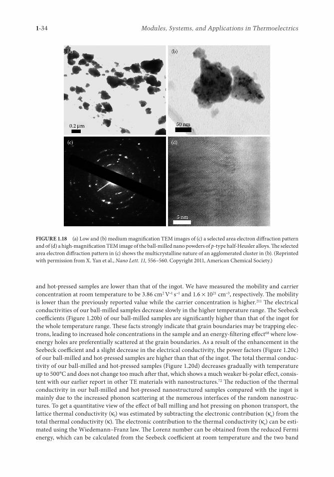
1-34 Modules, Systems, and Applications in Thermoelectrics
and hot-pressed samples are lower than that of the ingot. We have measured the mobility and carrier concentration at room temperature to be 3.86 cm2 V−1 s−1 and 1.6 × 1021 cm−3, respectively. �e mobility is lower than the previously reported value while the carrier concentration is higher.211 �e electrical conductivities of our ball-milled samples decrease slowly in the higher temperature range. �e Seebeck coe´cients (Figure 1.20b) of our ball-milled samples are signi�cantly higher than that of the ingot for the whole temperature range. �ese facts strongly indicate that grain boundaries may be trapping elec-trons, leading to increased hole concentrations in the sample and an energy-�ltering e¤ect68 where low-energy holes are preferentially scattered at the grain boundaries. As a result of the enhancement in the Seebeck coe´cient and a slight decrease in the electrical conductivity, the power factors (Figure 1.20c) of our ball-milled and hot-pressed samples are higher than that of the ingot. �e total thermal conduc-tivity of our ball-milled and hot-pressed samples (Figure 1.20d) decreases gradually with temperature up to 500°C and does not change too much a¸er that, which shows a much weaker bi-polar e¤ect, consis-tent with our earlier report in other TE materials with nanostructures.72 �e reduction of the thermal conductivity in our ball-milled and hot-pressed nanostructured samples compared with the ingot is mainly due to the increased phonon scattering at the numerous interfaces of the random nanostruc-tures. To get a quantitative view of the e¤ect of ball milling and hot pressing on phonon transport, the lattice thermal conductivity (κl) was estimated by subtracting the electronic contribution (κe) from the total thermal conductivity (κ). �e electronic contribution to the thermal conductivity (κe) can be esti-mated using the Wiedemann–Franz law. �e Lorenz number can be obtained from the reduced Fermi energy, which can be calculated from the Seebeck coe´cient at room temperature and the two band
FIGURE 1.18 (a) Low and (b) medium magni�cation TEM images of (c) a selected area electron di¤raction pattern and of (d) a high-magni�cation TEM image of the ball-milled nano powders of p-type half-Heusler alloys. �e selected area electron di¤raction pattern in (c) shows the multicrystalline nature of an agglomerated cluster in (b). (Reprinted with permission from X. Yan et al., Nano Lett. 11, 556–560. Copyright 2011, American Chemical Society.)
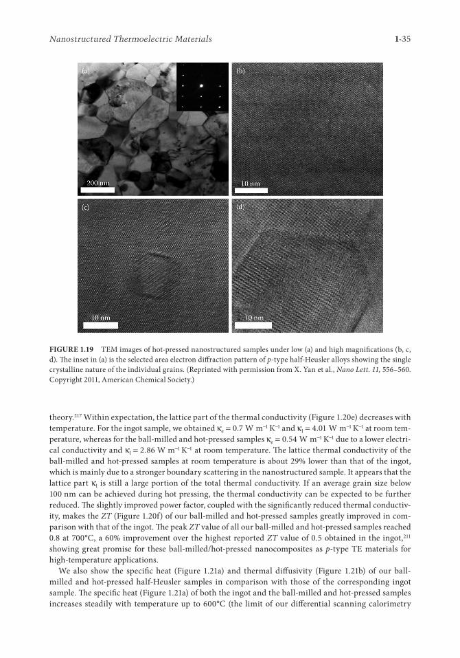
1-35Nanostructured Thermoelectric Materials
theory.217 Within expectation, the lattice part of the thermal conductivity (Figure 1.20e) decreases with temperature. For the ingot sample, we obtained κe = 0.7 W m−1 K−1 and κl = 4.01 W m−1 K−1 at room tem-perature, whereas for the ball-milled and hot-pressed samples κe = 0.54 W m−1 K−1 due to a lower electri-cal conductivity and κl = 2.86 W m−1 K−1 at room temperature. �e lattice thermal conductivity of the ball-milled and hot-pressed samples at room temperature is about 29% lower than that of the ingot, which is mainly due to a stronger boundary scattering in the nanostructured sample. It appears that the lattice part κl is still a large portion of the total thermal conductivity. If an average grain size below 100 nm can be achieved during hot pressing, the thermal conductivity can be expected to be further reduced. �e slightly improved power factor, coupled with the signi�cantly reduced thermal conductiv-ity, makes the ZT (Figure 1.20f) of our ball-milled and hot-pressed samples greatly improved in com-parison with that of the ingot. �e peak ZT value of all our ball-milled and hot-pressed samples reached 0.8 at 700°C, a 60% improvement over the highest reported ZT value of 0.5 obtained in the ingot,211 showing great promise for these ball-milled/hot-pressed nanocomposites as p-type TE materials for high-temperature applications.
We also show the speci�c heat (Figure 1.21a) and thermal di¤usivity (Figure 1.21b) of our ball-milled and hot-pressed half-Heusler samples in comparison with those of the corresponding ingot sample. �e speci�c heat (Figure 1.21a) of both the ingot and the ball-milled and hot-pressed samples increases steadily with temperature up to 600°C (the limit of our di¤erential scanning calorimetry
FIGURE 1.19 TEM images of hot-pressed nanostructured samples under low (a) and high magni�cations (b, c, d). �e inset in (a) is the selected area electron di¤raction pattern of p-type half-Heusler alloys showing the single crystalline nature of the individual grains. (Reprinted with permission from X. Yan et al., Nano Lett. 11, 556–560. Copyright 2011, American Chemical Society.)
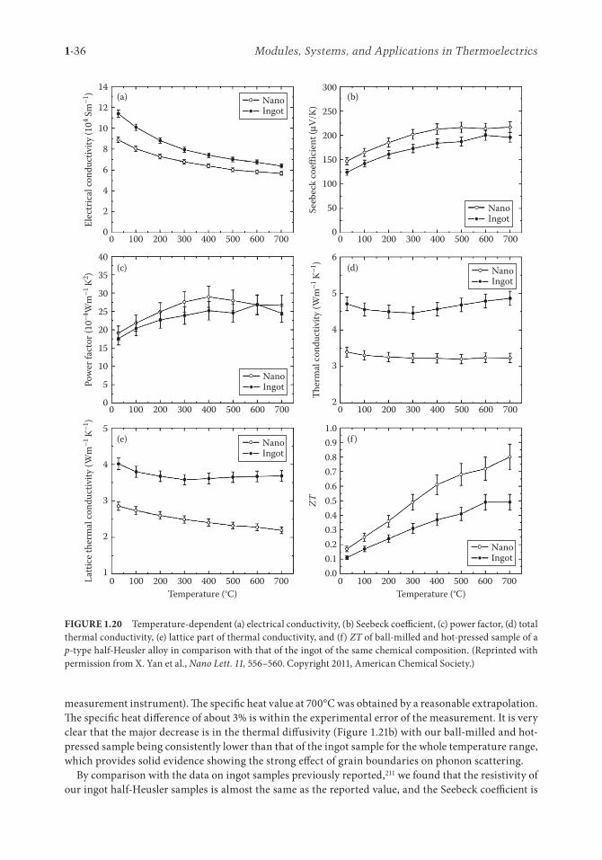
1-36 Modules, Systems, and Applications in Thermoelectrics
measurement instrument). �e speci�c heat value at 700°C was obtained by a reasonable extrapolation. �e speci�c heat di¤erence of about 3% is within the experimental error of the measurement. It is very clear that the major decrease is in the thermal di¤usivity (Figure 1.21b) with our ball-milled and hot-pressed sample being consistently lower than that of the ingot sample for the whole temperature range, which provides solid evidence showing the strong e¤ect of grain boundaries on phonon scattering.
By comparison with the data on ingot samples previously reported,211 we found that the resistivity of our ingot half-Heusler samples is almost the same as the reported value, and the Seebeck coe´cient is
00.00.10.20.30.40.50.60.70.80.91.0
2
3
4
5
6
0
50
100
150
200
250
30014
12
10
8
6
4
2
0
40
35
30
25
20
15
10
5
0
5
4
3
2
1100 200 300 400 500 600 700
0 100 200 300 400 500 600 700
0 100 200 300 400 500 600 7000 100 200 300 400 500 600 700
(e)
(c) (d)
(b)(a)
(f )
0 100 200 300 400 500 600 700
Temperature (°C)0 100 200 300 400 500 600 700
Temperature (°C)
Pow
er fa
ctor
(10–4
Wm
–1 K2 )
Ther
mal
cond
uctiv
ity (W
m–1
K–1)
Latti
ce th
erm
al co
nduc
tivity
(Wm
–1 K–1
)
ZTSe
ebec
k co
effic
ient
(μV/
K)
Elec
tric
al co
nduc
tivity
(104 S
m–1
)
NanoIngot
NanoIngot
NanoIngot
NanoIngot
NanoIngot
NanoIngot
FIGURE 1.20 Temperature-dependent (a) electrical conductivity, (b) Seebeck coe´cient, (c) power factor, (d) total thermal conductivity, (e) lattice part of thermal conductivity, and (f) ZT of ball-milled and hot-pressed sample of a p-type half-Heusler alloy in comparison with that of the ingot of the same chemical composition. (Reprinted with permission from X. Yan et al., Nano Lett. 11, 556–560. Copyright 2011, American Chemical Society.)
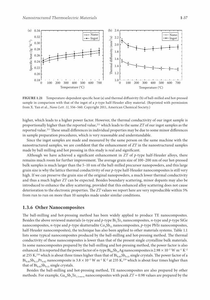
1-37Nanostructured Thermoelectric Materials
higher, which leads to a higher power factor. However, the thermal conductivity of our ingot sample is proportionally higher than the reported value,211 which leads to the same ZT of our ingot samples as the reported value.211 �ese small di¤erences in individual properties may be due to some minor di¤erences in sample preparation procedures, which is very reasonable and understandable.
Since the ingot samples are made and measured by the same person on the same machine with the nanostructured samples, we are con�dent that the enhancement of ZT in the nanostructured samples made by ball milling and hot pressing in this study is real and signi�cant.
Although we have achieved a signi�cant enhancement in ZT of p-type half-Heusler alloys, there remains much room for further improvement. �e average grain size of 100–200 nm of our hot-pressed bulk samples is much larger than the 5–10 nm of the ball-milled precursor nanopowders, and this large grain size is why the lattice thermal conductivity of our p-type half-Heusler nanocomposites is still very high. If we can preserve the grain size of the original nanopowders, a much lower thermal conductivity and thus a much higher ZT can be expected. Besides boundary scattering, minor dopants may also be introduced to enhance the alloy scattering, provided that this enhanced alloy scattering does not cause deterioration to the electronic properties. �e ZT values we report here are very reproducible within 5% from run to run on more than 10 samples made under similar conditions.
1.3.6 Other Nanocomposites
�e ball-milling and hot-pressing method has been widely applied to produce TE nanocomposites. Besides the above reviewed materials (n-type and p-type Bi2Te3 nanocomposites, n-type and p-type SiGe nanocomposites, n-type and p-type skutterudite Co4Sb12 nanocomposites, p-type PbTe nanocomposites, half-Heusler nanocomposites), the technique has also been applied to other materials systems. Table 1.1 lists some typical nanocomposites produced by the ball-milling and hot-pressing method. �e thermal conductivity of these nanocomposites is lower than that of the present single crystalline bulk materials. In some nanocomposites prepared by the ball-milling and hot-pressing method, the power factor is also enhanced. It is reported that the power factor of n-type Bi85Sb14Ag nanocomposites is 2.98 × 10⁻³ W m−1 K−2 at 255 K,218 which is about three times higher than that of Bi0.85Sb0.15 single crystals. �e power factor of a Bi0.85Sb0.13Pr0.02 nanocomposite is 3.8 × 10⁻³ W m−1 K−2 at 235 K,219 which is about four times higher than that of Bi0.85Sb0.15 single crystals.
Besides the ball-milling and hot-pressing method, TE nanocomposites are also prepared by other methods. For example, GamSbnTe1.5+m+n nanocomposites with peak ZT = 0.98 values are prepared by the
01.0
1.2
1.4
1.6
1.8
2.0
2.2
2.4
0.18
0.20
0.22
0.24
0.26
0.28
0.30
0.32
0.34
100 200 300 400 500 600 700
Nano(a) (b)
IngotNanoIngot
Temperature (°C)0 100 200 300 400 500 600 700
Temperature (°C)
Spec
ific h
eat (
Jg–1
K–1)
er
mal
diff
usiv
ity (m
m2 /s
)
FIGURE 1.21 Temperature-dependent speci�c heat (a) and thermal di¤usivity (b) of ball-milled and hot-pressed sample in comparison with that of the ingot of a p-type half-Heusler alloy material. (Reprinted with permission from X. Yan et al., Nano Lett. 11, 556–560. Copyright 2011, American Chemical Society.)
1-38 Modules, Systems, and Applications in Thermoelectrics
spark plasma sintering method from ball-milled nanoparticles.220 �e nanograin size is small (<30 nm). Zn4Sb3 nanocomposites are produced by sintering cold-pressed samples.118 �e thermal conductivity of Ag0.008Pb0.18+xSbTe0.20 nanocomposites decreases by 40% a¸er ball-milling and spark plasma sintering and a peak ZT value of 1.3 was reported for this material at 300°C.107 Bi1−xSbx nanocomposites obtained by a ball-milling and extrusion method showed a thermal conductivity decrease of 75%.101 �ese nano-composites are also listed in Table 1.1.
In all of these TE nanocomposites, the thermal conductivity is decreased. Despite this, ZT is not nec-essarily enhanced, and could even be decreased in these nanocomposites, depending on the change of the electrical conductivity and the Seebeck coe´cient.
To further decrease the thermal conductivity, additional phases have been dispersed into the nano-composites. It is postulated that the addition of second-phase nanoparticles will work as phonon scat-tering centers and further decrease the thermal conductivity. ZnO2 and rare-earth oxides have been added into β-FeSi2 nanocomposites.221 It is reported that the dispersion of Y2O3 nanoparticles doubles the ZT of n-type β-FeSi2 nanocomposites from 0.35 to 0.63 when 2 wt% Y2O3 is added to the material being nanostructured.222 �e thermal conductivity then decreases to 0.7 from 4.5 W m−1 K−1 a¸er the addition of the nanoparticles.
TiB2 has also been dispersed into a β-FeSi2 nanocomposite material using the ball-milling and hot-pressing method.223 However, increasing the TiB2 content (0–30 vol%) results in a decreased power factor and ZT. TiB2 has also been dispersed into B4C nanocomposites using the ball-milling and hot-pressing method.224 B4C works as a TE host. Both the thermal conductivity and the electrical conductivity decrease with increasing TiB2 content from 0 to 25 vol% and ZT also decreases.
BN and WO3 have been dispersed into p-type (Bi,Sb)2Te3 nanocomposites using the ball-milling and hot-pressing method.225 �e thermal conductivity decreases slightly from 1.5 to 1.2 W m−1 K−1 when the volume fraction of BN and WO3 increases from 0 to 7 vol%. ZT decreases with increasing BN and WO3 content because of a rapid decrease of the electrical conductivity.
In all of these nanocomposites with additions of second-phase nanoparticles, the thermal conductiv-ity indeed decreases with increasing volume fraction of the second phase because of enhanced phonon scattering. However, the addition of the second phase also decreases the electrical conductivity and Seebeck coe´cient. ZT usually decreases because of a greater reduction in electrical conductivity and Seebeck coe´cient. In order to increase the ZT of the nanocomposites with the addition of a second-phase material, it is necessary to avoid a decrease of the electrical conductivity and Seebeck coe´cient of the mixture a¸er the addition of a second phase. One possible cause for the decreased electrical con-ductivity and/or Seebeck coe´cient is due to a large band structure mismatch between the added second phase and the host materials, leading to either a too high or too low carrier concentration. Another cause is that the second phase reacts with the host materials to change fundamentally the electronic band structures. It is also possible that these second phases form a percolating conducting phase that signi�cantly changes the transport properties. More work is needed to clarify these mechanisms before this approach can be used successfully.
It is also suggested that an amorphous structure and lattice distortion in the TE materials can con-tribute to a decrease in the thermal conductivity,220 as well as atomic disorder decreasing the thermal conductivity.226 �is is another approach to produce an increase in ZT through introducing amorphous or defect phonon scattering centers. Further investigation into this method for possible enhancement of ZT is expected in the future.
1.4 Phonon Transport in Nanocomposites
Since most nanocomposites to date have achieved their high ZT values by a reduction in lattice thermal conductivity, one might expect that phonon transport in nanocomposites is fairly well understood. However, the situation turns out to be just the opposite. Even in bulk materials, there is much uncertainty regarding the values of key physical parameters and the physics behind these values, for parameters
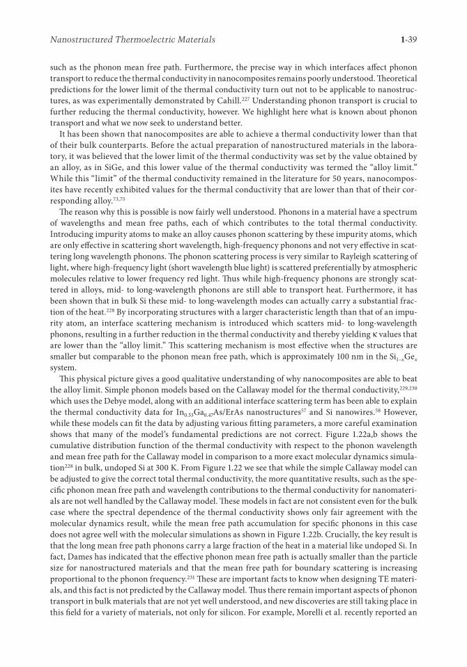
1-39Nanostructured Thermoelectric Materials
such as the phonon mean free path. Furthermore, the precise way in which interfaces a¤ect phonon transport to reduce the thermal conductivity in nanocomposites remains poorly understood. �eoretical predictions for the lower limit of the thermal conductivity turn out not to be applicable to nanostruc-tures, as was experimentally demonstrated by Cahill.227 Understanding phonon transport is crucial to further reducing the thermal conductivity, however. We highlight here what is known about phonon transport and what we now seek to understand better.
It has been shown that nanocomposites are able to achieve a thermal conductivity lower than that of their bulk counterparts. Before the actual preparation of nanostructured materials in the labora-tory, it was believed that the lower limit of the thermal conductivity was set by the value obtained by an alloy, as in SiGe, and this lower value of the thermal conductivity was termed the “alloy limit.” While this “limit” of the thermal conductivity remained in the literature for 50 years, nanocompos-ites have recently exhibited values for the thermal conductivity that are lower than that of their cor-responding alloy.73,75
�e reason why this is possible is now fairly well understood. Phonons in a material have a spectrum of wavelengths and mean free paths, each of which contributes to the total thermal conductivity. Introducing impurity atoms to make an alloy causes phonon scattering by these impurity atoms, which are only e¤ective in scattering short wavelength, high-frequency phonons and not very e¤ective in scat-tering long wavelength phonons. �e phonon scattering process is very similar to Rayleigh scattering of light, where high-frequency light (short wavelength blue light) is scattered preferentially by atmospheric molecules relative to lower frequency red light. �us while high-frequency phonons are strongly scat-tered in alloys, mid- to long-wavelength phonons are still able to transport heat. Furthermore, it has been shown that in bulk Si these mid- to long-wavelength modes can actually carry a substantial frac-tion of the heat.228 By incorporating structures with a larger characteristic length than that of an impu-rity atom, an interface scattering mechanism is introduced which scatters mid- to long-wavelength phonons, resulting in a further reduction in the thermal conductivity and thereby yielding κ values that are lower than the “alloy limit.” �is scattering mechanism is most e¤ective when the structures are smaller but comparable to the phonon mean free path, which is approximately 100 nm in the Si1–xGex system.
�is physical picture gives a good qualitative understanding of why nanocomposites are able to beat the alloy limit. Simple phonon models based on the Callaway model for the thermal conductivity,229,230 which uses the Debye model, along with an additional interface scattering term has been able to explain the thermal conductivity data for In0.53Ga0.47As/ErAs nanostructures57 and Si nanowires.58 However, while these models can �t the data by adjusting various �tting parameters, a more careful examination shows that many of the model’s fundamental predictions are not correct. Figure 1.22a,b shows the cumulative distribution function of the thermal conductivity with respect to the phonon wavelength and mean free path for the Callaway model in comparison to a more exact molecular dynamics simula-tion228 in bulk, undoped Si at 300 K. From Figure 1.22 we see that while the simple Callaway model can be adjusted to give the correct total thermal conductivity, the more quantitative results, such as the spe-ci�c phonon mean free path and wavelength contributions to the thermal conductivity for nanomateri-als are not well handled by the Callaway model. �ese models in fact are not consistent even for the bulk case where the spectral dependence of the thermal conductivity shows only fair agreement with the molecular dynamics result, while the mean free path accumulation for speci�c phonons in this case does not agree well with the molecular simulations as shown in Figure 1.22b. Crucially, the key result is that the long mean free path phonons carry a large fraction of the heat in a material like undoped Si. In fact, Dames has indicated that the e¤ective phonon mean free path is actually smaller than the particle size for nanostructured materials and that the mean free path for boundary scattering is increasing proportional to the phonon frequency.231 �ese are important facts to know when designing TE materi-als, and this fact is not predicted by the Callaway model. �us there remain important aspects of phonon transport in bulk materials that are not yet well understood, and new discoveries are still taking place in this �eld for a variety of materials, not only for silicon. For example, Morelli et al. recently reported an
1-40 Modules, Systems, and Applications in Thermoelectrics
unusually low thermal conductivity in bulk cubic AgSbTe2 due to the extremely anharmonic bonds in this material.232
Nanostructures add another layer of complexity to this problem because they contain many inter-faces with a spacing smaller than the phonon mean free path, and such interfaces introduce a thermal boundary resistance between di¤erent regions of the nanocomposite. While researchers have been able to use a thermal boundary resistance to obtain a low thermal conductivity, there is currently a limited ability to predict the thermal boundary resistance despite many years of research.233,234 A thermal boundary resistance has also been identi�ed as a key mechanism for the low thermal conductivity in superlattices, rather than the periodicity of the superlattices.45,235,238 Such understanding led to the con-cept of using a nanocomposite to enhance the ZT. E¤orts have been made to calculate the thermal boundary resistance using the Boltzmann equation237 and Monte Carlo simulations,238 and Minnich and Chen introduced a modi�ed theory to analytically compute the thermal conductivity of nanocom-posites.239 Similarly, the Peierls instability can also lead to a low thermal conductivity and to ZT enhancement.28
0
10
20
30
40
50
60
70
80
90
100
0102030405060708090
100(a)
(b)
Perc
ent a
ccum
ulat
ion
Perc
ent a
ccum
ulat
ion
10–2 100 102
Mean free path (μm)
CallawayMD simulation
CallawayMD simulation
104
100 101
Wavelength (nm)102
FIGURE 1.22 Cumulative distribution function of the lattice thermal conductivity with respect to (a) phonon wavelength and (b) phonon mean free path predicted by the Callaway model and by molecular dynamics simula-tions in bulk, undoped Si at 300 K. (A¸er A. S. Henry, G. Chen, J. Comput. �eor. Nanosci. 5, 141–152. Copyright 2008, American Scienti�c Publishers.)
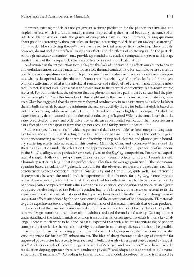
1-41Nanostructured Thermoelectric Materials
However, existing models cannot yet give an accurate prediction for the phonon transmission at a single interface, which is a fundamental parameter in predicting the thermal boundary resistance of an interface. Nanoparticles inside the grains of composites have multiple interfaces, raising questions about phonon scattering by these particles. In the past, scattering models based on Rayleigh scattering57 and acoustic Mie scattering theory240 have been used to treat nanoparticle scattering. �ese models, however, do not include interfacial roughness e¤ects and the e¤ects of scattering inside the particle. Although molecular dynamics241 may provide a potential tool, available computation power at this stage limits the size of the nanoparticles that can be treated in such model calculations.
As discussed in the introduction to this chapter, this lack of understanding a¤ects our ability to design and optimize nanostructured materials to have low thermal conductivity. For example, we are currently unable to answer questions such as which phonon modes are the dominant heat carriers in nanocompos-ites, what is the optimal size distribution of nanostructures, what type of interface leads to the strongest phonon scattering, or what is the interfacial resistance and re¡ectivity of a given nanocomposite inter-face. In fact, it is not even clear what is the lower limit to the thermal conductivity in a nanostructured material. For bulk materials, the criterion that the phonon mean free path must be at least half the pho-non wavelength242,243 sets this lower limit. �is might not be the case in nanostructured materials, how-ever. Chen has suggested that the minimum thermal conductivity in nanostructures is likely to be lower than in bulk materials because the minimum thermal conductivity theory for bulk materials is based on isotropic scattering, while in nanostructures, interfacial scattering is highly anisotropic.244 Cahill has experimentally demonstrated that the thermal conductivity of layered WSe2 is six times lower than the value predicted by theory and only twice that of air, an experimental veri�cation that nanostructures can a¤ect phonon transport in ways that are not accounted for by current theories.227,245
Studies on speci�c materials for which experimental data are available has been one promising strat-egy for advancing our understanding of the key factors for enhancing ZT, such as the control of grain boundary scattering to lower the thermal conductivity, taking both electron and phonon grain bound-ary scattering e¤ects into account. In this context, Minnich, Chen, and coworkers246 have used the Boltzmann equation under the relaxation time approximation to model the TE properties of nanocom-posite Si1–xGex alloys, with particular emphasis given to the Si80Ge20 composition. For typical experi-mental samples, both n- and p-type nanocomposites show dopant precipitation at grain boundaries with a boundary scattering length that is signi�cantly smaller than the average grain size.231 �e Boltzmann-equation-based calculations246 generally account for the observed temperature-dependent electrical conductivity, Seebeck coe´cient, thermal conductivity and ZT of Si1–xGex quite well. Two interesting discrepancies between the model and the experimental data obtained for a Si80Ge20 nanocomposite material are especially informative. First, the calculated hole e¤ective mass has to be increased for the nanocomposites compared to bulk values with the same chemical composition and the calculated grain boundary barrier height of the Poisson equation has to be increased by a factor of several to �t the experimental data. Model calculations of this type have been found to be e¤ective in clarifying the most important e¤ects introduced by the nanostructuring of the constituents of nanocomposite TE materials to guide experiments toward optimizing the performance of the actual materials that we can produce.
It is clear that there are many unanswered questions in phonon transport theory that critically a¤ect how we design nanostructured materials to exhibit a reduced thermal conductivity. Gaining a better understanding of the fundamentals of phonon transport in nanostructured materials is thus a key chal-lenge. �ere is much work to be done, but it is expected that with a better understanding of phonon transport, further lattice thermal conductivity reductions in nanocomposite systems should be possible.
In addition to further reducing phonon thermal conductivity, improving electron transport is also very important for further ZT enhancements. �e idea of sharp features in density of states44,84 for improved power factor has recently been realized in bulk materials via resonant states caused by impuri-ties.82 Another example of such a strategy is the work of Zebarjadi and coworkers,247 who have taken the modulation doping approach from semiconductor physics248 and adapted this approach to bulk nano-structured TE materials.247 According to this approach, the modulation-doped sample is prepared by
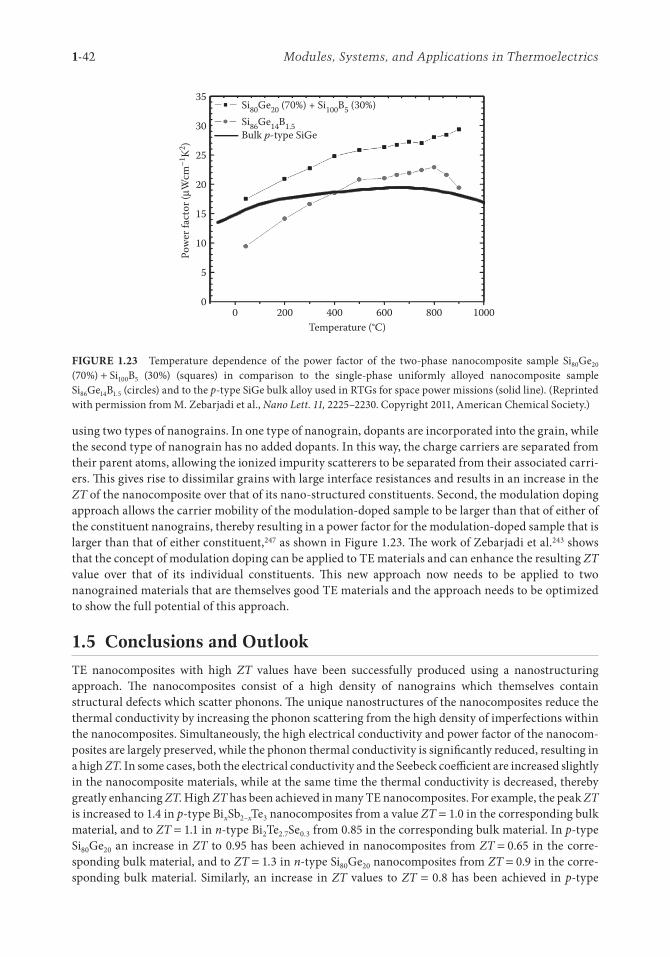
1-42 Modules, Systems, and Applications in Thermoelectrics
using two types of nanograins. In one type of nanograin, dopants are incorporated into the grain, while the second type of nanograin has no added dopants. In this way, the charge carriers are separated from their parent atoms, allowing the ionized impurity scatterers to be separated from their associated carri-ers. �is gives rise to dissimilar grains with large interface resistances and results in an increase in the ZT of the nanocomposite over that of its nano-structured constituents. Second, the modulation doping approach allows the carrier mobility of the modulation-doped sample to be larger than that of either of the constituent nanograins, thereby resulting in a power factor for the modulation-doped sample that is larger than that of either constituent,247 as shown in Figure 1.23. �e work of Zebarjadi et al.243 shows that the concept of modulation doping can be applied to TE materials and can enhance the resulting ZT value over that of its individual constituents. �is new approach now needs to be applied to two nanograined materials that are themselves good TE materials and the approach needs to be optimized to show the full potential of this approach.
1.5 Conclusions and Outlook
TE nanocomposites with high ZT values have been successfully produced using a nanostructuring approach. �e nanocomposites consist of a high density of nanograins which themselves contain structural defects which scatter phonons. �e unique nanostructures of the nanocomposites reduce the thermal conductivity by increasing the phonon scattering from the high density of imperfections within the nanocomposites. Simultaneously, the high electrical conductivity and power factor of the nanocom-posites are largely preserved, while the phonon thermal conductivity is signi�cantly reduced, resulting in a high ZT. In some cases, both the electrical conductivity and the Seebeck coe´cient are increased slightly in the nanocomposite materials, while at the same time the thermal conductivity is decreased, thereby greatly enhancing ZT. High ZT has been achieved in many TE nanocomposites. For example, the peak ZT is increased to 1.4 in p-type BixSb2–xTe3 nanocomposites from a value ZT = 1.0 in the corresponding bulk material, and to ZT = 1.1 in n-type Bi2Te2.7Se0.3 from 0.85 in the corresponding bulk material. In p-type Si80Ge20 an increase in ZT to 0.95 has been achieved in nanocomposites from ZT = 0.65 in the corre-sponding bulk material, and to ZT = 1.3 in n-type Si80Ge20 nanocomposites from ZT = 0.9 in the corre-sponding bulk material. Similarly, an increase in ZT values to ZT = 0.8 has been achieved in p-type
00
5
10
15
20
25
30
35Si80Ge20 (70%) + Si100B5 (30%)Si86Ge14B1.5Bulk p-type SiGe
200 400 600 800 1000Temperature (°C)
Pow
er fa
ctor
(μW
cm–1
K2 )
FIGURE 1.23 Temperature dependence of the power factor of the two-phase nanocomposite sample Si80Ge20 (70%) + Si100B5 (30%) (squares) in comparison to the single-phase uniformly alloyed nanocomposite sample Si86Ge14B1.5 (circles) and to the p-type SiGe bulk alloy used in RTGs for space power missions (solid line). (Reprinted with permission from M. Zebarjadi et al., Nano Lett. 11, 2225–2230. Copyright 2011, American Chemical Society.)
1-43Nanostructured Thermoelectric Materials
nanocomposite half-Heusler alloys from ZT = 0.5 in the corresponding bulk material. All of these nano-composites with enhanced ZT values have signi�cant commercial potential for cooling, industrial waste heat recovery, space power generation, and solar power conversion applications.
Further investigation is needed to achieve even greater enhancement in ZT which is believed to be possible by researchers working in this �eld. It is believed that this will come both from improvement in the processing of currently used materials and from development of better materials and the introduc-tion of new concepts. In the present nanocomposites, the grain size is usually between 10 and 1000 nm, which is relatively large in comparison with the phonon mean free path. �is is why it is expected that it is still possible to reduce the thermal conductivity of common nanocomposite materials. It should be possible to prepare nanocomposites with smaller grain sizes by limiting the grain growth during the densi�cation process of the nanostructured material. �e smaller grain size will hopefully reduce the thermal conductivity to 1 W m−1 K−1 or less, thereby further enhancing ZT. In order to decrease the thermal conductivity to 1 W m−1 K−1, phonon transport in the nanocomposites needs to be understood in greater detail.
It is reported above that the power factor can be increased in some nanocomposites. However, the thermal conductivity in these nanocomposites is still high, which gives us hope to further improve ZT if the thermal conductivity can be reduced signi�cantly in such cases. In the coming years, it is important to determine e¤ective strategies to simultaneously improve the power factor and reduce the thermal conductivity.
�ere is hope that a ZT value of 2 can be achieved in these nanocomposites if the thermal conductivity is reduced to below 1 W m−1 K−1 and the power factor is further enhanced. �e TE devices fabricated from these high ZT nanocomposites are expected to �nd widespread use in applications such as refrigeration, air conditioning, and high-power commercial generators. It is expected that in the near future, TE devices could contribute signi�cantly to a renewable energy supply in the global marketplace, ensuring a future source of clean, reliable energy while protecting our planet’s environment.
Acknowledgments
�is work has been funded by DOE DE-FG02-00ER45805 (ZFR), DOE DE-FG02-08ER46516 (MD, GC, and ZFR), and DOE DE-SC0001299/DE-FG02-09ER 46577 (GC, MD, and ZFR).
References
1. H. J. Goldsmid, �ermoelectric Refrigeration, Plenum Press, New York, 1964. 2. D. D. Pollock, �ermocouples: �eory and Properties, CRC Press, Boca Raton, FL, 1991. 3. D. M. Rowe, ed. CRC Handbook of �ermoelectrics, CRC Press, Boca Raton, FL, 1995. 4. T. M. Tritt, ed. Recent Trends in �ermoelectric Materials Research III, Vol. 71, Academic Press,
San Diego, CA, 2001. 5. D. M. Rowe, ed. �ermoelectrics Handbook: Macro to Nano, CRC/Taylor & Francis, Boca Raton, FL,
2006. 6. C. Wood, Rep. Prog. Phys. 1988, 51, 459–539; M. Zebarjadi, K. Esfarjani, M. S. Dresselhaus, Z. F.
Ren, G. Chen, Energy Environ. Sci. 2012, 5, 5147–5162. 7. F. J. DiSalvo, Science 1999, 285, 703–706. 8. B. C. Sales, Science 2002, 295, 1248–1249. 9. S. B. Ri¤at, X. Ma, Appl. �erm. Eng. 2003, 23, 913–935. 10. L. E. Bell, Science 2008, 321, 1457–1461. 11. G. J. Snyder, E. S. Toberer, Nat. Mater. 2008, 7, 105–114. 12. D. Kraemer, B. Poudel, H.-P. Feng, J. C. Caylor, B. Yu, X. Yan, Y. Ma et al., Nat. Mater. 2011, 10,
532–538. 13. A. F. Io¤e, Physics of Semiconductors, Academic Press, New York, 1960.
1-44 Modules, Systems, and Applications in Thermoelectrics
14. C. B. Vining, J. Appl. Phys. 1991, 69, 331–341. 15. J. Yang, T. Caillat, MRS Bulletin 2006, 31, 224–229. 16. D. Y. Chung, T. Hogan, P. Brazis, M. Rocci-Lane, C. Kannewurf, M. Bastea, C. Uher, M. G. Kanatzidis,
Science 2000, 287, 1024–1027. 17. B. Wöl�ng, C. Kloc, J. Teubner, E. Bucher, Phys. Rev. Lett. 2001, 86, 4350–4353. 18. V. L. Kuznetsov, L. A. Kuznetsova, A. E. Kaliazin, D. M. Rowe, J. Appl. Phys. 2000, 87, 7871–7875. 19. J. L. Cohn, G. S. Nolas, V. Fessatidis, T. H. Metcalf, G. A. Slack, Phys. Rev. Lett. 1999, 82, 779–782. 20. X. F. Tang, P. Li, S. K. Deng, Q. J. Zhang, J. Appl. Phys. 2008, 104, 013706. 21. S. K. Deng, X. F. Tang, P. Li, Q. J. Zhang, J. Appl. Phys. 2008, 103, 073503. 22. J. Androulakis, C. H. Lin, H. J. Kong, C. Uher, C. Wu, T. Hogan, B. A. Cook, T. Caillat,
K. M. Paraskevopoulos, M. Kanatzidis, J. Am. Chem. Soc. 2007, 129, 9780–9788. 23. K. F. Hsu, S. Loo, F. Guo, W. Chen, J. S. Dyck, C. Uher, T. Hogan, E. K. Polychroniadis, M. G. Kanatzidis,
Science 2004, 303, 818–821. 24. J. Androulakis, K. F. Hsu, R. Pcionek, H. Kong, C. Uher, J. J. D’Angelo, A. Downey, T. Hogan,
M. G. Kanatzidis, Adv. Mater. 2006, 18, 1170–1173. 25. P. F. P. Poudeu, J. D’Angelo, A. D. Downey, J. L. Short, T. P. Hogan, M. G. Kanatzidis, Angew. Chem.
Int. Ed. 2006, 45, 3835–3839. 26. A. Guéguen, P. F. P. Poudeu, C. P. Li, S. Moses, C. Uher, J. He, V. Dravid, K. M. Paraskevopoulos,
M. G. Kanatzidis, Chem. Mater. 2009, 21, 1683–1694. 27. G. S. Nolas, J. Poon, M. Kanatzidis, MRS Bull. 2006, 31, 199–205. 28. J. S. Rhyee, K. H. Lee, S. M. Lee, E. Cho, S. I. Kim, E. Lee, Y. S. Kwon, J. H. Shim, G. Kotliar, Nature
2009, 459, 965–968. 29. G. S. Nolas, J. Sharp, H. J. Goldsmid, �ermoelectrics: Basic Principles and New Materials
Developments, Springer, New York, 2001. 30. M. G. Kanatzidis, S. D. Mahanti, T. P. Hogan, eds. Chemistry, Physics, and Materials Science of
�ermoelectric Materials: Beyond Bismuth Telluride, Kluwer Academic/Plenum Publishers, New York, 2003.
31. K. Koumoto, I. Terasaki, R. Funahashi, MRS Bull. 2006, 31, 206–210. 32. N. Savvides, H. J. Goldsmid, J. Phys. C: Solid State Phys. 1980, 13, 4657–4670. 33. N. Savvides, H. J. Goldsmid, J. Phys. C: Solid State Phys. 1980, 13, 4671–4678. 34. D. M. Rowe, V. S. Shukla, N. Savvides, Nature 1981, 290, 765–766. 35. C. B. Vining, W. Laskow, J. O. Hanson, R. R. V. der Beck, P. D. Gorsuch, J. Appl. Phys. 1991, 69,
4333–4340. 36. D. M. Rowe, L. W. Fu, S. G. K. Williams, J. Appl. Phys. 1993, 73, 4683–4685. 37. A. A. Joraide, J. Mater. Sci. 1995, 30, 744–748. 38. C. W. Nan, R. Birringer, Phys. Rev. B 1998, 57, 8264–8268. 39. D. B. Hyun, J. S. Hwang, J. D. Shim, J. Mater. Sci. 2001, 36, 1285–1291. 40. D. H. Kim, T. Mitani, J. Alloy Compd. 2005, 399, 14–19. 41. G. Chen, 2001, in Semiconductors and Semimetals, Recent Trends in �ermoelectric Materials
Research III, Vol. 71 (Ed. T. Tritt), Academic Press, San Diego, CA, 2001, pp. 203–259. 42. G. Chen, M. S. Dresselhaus, J.-P. Fleurial, T. Caillat, Int. Mat. Rev. 2003, 48, 45–66. 43. G. Chen, A. Shakouri, ASME J. Heat Transfer 2002, 124, 242–252. 44. L. D. Hicks, M. S. Dresselhaus, Phys. Rev. B 1993, 47, 16631–16634. 45. G. Chen, Phys. Rev. B 1998, 57, 14958–14973. 46. H. Q. Liu, Y. Song, S. N. Zhang, X. B. Zhao, F. P. Wang, J. Phys. Chem. Solids 2009, 70, 600–603. 47. M. S. Dresselhaus, G. Chen, M. Y. Tang, R. G. Yang, H. Lee, D. Z. Wang, Z. F. Ren, J. P. Fleurial,
P. Gogna, Adv. Mater. 2007, 19, 1043–1053. 48. T. Koga, S. B. Cronin, M. S. Dresselhaus, J. L. Liu, K. L. Wang, Appl. Phys. Lett. 2000, 77,
1490–1492.
1-45Nanostructured Thermoelectric Materials
49. X. B. Zhao, S. H. Yang, Y. Q. Cao, J. L. Mi, Q. Zhang, T. J. Zhu, J. Electron. Mater. 2009, 38, 1017–1024.
50. Q. Zhang, J. He, T. J. Zhu, S. N. Zhang, X. B. Zhao, T. M. Tritt, Appl. Phys. Lett. 2008, 93, 102109. 51. R. Venkatasubramanian, E. Siivola, T. Colpitts, B. O’Quinn, Nature 2001, 413, 597–602. 52. Q. Zhang, J. He, X. B. Zhao, S. N. Zhang,T. J. Zhu, H. Yin, T. M. Tritt, J. Phys. D: Appl. Phys. 2008, 41,
185103. 53. Q. Zhang, X. B. Zhao, H. Yin, T. J. Zhu, J. Alloys. Compd. 2008, 464, 9–12. 54. Y. Q. Cao, T. J. Zhu, X. B. Zhao, X. B. Zhang, J. P. Tu, Appl. Phys. A 2008, 92, 321–324. 55. T. C. Harman, P. J. Taylor, M. P. Walsh, B. E. LaForge, Science 2002, 297, 2229–2232. 56. W. J. Xie, X. F. Tang, Y. G. Yan, Q. J. Zhang, T. M. Tritt, Appl. Phys. Lett. 2009, 94, 102111. 57. W. Kim, J. Zide, A. Gossard, D. Klenov, S. Stemmer, A. Shakouri, A. Majumdar, Phys. Rev. Lett. 2006,
96, 045901. 58. A. I. Hochbaum, R. Chen, R. D. Delgado, W. Liang, E. C. Garnett, M. Najarian, A. Majumdar,
P. Yang, Nature 2008, 451, 163–167. 59. A. I. Boukai, Y. Bunimovich, J. Tahir-Kheli, J. K. Yu, W. A. Goddard III, J. R. Heath, Nature 2008,
451, 168–171. 60. D. Li, Y. Wu, P. Kim, L. Shi, P. Yang, A. Majumdar, Appl. Phys. Lett. 2003, 83, 2934. 61. J. Zhou, Q. Jin, J. H. Seol, X. Li, L. Shi, Appl. Phys. Lett. 2005, 87, 133109. 62. T. Yao, Appl. Phys. Lett. 1987, 51, 1798–1800. 63. G. Chen, C. L. Tien, X. Wu, J. S. Smith, J. Heat Transfer, 1994, 116, 325–331. 64. X. Y. Yu, G. Chen, A. Verma, J. S. Smith, Appl. Phys. Lett., 1995, 67, 3554–3556. 65. G. Chen, C. L. Tien, J. �ermophys. Heat Transfer, 1993, 7, 311–318. 66. S. Lee, D. Cahill, R. Venkatasubramanian, Appl. Phys. Lett. 1997, 70, 2957–2959. 67. H. Böttner, G. Chen, R. Venkatasubramanian, MRS Bull. 2006, 31, 211–217. 68. J. P. Heremans, C. M. �rush, D. T. Morelli, Phys. Rev. B 2004, 70, 115334. 69. S. M. Lee, D. G. Cahill, R. Venkatasubramanian, Appl. Phys. Lett. 1997, 70, 2957–2959. 70. B. Yang, W. L. Liu, J. L. Liu, K. L. Wang, G. Chen, Appl. Phys. Lett. 2002, 81, 3588–3590. 71. Y. Zhang, J. Christo¤erson, A. Shakouri, D. Li, A. Majumdar, Y. Wu, R. Fan, P. Yang, IEEE Trans.
Nanotechnol. 2006, 5, 67–74. 72. B. Poudel, Q. Hao, Y. Ma, Y. C. Lan, A. Minnich, B. Yu, X. Yan et al., Science 2008, 320, 634–638. 73. G. Joshi, H. Lee, Y. C. Lan, X. W. Wang, G. H. Zhu, D. Z. Wang, R. W. Gould et al., Nano Lett. 2008,
8, 4670–4674. 74. Y. Ma, Q. Hao, B. Poudel, Y. C. Lan, B. Yu, D. Z. Wang, G. Chen, Z. F. Ren, Nano Lett. 2008, 8,
2580–2584. 75. X. W. Wang, H. Lee, Y. C. Lan, G. H. Zhu, G. Joshi, D. Z. Wang, J. Yang et al., Appl. Phys. Lett. 2008,
93, 193121. 76. G. H. Zhu, H. Lee, Y. C. Lan, X. W. Wang, G. Joshi, D. Z. Wang, J. Yang et al., Phys. Rev. Lett. 2009,
102, 196803. 77. Z. F. Ren, B. Poudel, Y. Ma, Q. Hao, Y. C. Lan, A. Minnich, A. Muto et al., Mater. Res. Soc. Symp.
Proc., 2009, 1166, 1166. 78. S. Bhattacharya, A. L. Pope, R. T. L. IV, T. M. Tritt, V. Ponnambalam, Y. Xia, S. J. Poon, Appl. Phys.
Lett. 2000, 77, 2476–2478. 79. J. P. Heremans, C. M. �rush, D. T. Morelli, J. Appl. Phys. 2005, 98, 063703. 80. J. M. O. Zide, D. Vashaee, Z. X. Bian, G. Zeng, J. E. Bowers, A. Shakouri, A. C. Gossard, Phys. Rev. B
2006, 74, 205335. 81. H. Ohta, S. Kim, Y. Mune, T. Mizoguchi, K. Nomura, S. Ohta, T. Nomura et al., Nat. Mater. 2007, 6,
129–134. 82. J. P. Heremans, V. Jovovic, E. S. Toberer, A. Saramat, K. Kurosaki, A. Charoenphakdee, S. Yamanaka,
G. J. Snyder, Science 2008, 321, 554–557.
1-46 Modules, Systems, and Applications in Thermoelectrics
83. B. Yu, Q. Y. Zhang, H. Wang. X. W. Wang, H. Z. Wang, D. Z. Wang, H. Wang, G. J. Snyder, G. Chen, Z. F. Ren, J. Appl. Phys. 2010, 108, 016104.
84. G. D. Mahan, J. O. Sofo, Proc. Natl. Acad. Sci. USA 1996, 93, 7436–7439. 85. M. Dresselhaus, G. Dresselhaus, X. Sun, Z. Zhang, S. Cronin, T. Koga, Phys. Solid State 1999, 41,
679–682. 86. M. S. Dresselhaus, G. Chen, M. Y. Tang, R. G. Yang, H. Lee, D. Wang, Z. F. Ren, J. P. Fleurial, P. Gogna,
Mater. Res. Soc. Symp. Proc., 2006, 886, 0886. 87. H. Ni, T. Zhu, X. Zhao, Physica B 2005, 364, 50–54. 88. T. J. Zhu, Y. Q. Liu, X. B. Zhao, Mater. Res. Bull. 2008, 43, 2850–2854. 89. W. Z. Wang, B. Poudel, J. Yang, D. Z. Wang, Z. F. Ren, J. Am. Chem. Soc. 2005, 127, 13792–13793. 90. J. L. Mi, X. B. Zhao, T. J. Zhu, J. P. Tu, Mater. Lett. 2008, 62, 2363–2365. 91. Y. Q. Cao, T. J. Zhu, X. B. Zhao, J. Alloys. Compd. 2008, 449, 109–112. 92. W. Z. Wang, B. Poudel, D. Z. Wang, Z. F. Ren, Adv. Mater. 2005, 17, 2110–2114. 93. B. Poudel, W. Z. Wang, D. Z. Wang, J. Y. Huang, Z. F. Ren, J. Nanosci. Nanotechnol. 2006, 6,
1050–1053. 94. W. Z. Wang, X. Yan, B. Poudel, Y. Ma, Q. Hao, J. Yang, G. Chen, Z. F. Ren, J. Nanosci. Nanotechnol.
2008, 8, 452–456. 95. Y. Q. Cao, X. B. Zhao, T. J. Zhu, X. B. Zhang, J. P. Tu, Appl. Phys. Lett. 2008, 92, 143106. 96. L. Bertini, C. Stiewe, M. Toprak, S. Williams, D. Platzek, A. Mrotzek, Y. Zhang et al., J. Appl. Phys.
2003, 93, 438–447. 97. T. Sun, X. B. Zhao, T. J. Zhu, J. P. Tu, Mater. Lett. 2006, 60, 2534–2537. 98. J. Martin, G. S. Nolas, W. Zhang, L. Chen, Appl. Phys. Lett. 2007, 90, 222112. 99. Y. Y. Zheng, T. J. Zhu, X. B. Zhao, J. P. Tu, G. S. Cao, Mater. Lett. 2005, 59, 2886–2888. 100. K. Sridhar, K. Chattopadhyay, J. Alloy Compd. 1998, 264, 293–298. 101. R. Martin-Lopez, A. Dauscher, H. Scherrer, J. Hejtmanek, H. Kenzari, B. Lenoir, Appl. Phys. A:
Mater. Sci. Process. 1999, 68, 597–602. 102. J. Schilz, M. Ri¤el, K. Pixius, H. J. Meyer, Powder Technol. 1999, 105, 149–154. 103. K. Kishimoto, T. Koyanagi, J. Appl. Phys. 2002, 92, 2544–2549. 104. S. S. Kim, S. Yamamoto, T. Aizawa, J. Alloy Compd. 2004, 375, 107–113. 105. J. Yang, X. Fan, R. Chen, W. Zhu, S. Bao, X. Duan, J. Alloy Compd. 2006, 416, 270–273. 106. J. Yang, R. Chen, X. Fan, S. Bao, W. Zhu, J. Alloy Compd. 2006, 407, 330–333. 107. H. Wang, J. F. Li, C. W. Nan, M. Zhou, W. Liu, B. P. Zhang, T. Kita, Appl. Phys. Lett. 2006, 88, 092104. 108. W. S. Liu, B. P. Zhang, J. F. Li, L. D. Zhao, J. Phys. D: Appl. Phys. 2007, 40, 566–572. 109. W. S. Liu, B. P. Zhang, L. D. Zhao, J. F. Li, Chem. Mater. 2008, 20, 7526–7531. 110. M. Zakeri, M. Allahkarami, G. Kavei, A. Khanmohammadian, M. Rahimipour, J. Mater. Process.
Technol. 2009, 209, 96–101. 111. C. Suryanarayana, Prog. Mater. Sci. 2001, 46, 1–184. 112. P. S. Gilman, J. S. Benjamin, Annu. Rev. Mater. Res. 1983, 13, 279–300. 113. R. Davis, C. Koch, Scripta Metall. 1987, 21, 305–310. 114. C. C. Koch, Annu. Rev. Mater. Res. 1989, 19, 121–143. 115. H. Li, X. F. Tang, X. L. Su, Q. J. Zhang, Appl. Phys. Lett. 2008, 92, 202114. 116. T. Kumpeerapun, H. Scherrer, J. Khedari, J. Hirunlabh, S. Weber, A. Dauscher, B. Lenoir, B. Zighmati,
H. M. Jahed, V. Kosalathip, in Proc. of 25th International Conference on �ermoelectrics, Vienna, Austria, 2006, pp. 136–140.
117. J. Peng, J. Yang, T. Zhang, X. Song, Y. Chen, J. Alloy Compd. 2004, 381, 313–316. 118. S. C. Ur, I. H. Kim, P. Nash, J. Mater. Sci. 2007, 42, 2143–2149. 119. C. J. Liu, H. Yamauchi, Phys. Rev. B 1995, 51, 11826–11829. 120. J. L. Harringa, B. A. Cook, Mater. Sci. Eng. B 1999, 60, 137–142. 121. Z. He, C. Stiewe, D. Platzek, G. Karpinski, E. Muller, S. Li, M. Toprak, M. Muhammed, J. Appl. Phys.
2007, 101, 053713.
1-47Nanostructured Thermoelectric Materials
122. J. M. Schultz, J. P. McHugh, W. A. Tiller, J. Appl. Phys. 1962, 33, 2443–2450. 123. R. Lefever, G. McVay, R. Baughman, Mater. Res. Bull. 1974, 9, 863–872. 124. N. Savvides, H. J. Goldsmid, J. Mater. Sci. 1980, 15, 594–600. 125. J. F. Miller, R. C. Himes, J. Electrochem. Soc. 1960, 107, 915–919. 126. D. M. Rowe, R. W. Bunce, J. Phys. D: Appl. Phys. 1969, 2, 1497–1502. 127. J. Yang, Q. Hao, H. Wang, Y. C. Lan, Q. Y. He, D. Z. Wang, J. A. Harriman et al., Phys. Rev. B 2009, 80,
115329. 128. Q. Y. He, Q. Hao, X. W. Wang, J. Yang, Y. C. Lan, X. Yan, B. Yu et al., J. Nanosci. Nanotechnol. 2008,
8, 4003–4006. 129. Q. Y. He, S. J. Hu, X. G. Tang, Y. C. Lan, J. Yang, X. W. Wang, Z. F. Ren, Q. Hao, G. Chen, Appl. Phys.
Lett. 2008, 93, 042108. 130. C. B. Murray, C. R. Kagan, M. G. Bawendi, Annu. Rev. Mater. Sci. 2000, 30, 545–610. 131. Y. C. Lan, B. Poudel, Y. Ma, D. Z. Wang, M. S. Dresselhaus, G. Chen, Z. F. Ren, Nano Lett. 2009, 9,
1419–1422. 132. D. Medlin, G. Snyder, Curr. Opin. Colloid Interface Sci. 2009, 14, 226–235. 133. J. Yang, T. Aizawa, A. Yamamoto, T. Ohta, J. Alloy Compd. 2000, 309, 225–228. 134. J. Yang, T. Aizawa, A. Yamamoto, T. Ohta, Mater. Chem. Phys. 2001, 70, 90–94. 135. N. Miyashita, T. Yano, R. Tsukuda, I. Yashima, J. Ceram. Soc. Jpn. 2003, 111, 386–390. 136. H. J. Im, D. H. Kim, T.Mitani, K. C. Je, Jpn. J. Appl. Phys. 2004, 43, 1094–1099. 137. X. Fan, J. Yang, R. Chen, W. Zhu, S. Bao, Mater. Sci. Eng. A 2006, 438–440, 190–193. 138. X. Zhao, S. Yang, Y. Cao, J. Mi, Q. Zhang, T. Zhu, J. Electron. Mater. 2009, 38, 1017–1024. 139. H. C. Kim, T. S. Oh, D. B. Hyun, J. Phys. Chem. Solids 2000, 61, 743–749. 140. H. Ni, X. Zhao, T. Zhu, X. Ji, J. Tu, J. Alloy Compd. 2005, 397, 317–321. 141. X. Tang, W. Xie, H. Li, W. Zhao, Q. Zhang, M. Niino, Appl. Phys. Lett. 2007, 90, 012102. 142. O. B. Sokolov, S. Y. Skipidarov, N. I. Duvankov, J. Cryst. Growth 2002, 236, 181. 143. M. Carle, P. Pierrat, C. Lahalle-Gravier, S. Scherrer, H. Scherrer, J. Phys. Chem. Solids 1995, 56, 201. 144. R. Yang, G. Chen, Phys. Rev. B 2004, 69, 195316. 145. O. Ben-Yehuda, Y. Gelbstein, Z. Dashevsky, R. Shuker, M. P. Dariel, Proc. of the 25th ICT 2006, 492. 146. L. D. Zhao, B.-P. Zhang, J.-F. Li, H. L. Zhang, W. S. Liu, Solid State Sci. 2008, 10, 651. 147. X. Yan, B. Poudel, Y. Ma, W. S. Liu, G. Joshi, H. Wang, Y. C. Lan, D. Z. Wang, G. Chen, Z. F. Ren,
Nano Lett. 2010, 10, 3373–3378. 148. J. Jiang, L. D. Chen, S. Q. Bai, Q. Yao, Q. Wang, Mater. Sci. Eng. B 2005, 117, 334. 149. S. J. Hong, Y. S. Lee, J. W. Byeon, B. S. Chun, J. Alloys Compd. 2006, 414, 146. 150. J. T. Im, K. T. Hartwig, J. Sharp, Acta Mater. 2004, 52, 49. 151. T. S. Kim, B. S. Chun, Mater. Sci. Forum 2007, 161, 534–536. 152. W. J. Xie, X. F. Tang, G. Chen, Q. Jin, Q. J. Zhang, Proc. of the 26th ICT 2007, 23. 153. Z. F. Ren, J. H. Wang, D. J. Miller, K. C. Goretta, Physica C 1994, 229, 137. 154. I. Yashima, H. Watanave, T. Ogisu, R. Tsukuda, S. Sato, Jpn. J. Appl. Phys. 1998, 37, 2472–2473. 155. J. Seo, K. Park, D. Lee, C. Lee, Mater. Sci. Eng. B 1997, 49, 247–250. 156. G. A. Slack, M. A. Hussain, J. Appl. Phys. 1991, 70, 2694–2718. 157. B. Abeles, Phys. Rev. 1963, 131, 1906–1911. 158. N. K. Abrikosov, V. S. Zemskov, E. K. Iordanishvili, A. V. Petrov, V. V. Rozhdestvenskaya, Sov. Phys.
Semicond. 1968, 2, 1762. 159. J. P. Dismukes, L. Ekstrom, E. F. Steigmeier, I. Kudman, D. S. Beers, J. Appl. Phys. 1964, 35,
2899–2907. 160. C. M. Bhandari, D. M. Rowe, Contemp. Phys. 1980, 21, 219–242. 161. M. Abdellaoui, E. Ga¤et, J. Phys. IV France 1994, 4, C3-291–C3-296. 162. E. Ga¤et, L. Yous�, Mater. Sci. Forum 1992, 88–90, 51–58. 163. H. Bakker, L. M. Di, Mater. Sci. Forum 1994, 88–90, 27–34. 164. D. M. Rowe, J. Phys. D: Appl. Phys. 1974, 7, 1843–1846.
1-48 Modules, Systems, and Applications in Thermoelectrics
165. S. K. Bux, R. G. Blair, P. K. Gogna, H. Lee, G. Chen, M. S. Dresselhaus, R. B. Kaner, J. P. Fleurial, Adv. Funct. Mater. 2009, 19, 2445–2452.
166. B. C. Sales, D. Mandrus, R. K. Williams, Science 1996, 272, 1325–1328. 167. J. L. Mi, X. B. Zhao, T. J. Zhu, J. P. Tu, J. Phys. D: Appl. Phys. 2008, 41, 205403. 168. J. L. Mi, X. B. Zhao, T. J. Zhu, J. Ma, J. Alloys Compd. 2008, 452, 225–229. 169. J. L. Mi, X. B. Zhao, T. J. Zhu, J. P. Tu, Appl. Phys. Lett. 2007, 91, 172116. 170. H. Li, X. Tang, Q. Zhang, J. Electron. Mater. 2009, 38, 1224–1228. 171. X. F. Tang, H. Li, Q. J. Zhang, M. Niino, T. Goto, J. Appl. Phys. 2006, 100, 123702. 172. G. S. Nolas, J. L. Cohn, G. A. Slack, Phys. Rev. B 1998, 58, 164–170. 173. Y. Z. Pei, J. Yang, L. D. Chen, W. Zhang, J. R. Salvador, J. Yang, Appl. Phys. Lett. 2009, 95, 042101. 174. S. Q. Bai, Y. Z. Pei, L. D. Chen, W. Q. Zhang, X. Y. Zhao, J. Yang, Acta Mater. 2009, 57,
3135–3139. 175. Y. Z. Pei, S. Q. Bai, X. Y. Zhao, W. Zhang, L. D. Chen, Solid State Sci. 2008, 10, 1422–1428. 176. X. Y. Zhao, X. Shi, L. D. Chen, W. Q. Zhang, S. Q. Bai, Y. Z. Pei, X. Y. Li, T. Goto, Apply. Phys. Lett.
2006, 89, 092121. 177. X. F. Tang, Q. J. Zhang, L. D. Chen, T. Goto, T. Hirai, J. Appl. Phys. 2005, 97, 093712. 178. C. Uher in Advances in �ermoelectric Materials I, Vol. 69 (Ed.: T. Tritt), Academic Press, New York
2001, pp. 139–253. 179. Z. G. Mei, J. Yang, Y. Z. Pei, W. Zhang, L. D. Chen, J. Yang, Phys. Rev. B 2008, 77, 045202. 180. X. Shi, L. D. Chen, S. Q. Bai, X. Y. Huang, X. Y. Zhao, Q. Yao, U. Uher, J. Appl. Phys. 2007, 102,
103709. 181. X. Y. Zhao, X. Shi, L. D. Chen, W. Q. Zhang, W. B. Zhang, Y. Z. Pei, J. Appl. Phys. 2006, 99, 053711. 182. X. Y. Li, L. D. Chen, J. F. Fan, W. B. Zhang, T. Kawahara, T. Hirai, J. Appl. Phys. 2005, 98, 083702. 183. X. F. Tang, L. D. Chen, J. Wang, Q. J. Zhang, T. Goto, T. Hirai, J. Alloys Compd. 2005, 394,
259–264. 184. T. Caillat, A. Borshchevsky, J. P. Fleurial, J. Appl. Phys. 1996, 80, 4442–4449. 185. B. Chen, J. H. Xu, C. Uher, D. T. Morelli, G. P. Meisner, J. P. Fleurial, T. Caillat, A. Borshchevsky, Phys.
Rev. B 1997, 55, 1476–1480. 186. V. Keppens, D. Mandrus, B. C. Sales, B. C. Chakoumakos, P. Dai, R. Coldea, M. B. Maple,
D. A. Gajewski, E. J. Freeman, S. Bennington, Nature 1998, 395, 876–878. 187. M. Puyet, B. Lenoir, A. Dauscher, M. Dehmas, C. Stiewe, E. Muller, J. Appl. Phys. 2004, 95,
4852–4855. 188. L. D. Chen, T. Kawahara, X. F. Tang, T. Goto, T. Hirai, J. S. Dyck, W. Chen, C. Uher, J. Appl. Phys.
2001, 90, 1864–1868. 189. G. S. Nolas, M. Kaeser, R. T. Littleton IV, T. M. Tritt, Appl. Phys. Lett. 2000, 77, 1855–1857. 190. H. Y. Geng, S. Ochi, J. Q. Guo, Appl. Phys. Lett. 2007, 91, 022106. 191. J. Yang, Y. Chen, J. Peng, X. Song, W. Zhu, J. Su, R. Chen, J. Alloy Compd. 2004, 375, 229–232. 192. J. Yang, Y. Chen, W. Zhu, S. Bao, J. Peng, X. Fan, J. Phys. D: Appl. Phys. 2005, 38, 3966–3969. 193. S. Bao, J. Yang, X. Song, J. Peng, W. Zhu, X. Fan, X. Duan, Mater. Sci. Eng. A 2006, 438–440,
186–189. 194. S. C. Ur, I. H. Kim, Mater. Lett. 2002, 57, 543–551. 195. X. Shi, H. Kong, C. P. Li, C. Uher, J. Yang, J. R. Salvador, H. Wang, L. Chen, W. Zhang, Appl. Phys.
Lett. 2008, 92, 182101. 196. S. C. Ur, J. C. Kwon, I. H. Kim, J. Alloy Compd. 2007, 442, 358–361. 197. H. Li, X. F. Tang, Q. J. Zhang, C. Uher, Appl. Phys. Lett. 2008, 93, 252109. 198. S. Bao, J. Yang, W. Zhu, X. Fan, X. Duan, J. Peng, Mater. Lett. 2006, 60, 2029–2032. 199. S. Bao, J. Yang, J. Peng, W. Zhu, X. Fan, X. Song, J. Alloy Compd. 2006, 421, 105–108. 200. B. C. Sales, D. Mandrus, B. C. Chakoumakos, V. Keppens, J. R. �ompson, Phys. Rev. B 1997, 56,
15081–15089. 201. S. Bao, J. Yang, W. Zhu, X. Fan, X. Duan, J. Alloy Compd. 2009, 476, 802–806.
1-49Nanostructured Thermoelectric Materials
202. X. Song, J. Yang, J. Peng, Y. Chen, W. Zhu, T. Zhang, J. Alloys Compd. 2005, 399, 276–279. 203. S. C. Ur, J. C. Kwon, I. H. Kim, Met. Mater. Int. 2008, 14, 625–630. 204. C. Uher, J. Yang, S. Hu, D. T. Morelli, G. P. Meisner, Phys. Rev. B 1999, 59, 8615. 205. S. J. Poon, Recent Trends in �ermoelectric Materials Research II, Semiconductors and Semimetals,
edited by T. M. Tritt (Academic, New York, 2001), 70, 37. 206. W. Jeischko, Metall. Trans. 1970, 1, 3159. 207. Y. Xia, S. Bhattacharya, V. Ponnambalam, A. L. Pope, S. J. Poon, T. M. Tritt, J. Appl. Phys. 2000, 88,
1952. 208. T. Sekimoto, K. Kurosaki, H. Muta, S. Yamanaka, J. Alloys Compd. 2006, 407, 326. 209. T. Wu, W. Jiang, X. Y. Li, Y. F. Zhou, L. D. Chen, J. Appl. Phys. 2007, 102, 103705. 210. V. Ponnambalam, P. N. Alboni, J. Edwards, T. M. Tritt, S. R. Culp, S. J. Poon, J. Appl. Phys. 2008, 103,
063716. 211. S. R. Culp, J. W. Simonson, S. J. Poon, V. Ponnambalam, J. Edwards, T. M. Tritt, Appl. Phys. Lett.
2008, 93, 022105. 212. J. W. Sharp, S. J. Poon, H. J. Goldsmid, Phys. Status Solidi 2001, 187, 507. 213. T. M. Tritt, S. Bhattacharya, Y. Xia, V. Ponnambalam, S. J. Poon, N. �adhani, ICT’01, 2001, 7. 214. S. Katsuyama, T. Kobayashi, Mater. Sci. Eng., B 2010, 166, 99. 215. W. J. Xie, X. F. Tang, Q. J. Zhang, Chin. Phys. 2007, 16, 3549. 216. X. Yan, G. Joshi, W. S. Liu, Y. C. Lan, H. Wang, S. Lee, J. W. Simonson et al., Nano Lett. 2011, 11,
556–560. 217. W. S. Liu, B.-P. Zhang, J.-P. Li, H.-L. Zhang, L.-D. Zhao, J. Appl. Phys. 2007, 102, 103717. 218. W. Xu, L. Li, R. Huang, M. Zhou, L. Zheng, L. Gong, C. Song, Front. Energy Power Eng. China 2009,
3, 90–93. 219. R. J. Huang, L. F. Li, W. Xu, L. H. Gong, Solid State Commun. 2009, 149, 1633–1636. 220. J. Cui, X. Liu, W. Yang, D. Chen, H. Fu, P. Ying, J. Appl. Phys. 2009, 105, 063703. 221. M. Ito, T. Tada, S. Katsuyama, J. Alloy Compd. 2003, 350, 296–302. 222. M. Ito, T. Tada, S. Hara, J. Alloy Compd. 2006, 408-412, 363–367. 223. K. Cai, E. Mueller, C. Drasar, C. Stiewe, Solid State Commun. 2004, 131, 325–329. 224. K. F. Cai, C. W. Nan, Y. Paderno, D. S. McLachlan, Solid State Commun. 2000, 115, 523–526. 225. J. S. Lee, T. S. Oh, D. B. Hyun, J. Mater. Sci. 2000, 35, 881–887. 226. G. J. Snyder, M. Christensen, E. Nishibori, T. Caillat, B. B. Iversen, Nat. Mater. 2004, 3, 458–463. 227. C. Chiritescu, D. G. Cahill, N. Nguyen, D. Johnson, A. Bodapati, P. Keblinski, P. Zschack, Science
2007, 315, 351–353. 228. A. S. Henry, G. Chen, J. Comput. �eor. Nanosci. 2008, 5, 141–152. 229. J. Callaway, Phys. Rev. 1959, 113, 1046–1051. 230. E. F. Steigmeier, B. Abeles, Phys. Rev. 1964, 136, A1149–A1155. 231. Z. Wang, J. E. Alaniz, W. Jang, J. E. Garay, C. Dames, Nano Lett. 2011, 11, 2206–2213. 232. D. T. Morelli, V. Jovovic, J. P. Heremans, Phys. Rev. Lett. 2008, 101, 035901. 233. P. L. Kapitza, J. Phys. (USSR) 1941, 4, 181. 234. E. Schwartz, R. Pohl, Rev. Mod. Phys. 1989, 61, 605–668. 235. G. Chen, J. Heat Transfer 1997, 119, 220–229. 236. G. Chen, T. Zeng, Microscale �ermophys. Eng. 2001, 5, 71–88. 237. R. Prasher, Int. J. Heat Mass Trans. 2005, 48, 4942–4952. 238. H. Zhong, J. R. Lukes, Phys. Rev. B 2006, 74, 125403-1–125403-10. 239. A. Minnich, G. Chen, Appl. Phys. Lett. 2007, 91, 073105-1–073105-3. 240. A. Khitun, K. L. Wang, G. Chen, Nanotechnology 2000, 11, 327–331. 241. Z. Neil, R. L. Jennifer, Phys. Rev. B 2008, 77, 094302. 242. G. A. Slack in Solid State Physics, Vol. 34 (Eds.: F. Seitz, D. Turnbull, H. Ehrenreich), Academic Press,
New York, 1979, pp. 1–71. 243. D. G. Cahill, S. K. Watson, R. O. Pohl, Phys. Rev. B 1992, 46, 6131–6140.
1-50 Modules, Systems, and Applications in Thermoelectrics
244. G. Chen in Phonon Transport in Low-dimensional Structures, Vol. 71 (Ed.: T. M. Tritt), Academic Press, San Diego, CA, 2001, pp. 203–259.
245. A. J. Minnich, M. S. Dresselhaus, Z. F. Ren, G. Chen, Energy Environ. Sci. 2009, 2, 466–479. 246. A. J. Minnich, H. Lee, X. W. Wang, G. Joshi, M. S. Dresselhaus, Z. F. Ren, G. Chen, D. Vashaee, Phys.
Rev. B 2009, 80, 155327. 247. M. Zebarjadi, G. Joshi, G. H. Zhu, B. Yu, A. Minnich, Y. C. Lan, X. W. Wang, M. Dresselhaus, Z. F.
Ren, G. Chen, Nano Lett. 2011, 11, 2225–2230. 248. R. Dingle, H. L. Störmer, A. C. Gossard, W. Wiegmann Appl. Phys. Lett. 1978, 33, 665–667. 249 Y. Lan, A. J. Minnich, G. Chen, and Z. Ren Adv. Func. Mater. 2010, 20, 357–376. Wiley-VCH Verlag
GmbH & Co. KGaA.
References
1 Chapter 1 - NanostructuredThermoelectric Materials
1. H. J. Goldsmid, �ermoelectric Refrigeration, PlenumPress, New York, 1964.
2. D. D. Pollock, �ermocouples: �eory and Properties, CRCPress, Boca Raton, FL, 1991.
3. D. M. Rowe, ed. CRC Handbook of �ermoelectrics, CRCPress, Boca Raton, FL, 1995.
4. T. M. Tritt, ed. Recent Trends in �ermoelectricMaterials Research III, Vol. 71, Academic Press,San Diego, CA, 2001.
5. D. M. Rowe, ed. �ermoelectrics Handbook: Macro to Nano,CRC/Taylor & Francis, Boca Raton, FL, 2006.
6. C. Wood, Rep. Prog. Phys. 1988, 51, 459–539; M.Zebarjadi, K. Esfarjani, M. S. Dresselhaus, Z. F. Ren, G.Chen, Energy Environ. Sci. 2012, 5, 5147–5162.
7. F. J. DiSalvo, Science 1999, 285, 703–706.
8. B. C. Sales, Science 2002, 295, 1248–1249.
9. S. B. Ri¤at, X. Ma, Appl. �erm. Eng. 2003, 23, 913–935.
10. L. E. Bell, Science 2008, 321, 1457–1461.
11. G. J. Snyder, E. S. Toberer, Nat. Mater. 2008, 7,105–114.
12. D. Kraemer, B. Poudel, H.-P. Feng, J. C. Caylor, B. Yu,X. Yan, Y. Ma et al., Nat. Mater. 2011, 10, 532–538.
13. A. F. Io¤e, Physics of Semiconductors, Academic Press,New York, 1960.
14. C. B. Vining, J. Appl. Phys. 1991, 69, 331–341.
15. J. Yang, T. Caillat, MRS Bulletin 2006, 31, 224–229.
16. D. Y. Chung, T. Hogan, P. Brazis, M. Rocci-Lane, C.Kannewurf, M. Bastea, C. Uher, M. G. Kanatzidis, Science2000, 287, 1024–1027.
17. B. Wöl�ng, C. Kloc, J. Teubner, E. Bucher, Phys. Rev.Lett. 2001, 86, 4350–4353.
18. V. L. Kuznetsov, L. A. Kuznetsova, A. E. Kaliazin, D.M. Rowe, J. Appl. Phys. 2000, 87, 7871–7875.
19. J. L. Cohn, G. S. Nolas, V. Fessatidis, T. H. Metcalf,G. A. Slack, Phys. Rev. Lett. 1999, 82, 779–782.
20. X. F. Tang, P. Li, S. K. Deng, Q. J. Zhang, J. Appl.Phys. 2008, 104, 013706.
21. S. K. Deng, X. F. Tang, P. Li, Q. J. Zhang, J. Appl.Phys. 2008, 103, 073503.
22. J. Androulakis, C. H. Lin, H. J. Kong, C. Uher, C. Wu,T. Hogan, B. A. Cook, T. Caillat, K. M. Paraskevopoulos,M. Kanatzidis, J. Am. Chem. Soc. 2007, 129, 9780–9788.
23. K. F. Hsu, S. Loo, F. Guo, W. Chen, J. S. Dyck, C.Uher, T. Hogan, E. K. Polychroniadis, M. G. Kanatzidis,Science 2004, 303, 818–821.
24. J. Androulakis, K. F. Hsu, R. Pcionek, H. Kong, C.Uher, J. J. D’Angelo, A. Downey, T. Hogan,M. G. Kanatzidis, Adv. Mater. 2006, 18, 1170–1173.
25. P. F. P. Poudeu, J. D’Angelo, A. D. Downey, J. L.Short, T. P. Hogan, M. G. Kanatzidis, Angew. Chem. Int.Ed. 2006, 45, 3835–3839.
26. A. Guéguen, P. F. P. Poudeu, C. P. Li, S. Moses, C.Uher, J. He, V. Dravid, K. M. Paraskevopoulos,M. G. Kanatzidis, Chem. Mater. 2009, 21, 1683–1694.
27. G. S. Nolas, J. Poon, M. Kanatzidis, MRS Bull. 2006,31, 199–205.
28. J. S. Rhyee, K. H. Lee, S. M. Lee, E. Cho, S. I. Kim,E. Lee, Y. S. Kwon, J. H. Shim, G. Kotliar, Nature 2009,459, 965–968.
29. G. S. Nolas, J. Sharp, H. J. Goldsmid, �ermoelectrics:Basic Principles and New Materials Developments, Springer,New York, 2001.
30. M. G. Kanatzidis, S. D. Mahanti, T. P. Hogan, eds.Chemistry, Physics, and Materials Science of �ermoelectricMaterials: Beyond Bismuth Telluride, Kluwer Academic/PlenumPublishers, New York, 2003.
31. K. Koumoto, I. Terasaki, R. Funahashi, MRS Bull. 2006,31, 206–210.
32. N. Savvides, H. J. Goldsmid, J. Phys. C: Solid StatePhys. 1980, 13, 4657–4670.
33. N. Savvides, H. J. Goldsmid, J. Phys. C: Solid StatePhys. 1980, 13, 4671–4678.
34. D. M. Rowe, V. S. Shukla, N. Savvides, Nature 1981,290, 765–766.
35. C. B. Vining, W. Laskow, J. O. Hanson, R. R. V. derBeck, P. D. Gorsuch, J. Appl. Phys. 1991, 69, 4333–4340.
36. D. M. Rowe, L. W. Fu, S. G. K. Williams, J. Appl. Phys.1993, 73, 4683–4685.
37. A. A. Joraide, J. Mater. Sci. 1995, 30, 744–748.
38. C. W. Nan, R. Birringer, Phys. Rev. B 1998, 57,8264–8268.
39. D. B. Hyun, J. S. Hwang, J. D. Shim, J. Mater. Sci.2001, 36, 1285–1291.
40. D. H. Kim, T. Mitani, J. Alloy Compd. 2005, 399, 14–19.
41. G. Chen, 2001, in Semiconductors and Semimetals, RecentTrends in �ermoelectric Materials Research III, Vol. 71(Ed. T. Tritt), Academic Press, San Diego, CA, 2001, pp.203–259.
42. G. Chen, M. S. Dresselhaus, J.-P. Fleurial, T. Caillat,Int. Mat. Rev. 2003, 48, 45–66.
43. G. Chen, A. Shakouri, ASME J. Heat Transfer 2002, 124,242–252.
44. L. D. Hicks, M. S. Dresselhaus, Phys. Rev. B 1993, 47,16631–16634.
45. G. Chen, Phys. Rev. B 1998, 57, 14958–14973.
46. H. Q. Liu, Y. Song, S. N. Zhang, X. B. Zhao, F. P.Wang, J. Phys. Chem. Solids 2009, 70, 600–603.
47. M. S. Dresselhaus, G. Chen, M. Y. Tang, R. G. Yang, H.Lee, D. Z. Wang, Z. F. Ren, J. P. Fleurial, P. Gogna, Adv.
Mater. 2007, 19, 1043–1053.
48. T. Koga, S. B. Cronin, M. S. Dresselhaus, J. L. Liu, K.L. Wang, Appl. Phys. Lett. 2000, 77, 1490–1492.
49. X. B. Zhao, S. H. Yang, Y. Q. Cao, J. L. Mi, Q. Zhang,T. J. Zhu, J. Electron. Mater. 2009, 38, 1017–1024.
50. Q. Zhang, J. He, T. J. Zhu, S. N. Zhang, X. B. Zhao, T.M. Tritt, Appl. Phys. Lett. 2008, 93, 102109.
51. R. Venkatasubramanian, E. Siivola, T. Colpitts, B.O’Quinn, Nature 2001, 413, 597–602.
52. Q. Zhang, J. He, X. B. Zhao, S. N. Zhang,T. J. Zhu, H.Yin, T. M. Tritt, J. Phys. D: Appl. Phys. 2008, 41,185103.
53. Q. Zhang, X. B. Zhao, H. Yin, T. J. Zhu, J. Alloys.Compd. 2008, 464, 9–12.
54. Y. Q. Cao, T. J. Zhu, X. B. Zhao, X. B. Zhang, J. P.Tu, Appl. Phys. A 2008, 92, 321–324.
55. T. C. Harman, P. J. Taylor, M. P. Walsh, B. E. LaForge,Science 2002, 297, 2229–2232.
56. W. J. Xie, X. F. Tang, Y. G. Yan, Q. J. Zhang, T. M.Tritt, Appl. Phys. Lett. 2009, 94, 102111.
57. W. Kim, J. Zide, A. Gossard, D. Klenov, S. Stemmer, A.Shakouri, A. Majumdar, Phys. Rev. Lett. 2006, 96, 045901.
58. A. I. Hochbaum, R. Chen, R. D. Delgado, W. Liang, E. C.Garnett, M. Najarian, A. Majumdar, P. Yang, Nature 2008,451, 163–167.
59. A. I. Boukai, Y. Bunimovich, J. Tahir-Kheli, J. K. Yu,W. A. Goddard III, J. R. Heath, Nature 2008, 451, 168–171.
60. D. Li, Y. Wu, P. Kim, L. Shi, P. Yang, A. Majumdar,Appl. Phys. Lett. 2003, 83, 2934.
61. J. Zhou, Q. Jin, J. H. Seol, X. Li, L. Shi, Appl. Phys.Lett. 2005, 87, 133109.
62. T. Yao, Appl. Phys. Lett. 1987, 51, 1798–1800.
63. G. Chen, C. L. Tien, X. Wu, J. S. Smith, J. HeatTransfer, 1994, 116, 325–331.
64. X. Y. Yu, G. Chen, A. Verma, J. S. Smith, Appl. Phys.Lett., 1995, 67, 3554–3556.
65. G. Chen, C. L. Tien, J. �ermophys. Heat Transfer, 1993,7, 311–318.
66. S. Lee, D. Cahill, R. Venkatasubramanian, Appl. Phys.Lett. 1997, 70, 2957–2959.
67. H. Böttner, G. Chen, R. Venkatasubramanian, MRS Bull.2006, 31, 211–217.
68. J. P. Heremans, C. M. �rush, D. T. Morelli, Phys. Rev.B 2004, 70, 115334.
69. S. M. Lee, D. G. Cahill, R. Venkatasubramanian, Appl.Phys. Lett. 1997, 70, 2957–2959.
70. B. Yang, W. L. Liu, J. L. Liu, K. L. Wang, G. Chen,Appl. Phys. Lett. 2002, 81, 3588–3590.
71. Y. Zhang, J. Christo¤erson, A. Shakouri, D. Li, A.Majumdar, Y. Wu, R. Fan, P. Yang, IEEE Trans. Nanotechnol.2006, 5, 67–74.
72. B. Poudel, Q. Hao, Y. Ma, Y. C. Lan, A. Minnich, B. Yu,X. Yan et al., Science 2008, 320, 634–638.
73. G. Joshi, H. Lee, Y. C. Lan, X. W. Wang, G. H. Zhu, D.Z. Wang, R. W. Gould et al., Nano Lett. 2008, 8,4670–4674.
74. Y. Ma, Q. Hao, B. Poudel, Y. C. Lan, B. Yu, D. Z. Wang,G. Chen, Z. F. Ren, Nano Lett. 2008, 8, 2580–2584.
75. X. W. Wang, H. Lee, Y. C. Lan, G. H. Zhu, G. Joshi, D.Z. Wang, J. Yang et al., Appl. Phys. Lett. 2008, 93,193121.
76. G. H. Zhu, H. Lee, Y. C. Lan, X. W. Wang, G. Joshi, D.Z. Wang, J. Yang et al., Phys. Rev. Lett. 2009, 102,196803.
77. Z. F. Ren, B. Poudel, Y. Ma, Q. Hao, Y. C. Lan, A.Minnich, A. Muto et al., Mater. Res. Soc. Symp. Proc.,2009, 1166, 1166.
78. S. Bhattacharya, A. L. Pope, R. T. L. IV, T. M. Tritt,V. Ponnambalam, Y. Xia, S. J. Poon, Appl. Phys. Lett.
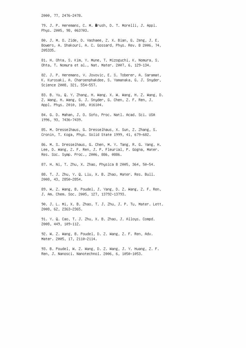
2000, 77, 2476–2478.
79. J. P. Heremans, C. M. �rush, D. T. Morelli, J. Appl.Phys. 2005, 98, 063703.
80. J. M. O. Zide, D. Vashaee, Z. X. Bian, G. Zeng, J. E.Bowers, A. Shakouri, A. C. Gossard, Phys. Rev. B 2006, 74,205335.
81. H. Ohta, S. Kim, Y. Mune, T. Mizoguchi, K. Nomura, S.Ohta, T. Nomura et al., Nat. Mater. 2007, 6, 129–134.
82. J. P. Heremans, V. Jovovic, E. S. Toberer, A. Saramat,K. Kurosaki, A. Charoenphakdee, S. Yamanaka, G. J. Snyder,Science 2008, 321, 554–557.
83. B. Yu, Q. Y. Zhang, H. Wang. X. W. Wang, H. Z. Wang, D.Z. Wang, H. Wang, G. J. Snyder, G. Chen, Z. F. Ren, J.Appl. Phys. 2010, 108, 016104.
84. G. D. Mahan, J. O. Sofo, Proc. Natl. Acad. Sci. USA1996, 93, 7436–7439.
85. M. Dresselhaus, G. Dresselhaus, X. Sun, Z. Zhang, S.Cronin, T. Koga, Phys. Solid State 1999, 41, 679–682.
86. M. S. Dresselhaus, G. Chen, M. Y. Tang, R. G. Yang, H.Lee, D. Wang, Z. F. Ren, J. P. Fleurial, P. Gogna, Mater.Res. Soc. Symp. Proc., 2006, 886, 0886.
87. H. Ni, T. Zhu, X. Zhao, Physica B 2005, 364, 50–54.
88. T. J. Zhu, Y. Q. Liu, X. B. Zhao, Mater. Res. Bull.2008, 43, 2850–2854.
89. W. Z. Wang, B. Poudel, J. Yang, D. Z. Wang, Z. F. Ren,J. Am. Chem. Soc. 2005, 127, 13792–13793.
90. J. L. Mi, X. B. Zhao, T. J. Zhu, J. P. Tu, Mater. Lett.2008, 62, 2363–2365.
91. Y. Q. Cao, T. J. Zhu, X. B. Zhao, J. Alloys. Compd.2008, 449, 109–112.
92. W. Z. Wang, B. Poudel, D. Z. Wang, Z. F. Ren, Adv.Mater. 2005, 17, 2110–2114.
93. B. Poudel, W. Z. Wang, D. Z. Wang, J. Y. Huang, Z. F.Ren, J. Nanosci. Nanotechnol. 2006, 6, 1050–1053.
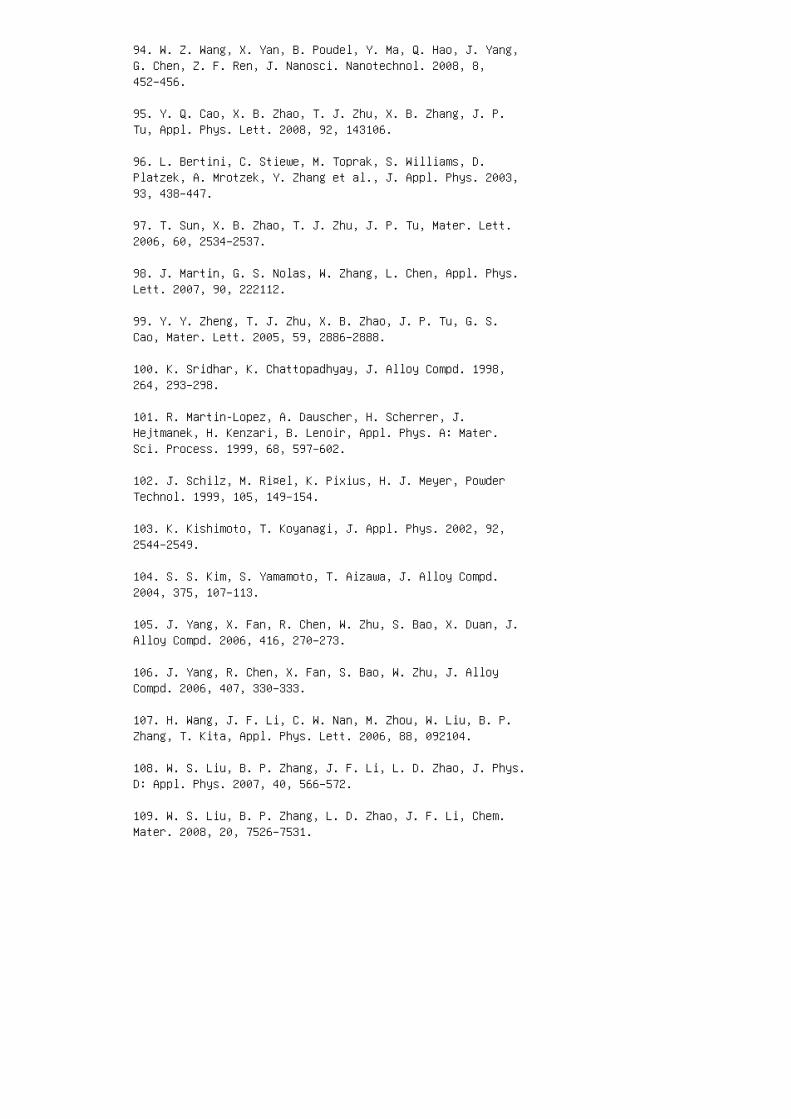
94. W. Z. Wang, X. Yan, B. Poudel, Y. Ma, Q. Hao, J. Yang,G. Chen, Z. F. Ren, J. Nanosci. Nanotechnol. 2008, 8,452–456.
95. Y. Q. Cao, X. B. Zhao, T. J. Zhu, X. B. Zhang, J. P.Tu, Appl. Phys. Lett. 2008, 92, 143106.
96. L. Bertini, C. Stiewe, M. Toprak, S. Williams, D.Platzek, A. Mrotzek, Y. Zhang et al., J. Appl. Phys. 2003,93, 438–447.
97. T. Sun, X. B. Zhao, T. J. Zhu, J. P. Tu, Mater. Lett.2006, 60, 2534–2537.
98. J. Martin, G. S. Nolas, W. Zhang, L. Chen, Appl. Phys.Lett. 2007, 90, 222112.
99. Y. Y. Zheng, T. J. Zhu, X. B. Zhao, J. P. Tu, G. S.Cao, Mater. Lett. 2005, 59, 2886–2888.
100. K. Sridhar, K. Chattopadhyay, J. Alloy Compd. 1998,264, 293–298.
101. R. Martin-Lopez, A. Dauscher, H. Scherrer, J.Hejtmanek, H. Kenzari, B. Lenoir, Appl. Phys. A: Mater.Sci. Process. 1999, 68, 597–602.
102. J. Schilz, M. Ri¤el, K. Pixius, H. J. Meyer, PowderTechnol. 1999, 105, 149–154.
103. K. Kishimoto, T. Koyanagi, J. Appl. Phys. 2002, 92,2544–2549.
104. S. S. Kim, S. Yamamoto, T. Aizawa, J. Alloy Compd.2004, 375, 107–113.
105. J. Yang, X. Fan, R. Chen, W. Zhu, S. Bao, X. Duan, J.Alloy Compd. 2006, 416, 270–273.
106. J. Yang, R. Chen, X. Fan, S. Bao, W. Zhu, J. AlloyCompd. 2006, 407, 330–333.
107. H. Wang, J. F. Li, C. W. Nan, M. Zhou, W. Liu, B. P.Zhang, T. Kita, Appl. Phys. Lett. 2006, 88, 092104.
108. W. S. Liu, B. P. Zhang, J. F. Li, L. D. Zhao, J. Phys.D: Appl. Phys. 2007, 40, 566–572.
109. W. S. Liu, B. P. Zhang, L. D. Zhao, J. F. Li, Chem.Mater. 2008, 20, 7526–7531.
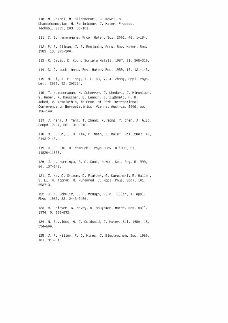
110. M. Zakeri, M. Allahkarami, G. Kavei, A.Khanmohammadian, M. Rahimipour, J. Mater. Process.Technol. 2009, 209, 96–101.
111. C. Suryanarayana, Prog. Mater. Sci. 2001, 46, 1–184.
112. P. S. Gilman, J. S. Benjamin, Annu. Rev. Mater. Res.1983, 13, 279–300.
113. R. Davis, C. Koch, Scripta Metall. 1987, 21, 305–310.
114. C. C. Koch, Annu. Rev. Mater. Res. 1989, 19, 121–143.
115. H. Li, X. F. Tang, X. L. Su, Q. J. Zhang, Appl. Phys.Lett. 2008, 92, 202114.
116. T. Kumpeerapun, H. Scherrer, J. Khedari, J. Hirunlabh,S. Weber, A. Dauscher, B. Lenoir, B. Zighmati, H. M.Jahed, V. Kosalathip, in Proc. of 25th InternationalConference on �ermoelectrics, Vienna, Austria, 2006, pp.136–140.
117. J. Peng, J. Yang, T. Zhang, X. Song, Y. Chen, J. AlloyCompd. 2004, 381, 313–316.
118. S. C. Ur, I. H. Kim, P. Nash, J. Mater. Sci. 2007, 42,2143–2149.
119. C. J. Liu, H. Yamauchi, Phys. Rev. B 1995, 51,11826–11829.
120. J. L. Harringa, B. A. Cook, Mater. Sci. Eng. B 1999,60, 137–142.
121. Z. He, C. Stiewe, D. Platzek, G. Karpinski, E. Muller,S. Li, M. Toprak, M. Muhammed, J. Appl. Phys. 2007, 101,053713.
122. J. M. Schultz, J. P. McHugh, W. A. Tiller, J. Appl.Phys. 1962, 33, 2443–2450.
123. R. Lefever, G. McVay, R. Baughman, Mater. Res. Bull.1974, 9, 863–872.
124. N. Savvides, H. J. Goldsmid, J. Mater. Sci. 1980, 15,594–600.
125. J. F. Miller, R. C. Himes, J. Electrochem. Soc. 1960,107, 915–919.
126. D. M. Rowe, R. W. Bunce, J. Phys. D: Appl. Phys. 1969,2, 1497–1502.
127. J. Yang, Q. Hao, H. Wang, Y. C. Lan, Q. Y. He, D. Z.Wang, J. A. Harriman et al., Phys. Rev. B 2009, 80,115329.
128. Q. Y. He, Q. Hao, X. W. Wang, J. Yang, Y. C. Lan, X.Yan, B. Yu et al., J. Nanosci. Nanotechnol. 2008, 8,4003–4006.
129. Q. Y. He, S. J. Hu, X. G. Tang, Y. C. Lan, J. Yang, X.W. Wang, Z. F. Ren, Q. Hao, G. Chen, Appl. Phys. Lett.2008, 93, 042108.
130. C. B. Murray, C. R. Kagan, M. G. Bawendi, Annu. Rev.Mater. Sci. 2000, 30, 545–610.
131. Y. C. Lan, B. Poudel, Y. Ma, D. Z. Wang, M. S.Dresselhaus, G. Chen, Z. F. Ren, Nano Lett. 2009, 9,1419–1422.
132. D. Medlin, G. Snyder, Curr. Opin. Colloid InterfaceSci. 2009, 14, 226–235.
133. J. Yang, T. Aizawa, A. Yamamoto, T. Ohta, J. AlloyCompd. 2000, 309, 225–228.
134. J. Yang, T. Aizawa, A. Yamamoto, T. Ohta, Mater. Chem.Phys. 2001, 70, 90–94.
135. N. Miyashita, T. Yano, R. Tsukuda, I. Yashima, J.Ceram. Soc. Jpn. 2003, 111, 386–390.
136. H. J. Im, D. H. Kim, T.Mitani, K. C. Je, Jpn. J. Appl.Phys. 2004, 43, 1094–1099.
137. X. Fan, J. Yang, R. Chen, W. Zhu, S. Bao, Mater. Sci.Eng. A 2006, 438–440, 190–193.
138. X. Zhao, S. Yang, Y. Cao, J. Mi, Q. Zhang, T. Zhu, J.Electron. Mater. 2009, 38, 1017–1024.
139. H. C. Kim, T. S. Oh, D. B. Hyun, J. Phys. Chem. Solids2000, 61, 743–749.
140. H. Ni, X. Zhao, T. Zhu, X. Ji, J. Tu, J. Alloy Compd.2005, 397, 317–321.
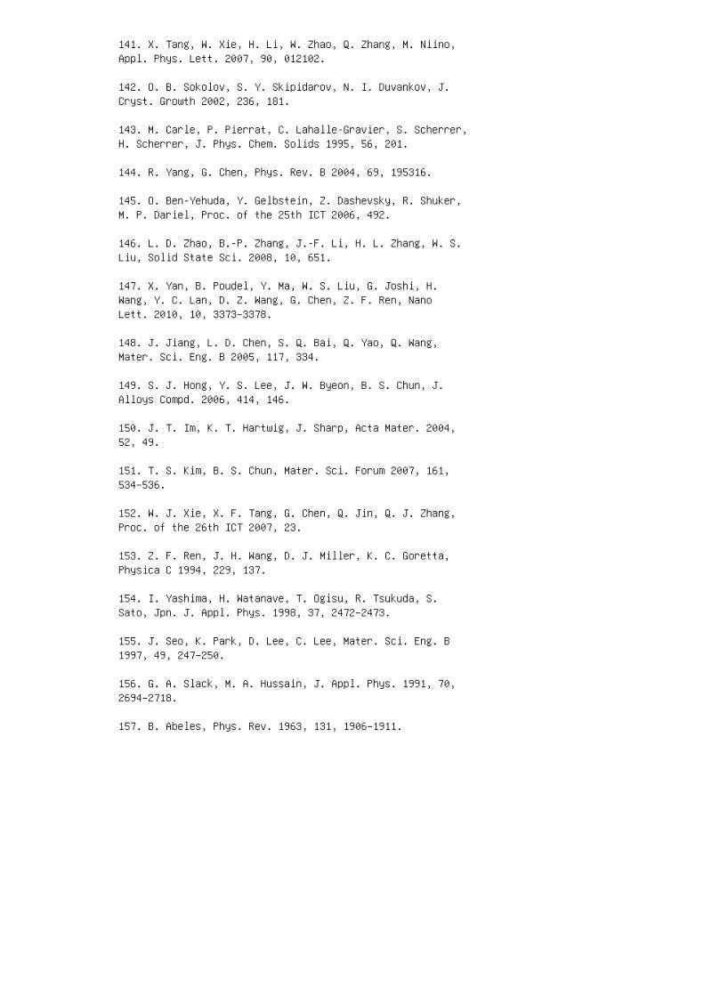
141. X. Tang, W. Xie, H. Li, W. Zhao, Q. Zhang, M. Niino,Appl. Phys. Lett. 2007, 90, 012102.
142. O. B. Sokolov, S. Y. Skipidarov, N. I. Duvankov, J.Cryst. Growth 2002, 236, 181.
143. M. Carle, P. Pierrat, C. Lahalle-Gravier, S. Scherrer,H. Scherrer, J. Phys. Chem. Solids 1995, 56, 201.
144. R. Yang, G. Chen, Phys. Rev. B 2004, 69, 195316.
145. O. Ben-Yehuda, Y. Gelbstein, Z. Dashevsky, R. Shuker,M. P. Dariel, Proc. of the 25th ICT 2006, 492.
146. L. D. Zhao, B.-P. Zhang, J.-F. Li, H. L. Zhang, W. S.Liu, Solid State Sci. 2008, 10, 651.
147. X. Yan, B. Poudel, Y. Ma, W. S. Liu, G. Joshi, H.Wang, Y. C. Lan, D. Z. Wang, G. Chen, Z. F. Ren, NanoLett. 2010, 10, 3373–3378.
148. J. Jiang, L. D. Chen, S. Q. Bai, Q. Yao, Q. Wang,Mater. Sci. Eng. B 2005, 117, 334.
149. S. J. Hong, Y. S. Lee, J. W. Byeon, B. S. Chun, J.Alloys Compd. 2006, 414, 146.
150. J. T. Im, K. T. Hartwig, J. Sharp, Acta Mater. 2004,52, 49.
151. T. S. Kim, B. S. Chun, Mater. Sci. Forum 2007, 161,534–536.
152. W. J. Xie, X. F. Tang, G. Chen, Q. Jin, Q. J. Zhang,Proc. of the 26th ICT 2007, 23.
153. Z. F. Ren, J. H. Wang, D. J. Miller, K. C. Goretta,Physica C 1994, 229, 137.
154. I. Yashima, H. Watanave, T. Ogisu, R. Tsukuda, S.Sato, Jpn. J. Appl. Phys. 1998, 37, 2472–2473.
155. J. Seo, K. Park, D. Lee, C. Lee, Mater. Sci. Eng. B1997, 49, 247–250.
156. G. A. Slack, M. A. Hussain, J. Appl. Phys. 1991, 70,2694–2718.
157. B. Abeles, Phys. Rev. 1963, 131, 1906–1911.
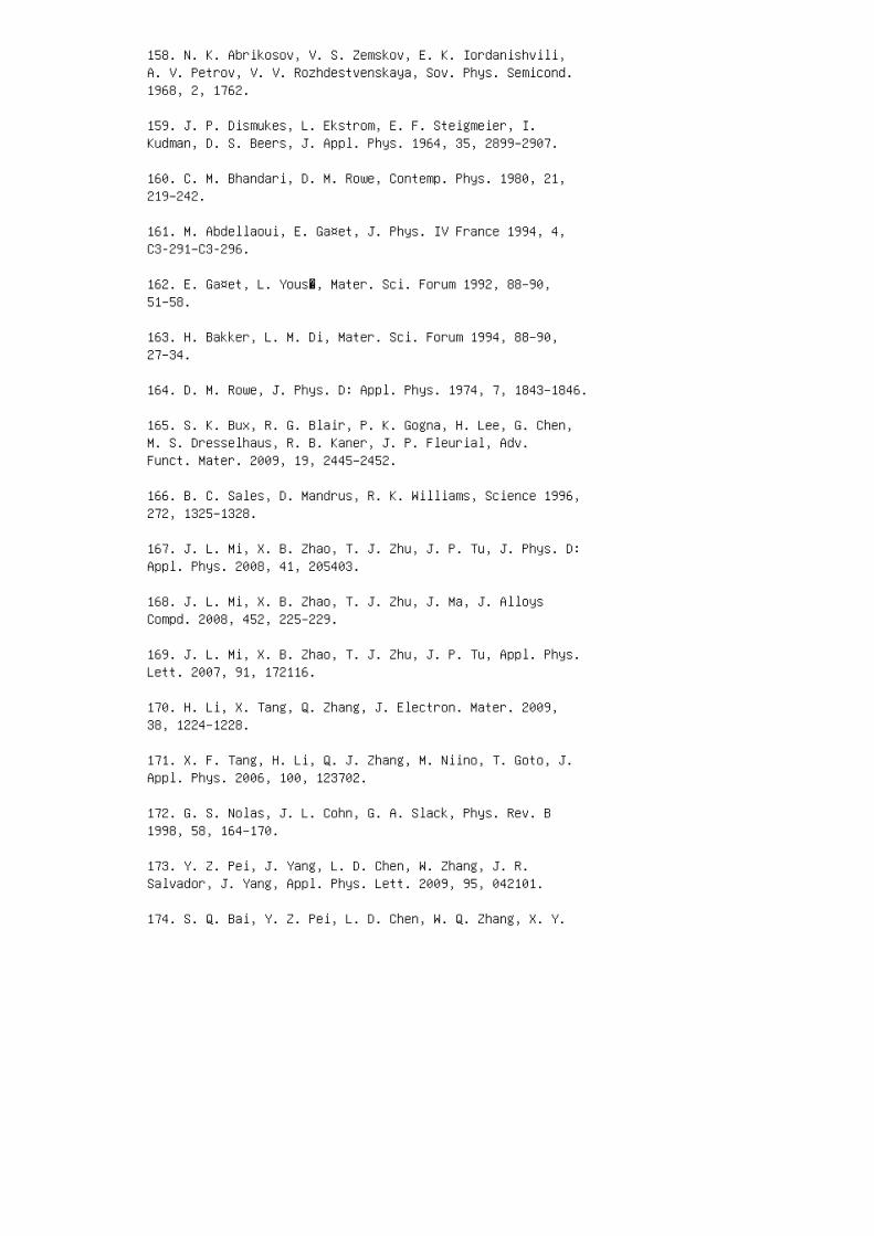
158. N. K. Abrikosov, V. S. Zemskov, E. K. Iordanishvili,A. V. Petrov, V. V. Rozhdestvenskaya, Sov. Phys. Semicond.1968, 2, 1762.
159. J. P. Dismukes, L. Ekstrom, E. F. Steigmeier, I.Kudman, D. S. Beers, J. Appl. Phys. 1964, 35, 2899–2907.
160. C. M. Bhandari, D. M. Rowe, Contemp. Phys. 1980, 21,219–242.
161. M. Abdellaoui, E. Ga¤et, J. Phys. IV France 1994, 4,C3-291–C3-296.
162. E. Ga¤et, L. Yous�, Mater. Sci. Forum 1992, 88–90,51–58.
163. H. Bakker, L. M. Di, Mater. Sci. Forum 1994, 88–90,27–34.
164. D. M. Rowe, J. Phys. D: Appl. Phys. 1974, 7, 1843–1846.
165. S. K. Bux, R. G. Blair, P. K. Gogna, H. Lee, G. Chen,M. S. Dresselhaus, R. B. Kaner, J. P. Fleurial, Adv.Funct. Mater. 2009, 19, 2445–2452.
166. B. C. Sales, D. Mandrus, R. K. Williams, Science 1996,272, 1325–1328.
167. J. L. Mi, X. B. Zhao, T. J. Zhu, J. P. Tu, J. Phys. D:Appl. Phys. 2008, 41, 205403.
168. J. L. Mi, X. B. Zhao, T. J. Zhu, J. Ma, J. AlloysCompd. 2008, 452, 225–229.
169. J. L. Mi, X. B. Zhao, T. J. Zhu, J. P. Tu, Appl. Phys.Lett. 2007, 91, 172116.
170. H. Li, X. Tang, Q. Zhang, J. Electron. Mater. 2009,38, 1224–1228.
171. X. F. Tang, H. Li, Q. J. Zhang, M. Niino, T. Goto, J.Appl. Phys. 2006, 100, 123702.
172. G. S. Nolas, J. L. Cohn, G. A. Slack, Phys. Rev. B1998, 58, 164–170.
173. Y. Z. Pei, J. Yang, L. D. Chen, W. Zhang, J. R.Salvador, J. Yang, Appl. Phys. Lett. 2009, 95, 042101.
174. S. Q. Bai, Y. Z. Pei, L. D. Chen, W. Q. Zhang, X. Y.
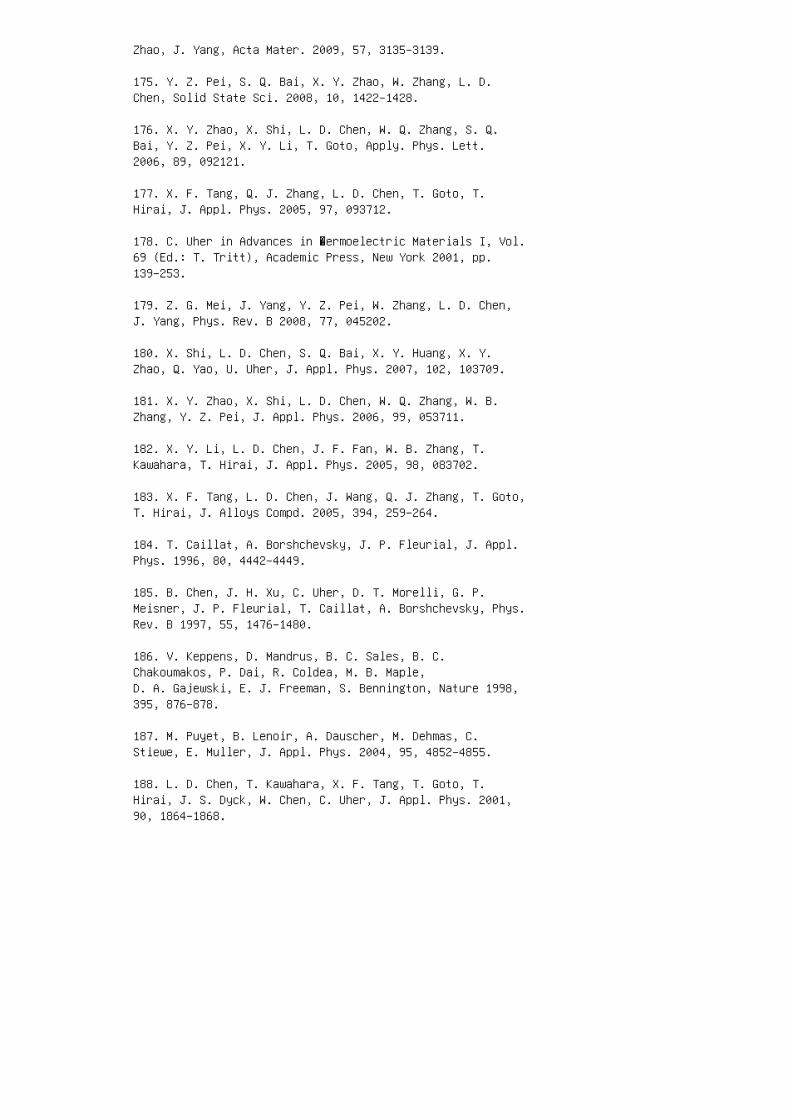
Zhao, J. Yang, Acta Mater. 2009, 57, 3135–3139.
175. Y. Z. Pei, S. Q. Bai, X. Y. Zhao, W. Zhang, L. D.Chen, Solid State Sci. 2008, 10, 1422–1428.
176. X. Y. Zhao, X. Shi, L. D. Chen, W. Q. Zhang, S. Q.Bai, Y. Z. Pei, X. Y. Li, T. Goto, Apply. Phys. Lett.2006, 89, 092121.
177. X. F. Tang, Q. J. Zhang, L. D. Chen, T. Goto, T.Hirai, J. Appl. Phys. 2005, 97, 093712.
178. C. Uher in Advances in �ermoelectric Materials I, Vol.69 (Ed.: T. Tritt), Academic Press, New York 2001, pp.139–253.
179. Z. G. Mei, J. Yang, Y. Z. Pei, W. Zhang, L. D. Chen,J. Yang, Phys. Rev. B 2008, 77, 045202.
180. X. Shi, L. D. Chen, S. Q. Bai, X. Y. Huang, X. Y.Zhao, Q. Yao, U. Uher, J. Appl. Phys. 2007, 102, 103709.
181. X. Y. Zhao, X. Shi, L. D. Chen, W. Q. Zhang, W. B.Zhang, Y. Z. Pei, J. Appl. Phys. 2006, 99, 053711.
182. X. Y. Li, L. D. Chen, J. F. Fan, W. B. Zhang, T.Kawahara, T. Hirai, J. Appl. Phys. 2005, 98, 083702.
183. X. F. Tang, L. D. Chen, J. Wang, Q. J. Zhang, T. Goto,T. Hirai, J. Alloys Compd. 2005, 394, 259–264.
184. T. Caillat, A. Borshchevsky, J. P. Fleurial, J. Appl.Phys. 1996, 80, 4442–4449.
185. B. Chen, J. H. Xu, C. Uher, D. T. Morelli, G. P.Meisner, J. P. Fleurial, T. Caillat, A. Borshchevsky, Phys.Rev. B 1997, 55, 1476–1480.
186. V. Keppens, D. Mandrus, B. C. Sales, B. C.Chakoumakos, P. Dai, R. Coldea, M. B. Maple,D. A. Gajewski, E. J. Freeman, S. Bennington, Nature 1998,395, 876–878.
187. M. Puyet, B. Lenoir, A. Dauscher, M. Dehmas, C.Stiewe, E. Muller, J. Appl. Phys. 2004, 95, 4852–4855.
188. L. D. Chen, T. Kawahara, X. F. Tang, T. Goto, T.Hirai, J. S. Dyck, W. Chen, C. Uher, J. Appl. Phys. 2001,90, 1864–1868.
189. G. S. Nolas, M. Kaeser, R. T. Littleton IV, T. M.Tritt, Appl. Phys. Lett. 2000, 77, 1855–1857.
190. H. Y. Geng, S. Ochi, J. Q. Guo, Appl. Phys. Lett.2007, 91, 022106.
191. J. Yang, Y. Chen, J. Peng, X. Song, W. Zhu, J. Su, R.Chen, J. Alloy Compd. 2004, 375, 229–232.
192. J. Yang, Y. Chen, W. Zhu, S. Bao, J. Peng, X. Fan, J.Phys. D: Appl. Phys. 2005, 38, 3966–3969.
193. S. Bao, J. Yang, X. Song, J. Peng, W. Zhu, X. Fan, X.Duan, Mater. Sci. Eng. A 2006, 438–440, 186–189.
194. S. C. Ur, I. H. Kim, Mater. Lett. 2002, 57, 543–551.
195. X. Shi, H. Kong, C. P. Li, C. Uher, J. Yang, J. R.Salvador, H. Wang, L. Chen, W. Zhang, Appl. Phys. Lett.2008, 92, 182101.
196. S. C. Ur, J. C. Kwon, I. H. Kim, J. Alloy Compd. 2007,442, 358–361.
197. H. Li, X. F. Tang, Q. J. Zhang, C. Uher, Appl. Phys.Lett. 2008, 93, 252109.
198. S. Bao, J. Yang, W. Zhu, X. Fan, X. Duan, J. Peng,Mater. Lett. 2006, 60, 2029–2032.
199. S. Bao, J. Yang, J. Peng, W. Zhu, X. Fan, X. Song, J.Alloy Compd. 2006, 421, 105–108.
200. B. C. Sales, D. Mandrus, B. C. Chakoumakos, V.Keppens, J. R. �ompson, Phys. Rev. B 1997, 56,15081–15089.
201. S. Bao, J. Yang, W. Zhu, X. Fan, X. Duan, J. AlloyCompd. 2009, 476, 802–806.
202. X. Song, J. Yang, J. Peng, Y. Chen, W. Zhu, T. Zhang,J. Alloys Compd. 2005, 399, 276–279.
203. S. C. Ur, J. C. Kwon, I. H. Kim, Met. Mater. Int.2008, 14, 625–630.
204. C. Uher, J. Yang, S. Hu, D. T. Morelli, G. P. Meisner,Phys. Rev. B 1999, 59, 8615.
205. S. J. Poon, Recent Trends in �ermoelectric Materials
Research II, Semiconductors and Semimetals, edited by T.M. Tritt (Academic, New York, 2001), 70, 37.
206. W. Jeischko, Metall. Trans. 1970, 1, 3159.
207. Y. Xia, S. Bhattacharya, V. Ponnambalam, A. L. Pope,S. J. Poon, T. M. Tritt, J. Appl. Phys. 2000, 88, 1952.
208. T. Sekimoto, K. Kurosaki, H. Muta, S. Yamanaka, J.Alloys Compd. 2006, 407, 326.
209. T. Wu, W. Jiang, X. Y. Li, Y. F. Zhou, L. D. Chen, J.Appl. Phys. 2007, 102, 103705.
210. V. Ponnambalam, P. N. Alboni, J. Edwards, T. M. Tritt,S. R. Culp, S. J. Poon, J. Appl. Phys. 2008, 103, 063716.
211. S. R. Culp, J. W. Simonson, S. J. Poon, V.Ponnambalam, J. Edwards, T. M. Tritt, Appl. Phys. Lett.2008, 93, 022105.
212. J. W. Sharp, S. J. Poon, H. J. Goldsmid, Phys. StatusSolidi 2001, 187, 507.
213. T. M. Tritt, S. Bhattacharya, Y. Xia, V. Ponnambalam,S. J. Poon, N. �adhani, ICT’01, 2001, 7.
214. S. Katsuyama, T. Kobayashi, Mater. Sci. Eng., B 2010,166, 99.
215. W. J. Xie, X. F. Tang, Q. J. Zhang, Chin. Phys. 2007,16, 3549.
216. X. Yan, G. Joshi, W. S. Liu, Y. C. Lan, H. Wang, S.Lee, J. W. Simonson et al., Nano Lett. 2011, 11, 556–560.
217. W. S. Liu, B.-P. Zhang, J.-P. Li, H.-L. Zhang, L.-D.Zhao, J. Appl. Phys. 2007, 102, 103717.
218. W. Xu, L. Li, R. Huang, M. Zhou, L. Zheng, L. Gong, C.Song, Front. Energy Power Eng. China 2009, 3, 90–93.
219. R. J. Huang, L. F. Li, W. Xu, L. H. Gong, Solid StateCommun. 2009, 149, 1633–1636.
220. J. Cui, X. Liu, W. Yang, D. Chen, H. Fu, P. Ying, J.Appl. Phys. 2009, 105, 063703.
221. M. Ito, T. Tada, S. Katsuyama, J. Alloy Compd. 2003,350, 296–302.
222. M. Ito, T. Tada, S. Hara, J. Alloy Compd. 2006,408-412, 363–367.
223. K. Cai, E. Mueller, C. Drasar, C. Stiewe, Solid StateCommun. 2004, 131, 325–329.
224. K. F. Cai, C. W. Nan, Y. Paderno, D. S. McLachlan,Solid State Commun. 2000, 115, 523–526.
225. J. S. Lee, T. S. Oh, D. B. Hyun, J. Mater. Sci. 2000,35, 881–887.
226. G. J. Snyder, M. Christensen, E. Nishibori, T.Caillat, B. B. Iversen, Nat. Mater. 2004, 3, 458–463.
227. C. Chiritescu, D. G. Cahill, N. Nguyen, D. Johnson, A.Bodapati, P. Keblinski, P. Zschack, Science 2007, 315,351–353.
228. A. S. Henry, G. Chen, J. Comput. �eor. Nanosci. 2008,5, 141–152.
229. J. Callaway, Phys. Rev. 1959, 113, 1046–1051.
230. E. F. Steigmeier, B. Abeles, Phys. Rev. 1964, 136,A1149–A1155.
231. Z. Wang, J. E. Alaniz, W. Jang, J. E. Garay, C. Dames,Nano Lett. 2011, 11, 2206–2213.
232. D. T. Morelli, V. Jovovic, J. P. Heremans, Phys. Rev.Lett. 2008, 101, 035901.
233. P. L. Kapitza, J. Phys. (USSR) 1941, 4, 181.
234. E. Schwartz, R. Pohl, Rev. Mod. Phys. 1989, 61,605–668.
235. G. Chen, J. Heat Transfer 1997, 119, 220–229.
236. G. Chen, T. Zeng, Microscale �ermophys. Eng. 2001, 5,71–88.
237. R. Prasher, Int. J. Heat Mass Trans. 2005, 48,4942–4952.
238. H. Zhong, J. R. Lukes, Phys. Rev. B 2006, 74,125403-1–125403-10.
239. A. Minnich, G. Chen, Appl. Phys. Lett. 2007, 91,073105-1–073105-3.
240. A. Khitun, K. L. Wang, G. Chen, Nanotechnology 2000,11, 327–331.
241. Z. Neil, R. L. Jennifer, Phys. Rev. B 2008, 77, 094302.
242. G. A. Slack in Solid State Physics, Vol. 34 (Eds.: F.Seitz, D. Turnbull, H. Ehrenreich), Academic Press, NewYork, 1979, pp. 1–71.
243. D. G. Cahill, S. K. Watson, R. O. Pohl, Phys. Rev. B1992, 46, 6131–6140.
244. G. Chen in Phonon Transport in Low-dimensionalStructures, Vol. 71 (Ed.: T. M. Tritt), Academic Press,San Diego, CA, 2001, pp. 203–259.
245. A. J. Minnich, M. S. Dresselhaus, Z. F. Ren, G. Chen,Energy Environ. Sci. 2009, 2, 466–479.
246. A. J. Minnich, H. Lee, X. W. Wang, G. Joshi, M. S.Dresselhaus, Z. F. Ren, G. Chen, D. Vashaee, Phys. Rev. B2009, 80, 155327.
247. M. Zebarjadi, G. Joshi, G. H. Zhu, B. Yu, A. Minnich,Y. C. Lan, X. W. Wang, M. Dresselhaus, Z. F. Ren, G. Chen,Nano Lett. 2011, 11, 2225–2230.
248. R. Dingle, H. L. Störmer, A. C. Gossard, W. WiegmannAppl. Phys. Lett. 1978, 33, 665–667.
249 Y. Lan, A. J. Minnich, G. Chen, and Z. Ren Adv. Func.Mater. 2010, 20, 357–376. Wiley-VCH Verlag GmbH & Co.KGaA.
2 Chapter 2 - Design and Realizationof Nanostructured Inorganic Intergrowths
1. R. Venkatasubramanian, E. Siivola, T. Colpitts, and B.O’Quinn, �in-�lm thermoelectric devices with highroom-temperature �gures of merit, Nature 413, 597–602,2000.
2. T.C. Harman, P.J. Taylor, M.P. Walsh, and B.E. LaForge,Quantum dot superlattice thermoelectric materials anddevices, Science 297, 2229–2232, 2002.
3. K.F. Hsu, S. Loo, F. Guo, W. Chen, J.S. Dyck, C. Uher,T. Hogan, E.K. Polychroniadis, and M.G. Kanatzidis, CubicAgPb m SbTe 2+m : Bulk thermoelectric materials with high�gure of merit, Science 303, 818–821, 2004.
4. A.I. Boukai, Yu. Bunimovich, J. Tahir-Kheli, J.-K. Yu,W.A. Goddard, III, and J.R. Heath, Silicon nanowires ase´cient thermoelectric materials, Nature 451, 168, 2008.
5. A.I. Hochbaum, R. Chen, R.D. Delgado, W. Liang, E.C.Garnett, M. Najarian, A. Majumdar, and P. Yang, Enhancedthermoelectric performance of rough silicon nanowires,Nature 451, 163, 2008.
6. B. Poudel, Q. Hao, Y. Ma, Y. Lan, A. Minnich, B. Yu, X.Yan et al., High-thermoelectric performance ofnanostructured bismuth antimony telluride bulk alloys,Science 320, 634–638, 2008.
7. M.S. Dresselhaus and J.P. Heremans, Recent developmentsin low-dimensional thermoelectric materials, in�ermoelectrics Handbook: Macro to Nano, Ed. D.M. Rowe, CRCPress, Boca Raton, FL, 2006.
8. M.S. Dresselhaus, G. Chen, M.Y. Tang, R. Yang, H. Lee,D. Wang, Z. Ren, J.-P. Fleurial, and P. Gogna, Newdirections for low-dimensional thermoelectric materials,Adv. Mater. 19, 1043, 2007.
9. Y. Lan, A.J. Minnich, G. Chen, and Z. Ren, Enhancementof thermoelectric �gure-of-merit by a bulk nanostructuringapproach, Adv. Funct. Mater. 19, 1, 2009.
10. A.J. Minnich, M.S. Dresselhaus, Z.F. Ren, and G. Chen,Bulk nanostructured thermoelectric materials: Currentresearch and future prospects, Energy Environ. Sci. 2, 466,2009.
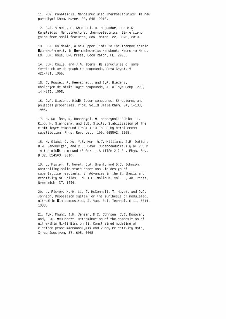
11. M.G. Kanatzidis, Nanostructured thermoelectrics: �e newparadigm? Chem. Mater. 22, 648, 2010.
12. C.J. Vineis, A. Shakouri, A. Majumdar, and M.G.Kanatzidis, Nanostructured thermoelectrics: Big e´ciencygains from small features, Adv. Mater. 22, 3970, 2010.
13. H.J. Goldsmid, A new upper limit to the thermoelectric�gure-of-merit, in �ermoelectrics Handbook: Macro to Nano,Ed. D.M. Rowe, CRC Press, Boca Raton, FL, 2006.
14. J.M. Cowley and J.A. Ibers, �e structures of someferric chloride-graphite compounds, Acta Cryst. 9,421–431, 1956.
15. J. Rouxel, A. Meerschaut, and G.A. Wiegers,Chalcogenide mis�t layer compounds, J. Alloys Comp. 229,144–157, 1995.
16. G.A. Wiegers, Mis�t layer compounds: Structures andphysical properties, Prog. Solid State Chem. 24, 1–139,1996.
17. M. Kalläne, K. Rossnagel, M. Marczynski-Bühlow, L.Kipp, H. Starnberg, and S.E. Stoltz, Stabilization of themis�t layer compound (PbS) 1.13 TaS 2 by metal crosssubstitution, Phys. Rev. Lett. 100, 065502, 2008.
18. N. Giang, Q. Xu, Y.S. Hor, A.J. Williams, S.E. Dutton,H.W. Zandbergen, and R.J. Cava, Superconductivity at 2.3 Kin the mis�t compound (PbSe) 1.16 (TiSe 2 ) 2 , Phys. Rev.B 82, 024503, 2010.
19. L. Fister, T. Novet, C.A. Grant, and D.C. Johnson,Controlling solid state reactions via design ofsuperlattice reactants, in Advances in the Synthesis andReactivity of Solids, Ed. T.E. Mallouk, Vol. 2, JAI Press,Greenwich, CT, 1994.
20. L. Fister, X.-M. Li, J. McConnell, T. Novet, and D.C.Johnson, Deposition system for the synthesis of modulated,ultrathin-�lm composites, J. Vac. Sci. Technol. A 11, 3014,1993.
21. T.M. Phung, J.M. Jensen, D.C. Johnson, J.J. Donovan,and, B.G. McBurnett, Determination of the composition ofultra-thin Ni–Si �lms on Si: Constrained modeling ofelectron probe microanalysis and x-ray re¡ectivity data,X-ray Spectrom. 37, 608, 2008.
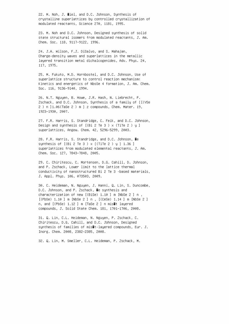
22. M. Noh, J. �iel, and D.C. Johnson, Synthesis ofcrystalline superlattices by controlled crystallization ofmodulated reactants, Science 270, 1181, 1995.
23. M. Noh and D.C. Johnson, Designed synthesis of solidstate structural isomers from modulated reactants, J. Am.Chem. Soc. 118, 9117–9122, 1996.
24. J.A. Wilson, F.J. DiSalvo, and S. Mahajan,Charge-density waves and superlattices in the metalliclayered transition metal dichalcogenides, Adv. Phys. 24,117, 1975.
25. M. Fukuto, M.D. Hornbostel, and D.C. Johnson, Use ofsuperlattice structure to control reaction mechanism:Kinetics and energetics of NbsSe 4 formation, J. Am. Chem.Soc. 116, 9136–9140, 1994.
26. N.T. Nguyen, B. Howe, J.R. Hash, N. Liebrecht, P.Zschack, and D.C. Johnson, Synthesis of a family of {[(VSe2 ) n ]1.06(TaSe 2 ) m } z compounds, Chem. Mater. 19,1923–1930, 2007.
27. F.R. Harris, S. Standridge, C. Feik, and D.C. Johnson,Design and synthesis of [(Bi 2 Te 3 ) x (TiTe 2 ) y ]superlattices, Angew. Chem. 42, 5296–5299, 2003.
28. F.R. Harris, S. Standridge, and D.C. Johnson, �esynthesis of [(Bi 2 Te 3 ) x {(TiTe 2 ) y } 1.36 ]superlattices from modulated elemental reactants, J. Am.Chem. Soc. 127, 7843–7848, 2005.
29. C. Chiritescu, C. Mortensen, D.G. Cahill, D. Johnson,and P. Zschack, Lower limit to the lattice thermalconductivity of nanostructured Bi 2 Te 3 -based materials,J. Appl. Phys. 106, 073503, 2009.
30. C. Heideman, N. Nguyen, J. Hanni, Q. Lin, S. Duncombe,D.C. Johnson, and P. Zschack, �e synthesis andcharacterization of new [(BiSe) 1.10 ] m [NbSe 2 ] n ,[(PbSe) 1.10 ] m [NbSe 2 ] n , [(CeSe) 1.14 ] m [NbSe 2 ]n, and [(PbSe) 1.12 ] m [TaSe 2 ] n mis�t layeredcompounds, J. Solid State Chem. 181, 1701–1706, 2008.
31. Q. Lin, C.L. Heideman, N. Nguyen, P. Zschack, C.Chiritescu, D.G. Cahill, and D.C. Johnson, Designedsynthesis of families of mis�t-layered compounds, Eur. J.Inorg. Chem. 2008, 2382–2385, 2008.
32. Q. Lin, M. Smeller, C.L. Heideman, P. Zschack, M.
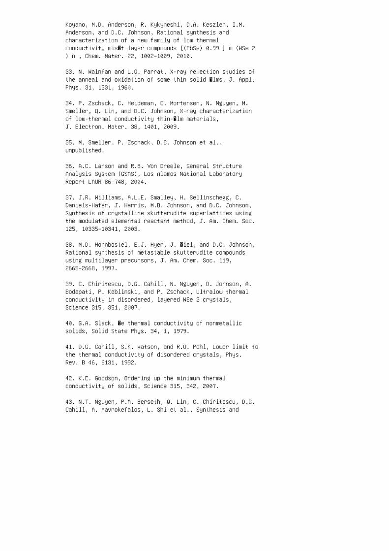
Koyano, M.D. Anderson, R. Kykyneshi, D.A. Keszler, I.M.Anderson, and D.C. Johnson, Rational synthesis andcharacterization of a new family of low thermalconductivity mis�t layer compounds [(PbSe) 0.99 ] m (WSe 2) n , Chem. Mater. 22, 1002–1009, 2010.
33. N. Wainfan and L.G. Parrat, X-ray re¡ection studies ofthe anneal and oxidation of some thin solid �lms, J. Appl.Phys. 31, 1331, 1960.
34. P. Zschack, C. Heideman, C. Mortensen, N. Nguyen, M.Smeller, Q. Lin, and D.C. Johnson, X-ray characterizationof low-thermal conductivity thin-�lm materials,J. Electron. Mater. 38, 1401, 2009.
35. M. Smeller, P. Zschack, D.C. Johnson et al.,unpublished.
36. A.C. Larson and R.B. Von Dreele, General StructureAnalysis System (GSAS), Los Alamos National LaboratoryReport LAUR 86–748, 2004.
37. J.R. Williams, A.L.E. Smalley, H. Sellinschegg, C.Daniels-Hafer, J. Harris, M.B. Johnson, and D.C. Johnson,Synthesis of crystalline skutterudite superlattices usingthe modulated elemental reactant method, J. Am. Chem. Soc.125, 10335–10341, 2003.
38. M.D. Hornbostel, E.J. Hyer, J. �iel, and D.C. Johnson,Rational synthesis of metastable skutterudite compoundsusing multilayer precursors, J. Am. Chem. Soc. 119,2665–2668, 1997.
39. C. Chiritescu, D.G. Cahill, N. Nguyen, D. Johnson, A.Bodapati, P. Keblinski, and P. Zschack, Ultralow thermalconductivity in disordered, layered WSe 2 crystals,Science 315, 351, 2007.
40. G.A. Slack, �e thermal conductivity of nonmetallicsolids, Solid State Phys. 34, 1, 1979.
41. D.G. Cahill, S.K. Watson, and R.O. Pohl, Lower limit tothe thermal conductivity of disordered crystals, Phys.Rev. B 46, 6131, 1992.
42. K.E. Goodson, Ordering up the minimum thermalconductivity of solids, Science 315, 342, 2007.
43. N.T. Nguyen, P.A. Berseth, Q. Lin, C. Chiritescu, D.G.Cahill, A. Mavrokefalos, L. Shi et al., Synthesis and
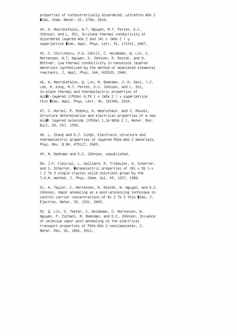
properties of turbostratically disordered, ultrathin WSe 2�lms, Chem. Mater. 22, 2750, 2010.
44. A. Mavrokefalos, N.T. Nguyen, M.T. Pettes, D.C.Johnson, and L. Shi, In-plane thermal conductivity ofdisordered layered WSe 2 and (W) x (WSe 2 ) ysuperlattice �lms, Appl. Phys. Lett. 91, 171912, 2007.
45. C. Chiritescu, D.G. Cahill, C. Heideman, Q. Lin, C.Mortensen, N.T. Nguyen, D. Johnson, R. Rostek, and H.Böttner, Low thermal conductivity in nanoscale layeredmaterials synthesized by the method of modulated elementalreactants, J. Appl. Phys. 104, 033533, 2008.
46. A. Mavrokefalos, Q. Lin, M. Beekman, J.-H. Seol, Y.J.Lee, H. Kong, M.T. Pettes, D.C. Johnson, and L. Shi,In-plane thermal and thermoelectric properties ofmis�t-layered [(PbSe) 0.99 ] x (WSe 2 ) x superlatticethin �lms, Appl. Phys. Lett. 96, 181908, 2010.
47. C. Auriel, R. Roesky, A. Meerschaut, and J. Rouxel,Structure determination and electrical properties of a newmis�t layered selenide [(PbSe) 1.10 NbSe 2 ], Mater. Res.Bull. 28, 247, 1993.
48. L. Zhang and D.J. Singh, Electronic structure andthermoelectric properties of layered PbSe-WSe 2 materials,Phys. Rev. B 80, 075117, 2009.
49. M. Beekman and D.C. Johnson, unpublished.
50. J.P. Fleurial, L. Galliard, R. Triboulet, H. Scherrer,and S. Scherrer, �ermoelectric properties of (Bi x Sb 1-x) 2 Te 3 single crystal solid solutions grown by theT.H.M. method, J. Phys. Chem. Sol. 49, 1237, 1988.
51. A. Taylor, C. Mortensen, R. Rostek, N. Nguyen, and D.C.Johnson, Vapor annealing as a post-processing technique tocontrol carrier concentrations of Bi 2 Te 3 thin �lms, J.Electron. Mater. 39, 1931, 2009.
52. Q. Lin, S. Tepfer, C. Heideman, C. Mortensen, N.Nguyen, P. Zschack, M. Beekman, and D.C. Johnson, In¡uenceof selenium vapor post-annealing on the electricaltransport properties of PbSe-WSe 2 nanolaminates, J.Mater. Res. 26, 1866, 2011.
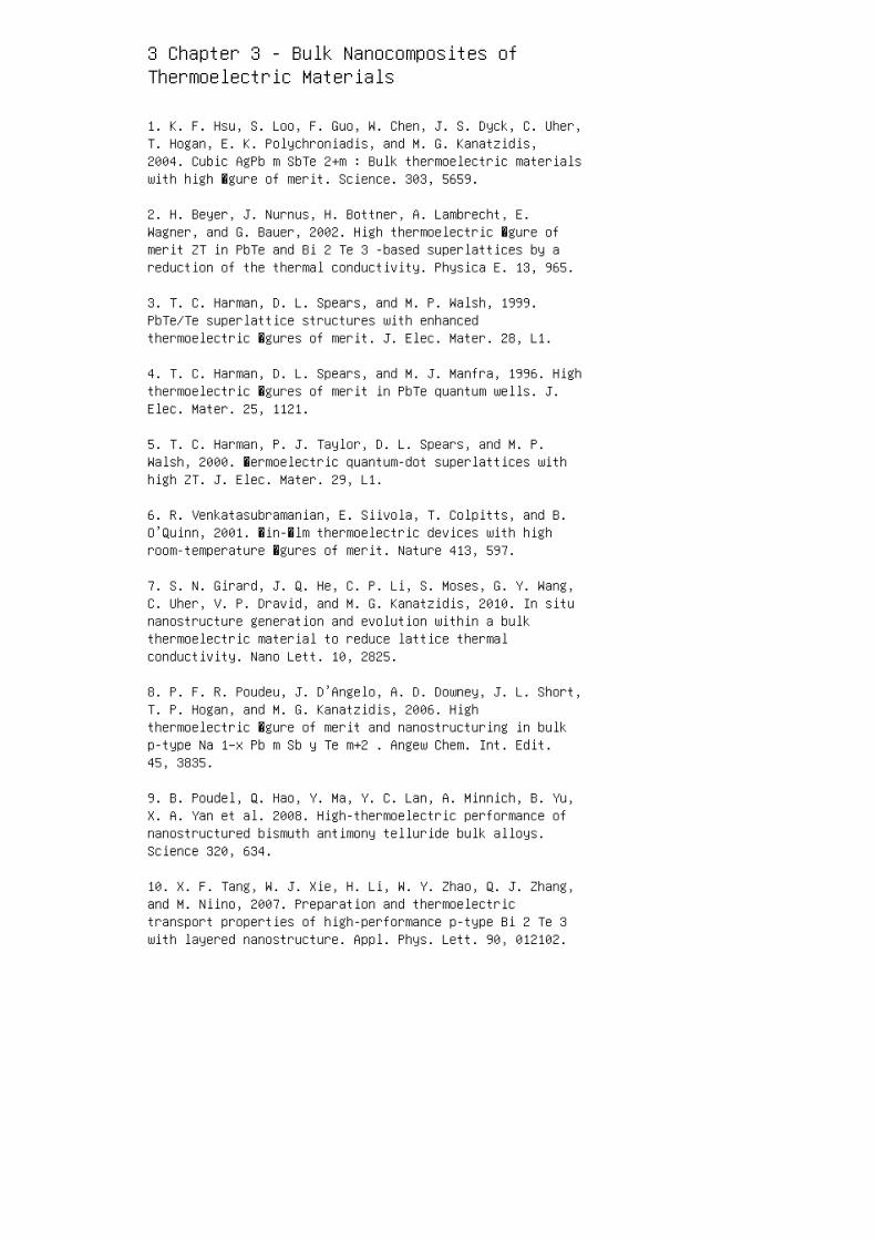
3 Chapter 3 - Bulk Nanocomposites ofThermoelectric Materials
1. K. F. Hsu, S. Loo, F. Guo, W. Chen, J. S. Dyck, C. Uher,T. Hogan, E. K. Polychroniadis, and M. G. Kanatzidis,2004. Cubic AgPb m SbTe 2+m : Bulk thermoelectric materialswith high �gure of merit. Science. 303, 5659.
2. H. Beyer, J. Nurnus, H. Bottner, A. Lambrecht, E.Wagner, and G. Bauer, 2002. High thermoelectric �gure ofmerit ZT in PbTe and Bi 2 Te 3 -based superlattices by areduction of the thermal conductivity. Physica E. 13, 965.
3. T. C. Harman, D. L. Spears, and M. P. Walsh, 1999.PbTe/Te superlattice structures with enhancedthermoelectric �gures of merit. J. Elec. Mater. 28, L1.
4. T. C. Harman, D. L. Spears, and M. J. Manfra, 1996. Highthermoelectric �gures of merit in PbTe quantum wells. J.Elec. Mater. 25, 1121.
5. T. C. Harman, P. J. Taylor, D. L. Spears, and M. P.Walsh, 2000. �ermoelectric quantum-dot superlattices withhigh ZT. J. Elec. Mater. 29, L1.
6. R. Venkatasubramanian, E. Siivola, T. Colpitts, and B.O’Quinn, 2001. �in-�lm thermoelectric devices with highroom-temperature �gures of merit. Nature 413, 597.
7. S. N. Girard, J. Q. He, C. P. Li, S. Moses, G. Y. Wang,C. Uher, V. P. Dravid, and M. G. Kanatzidis, 2010. In situnanostructure generation and evolution within a bulkthermoelectric material to reduce lattice thermalconductivity. Nano Lett. 10, 2825.
8. P. F. R. Poudeu, J. D’Angelo, A. D. Downey, J. L. Short,T. P. Hogan, and M. G. Kanatzidis, 2006. Highthermoelectric �gure of merit and nanostructuring in bulkp-type Na 1−x Pb m Sb y Te m+2 . Angew Chem. Int. Edit.45, 3835.
9. B. Poudel, Q. Hao, Y. Ma, Y. C. Lan, A. Minnich, B. Yu,X. A. Yan et al. 2008. High-thermoelectric performance ofnanostructured bismuth antimony telluride bulk alloys.Science 320, 634.
10. X. F. Tang, W. J. Xie, H. Li, W. Y. Zhao, Q. J. Zhang,and M. Niino, 2007. Preparation and thermoelectrictransport properties of high-performance p-type Bi 2 Te 3with layered nanostructure. Appl. Phys. Lett. 90, 012102.
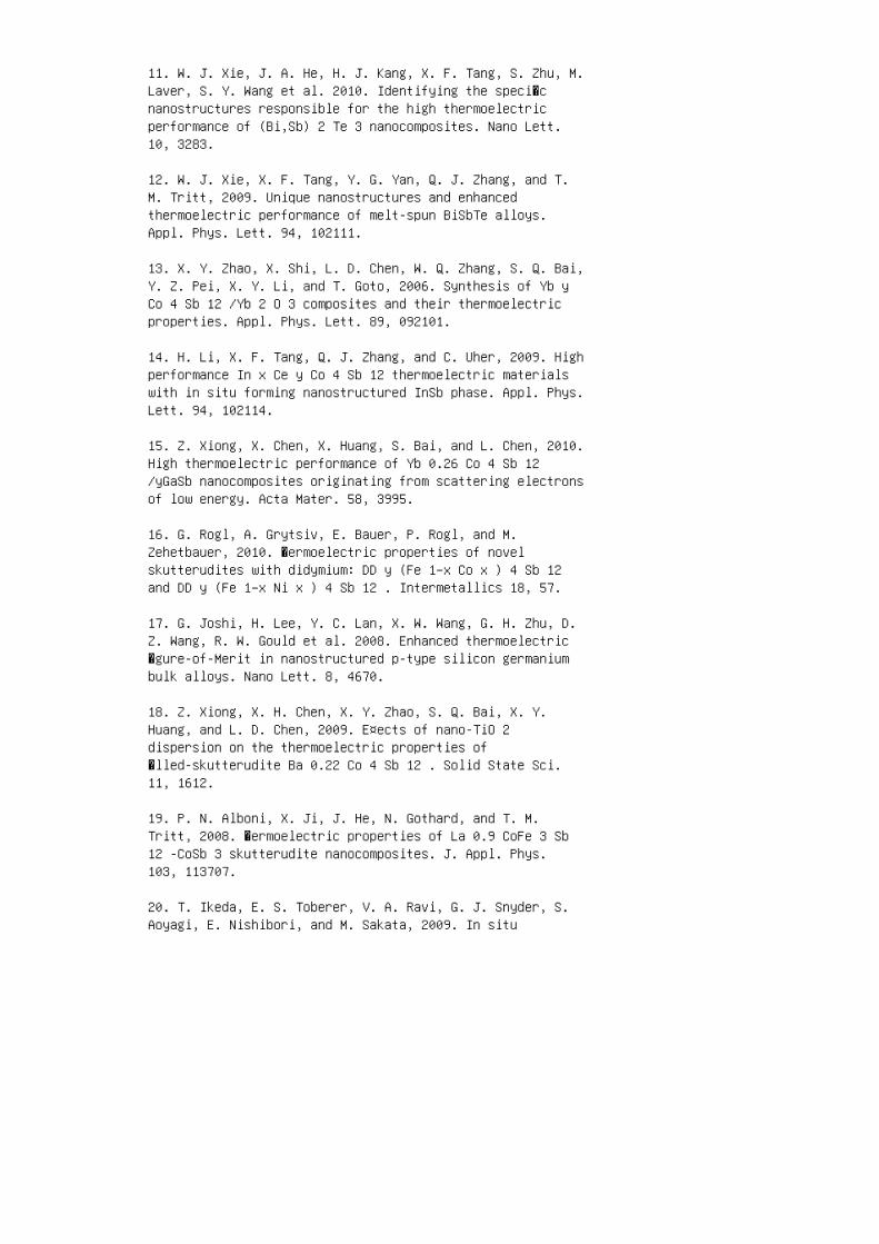
11. W. J. Xie, J. A. He, H. J. Kang, X. F. Tang, S. Zhu, M.Laver, S. Y. Wang et al. 2010. Identifying the speci�cnanostructures responsible for the high thermoelectricperformance of (Bi,Sb) 2 Te 3 nanocomposites. Nano Lett.10, 3283.
12. W. J. Xie, X. F. Tang, Y. G. Yan, Q. J. Zhang, and T.M. Tritt, 2009. Unique nanostructures and enhancedthermoelectric performance of melt-spun BiSbTe alloys.Appl. Phys. Lett. 94, 102111.
13. X. Y. Zhao, X. Shi, L. D. Chen, W. Q. Zhang, S. Q. Bai,Y. Z. Pei, X. Y. Li, and T. Goto, 2006. Synthesis of Yb yCo 4 Sb 12 /Yb 2 O 3 composites and their thermoelectricproperties. Appl. Phys. Lett. 89, 092101.
14. H. Li, X. F. Tang, Q. J. Zhang, and C. Uher, 2009. Highperformance In x Ce y Co 4 Sb 12 thermoelectric materialswith in situ forming nanostructured InSb phase. Appl. Phys.Lett. 94, 102114.
15. Z. Xiong, X. Chen, X. Huang, S. Bai, and L. Chen, 2010.High thermoelectric performance of Yb 0.26 Co 4 Sb 12/yGaSb nanocomposites originating from scattering electronsof low energy. Acta Mater. 58, 3995.
16. G. Rogl, A. Grytsiv, E. Bauer, P. Rogl, and M.Zehetbauer, 2010. �ermoelectric properties of novelskutterudites with didymium: DD y (Fe 1−x Co x ) 4 Sb 12and DD y (Fe 1−x Ni x ) 4 Sb 12 . Intermetallics 18, 57.
17. G. Joshi, H. Lee, Y. C. Lan, X. W. Wang, G. H. Zhu, D.Z. Wang, R. W. Gould et al. 2008. Enhanced thermoelectric�gure-of-Merit in nanostructured p-type silicon germaniumbulk alloys. Nano Lett. 8, 4670.
18. Z. Xiong, X. H. Chen, X. Y. Zhao, S. Q. Bai, X. Y.Huang, and L. D. Chen, 2009. E¤ects of nano-TiO 2dispersion on the thermoelectric properties of�lled-skutterudite Ba 0.22 Co 4 Sb 12 . Solid State Sci.11, 1612.
19. P. N. Alboni, X. Ji, J. He, N. Gothard, and T. M.Tritt, 2008. �ermoelectric properties of La 0.9 CoFe 3 Sb12 -CoSb 3 skutterudite nanocomposites. J. Appl. Phys.103, 113707.
20. T. Ikeda, E. S. Toberer, V. A. Ravi, G. J. Snyder, S.Aoyagi, E. Nishibori, and M. Sakata, 2009. In situ
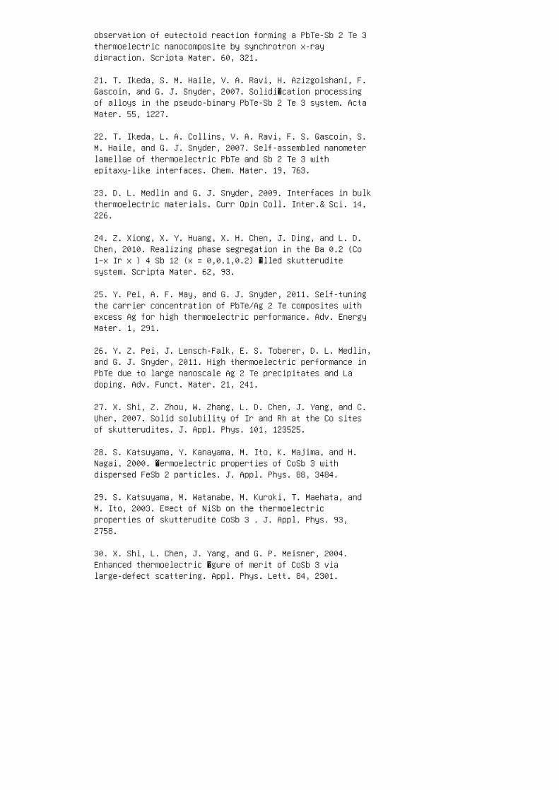
observation of eutectoid reaction forming a PbTe-Sb 2 Te 3thermoelectric nanocomposite by synchrotron x-raydi¤raction. Scripta Mater. 60, 321.
21. T. Ikeda, S. M. Haile, V. A. Ravi, H. Azizgolshani, F.Gascoin, and G. J. Snyder, 2007. Solidi�cation processingof alloys in the pseudo-binary PbTe-Sb 2 Te 3 system. ActaMater. 55, 1227.
22. T. Ikeda, L. A. Collins, V. A. Ravi, F. S. Gascoin, S.M. Haile, and G. J. Snyder, 2007. Self-assembled nanometerlamellae of thermoelectric PbTe and Sb 2 Te 3 withepitaxy-like interfaces. Chem. Mater. 19, 763.
23. D. L. Medlin and G. J. Snyder, 2009. Interfaces in bulkthermoelectric materials. Curr Opin Coll. Inter.& Sci. 14,226.
24. Z. Xiong, X. Y. Huang, X. H. Chen, J. Ding, and L. D.Chen, 2010. Realizing phase segregation in the Ba 0.2 (Co1−x Ir x ) 4 Sb 12 (x = 0,0.1,0.2) �lled skutteruditesystem. Scripta Mater. 62, 93.
25. Y. Pei, A. F. May, and G. J. Snyder, 2011. Self-tuningthe carrier concentration of PbTe/Ag 2 Te composites withexcess Ag for high thermoelectric performance. Adv. EnergyMater. 1, 291.
26. Y. Z. Pei, J. Lensch-Falk, E. S. Toberer, D. L. Medlin,and G. J. Snyder, 2011. High thermoelectric performance inPbTe due to large nanoscale Ag 2 Te precipitates and Ladoping. Adv. Funct. Mater. 21, 241.
27. X. Shi, Z. Zhou, W. Zhang, L. D. Chen, J. Yang, and C.Uher, 2007. Solid solubility of Ir and Rh at the Co sitesof skutterudites. J. Appl. Phys. 101, 123525.
28. S. Katsuyama, Y. Kanayama, M. Ito, K. Majima, and H.Nagai, 2000. �ermoelectric properties of CoSb 3 withdispersed FeSb 2 particles. J. Appl. Phys. 88, 3484.
29. S. Katsuyama, M. Watanabe, M. Kuroki, T. Maehata, andM. Ito, 2003. E¤ect of NiSb on the thermoelectricproperties of skutterudite CoSb 3 . J. Appl. Phys. 93,2758.
30. X. Shi, L. Chen, J. Yang, and G. P. Meisner, 2004.Enhanced thermoelectric �gure of merit of CoSb 3 vialarge-defect scattering. Appl. Phys. Lett. 84, 2301.
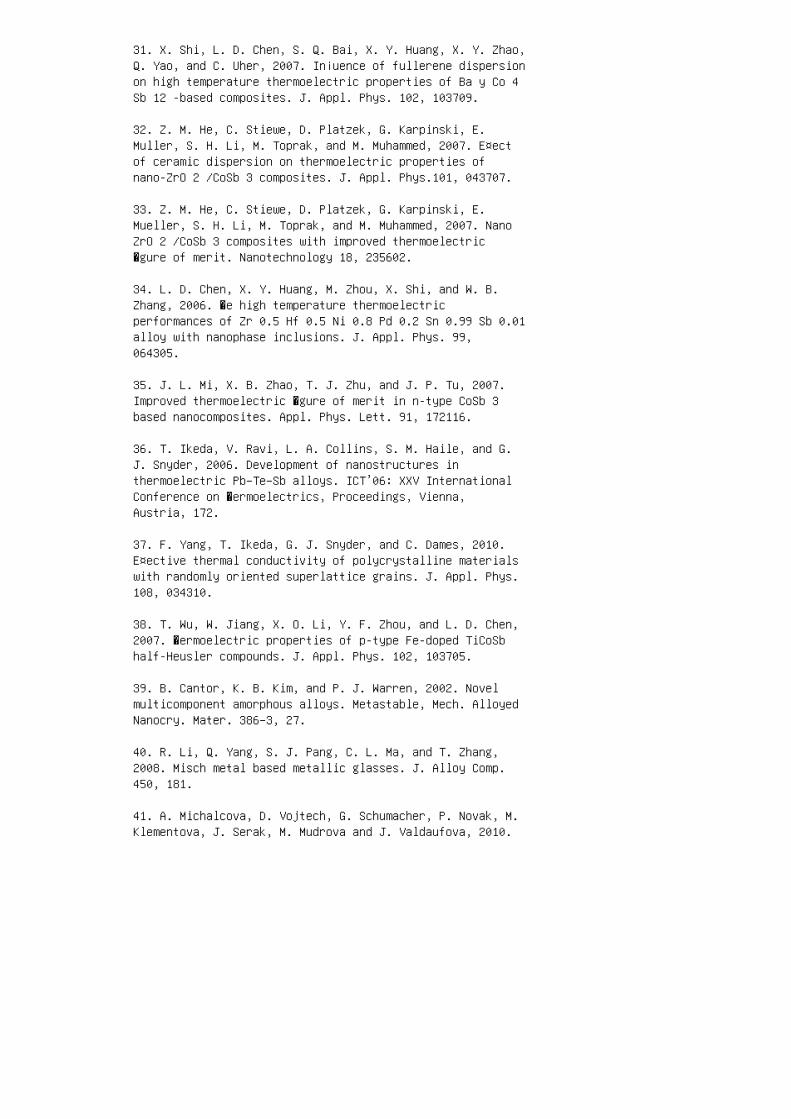
31. X. Shi, L. D. Chen, S. Q. Bai, X. Y. Huang, X. Y. Zhao,Q. Yao, and C. Uher, 2007. In¡uence of fullerene dispersionon high temperature thermoelectric properties of Ba y Co 4Sb 12 -based composites. J. Appl. Phys. 102, 103709.
32. Z. M. He, C. Stiewe, D. Platzek, G. Karpinski, E.Muller, S. H. Li, M. Toprak, and M. Muhammed, 2007. E¤ectof ceramic dispersion on thermoelectric properties ofnano-ZrO 2 /CoSb 3 composites. J. Appl. Phys.101, 043707.
33. Z. M. He, C. Stiewe, D. Platzek, G. Karpinski, E.Mueller, S. H. Li, M. Toprak, and M. Muhammed, 2007. NanoZrO 2 /CoSb 3 composites with improved thermoelectric�gure of merit. Nanotechnology 18, 235602.
34. L. D. Chen, X. Y. Huang, M. Zhou, X. Shi, and W. B.Zhang, 2006. �e high temperature thermoelectricperformances of Zr 0.5 Hf 0.5 Ni 0.8 Pd 0.2 Sn 0.99 Sb 0.01alloy with nanophase inclusions. J. Appl. Phys. 99,064305.
35. J. L. Mi, X. B. Zhao, T. J. Zhu, and J. P. Tu, 2007.Improved thermoelectric �gure of merit in n-type CoSb 3based nanocomposites. Appl. Phys. Lett. 91, 172116.
36. T. Ikeda, V. Ravi, L. A. Collins, S. M. Haile, and G.J. Snyder, 2006. Development of nanostructures inthermoelectric Pb–Te–Sb alloys. ICT’06: XXV InternationalConference on �ermoelectrics, Proceedings, Vienna,Austria, 172.
37. F. Yang, T. Ikeda, G. J. Snyder, and C. Dames, 2010.E¤ective thermal conductivity of polycrystalline materialswith randomly oriented superlattice grains. J. Appl. Phys.108, 034310.
38. T. Wu, W. Jiang, X. O. Li, Y. F. Zhou, and L. D. Chen,2007. �ermoelectric properties of p-type Fe-doped TiCoSbhalf-Heusler compounds. J. Appl. Phys. 102, 103705.
39. B. Cantor, K. B. Kim, and P. J. Warren, 2002. Novelmulticomponent amorphous alloys. Metastable, Mech. AlloyedNanocry. Mater. 386–3, 27.
40. R. Li, Q. Yang, S. J. Pang, C. L. Ma, and T. Zhang,2008. Misch metal based metallic glasses. J. Alloy Comp.450, 181.
41. A. Michalcova, D. Vojtech, G. Schumacher, P. Novak, M.Klementova, J. Serak, M. Mudrova and J. Valdaufova, 2010.
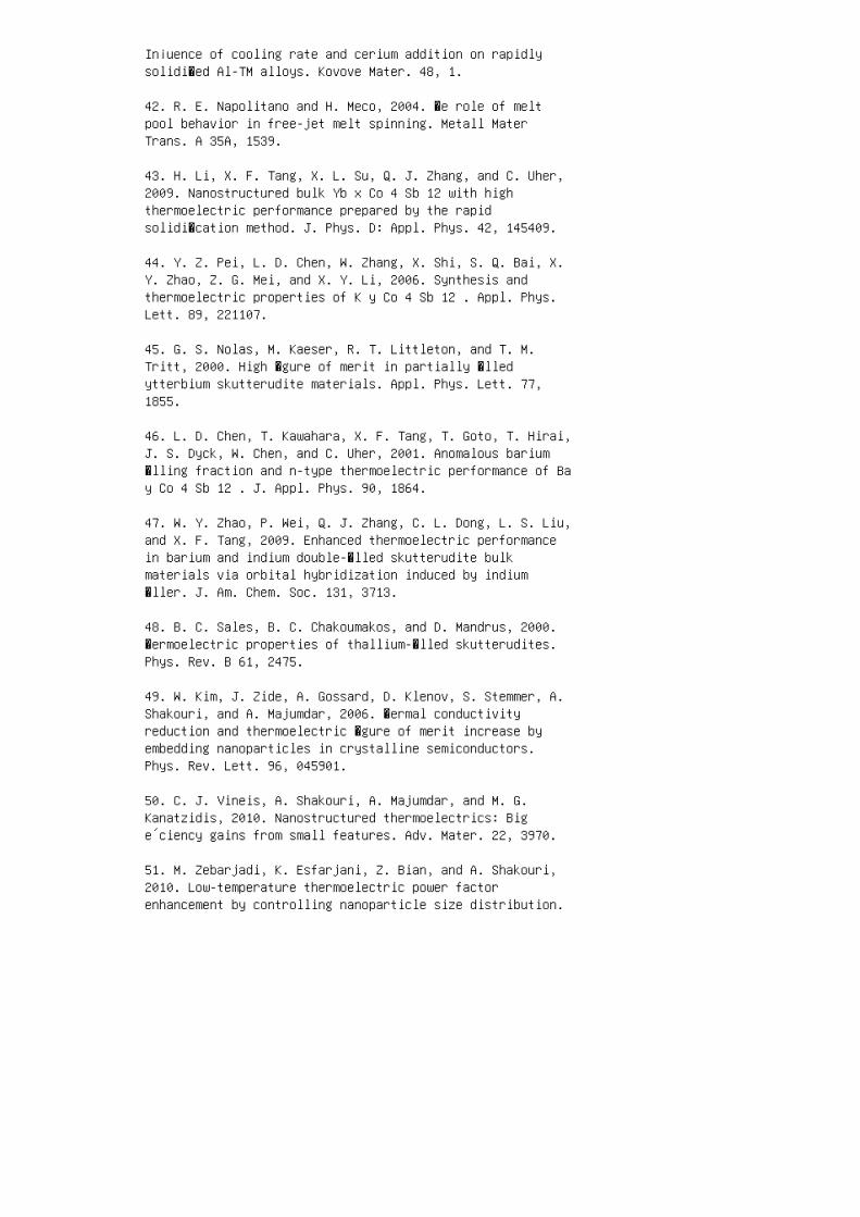
In¡uence of cooling rate and cerium addition on rapidlysolidi�ed Al-TM alloys. Kovove Mater. 48, 1.
42. R. E. Napolitano and H. Meco, 2004. �e role of meltpool behavior in free-jet melt spinning. Metall MaterTrans. A 35A, 1539.
43. H. Li, X. F. Tang, X. L. Su, Q. J. Zhang, and C. Uher,2009. Nanostructured bulk Yb x Co 4 Sb 12 with highthermoelectric performance prepared by the rapidsolidi�cation method. J. Phys. D: Appl. Phys. 42, 145409.
44. Y. Z. Pei, L. D. Chen, W. Zhang, X. Shi, S. Q. Bai, X.Y. Zhao, Z. G. Mei, and X. Y. Li, 2006. Synthesis andthermoelectric properties of K y Co 4 Sb 12 . Appl. Phys.Lett. 89, 221107.
45. G. S. Nolas, M. Kaeser, R. T. Littleton, and T. M.Tritt, 2000. High �gure of merit in partially �lledytterbium skutterudite materials. Appl. Phys. Lett. 77,1855.
46. L. D. Chen, T. Kawahara, X. F. Tang, T. Goto, T. Hirai,J. S. Dyck, W. Chen, and C. Uher, 2001. Anomalous barium�lling fraction and n-type thermoelectric performance of Bay Co 4 Sb 12 . J. Appl. Phys. 90, 1864.
47. W. Y. Zhao, P. Wei, Q. J. Zhang, C. L. Dong, L. S. Liu,and X. F. Tang, 2009. Enhanced thermoelectric performancein barium and indium double-�lled skutterudite bulkmaterials via orbital hybridization induced by indium�ller. J. Am. Chem. Soc. 131, 3713.
48. B. C. Sales, B. C. Chakoumakos, and D. Mandrus, 2000.�ermoelectric properties of thallium-�lled skutterudites.Phys. Rev. B 61, 2475.
49. W. Kim, J. Zide, A. Gossard, D. Klenov, S. Stemmer, A.Shakouri, and A. Majumdar, 2006. �ermal conductivityreduction and thermoelectric �gure of merit increase byembedding nanoparticles in crystalline semiconductors.Phys. Rev. Lett. 96, 045901.
50. C. J. Vineis, A. Shakouri, A. Majumdar, and M. G.Kanatzidis, 2010. Nanostructured thermoelectrics: Bige´ciency gains from small features. Adv. Mater. 22, 3970.
51. M. Zebarjadi, K. Esfarjani, Z. Bian, and A. Shakouri,2010. Low-temperature thermoelectric power factorenhancement by controlling nanoparticle size distribution.
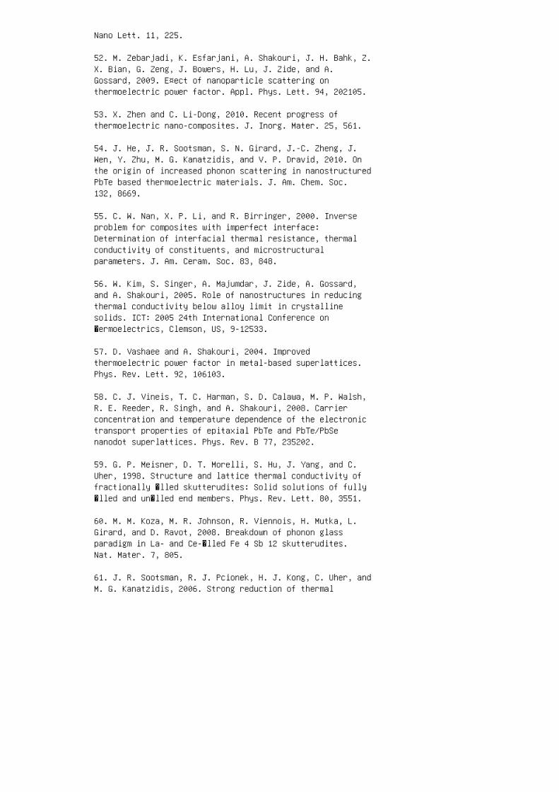
Nano Lett. 11, 225.
52. M. Zebarjadi, K. Esfarjani, A. Shakouri, J. H. Bahk, Z.X. Bian, G. Zeng, J. Bowers, H. Lu, J. Zide, and A.Gossard, 2009. E¤ect of nanoparticle scattering onthermoelectric power factor. Appl. Phys. Lett. 94, 202105.
53. X. Zhen and C. Li-Dong, 2010. Recent progress ofthermoelectric nano-composites. J. Inorg. Mater. 25, 561.
54. J. He, J. R. Sootsman, S. N. Girard, J.-C. Zheng, J.Wen, Y. Zhu, M. G. Kanatzidis, and V. P. Dravid, 2010. Onthe origin of increased phonon scattering in nanostructuredPbTe based thermoelectric materials. J. Am. Chem. Soc.132, 8669.
55. C. W. Nan, X. P. Li, and R. Birringer, 2000. Inverseproblem for composites with imperfect interface:Determination of interfacial thermal resistance, thermalconductivity of constituents, and microstructuralparameters. J. Am. Ceram. Soc. 83, 848.
56. W. Kim, S. Singer, A. Majumdar, J. Zide, A. Gossard,and A. Shakouri, 2005. Role of nanostructures in reducingthermal conductivity below alloy limit in crystallinesolids. ICT: 2005 24th International Conference on�ermoelectrics, Clemson, US, 9-12533.
57. D. Vashaee and A. Shakouri, 2004. Improvedthermoelectric power factor in metal-based superlattices.Phys. Rev. Lett. 92, 106103.
58. C. J. Vineis, T. C. Harman, S. D. Calawa, M. P. Walsh,R. E. Reeder, R. Singh, and A. Shakouri, 2008. Carrierconcentration and temperature dependence of the electronictransport properties of epitaxial PbTe and PbTe/PbSenanodot superlattices. Phys. Rev. B 77, 235202.
59. G. P. Meisner, D. T. Morelli, S. Hu, J. Yang, and C.Uher, 1998. Structure and lattice thermal conductivity offractionally �lled skutterudites: Solid solutions of fully�lled and un�lled end members. Phys. Rev. Lett. 80, 3551.
60. M. M. Koza, M. R. Johnson, R. Viennois, H. Mutka, L.Girard, and D. Ravot, 2008. Breakdown of phonon glassparadigm in La- and Ce-�lled Fe 4 Sb 12 skutterudites.Nat. Mater. 7, 805.
61. J. R. Sootsman, R. J. Pcionek, H. J. Kong, C. Uher, andM. G. Kanatzidis, 2006. Strong reduction of thermal
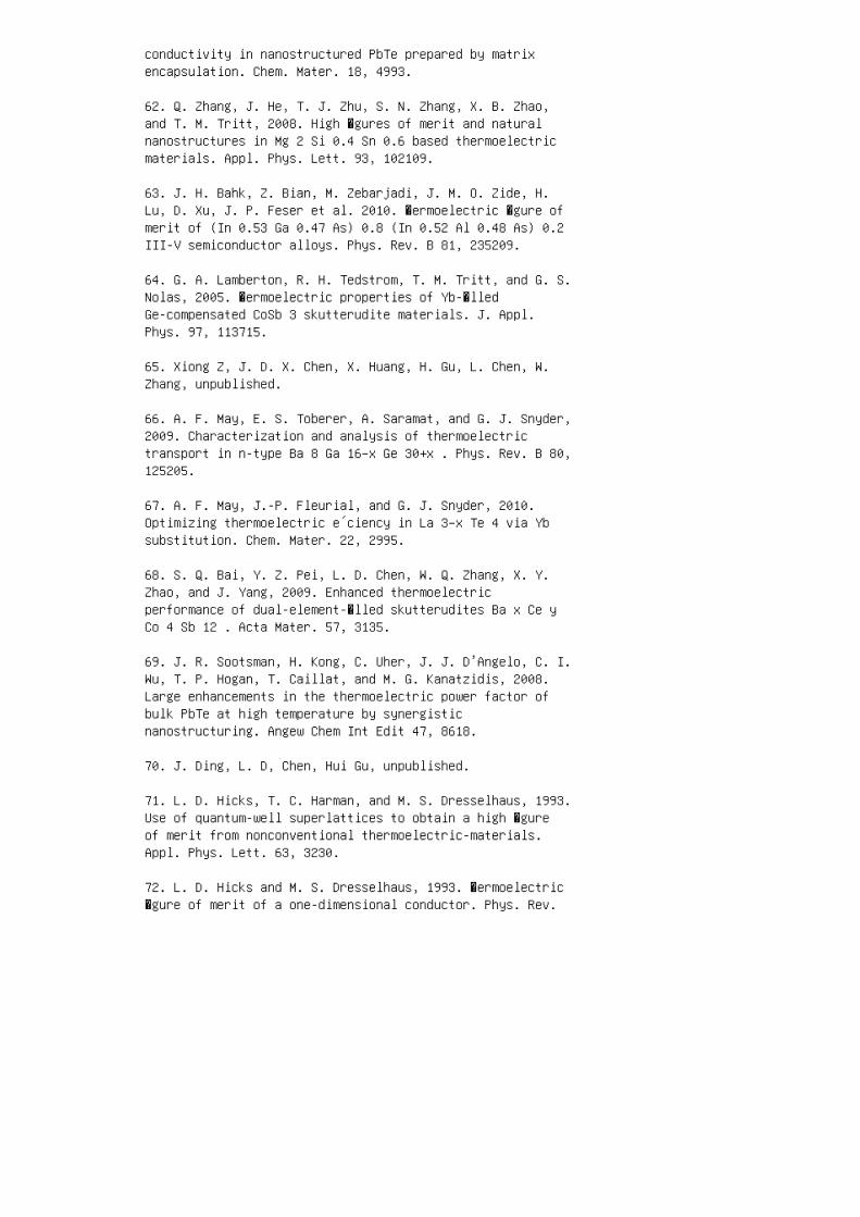
conductivity in nanostructured PbTe prepared by matrixencapsulation. Chem. Mater. 18, 4993.
62. Q. Zhang, J. He, T. J. Zhu, S. N. Zhang, X. B. Zhao,and T. M. Tritt, 2008. High �gures of merit and naturalnanostructures in Mg 2 Si 0.4 Sn 0.6 based thermoelectricmaterials. Appl. Phys. Lett. 93, 102109.
63. J. H. Bahk, Z. Bian, M. Zebarjadi, J. M. O. Zide, H.Lu, D. Xu, J. P. Feser et al. 2010. �ermoelectric �gure ofmerit of (In 0.53 Ga 0.47 As) 0.8 (In 0.52 Al 0.48 As) 0.2III-V semiconductor alloys. Phys. Rev. B 81, 235209.
64. G. A. Lamberton, R. H. Tedstrom, T. M. Tritt, and G. S.Nolas, 2005. �ermoelectric properties of Yb-�lledGe-compensated CoSb 3 skutterudite materials. J. Appl.Phys. 97, 113715.
65. Xiong Z, J. D. X. Chen, X. Huang, H. Gu, L. Chen, W.Zhang, unpublished.
66. A. F. May, E. S. Toberer, A. Saramat, and G. J. Snyder,2009. Characterization and analysis of thermoelectrictransport in n-type Ba 8 Ga 16−x Ge 30+x . Phys. Rev. B 80,125205.
67. A. F. May, J.-P. Fleurial, and G. J. Snyder, 2010.Optimizing thermoelectric e´ciency in La 3−x Te 4 via Ybsubstitution. Chem. Mater. 22, 2995.
68. S. Q. Bai, Y. Z. Pei, L. D. Chen, W. Q. Zhang, X. Y.Zhao, and J. Yang, 2009. Enhanced thermoelectricperformance of dual-element-�lled skutterudites Ba x Ce yCo 4 Sb 12 . Acta Mater. 57, 3135.
69. J. R. Sootsman, H. Kong, C. Uher, J. J. D’Angelo, C. I.Wu, T. P. Hogan, T. Caillat, and M. G. Kanatzidis, 2008.Large enhancements in the thermoelectric power factor ofbulk PbTe at high temperature by synergisticnanostructuring. Angew Chem Int Edit 47, 8618.
70. J. Ding, L. D, Chen, Hui Gu, unpublished.
71. L. D. Hicks, T. C. Harman, and M. S. Dresselhaus, 1993.Use of quantum-well superlattices to obtain a high �gureof merit from nonconventional thermoelectric-materials.Appl. Phys. Lett. 63, 3230.
72. L. D. Hicks and M. S. Dresselhaus, 1993. �ermoelectric�gure of merit of a one-dimensional conductor. Phys. Rev.

B 47, 16631.
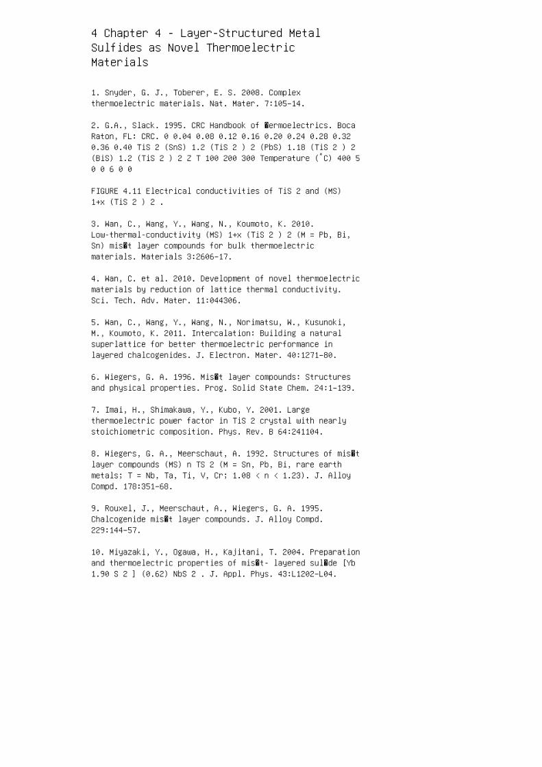
4 Chapter 4 - Layer-Structured MetalSulfides as Novel ThermoelectricMaterials
1. Snyder, G. J., Toberer, E. S. 2008. Complexthermoelectric materials. Nat. Mater. 7:105–14.
2. G.A., Slack. 1995. CRC Handbook of �ermoelectrics. BocaRaton, FL: CRC. 0 0.04 0.08 0.12 0.16 0.20 0.24 0.28 0.320.36 0.40 TiS 2 (SnS) 1.2 (TiS 2 ) 2 (PbS) 1.18 (TiS 2 ) 2(BiS) 1.2 (TiS 2 ) 2 Z T 100 200 300 Temperature (°C) 400 50 0 6 0 0
FIGURE 4.11 Electrical conductivities of TiS 2 and (MS)1+x (TiS 2 ) 2 .
3. Wan, C., Wang, Y., Wang, N., Koumoto, K. 2010.Low-thermal-conductivity (MS) 1+x (TiS 2 ) 2 (M = Pb, Bi,Sn) mis�t layer compounds for bulk thermoelectricmaterials. Materials 3:2606–17.
4. Wan, C. et al. 2010. Development of novel thermoelectricmaterials by reduction of lattice thermal conductivity.Sci. Tech. Adv. Mater. 11:044306.
5. Wan, C., Wang, Y., Wang, N., Norimatsu, W., Kusunoki,M., Koumoto, K. 2011. Intercalation: Building a naturalsuperlattice for better thermoelectric performance inlayered chalcogenides. J. Electron. Mater. 40:1271–80.
6. Wiegers, G. A. 1996. Mis�t layer compounds: Structuresand physical properties. Prog. Solid State Chem. 24:1–139.
7. Imai, H., Shimakawa, Y., Kubo, Y. 2001. Largethermoelectric power factor in TiS 2 crystal with nearlystoichiometric composition. Phys. Rev. B 64:241104.
8. Wiegers, G. A., Meerschaut, A. 1992. Structures of mis�tlayer compounds (MS) n TS 2 (M = Sn, Pb, Bi, rare earthmetals; T = Nb, Ta, Ti, V, Cr; 1.08 < n < 1.23). J. AlloyCompd. 178:351–68.
9. Rouxel, J., Meerschaut, A., Wiegers, G. A. 1995.Chalcogenide mis�t layer compounds. J. Alloy Compd.229:144–57.
10. Miyazaki, Y., Ogawa, H., Kajitani, T. 2004. Preparationand thermoelectric properties of mis�t- layered sul�de [Yb1.90 S 2 ] (0.62) NbS 2 . J. Appl. Phys. 43:L1202–L04.
11. Chiritescu, C., Cahill, D. G., Heideman, C., Lin, Q.Y., Mortensen, C., Nguyen, N. T., Johnson, D., Rostek, R.,Bottner, H. 2008. Low thermal conductivity in nanoscalelayered materials synthesized by the method of modulatedelemental reactants. J. Appl. Phys. 104:033533.
12. Heideman, C., Nyugen, N., Hanni, J., Lin, Q., Duncombe,S., Johnson, D. C., Zschack, P. 2008. �e synthesis andcharacterization of new [(BiSe) (1.10) ] (m) [NbSe 2 ] (n), [(PbSe) (1.10) ] (m) [NbSe 2 ] (n) , [(CeSe) (1.14) ] (m)[NbSe 2 ] (n) and [(PbSe) (1.12) ] (m )[TaSe 2 ] (n)mis�t layered compounds. J. Solid State Chem. 181:1701–06.
13. Lin, Q., Heideman, C. L., Nguyen, N., Zschack, P.,Chiritescu, C., Cahill, D. G., Johnson, D. C. 2008.Designed synthesis of families of mis�t-layered compounds.Eur. J. Solid State Inorg. Chem. 2008:2382–85.
14. Mavrokefalos, A., Lin, Q. Y., Beekman, M., Seol, J. H.,Lee, Y. J., Kong, H. J., Pettes, M. T., Johnson, D. C.,Shi, L. 2010. In-plane thermal and thermoelectricproperties of mis�t-layered [(PbSe) (0.99) ] (x) (WSe 2 )(x) superlattice thin �lms. Appl. Phys. Lett. 96:181908.
15. Fang, C. M., deGroot, R. A., Wiegers, G. A., Haas, C.1996. Electronic structure of the mis�t layer compound(SnS) (1.20) TiS 2 : Band structure calculations andphotoelectron spectra. J. Phys.-Condens. Mat. 8:1663–76.
16. Wiegers, G. A., Meetsma, A., Deboer, J. L., Vansmaalen,S., Haange, R. J. 1991. X-ray crystal-structuredetermination of the triclinic mis�t layer compound (SnS)1.20 TiS 2 . J. Phys.-Condens. Mat. 3:2603–12.
17. Auriel, C., Meerschaut, A., Roesky, R., Rouxel, J.1992. Crystal-structure determination andtransport-properties of a new mis�t layer compound (Pbse)1.12 (NbSe 2 ) 2 . Eur. J. Solid State Inorg. Chem.29:1079–91.
18. Meerschaut, A., Auriel, C., Rouxel, J. 1992. Structuredetermination of a new mis�t layer compound (PbS) 1.18(TiS 2 ) 2 . J. Alloy Compd. 183:129–37.
19. Meerschaut, A., Guemas, L., Auriel, C., Rouxel, J.1990. Preparation, structure determination andtransport-properties of a new mis�t layer compound—(PbS)1.14 (NbS 2 ) 2 . Eur. J. Solid State Inorg. Chem.27:557–70.
20. Klipstein, P. C., Bagnall, A. G., Liang, W. Y.,Marseglia, E. A., Friend, R. H. 1981. Stoichiometrydependence of the transport-properties of TiS 2 . J. Phys.C Solid State 14:4067–81.
21. Wilson, J. A. 1978. Modeling contrasting semimetalliccharacters of TiS 2 and TiSe 2 . Phys. Status Solidi B86:11–36.
22. Barry, J. J., Hughes, H. P., Klipstein, P. C., Friend,R. H. 1983. Stoichiometry e¤ects in angle-resolvedphotoemission and transport studies of Ti 1+X S 2 . J.Phys. C Solid State 16:393–402.
23. Meerschaut, A. 1996. Mis�t layer compounds. Curr. Opin.Solid State Mater. Sci. 1:250–59.
24. Martinez, H., Auriel, C., Gonbeau, D.,P�ster-Guillouzo, G., Meerschaut, A. 1998. Electronicstructure of two mis�t layer compounds: (PbS) (1.18) (TiS 2) and (PbS) (1.18) (TiS 2 ) (2) . J. Electron. Spectrosc.Relat. Phenom. 95:145–58.
25. Ohno, Y. 1991. Electronic-structure of the mis�t-layercompounds PbTiS 3 and SnNbS 3 . Phys. Rev. B 44:1281–91.
26. Wan, C. 2010. Unpublished data.
5 Chapter 5 - Thermoelectric Propertiesof Quantum Wires within ChrysotileAsbestos Nanotubes
1. Venkatasubramanian, R., Siivola, E., Colpitts, T., andO’Quinn, B., Nature, 413, 597–602, 2001.
2. Hsu, K.F., Loo, S., Guo, F., Chen, W., Dyck, J.S., Uher,C., Hogan, T., Polychroniadis, E.K., and Kanatzidis, M.G.,Science, 303, 818–821, 2004.
3. Harman, T.C., Walsh, M.P., Laforge, B.E., and Turner,G.W., J. Electron. Mater., 34, L19–L22, 2005.
4. Hicks, L.D. and Dresselhaus, M.S., Phys. Rev. B, 47,16631–16634, 1993.
5. Lin, Y.-M., Sun, X., and Dresselhaus, M.S., Phys. Rev.B, 62, 4610–4623, 2000.
6. Mingo, N., Appl. Phys. Lett., 84, 2652–2654, 2004(Erratum: Appl. Phys. Lett., 88, 149902, 2006).
7. Bejenari, I., Kantser, V., and Balandin A.A., Phys. Rev.B, 81, 075316, 2010.
8. Broido, D.A. and Reinecke, T.L., Phys. Rev. B, 64,045324, 2001.
9. Hochbaum, A.I., Chen, R., Delgado, R.D., Liang, W.,Garnett, E.C., Najarian, M., Majumdar, A., and Yang, P.,Nature, 451, 163–167, 2008.
10. Boukai, A.I., Bunimovich, Y., Tahir-Kheli, J., Yu,J.-K., Goddard, W.A., and Heath, J.R., Nature, 451,168–171, 2008.
11. Zhou, J., Jin, C., Seol, J.H., Li, X., and Shi, L.,Appl. Phys. Lett., 87, 133109, 2005.
12. Zhou, F., Moore, A.L., Pettes, M.T., Lee, Y., Seol,J.H., Ye, Q.L., Rabenberg, L., and Shi, L., J. Phys. D:Appl. Phys., 43, 025406, 2010.
13. Lin, Y.-M., Rabin, O., Cronin, S.B., Ying, J.Y., andDresselhaus, M.S., Appl. Phys. Lett., 81, 2403– 2405, 2002.
14. Zhou, F., Seol, J.H., Moore, A.L., Shi, L., Ye, Q.L.,and ScheÊer, R., J. Phys.: Condens. Matter, 18, 9651–9657,2006.
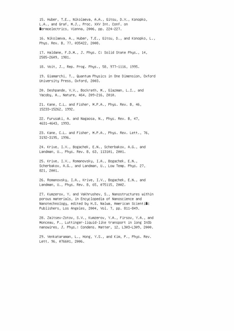
15. Huber, T.E., Nikolaeva, A.A., Gitsu, D.V., Konopko,L.A., and Graf, M.J., Proc. XXV Int. Conf. on�ermoelectrics, Vienna, 2006, pp. 224–227.
16. Nikolaeva, A., Huber, T.E., Gitsu, D., and Konopko, L.,Phys. Rev. B, 77, 035422, 2008.
17. Haldane, F.D.M., J. Phys. C: Solid State Phys., 14,2585–2609, 1981.
18. Voit, J., Rep. Prog. Phys., 58, 977–1116, 1995.
19. Giamarchi, T., Quantum Physics in One Dimension, OxfordUniversity Press, Oxford, 2003.
20. Deshpande, V.V., Bockrath, M., Glazman, L.I., andYacoby, A., Nature, 464, 209–216, 2010.
21. Kane, C.L. and Fisher, M.P.A., Phys. Rev. B, 46,15233–15262, 1992.
22. Furusaki, A. and Nagaosa, N., Phys. Rev. B, 47,4631–4643, 1993.
23. Kane, C.L. and Fisher, M.P.A., Phys. Rev. Lett., 76,3192–3195, 1996.
24. Krive, I.V., Bogachek, E.N., Scherbakov, A.G., andLandman, U., Phys. Rev. B, 63, 113101, 2001.
25. Krive, I.V., Romanovsky, I.A., Bogachek, E.N.,Scherbakov, A.G., and Landman, U., Low Temp. Phys. 27,821, 2001.
26. Romanovsky, I.A., Krive, I.V., Bogachek, E.N., andLandman, U., Phys. Rev. B, 65, 075115, 2002.
27. Kumzerov, Y. and Vakhrushev, S., Nanostructures withinporous materials, in Encyclopedia of Nanoscience andNanotechnology, edited by H.S. Nalwa, American Scienti�cPublishers, Los Angeles, 2004, Vol. 7, pp. 811–849.
28. Zaitsev-Zotov, S.V., Kumzerov, Y.A., Firsov, Y.A., andMonceau, P., Luttinger-liquid-like transport in long InSbnanowires, J. Phys.: Condens. Matter, 12, L303–L309, 2000.
29. Venkataraman, L., Hong, Y.S., and Kim, P., Phys. Rev.Lett. 96, 076601, 2006.
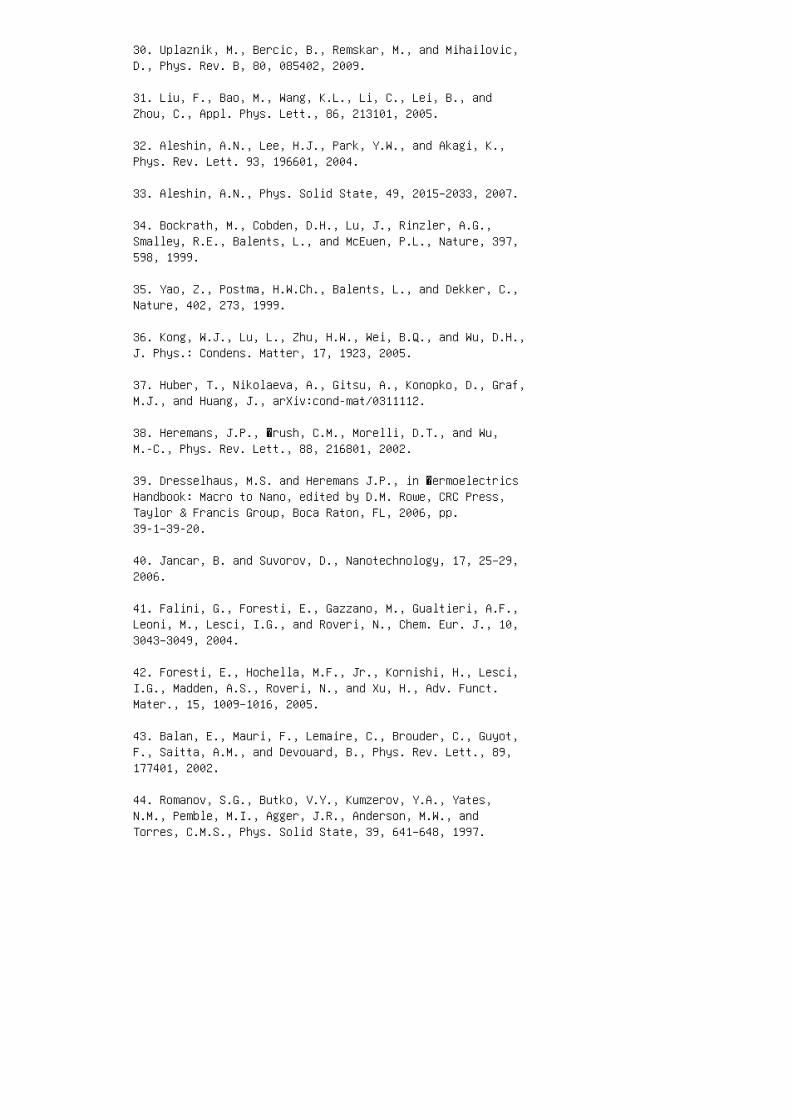
30. Uplaznik, M., Bercic, B., Remskar, M., and Mihailovic,D., Phys. Rev. B, 80, 085402, 2009.
31. Liu, F., Bao, M., Wang, K.L., Li, C., Lei, B., andZhou, C., Appl. Phys. Lett., 86, 213101, 2005.
32. Aleshin, A.N., Lee, H.J., Park, Y.W., and Akagi, K.,Phys. Rev. Lett. 93, 196601, 2004.
33. Aleshin, A.N., Phys. Solid State, 49, 2015–2033, 2007.
34. Bockrath, M., Cobden, D.H., Lu, J., Rinzler, A.G.,Smalley, R.E., Balents, L., and McEuen, P.L., Nature, 397,598, 1999.
35. Yao, Z., Postma, H.W.Ch., Balents, L., and Dekker, C.,Nature, 402, 273, 1999.
36. Kong, W.J., Lu, L., Zhu, H.W., Wei, B.Q., and Wu, D.H.,J. Phys.: Condens. Matter, 17, 1923, 2005.
37. Huber, T., Nikolaeva, A., Gitsu, A., Konopko, D., Graf,M.J., and Huang, J., arXiv:cond-mat/0311112.
38. Heremans, J.P., �rush, C.M., Morelli, D.T., and Wu,M.-C., Phys. Rev. Lett., 88, 216801, 2002.
39. Dresselhaus, M.S. and Heremans J.P., in �ermoelectricsHandbook: Macro to Nano, edited by D.M. Rowe, CRC Press,Taylor & Francis Group, Boca Raton, FL, 2006, pp.39-1–39-20.
40. Jancar, B. and Suvorov, D., Nanotechnology, 17, 25–29,2006.
41. Falini, G., Foresti, E., Gazzano, M., Gualtieri, A.F.,Leoni, M., Lesci, I.G., and Roveri, N., Chem. Eur. J., 10,3043–3049, 2004.
42. Foresti, E., Hochella, M.F., Jr., Kornishi, H., Lesci,I.G., Madden, A.S., Roveri, N., and Xu, H., Adv. Funct.Mater., 15, 1009–1016, 2005.
43. Balan, E., Mauri, F., Lemaire, C., Brouder, C., Guyot,F., Saitta, A.M., and Devouard, B., Phys. Rev. Lett., 89,177401, 2002.
44. Romanov, S.G., Butko, V.Y., Kumzerov, Y.A., Yates,N.M., Pemble, M.I., Agger, J.R., Anderson, M.W., andTorres, C.M.S., Phys. Solid State, 39, 641–648, 1997.
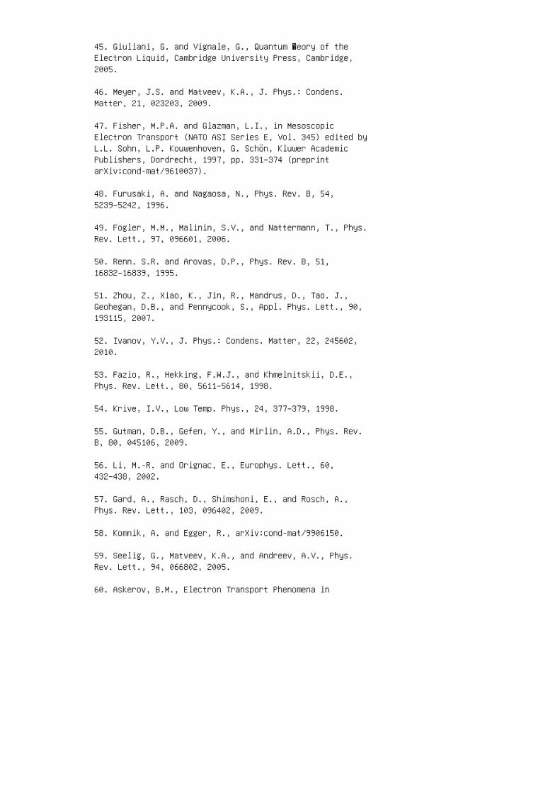
45. Giuliani, G. and Vignale, G., Quantum �eory of theElectron Liquid, Cambridge University Press, Cambridge,2005.
46. Meyer, J.S. and Matveev, K.A., J. Phys.: Condens.Matter, 21, 023203, 2009.
47. Fisher, M.P.A. and Glazman, L.I., in MesoscopicElectron Transport (NATO ASI Series E, Vol. 345) edited byL.L. Sohn, L.P. Kouwenhoven, G. Schön, Kluwer AcademicPublishers, Dordrecht, 1997, pp. 331–374 (preprintarXiv:cond-mat/9610037).
48. Furusaki, A. and Nagaosa, N., Phys. Rev. B, 54,5239–5242, 1996.
49. Fogler, M.M., Malinin, S.V., and Nattermann, T., Phys.Rev. Lett., 97, 096601, 2006.
50. Renn. S.R. and Arovas, D.P., Phys. Rev. B, 51,16832–16839, 1995.
51. Zhou, Z., Xiao, K., Jin, R., Mandrus, D., Tao. J.,Geohegan, D.B., and Pennycook, S., Appl. Phys. Lett., 90,193115, 2007.
52. Ivanov, Y.V., J. Phys.: Condens. Matter, 22, 245602,2010.
53. Fazio, R., Hekking, F.W.J., and Khmelnitskii, D.E.,Phys. Rev. Lett., 80, 5611–5614, 1998.
54. Krive, I.V., Low Temp. Phys., 24, 377–379, 1998.
55. Gutman, D.B., Gefen, Y., and Mirlin, A.D., Phys. Rev.B, 80, 045106, 2009.
56. Li, M.-R. and Orignac, E., Europhys. Lett., 60,432–438, 2002.
57. Gard, A., Rasch, D., Shimshoni, E., and Rosch, A.,Phys. Rev. Lett., 103, 096402, 2009.
58. Komnik, A. and Egger, R., arXiv:cond-mat/9906150.
59. Seelig, G., Matveev, K.A., and Andreev, A.V., Phys.Rev. Lett., 94, 066802, 2005.
60. Askerov, B.M., Electron Transport Phenomena in
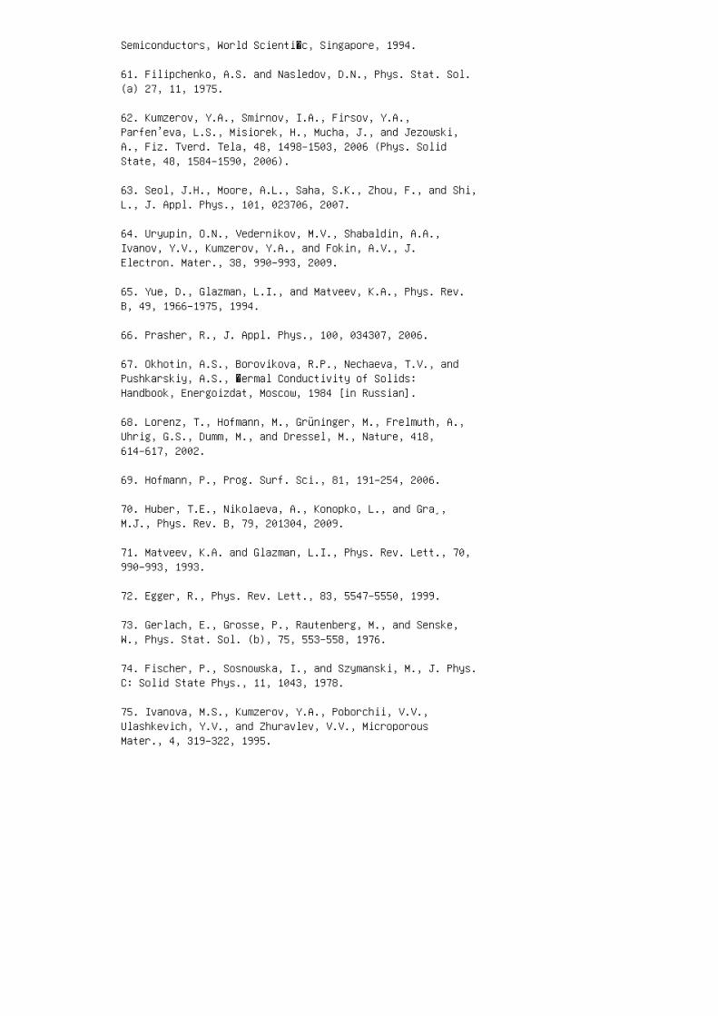
Semiconductors, World Scienti�c, Singapore, 1994.
61. Filipchenko, A.S. and Nasledov, D.N., Phys. Stat. Sol.(a) 27, 11, 1975.
62. Kumzerov, Y.A., Smirnov, I.A., Firsov, Y.A.,Parfen’eva, L.S., Misiorek, H., Mucha, J., and Jezowski,A., Fiz. Tverd. Tela, 48, 1498–1503, 2006 (Phys. SolidState, 48, 1584–1590, 2006).
63. Seol, J.H., Moore, A.L., Saha, S.K., Zhou, F., and Shi,L., J. Appl. Phys., 101, 023706, 2007.
64. Uryupin, O.N., Vedernikov, M.V., Shabaldin, A.A.,Ivanov, Y.V., Kumzerov, Y.A., and Fokin, A.V., J.Electron. Mater., 38, 990–993, 2009.
65. Yue, D., Glazman, L.I., and Matveev, K.A., Phys. Rev.B, 49, 1966–1975, 1994.
66. Prasher, R., J. Appl. Phys., 100, 034307, 2006.
67. Okhotin, A.S., Borovikova, R.P., Nechaeva, T.V., andPushkarskiy, A.S., �ermal Conductivity of Solids:Handbook, Energoizdat, Moscow, 1984 [in Russian].
68. Lorenz, T., Hofmann, M., Grüninger, M., Frelmuth, A.,Uhrig, G.S., Dumm, M., and Dressel, M., Nature, 418,614–617, 2002.
69. Hofmann, P., Prog. Surf. Sci., 81, 191–254, 2006.
70. Huber, T.E., Nikolaeva, A., Konopko, L., and Gra¸,M.J., Phys. Rev. B, 79, 201304, 2009.
71. Matveev, K.A. and Glazman, L.I., Phys. Rev. Lett., 70,990–993, 1993.
72. Egger, R., Phys. Rev. Lett., 83, 5547–5550, 1999.
73. Gerlach, E., Grosse, P., Rautenberg, M., and Senske,W., Phys. Stat. Sol. (b), 75, 553–558, 1976.
74. Fischer, P., Sosnowska, I., and Szymanski, M., J. Phys.C: Solid State Phys., 11, 1043, 1978.
75. Ivanova, M.S., Kumzerov, Y.A., Poborchii, V.V.,Ulashkevich, Y.V., and Zhuravlev, V.V., MicroporousMater., 4, 319–322, 1995.
76. Vedernikov, M.V., Uryupin, O.N., Ivanov, Y.V., andKumzerov, Y.A., Proc. 22 Int. Conf. on �ermoelectrics, LaGrande-Motte, 2003, pp. 355–358.
77. Komnik, Y. F. and Andrievskii, V.V., Fiz. Nizk. Temp.,1, 104, 1975 [Sov. J. Low Temp. Phys., 1, 51, 1975].
78. Ivanov, Y.V., Uryupin, O.N., Vedernikov, M.V.,Kumzerov, Y.A., and Fokin, A.V., in Proceedings of the XIInternational Workshop “�ermoelectrics and �eirApplications,” St. Petersburg, Russia, 2008, edited byM.V. Vedernikov (St. Petersburg, 2008), pp. 44–47 [inRussian].
79. Rabin, O., Lin, Y.-M., and Dresselhaus, M.S., Appl.Phys. Lett., 79, 81–83, 2001.
80. Höchst, H. and Ast, C.R., J. Electron Spectrosc.Related Phenomena, 137–140, 441–444, 2004.
81. Gopinathan, K.K. and Padmini, A.R.K.L., J. Phys. D:Appl. Phys., 7, 32–40, 1974.
82. Vedernikov, M.V., Uryupin, O.N., Ivanov, Y.V.,Kumzerov, Y.A., and Fokin, A.V., in Proceedings of the XInternational Workshop “�ermoelectrics and �eirApplications,” St. Petersburg, Russia, 2006, edited byM.V. Vedernikov (St. Petersburg, 2006), pp. 210–223 [inRussian].
83. Uryupin, O.N., Ivanov, Y.V., Vedernikov, M.V.,Kumzerov, Y.A., and Fokin, A.V., Proc. 3 rd Europ. Conf.on �ermoelectrics, Nancy, France, 2005, c. 35–38.
6 Chapter 6 - Bismuth Telluride Alloysfor Waste Energy Harvesting and CoolingApplications
1. Rosi, F.D., Abeles, B., and Jensen, R.V., J. Phys. Chem.Solids, 1959, 10, 191.
2. Rosi, F.D. and Ramberg, F.G. 1960. In �ermoelectricity,P.M. Egli, ed., Wiley, New York.
3. Goldsmid, H.J. 1986. �ermoelectric Refrigeration, PionLimited, London.
4. Heikes, R.R. and Ure, R.W. Jr., 1961. �ermoelectricity:Science and Engineering, Interscience, New York.
5. Rowe, D.M. and Bhandari, C.M. 1983. Modern�ermoelectrics, Holt Rinehart and Winston, London.
6. Rowe, D.M., ed. 1995. Handbook of �ermoelectrics, CRCPress, Boca Raton.
7. Satterthwaite, C.D. and Ure, R.W., Phys. Rev., 1957,108, 1164.
8. Brebrick, R.F., J. Phys. Chem. Solids, 1969, 30, 719.
9. Abrikosov, N.Kh. and Bankina, V.F., ZhNKh, 1958, 3, 659.
10. Zhukov, A.A. et al., Izvest. Akad. Nank. S.S.S.R.,Metally, 1983, 1, 183.
11. Hawlett, B., Miara, S., and Bever, M., Trans. AIME,1964, 230, 1367.
12. Abrikosov, N.Kh., Poretskaya, I.V., and Ivanova, I.P.,ZhNKh, 1959, 4, 2525.
13. Abrikosov, N.Kh. et al. Semiconductor Compounds and ItsProperties, Nauka, Moscow, 1967.
14. Boiling, G.J. Chem. Phys., 1960, 33, 305.
15. Itskevitch, E.C., Sov. Phys. J.E.T.P., 1960, 11, 255.
16. Jenkins, J.O., Rayne, J.A., and Ure, R.W., Phys. Rev.B, 1972, 5, 3171.
17. Goldsmid, H.J. 1960. Proceedings of the 5th Conferenceon Physics of Semiconductors, p. 1015, Prague.
18. Gol’tsman, B.M. et al.,1972. �ermoelectricSemiconductors Materials Based on Bi2Te3, Nauka, Moscow.
19. Boncheva, Z., Pashinkin, A.S., and Novoselova, A.V.,Neorg. Mater., 1968, 4, 291.
20. Lange, P.W., Naturwissenscha¯en, 1939, 27, 133.
21. Francombe, M.H., Br. J. Appl., 1958, 9, 415.
22. Brebrick, R.F., J. Appl. Crystallogr., 1968, 1, 241.
23. Mallinson, R.B., Rayne, J.R., and Ure, R.W. Jr., Phys.Rev., 1968, 17–5, 1049.
24. Wycko¤, R.W.G. 1964. Crystal Structures, Interscience,New York.
25. Semiletov, S.A., Kristallographiya, 1956, 1, 403.
26. Drabble, J.R. and Goodmann, C.H.I., J. Phys. Chem.Solids, 1958, 5, 142.
27. Chitroub, M., Scherrer, S., and Scherrer, H., J. Phys.Chem. Solids, 2000, 61, 1693.
28. Lovett, D.R. 1977. Semimetals and Narrow Band GapSemiconductors, Pion Limited, London.
29. Kullmann, W., Geurts, J., Richter, W. et al. Phys.Status Solidi (b), 1984, 125, 131.
30. Smith, M.J., Knight, R.J., and Spencer, C.W., J. Appl.Phys., 1962, 33, 2186.
31. Miller, G.R., Che-Yu, Li., and Spencer, C.W., J. Appl.Phys., 1973, 34, 1398.
32. Stary, Z., Horak, J., Stordeur, M., and Stölzer, M., J.Phys. Chem. Solids, 1988, 49, 97.
33. Kutasov, V.A., Svechnikova, T.E., and Chizhevskaya,S.N., Sov. Phys. Solid State, 1987, 10, 1724.
34. Birkholz, H., Z. Naturforsch, 1958, 13a, 780.
35. Stavosa, M.M. and Abrikosov, N.Kh., Jzv. An. S.S.S.R.Neorg. Mater., 1970, 6, 1090.
36. Nakajima, S.J. Phys. Chem. Solids, 1963, 24, 479.
37. Wiese, J.R. and Muldawer, L. J. Phys. Chem. Solids,1960, 15, 13.
38. O¤ergeld, G. and Van Caken Berghe, J. Nat., 1959, 10,185.
39. Pecheur, P. and Toussaint, G., J. Phys. Chem. Solids,1994, 55, 327.
40. Miller, G.R. and Che-Yu, Li., J. Phys. Chem. Solids,1965, 28, 173.
41. Przyluski, J. and Borkowski, K. 1982. Proceedings of4th Int. Conf. on �ermoelectric Energy Conversion,Arlington.
42. Sotirova, M., Sotirov, St., and Andreev, A., FreibergForschung. B, 1975, 43, 175.
43. Perrin, D., Chitroub, M., Scherrer, S., and Scherrer,H. J. Phys. Chem. Solids, 2000, 61, 1687.
44. Abrikosov, N.C. et al., Zhi. Neorg. Mater., 1981, 14,428.
45. Tamura, H., Jpn. J. Appl. Phys., 1966, 7, 593.
46. Süssmann, H., Priemuth, A., and Proehl, U. Phys. StateSolids, 1984, 82, 561.
47. Borshchevsky, A. 1995. Handbook of �ermoelectrics, D.M.Rowe ed., p. 83.
48. Scherrer, H., Weber, S., and Scherrer, S. Phys. Lett.A, 1980, 77, 189.
49. Fleurial, J.-P., Gailliard, L., Triboulet, R.,Scherrer, H., and Scherrer, S., J. Phys. Chem. Solids,1988, 49, 1237.
50. Fleurial, J.-P., Gailliard, L., Triboulet, R.,Scherrer, H., and Scherrer, S., J. Phys. Chem. Solids,1988, 49, 1249.
51. Gailliard, L., Caillat, T., Scherrer, H., and Scherrer,S. 1989, Proceedings of 8th Int. Conf. on �ermoelectricEnergy Conversion, H. Scherrer and S. Scherrer, eds., p.12, Nancy.
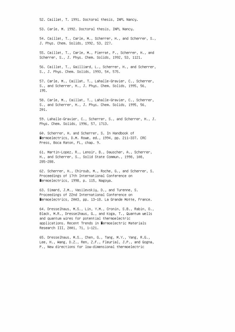
52. Caillat, T. 1991. Doctoral thesis, INPL Nancy.
53. Carle, M. 1992. Doctoral thesis, INPL Nancy.
54. Caillat, T., Carle, M., Scherrer, H., and Scherrer, S.,J. Phys. Chem. Solids, 1992, 53, 227.
55. Caillat, T., Carle, M., Pierrat, P., Scherrer, H., andScherrer, S., J. Phys. Chem. Solids, 1992, 53, 1121.
56. Caillat, T., Gailliard, L., Scherrer, H., and Scherrer,S., J. Phys. Chem. Solids, 1993, 54, 575.
57. Carle, M., Caillat, T., Lahalle-Gravier, C., Scherrer,S., and Scherrer, H., J. Phys. Chem. Solids, 1995, 56,195.
58. Carle, M., Caillat, T., Lahalle-Gravier, C., Scherrer,S., and Scherrer, H., J. Phys. Chem. Solids, 1995, 56,201.
59. Lahalle-Gravier, C., Scherrer, S., and Scherrer, H., J.Phys. Chem. Solids, 1996, 57, 1713.
60. Scherrer, H. and Scherrer, S. In Handbook of�ermoelectrics, D.M. Rowe, ed., 1994, pp. 211–337. CRCPress, Boca Raton, FL, chap. 9.
61. Martin-Lopez, R., Lenoir, B., Dauscher, A., Scherrer,H., and Scherrer, S., Solid State Commun., 1998, 108,285–288.
62. Scherrer, H., Chiroub, M., Roche, G., and Scherrer, S.Proceedings of 17th International Conference on�ermoelectrics, 1998, p. 115, Nagoya.
63. Simard, J.M., Vasilevskiy, D., and Turenne, S.Proceedings of 22nd International Conference on�ermoelectrics, 2003, pp. 13–18. La Grande Motte, France.
64. Dresselhaus, M.S., Lin, Y.M., Cronin, S.B., Rabin, O.,Black, M.R., Dresselhaus, G., and Koga, T., Quantum wellsand quantum wires for potential thermoelectricapplications. Recent Trends in �ermoelectric MaterialsResearch III, 2001, 71, 1–121.
65. Dresselhaus, M.S., Chen, G., Tang, M.Y., Yang, R.G.,Lee, H., Wang, D.Z., Ren, Z.F., Fleurial, J.P., and Gogna,P., New directions for low-dimensional thermoelectric
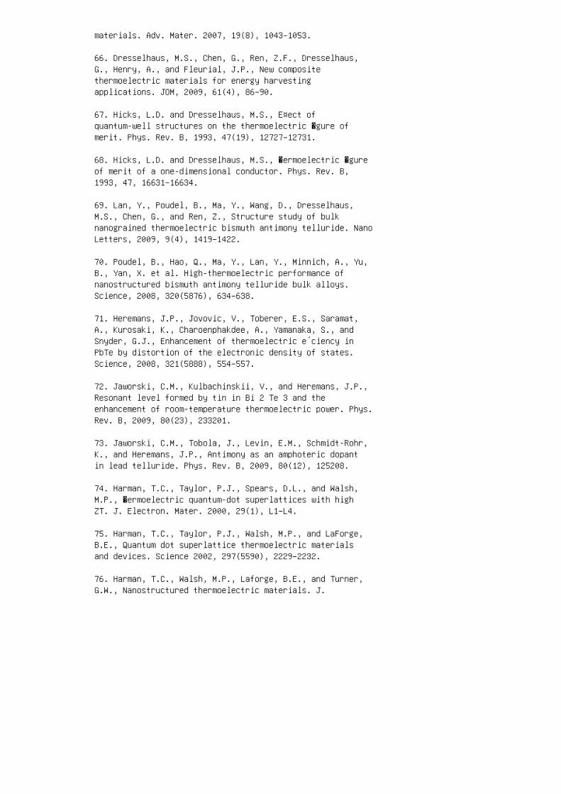
materials. Adv. Mater. 2007, 19(8), 1043–1053.
66. Dresselhaus, M.S., Chen, G., Ren, Z.F., Dresselhaus,G., Henry, A., and Fleurial, J.P., New compositethermoelectric materials for energy harvestingapplications. JOM, 2009, 61(4), 86–90.
67. Hicks, L.D. and Dresselhaus, M.S., E¤ect ofquantum-well structures on the thermoelectric �gure ofmerit. Phys. Rev. B, 1993, 47(19), 12727–12731.
68. Hicks, L.D. and Dresselhaus, M.S., �ermoelectric �gureof merit of a one-dimensional conductor. Phys. Rev. B,1993, 47, 16631–16634.
69. Lan, Y., Poudel, B., Ma, Y., Wang, D., Dresselhaus,M.S., Chen, G., and Ren, Z., Structure study of bulknanograined thermoelectric bismuth antimony telluride. NanoLetters, 2009, 9(4), 1419–1422.
70. Poudel, B., Hao, Q., Ma, Y., Lan, Y., Minnich, A., Yu,B., Yan, X. et al. High-thermoelectric performance ofnanostructured bismuth antimony telluride bulk alloys.Science, 2008, 320(5876), 634–638.
71. Heremans, J.P., Jovovic, V., Toberer, E.S., Saramat,A., Kurosaki, K., Charoenphakdee, A., Yamanaka, S., andSnyder, G.J., Enhancement of thermoelectric e´ciency inPbTe by distortion of the electronic density of states.Science, 2008, 321(5888), 554–557.
72. Jaworski, C.M., Kulbachinskii, V., and Heremans, J.P.,Resonant level formed by tin in Bi 2 Te 3 and theenhancement of room-temperature thermoelectric power. Phys.Rev. B, 2009, 80(23), 233201.
73. Jaworski, C.M., Tobola, J., Levin, E.M., Schmidt-Rohr,K., and Heremans, J.P., Antimony as an amphoteric dopantin lead telluride. Phys. Rev. B, 2009, 80(12), 125208.
74. Harman, T.C., Taylor, P.J., Spears, D.L., and Walsh,M.P., �ermoelectric quantum-dot superlattices with highZT. J. Electron. Mater. 2000, 29(1), L1–L4.
75. Harman, T.C., Taylor, P.J., Walsh, M.P., and LaForge,B.E., Quantum dot superlattice thermoelectric materialsand devices. Science 2002, 297(5590), 2229–2232.
76. Harman, T.C., Walsh, M.P., Laforge, B.E., and Turner,G.W., Nanostructured thermoelectric materials. J.
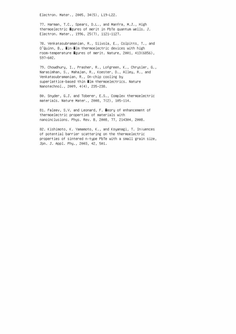
Electron. Mater., 2005, 34(5), L19–L22.
77. Harman, T.C., Spears, D.L., and Manfra, M.J., Highthermoelectric �gures of merit in PbTe quantum wells. J.Electron. Mater., 1996, 25(7), 1121–1127.
78. Venkatasubramanian, R., Siivola, E., Colpitts, T., andO’Quinn, B., �in-�lm thermoelectric devices with highroom-temperature �gures of merit. Nature, 2001, 413(6856),597–602.
79. Chowdhury, I., Prasher, R., Lofgreen, K., Chrysler, G.,Narasimhan, S., Mahajan, R., Koester, D., Alley, R., andVenkatasubramanian, R., On-chip cooling bysuperlattice-based thin �lm thermoelectrics. NatureNanotechnol., 2009, 4(4), 235–238.
80. Snyder, G.J. and Toberer, E.S., Complex thermoelectricmaterials. Nature Mater., 2008, 7(2), 105–114.
81. Faleev, S.V. and Leonard, F. �eory of enhancement ofthermoelectric properties of materials withnanoinclusions. Phys. Rev. B, 2008, 77, 214304, 2008.
82. Kishimoto, K. Yamamoto, K., and Koyanagi, T. In¡uencesof potential barrier scattering on the thermoelectricproperties of sintered n-type PbTe with a small grain size,Jpn. J. Appl. Phy., 2003, 42, 501.
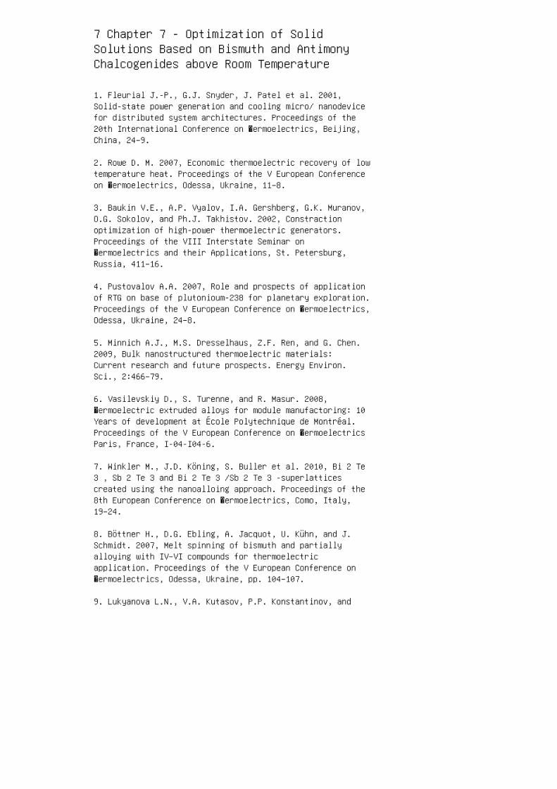
7 Chapter 7 - Optimization of SolidSolutions Based on Bismuth and AntimonyChalcogenides above Room Temperature
1. Fleurial J.-P., G.J. Snyder, J. Patel et al. 2001,Solid-state power generation and cooling micro/ nanodevicefor distributed system architectures. Proceedings of the20th International Conference on �ermoelectrics, Beijing,China, 24–9.
2. Rowe D. M. 2007, Economic thermoelectric recovery of lowtemperature heat. Proceedings of the V European Conferenceon �ermoelectrics, Odessa, Ukraine, 11–8.
3. Baukin V.E., A.P. Vyalov, I.A. Gershberg, G.K. Muranov,O.G. Sokolov, and Ph.J. Takhistov. 2002, Constractionoptimization of high-power thermoelectric generators.Proceedings of the VIII Interstate Seminar on�ermoelectrics and their Applications, St. Petersburg,Russia, 411–16.
4. Pustovalov A.A. 2007, Role and prospects of applicationof RTG on base of plutonioum-238 for planetary exploration.Proceedings of the V European Conference on �ermoelectrics,Odessa, Ukraine, 24–8.
5. Minnich A.J., M.S. Dresselhaus, Z.F. Ren, and G. Chen.2009, Bulk nanostructured thermoelectric materials:Current research and future prospects. Energy Environ.Sci., 2:466–79.
6. Vasilevskiy D., S. Turenne, and R. Masur. 2008,�ermoelectric extruded alloys for module manufactoring: 10Years of development at École Polytechnique de Montréal.Proceedings of the V European Conference on �ermoelectricsParis, France, I-04-I04-6.
7. Winkler M., J.D. Köning, S. Buller et al. 2010, Bi 2 Te3 , Sb 2 Te 3 and Bi 2 Te 3 /Sb 2 Te 3 -superlatticescreated using the nanoalloing approach. Proceedings of the8th European Conference on �ermoelectrics, Como, Italy,19–24.
8. Böttner H., D.G. Ebling, A. Jacquot, U. Kühn, and J.Schmidt. 2007, Melt spinning of bismuth and partiallyalloying with IV–VI compounds for thermoelectricapplication. Proceedings of the V European Conference on�ermoelectrics, Odessa, Ukraine, pp. 104–107.
9. Lukyanova L.N., V.A. Kutasov, P.P. Konstantinov, and
V.V. Popov. 2010, Features of the behavior of�gure-of-merit for p-type solid solutions based on bismuthand antimony chalcogenides. J. Electron. Mater.,39:2070–73.
10. Luk’yanova L.N., V.A. Kutasov, P.P. Konstantinov, andV.V. Popov. 2010, �ermoelectric �gure _ of _ merit inp-type bismuth and antimony _ chalcogenide _ based solidsolutions above room temperature. Phys. Solid State,52:1599–605 [2010, Fiz. Tverd. Tela, 52:1492–97].
11. Luk’yanova L.N., V.A. Kutasov, P.P. Konstantinov, andV.V. Popov. 2006, Speci�c features in the behavior of thee¤ective mass and mobility in n-(Bi, Sb) 2 (Te, Se, S) 3solid solutions. Phys. Solid State, 48:1856–62 [2006, Fiz.Tverd. Tela, 48:1751–56].
12. Luk’yanova L.N., V.A. Kutasov, and P.P. Konstantinov.2008, Multicomponent n-(Bi,Sb) 2 (Te,Se,S) 3 solidSolutions with di¤erent atomic substitutions in the Bi andTe sublattices. Phys. Solid State, 50:2237–44 [2008, Fiz.Tverd. Tela, 50:2143–49].
13. Luk’yanova L.N., V.A. Kutasov, and P.P. Konstantinov.2007, Solid solutions based on bismuth and antimonychalkogenides above room temperatures. Proceedings of the VEuropean Conference on �ermoelectrics. Odessa, Ukraine,pp. 172–77.
14. Luk’yanova L.N., V.A. Kutasov, P.P. Konstantinov, V.V.Popov, and G.N. Isachenko. 2007, Optimization ofmulticomponent thermoelectrics based on Bi 2 Te 3 in therange below and above room temperature. Proceedings of theXXVI International Conference on �ermoelectrics, JejuIsland, Korea, pp. 67–72.
15. Kutasov V.A. and L.N. Lukyanova. 1984, Carrier densitydependence of the e¤ective scattering parameter of solidsolutions based on bismuth telluride. Sov. Phys. SolidState, 26:1515–16 [1984, Fiz. Tverd. Tela, 26:2501–04].
16. Kutasov V.A. and L.N. Luk’yanova. 1986, Carrier densitydependence of the anisotropy parameter of n-type Bi 2 Te 3and solid solutions derived from it. Phys. Solid State,28:502–03 [1986, Fiz. Tverd. Tela. 28:899–902].
17. Luk’yanova L.N., V.A. Kutasov, V.V. Popov, and P.P.Konstantinov. 2004, Galvanomagnetic and thermoelectricproperties of p-Bi 2–x Sb x Te 3–y Se y solid solutions atlow temperatures (<220 K). Fiz. Tverd. Tela, 46:1366–71
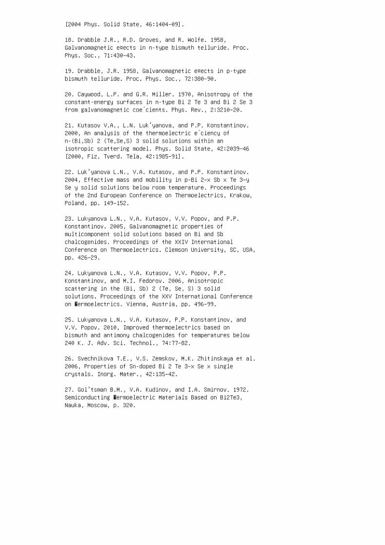
[2004 Phys. Solid State, 46:1404–09].
18. Drabble J.R., R.D. Groves, and R. Wolfe. 1958,Galvanomagnetic e¤ects in n-type bismuth telluride. Proc.Phys. Soc., 71:430–43.
19. Drabble, J.R. 1958, Galvanomagnetic e¤ects in p-typebismuth telluride. Proc. Phys. Soc., 72:380–90.
20. Caywood, L.P. and G.R. Miller. 1970, Anisotropy of theconstant-energy surfaces in n-type Bi 2 Te 3 and Bi 2 Se 3from galvanomagnetic coe´cients. Phys. Rev., 2:3210–20.
21. Kutasov V.A., L.N. Luk’yanova, and P.P. Konstantinov.2000, An analysis of the thermoelectric e´ciency ofn-(Bi,Sb) 2 (Te,Se,S) 3 solid solutions within anisotropic scattering model. Phys. Solid State, 42:2039–46[2000, Fiz. Tverd. Tela, 42:1985–91].
22. Luk’yanova L.N., V.A. Kutasov, and P.P. Konstantinov.2004, Effective mass and mobility in р-Bi 2–x Sb x Te 3–ySe y solid solutions below room temperature. Proceedingsof the 2nd European Conference on Thermoelectrics, Krakow,Poland, pp. 149–152.
23. Lukyanova L.N., V.A. Kutasov, V.V. Popov, and P.P.Konstantinov. 2005, Galvanomagnetic properties ofmulticomponent solid solutions based on Bi and Sbchalcogenides. Proceedings of the XXIV InternationalConference on Thermoelectrics. Clemson University, SC, USA,pp. 426–29.
24. Lukyanova L.N., V.A. Kutasov, V.V. Popov, P.P.Konstantinov, and M.I. Fedorov. 2006, Anisotropicscattering in the (Bi, Sb) 2 (Te, Se, S) 3 solidsolutions. Proceedings of the XXV International Conferenceon �ermoelectrics. Vienna, Austria, pp. 496–99.
25. Lukyanova L.N., V.A. Kutasov, P.P. Konstantinov, andV.V. Popov. 2010, Improved thermoelectrics based onbismuth and antimony chalcogenides for temperatures below240 K. J. Adv. Sci. Technol., 74:77–82.
26. Svechnikova T.E., V.S. Zemskov, M.K. Zhitinskaya et al.2006, Properties of Sn-doped Bi 2 Te 3–x Se x singlecrystals. Inorg. Mater., 42:135–42.
27. Gol’tsman B.M., V.A. Kudinov, and I.A. Smirnov. 1972.Semiconducting �ermoelectric Materials Based on Bi2Te3,Nauka, Moscow, p. 320.
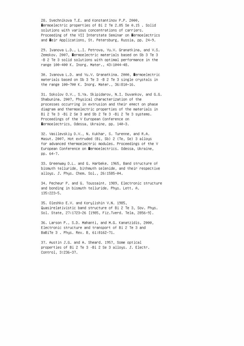
28. Svechnikova Т.Е. and Konstantinov P.P. 2000,�ermoelectric properties of Bi 2 Te 2.85 Se 0.15 . Solidsolutions with various concentrations of carriers.Proceeding of the VII Interstate Seminar on �ermoelectricsand �eir Applications, St. Petersburg, Russia, pp. 24–9.
29. Ivanova L.D., L.I. Petrova, Yu.V. Granatkina, and V.S.Zemskov. 2007, �ermoelectric materials based on Sb 3 Te 3-B 2 Te 3 solid solutions with optimal performance in therange 100–400 K. Inorg. Mater., 43:1044–48.
30. Ivanova L.D. and Yu.V. Granatkina. 2000, �ermoelectricmaterials based on Sb 3 Te 3 -B 2 Te 3 single crystals inthe range 100–700 K. Inorg. Mater., 36:810–16.
31. Sokolov O.V., S.Ya. Skipidarov, N.I. Duvankov, and G.G.Shabunina. 2007, Physical characterization of theprocesses occurring in extrusion and their e¤ect on phasediagram and thermoelectric properties of the materials inBi 2 Te 3 -Bi 2 Se 3 and Sb 2 Te 3 -Bi 2 Te 3 systems.Proceedings of the V European Conference on�ermoelectrics, Odessa, Ukraine, pp. 140–3.
32. Vasilevskiy D.V., N. Kukhar, S. Turenne, and R.A.Masut. 2007, Hot extruded (Bi, Sb) 2 (Te, Se) 3 alloysfor advanced thermoelectric modules. Proceedings of the VEuropean Conference on �ermoelectrics. Odessa, Ukraine,pp. 64–7.
33. Greenway D.L. and G. Harbeke. 1965, Band structure ofbismuth telluride, bithmuth selenide, and their respectivealloys. J. Phys. Chem. Sol., 26:1585–04.
34. Pecheur P. and G. Toussaint. 1989, Electronic structureand bonding in bismuth telluride. Phys. Lett. A.135:223–5.
35. Oleshko E.V. and Korylishin V.N. 1985,Quasirelativistic band structure of Bi 2 Te 3, Sov. Phys.Sol. State, 27:1723–26 [1985, Fiz.Tverd. Tela, 2856–9].
36. Larson P., S.D. Mahanti, and M.G. Kanatzidis, 2000,Electronic structure and transport of Bi 2 Te 3 andBaBiTe 3 . Phys. Rev. B, 61:8162–71.
37. Austin J.G. and A. Sheard. 1957, Some opticalproperties of Bi 2 Te 3 -Bi 2 Se 3 alloys. J. Electr.Control, 3:236–37.
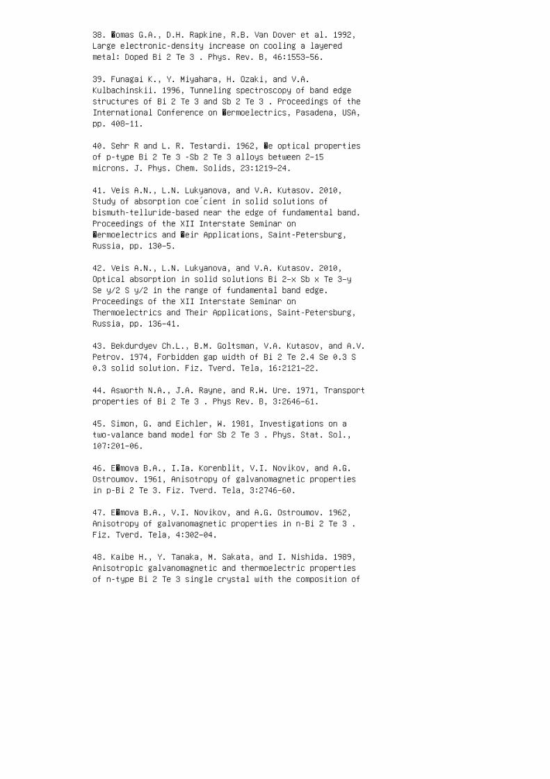
38. �omas G.A., D.H. Rapkine, R.B. Van Dover et al. 1992,Large electronic-density increase on cooling a layeredmetal: Doped Bi 2 Te 3 . Phys. Rev. B, 46:1553–56.
39. Funagai K., Y. Miyahara, H. Ozaki, and V.A.Kulbachinskii. 1996, Tunneling spectroscopy of band edgestructures of Bi 2 Te 3 and Sb 2 Te 3 . Proceedings of theInternational Conference on �ermoelectrics, Pasadena, USA,pp. 408–11.
40. Sehr R and L. R. Testardi. 1962, �e optical propertiesof p-type Bi 2 Te 3 -Sb 2 Te 3 alloys between 2–15microns. J. Phys. Chem. Solids, 23:1219–24.
41. Veis A.N., L.N. Lukyanova, and V.A. Kutasov. 2010,Study of absorption coe´cient in solid solutions ofbismuth-telluride-based near the edge of fundamental band.Proceedings of the XII Interstate Seminar on�ermoelectrics and �eir Applications, Saint-Petersburg,Russia, pp. 130–5.
42. Veis A.N., L.N. Lukyanova, and V.A. Kutasov. 2010,Optical absorption in solid solutions Bi 2–x Sb x Te 3–ySe y/2 S y/2 in the range of fundamental band edge.Proceedings of the XII Interstate Seminar onThermoelectrics and Their Applications, Saint-Petersburg,Russia, pp. 136–41.
43. Bekdurdyev Ch.L., B.M. Goltsman, V.A. Kutasov, and A.V.Petrov. 1974, Forbidden gap width of Bi 2 Te 2.4 Se 0.3 S0.3 solid solution. Fiz. Tverd. Tela, 16:2121–22.
44. Asworth N.A., J.A. Rayne, and R.W. Ure. 1971, Transportproperties of Bi 2 Te 3 . Phys Rev. B, 3:2646–61.
45. Simon, G. and Eichler, W. 1981, Investigations on atwo-valance band model for Sb 2 Te 3 . Phys. Stat. Sol.,107:201–06.
46. E�mova B.A., I.Ia. Korenblit, V.I. Novikov, and A.G.Ostroumov. 1961, Anisotropy of galvanomagnetic propertiesin p-Bi 2 Te 3. Fiz. Tverd. Tela, 3:2746–60.
47. E�mova B.A., V.I. Novikov, and A.G. Ostroumov. 1962,Anisotropy of galvanomagnetic properties in n-Bi 2 Te 3 .Fiz. Tverd. Tela, 4:302–04.
48. Kaibe H., Y. Tanaka, M. Sakata, and I. Nishida. 1989,Anisotropic galvanomagnetic and thermoelectric propertiesof n-type Bi 2 Te 3 single crystal with the composition of
a useful thermoelectric cooling material. J. Phys. Chem.Solids, 50:945–50.
49. Ohsigi I. J., T. Kojima, H. Kaibe, and I. Nishida.1989, Analysis of the anisotropic resistivities and hallcoe´cients of sintered n-type Bi 2 Te 3 Single.Proceedings of the VIII International Conference on�ermoelectrics, Nancy, France, pp. 195–99.
50. Kulbachinskii V.A., A.V.G. Kytin, and P.M. Tarasov.2006, Fermi surface and thermoelectric power of (Bi 1–x Sbx ) 2 Te 3 single crystals doped by Ag, Sn, Ga.Proceedings of the XXV International Conference on�ermoelectrics. Austria, Vienna, pp. 459–64.
51. Köhler, H. 1976, Non-parabolic E(k) relation of thelowest conduction band of Bi 2 Te 3 , Phys. Stat. Sol.(b), 73(1):95–104.
52. Köhler H., W. Haigis, and A. Middendor¤. 1976,Shubnikov-de haas investigations on n-type Bi 2 (Se x Te1–x ) 3 . Phys. Stat. Sol. (b), 78:637–42.
53. Kulbachinskii V.A., Z.M. Dashevskii, M. Inoue et al.1995, Valence-band changes in Sb 2–x In x Te 3 and Sb 2Te 3–y Se y by transport and Shubnikov de Haas e¤ectmeasurements. Phys. Rev. B, 512:10915–22.
54. Köhler H. and A. Freudenberger. 1977, Investigations ofthe highest valance band in (Bi 1–x Sb x ) 2 Te 3 crystals.Phys. Stat. Sol (b), 84:195–203.
55. Kulbachinskii V.A., A.Yu. Kaminskii, R.A. Lunin et al.2002, Quantum oscillations of Hall resistance,magnetoresistance in a magnetic �eld up to 54 T and theenergy spectrum of Sn doped layered semiconductors p-(Bi1–x Sb x ) 2 Te 3 . Semicond. Sci. Technol., 17:1133–40.
56. Müller E. and Süβmann H. 1998, Lattice thermalresistivity and two valence band model—A new understandingof transport properties of p-(Bi 1–x Sb x ) 2 Te 3 .Proceedings of the XVII International Conference on�ermoelectrics, Nagoya, Japan, pp. 85–88.
8 Chapter 8 - Effect of VacancyDistribution on the ThermoelectricProperties of Gallium and IndiumChalcogenides
1. Pei, Y., and Morelli, D. T. 2009. Vacancy phononscattering in thermoelectric In 2 Te 3 -InSb solidsolutions. Applied Physics Letters 94:122112-1.
2. Zhuze, V. P., Sergeeva, V. M., and Shelykh, A. I. 1961.Electrical properties of semiconducting In 2 Te 3 withdefective structure. Soviet Physics – Solid State 2:2545.
3. Nagat, A. T., Nassary, M. M., and El-Shaikh, H. A. 1991.Investigation of thermoelectric power of indiumsesquitelluride monocrystals. Semiconductor Science andTechnology 6:979.
4. Lakshminarayana, D., Patel, P. B., Desai, R. R., andPanchal. C. J. 2002. Investigation of thermoelectric powerin indium sesquitelluride(In 2 Te 3 ) thin �lms. Journal ofMaterials Science: Materials in Electronics 13:27.
5. Koshkin, V. M., Gal’chinetskii, L. P., and Korin, A. I.1972. Electrical conductivity of heavily doped B 2 III C 3VI semiconductors. Soviet Physics – Semiconductors 5:1718.
6. Sen, S., and Bose, D. N. 1984. Electrical and opticalproperties of single crystal In 2 Te 3 and Ga 2 Te 3 .Solid State Communications 50:39.
7. Seki, Y., Kusakabe, M., and Kashida, S. 2010. Dielectricand ac conductivity studies in as-grown Ga 2 Te 3crystals with the defect zinc-blende structure. PhysicaStatus Solidi A 207:203.
8. Desai, R. R., Lakshminarayana, D., Patel, P. B., Patel,P. K., and Panchal, C. J. 2005. Growth and structuralproperties of indium sesquitelluride (In 2 Te 3 ) thin�lms. Materials Chemistry and Physics 94:308.
9. Woolley, J. C., and Pamplin, B. R. 1959. �e orderedcrystal structure of In 2 Te 3 . Journal of the LessCommonMetals 1:362.
10. Guymont, M., Tomas, A., and Guittard, M. 1992. �estructure of Ga 2 Te 3 an x-ray and high- resolutionelectron microscopy study. Philosophical Magazine A 66:133.
11. Teraguchi, N., Kato, F., Konagai, M., Takahashi, K.,
Nakamura, Y., and Otsuka, N. 1991. Vacancy ordering of Ga2 Se 3 �lms by molecular beam epitaxy. Applied PhysicsLetters 59:567.
12. Yamanaka, S., Ishimaru, M., Charoenphakdee, A.,Matsumoto, H., and Kurosaki, K. 2009. �ermoelectriccharacterization of (Ga,In) 2 Te 3 with self-assembledtwo-dimensional vacancy planes. Journal of ElectronicMaterials 38:1392.
13. Nakamura, Y., and Hanada, T. 1997. Order-mesoscopictransition in compound semiconductor containing structuralvacancies. Electron Microsc. 32:150.
14. Ishikawa, M., and Nakayama, T. 1997. Electronicstructures of vacancy-plane-superstructured Ga 2 Te 3 andGa 2 Se 3 . Phys. Low-Dimens. Semicond. Struct. 11/12:95.
15. Zaslavskii, A. I., and Sergeeva, V. M. 1961. �epolymorphism of In 2 Te 3 . Sov. Phys. Solid State 2:2556.
16. Kurosaki, K., Matsumoto, H., Charoenphakdee, A.,Yamanaka, S., Ishimaru, M., and Hirotsu, Y. 2008.Unexpectedly low thermal conductivity in naturalnanostructured bulk Ga 2 Te 3 . Applied Physics Letters93:012101-1.
17. Kim, C. E., Kurosaki, K., Ishimaru, M., Jung, D. Y.,Muta, H., and Yamanaka, S. 2009. E¤ect of periodicity ofthe two-dimensional vacancy planes on the thermalconductivity of bulk Ga 2 Te 3 . Physica Status Solidi RRL3:221.
18. Kim, C.E., Kurosaki, K., Ishimaru, M., Muta, H., andYamanaka, S. 2011. E¤ect of vacancy distribution on thethermal conductivity of Ga 2 Te 3 and Ga 2 Se 3 . Journalof Electronic Materials 40: 999–1004.
19. Villars, P., and L.D. Calvert. 1991. Pearson’s Handbookof Crystallographic Data for Intermetallic Phases. 2nded., Materials Park, OH: ASM International.
20. Lubbers, D., and Leute, V. 1982. �e crystal structureof β-Ga 2 Se 3 . Journal of Solid State Chemistry 43:339.
9 Chapter 9 - Thermoelectric InverseClathrates
1. Rogl, P. 2006. Formation and crystal chemistry ofclathrates. In CRC Handbook of �ermoelectrics, ed. D.M.Rowe, pp. 32-1–32-24. CRC Press, Boca Raton, FL.
2. Shevelkov, A.V. 2008. Chemical aspects of the design ofthermoelectric materials. Russian Chemical Reviews 77(1):1–19.
3. Menke, H., and H. G. von Schnering. 1973. �e cagecompounds Ge 38 A 8 X 8 with A = P, As, Sb and X = Cl,Br, J. Z. Anorg. Allg. Chem. 395: 223–238.see also: 3a.Menke, H., and H. G. von Schnering. 1972. New clathratesof the type Ge 38 A 8 X 8 with A = P, As, Sb and X = Cl,Br, I. Naturwiss 59(9): 420. 3b. von Schnering, H. G., andH. Menke. 1972. Ge 38 P 8 I 8 and Ge 38 As 8 I 8 , a newclass of compounds with clathrate structure. Angew. Chemie84: 30–31.
4. Kovnir, K. A., and A. V. Shevelkov. 2004. Semiconductingclathrates: Synthesis, structure and properties. RussianChemical Reviews 73(9): 923–938.
5. Shatruk M. M., K. A. Kovnir, M. Lindsjoe, I. A.Presniakov, L. A. Kloo, and A. V. Shevelkov. 2001. Novelcompounds Sn 10 In 14 P 22 I 8 and Sn 14 In 10 P 21.2 I 8with clathrate I structure: Synthesis and crystal andelectronic structure. J. Solid State Chem. 161: 233–242.
6. Kovnir, K. A., M. M. Shatruk, L. N. Reshetova et al.2005. Novel compounds Sn 20 Zn 4 P 22-ν I 8 (ν = 1.2), Sn17 Zn 7 P 22 I 8 , and Sn 17 Zn 7 P 22 Br 8 : Synthesis,properties, and spectral features of their clathrate-likecrystal structures. Solid State Sci. 7: 957–968.
7. Falmbigl, M., P. Rogl, E. Bauer, M. Kriegisch, H.Müller, and S. Paschen. 2009. On the thermoelectricpotential of inverse clathrates. MRS Symposium Proceedings1106-N06-03.
8. Kishimoto, K., T. Koyanagi, K. Akai, and M. Matsuura.2007. Synthesis and thermoelectric properties of type-Iclathrate compounds Si 46-x P x Te 8 . Jpn. J. Appl. Phys.46: L746–L748.
9. Zaikina, J. V., K. A. Kovnir, U. Burkhardt et al. 2009.Cationic clathrate I Si 46–x P x Te y (6.6(1) ≤ y ≤7.5(1), x ≤ 2y): Crystal structure, homogeneity range, and
physical properties. Inorg. Chem. 48(8): 3720–3730.
10. Zaikina, J. V., K. A. Kovnir, U. Schwarz, H. Borrmann,and A. V. Shevelkov. 2007. Crystal structure of siliconphosphorus telluride, Si 46–x P x Te y (y = 7.35, 6.98,6.88; x ≤ 2y), a cationic clathrate-I. Z. Kristallogr. NCS222: 177–179.
11. Jaussaud, N., P. Toulemonde, M. Pouchard et al. 2004.High pressure synthesis and crystal structure of two formsof a new tellurium–silicon clathrate related to theclassical type I. Solid State Sci. 6:401–411.
12. Jaussaud, N., M. Pouchard, P. Gravereau, S. Pechev, G.Goglio, and C. Cros. 2005. Structural trends and chemicalbonding in Te-doped silicon clathrates. Inorg. Chem. 44:2210–2214.
13. Kovnir, K. A., A. N. Uglov, J. V. Zaikina, and A. V.Shevelkov. 2004. New cationic clathrate: Synthesis andstructure of [Si 40 P 6 ]I 6.5 . Mendeleev Commun. 14(4):135–136.
14. Reny, E., S. Yamanaka, C. Cros, and M. Pouchard. 2001.A new silicon clathrate compound: I 8 Si 46–x I x . AIPConference Proceedings (Nanonetwork Materials, ed. by S.Saito et al.) 590: 499–502.
15. Kishimoto, K., K. Akai, N. Muraoka, T. Koyanagi, and M.Matsuura. 2006. Synthesis and thermoelectric properties oftype-I clathrate Ge 30 P 16 Te 8 . Appl. Phys. Lett. 89:172106.
16. Menke, H., and H. G. von Schnering. 1976. �e partialsubstitution of Ge with GaAs and GaSb in the cagecompounds Ge 38 As 8 I 8 and Ge 38 Sb 8 I 8 . Z. Anorg.Allg. Chem. 424: 108–114.
17. Chu, T. L., S. S. Chu, and R. L. Ray. 1982. Germaniumarsenide iodide: A clathrate semiconductor. J. Appl. Phys.53(10): 7102–7103.
18. Ayouz, K., M. Kars, A. Rebbah, and H. Rebbah. 2009. I 8As 21 Ge 25 . Acta Crystallogr. E 65: i15.
19. Kishimoto, K., S. Arimura, and T. Koyanagi. 2006.Preparation and thermoelectric properties of sinterediodine-containing clathrate compounds Ge 38 Sb 8 I 8 andSn 38 Sb 8 I 8 . Appl. Phys. Lett. 88: 222115.
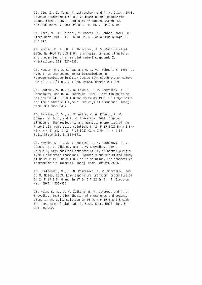
20. Jin, Z., Z. Tang, A. Litvinchuk, and A. M. Guloy. 2008.Inverse clathrate with a signi�cant nonstoichiometriccompositional range. Abstracts of Papers, 235th ACSNational Meeting, New Orleans, LA, USA, April 6–10.
21. Kars, M., T. Roisnel, V. Dorcet, A. Rebbah, and L. C.Otero-Diaz. 2010. I 8 Sb 10 Ge 36 . Acta Crystallogr. E66: i47.
22. Kovnir, K. A., N. S. Abramchuk, J. V. Zaikina et al.2006. Ge 40.0 Te 5.3 I 8 : Synthesis, crystal structure,and properties of a new clathrate-I compound. Z.Kristallogr. 221: 527–532.
23. Nesper, R., J. Curda, and H. G. von Schnering. 1986. Ge4.06 I, an unexpected germaniumsubiodide— Atetragermanioiodonium(III)-iodide with clathrate structure[Ge 46–x I x ]I 8 , x = 8/3. Angew. Chemie 25: 369.
24. Shatruk, M. M., K. A. Kovnir, A. V. Shevelkov, I. A.Presniakov, and B. A. Popovkin. 1999. First tin pnictidehalides Sn 24 P 19.3 I 8 and Sn 24 As 19.3 I 8 : Synthesisand the clathrate-I type of the crystal structure. Inorg.Chem. 38: 3455–3457.
25. Zaikina, J. V., W. Schnelle, K. A. Kovnir, A. V.Olenev, Y. Grin, and A. V. Shevelkov. 2007. Crystalstructure, thermoelectric and magnetic properties of thetype-I clathrate solid solutions Sn 24 P 19.3(2) Br x I 8–x(0 ≤ x ≤ 8) and Sn 24 P 19.3(2) Cl y I 8–y (y ≤ 0.8).Solid State Sci. 9: 664–671.
26. Kovnir, K. A., J. V. Zaikina, L. N. Reshetova, A. V.Olenev, E. V. Dikarev, and A. V. Shevelkov. 2004.Unusually high chemical compressibility of normally rigidtype-I clathrate framework: Synthesis and structural studyof Sn 24 P 19.3 Br x I 8–x solid solution, the prospectivethermoelectric material. Inorg. Chem. 43:3230–3236.
27. Stefanoski, S., L. N. Reshetova, A. V. Shevelkov, andG. S. Nolas. 2009. Low-temperature transport properties ofSn 24 P 19.3 Br 8 and Sn 17 Zn 7 P 22 Br 8 . J. Electron.Mat. 38(7): 985–989.
28. Kelm, E. A., J. V. Zaikina, E. V. Dikarev, and A. V.Shevelkov. 2009. Distribution of phosphorus and arsenicatoms in the solid solution Sn 24 As x P 19.3–x I 8 withthe structure of clathrate-I. Russ. Chem. Bull. Int. Ed.58: 746–750.
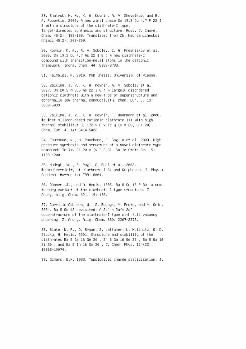
29. Shatruk, M. M., K. A. Kovnir, A. V. Shevelkov, and B.A. Popovkin. 2000. A new zintl phase Sn 19.3 Cu 4.7 P 22 I8 with a structure of the clathrate-I type:Target-directed synthesis and structure. Russ. J. Inorg.Chem. 45(2): 153–159. Translated from Zh. NeorganicheskoiKhimii 45(2): 203–209.
30. Kovnir, K. A., A. V. Sobolev, I. A. Presniakov et al.2005. Sn 19.3 Cu 4.7 As 22 I 8 : A new clathrate-Icompound with transition-metal atoms in the cationicframework. Inorg. Chem. 44: 8786–8793.
31. Falmbigl, M. 2010. PhD thesis, University of Vienna.
32. Zaikina, J. V., K. A. Kovnir, A. V. Sobolev et al.2007. Sn 20.5 □ 3.5 As 22 I 8 : A largely disorderedcationic clathrate with a new type of superstructure andabnormally low thermal conductivity. Chem. Eur. J. 13:5090–5099.
33. Zaikina, J. V., K. A. Kovnir, F. Haarmann et al. 2008.�e �rst silicon-based cationic clathrate III with highthermal stability: Si 172–x P x Te y (x = 2y, y > 20).Chem. Eur. J. 14: 5414–5422.
34. Jaussaud, N., M. Pouchard, G. Goglio et al. 2003. Highpressure synthesis and structure of a novel clathrate-typecompound: Te 7+x Si 20–x (x ~ 2.5). Solid State Sci. 5:1193–1200.
35. Mudryk, Ya., P. Rogl, C. Paul et al. 2002.�ermoelectricity of clathrate I Si and Ge phases. J. Phys.:Condens. Matter 14: 7991–8004.
36. Dünner, J., and A. Mewis. 1995. Ba 8 Cu 16 P 30 -a newternary variant of the clathrate I-type structure. Z.Anorg. Allg. Chem. 621: 191–196.
37. Carrillo-Cabrera, W., S. Budnyk, Y. Prots, and Y. Grin.2004. Ba 8 Ge 43 revisited: A 2a′ × 2a′× 2a′superstructure of the clathrate-I type with full vacancyordering. Z. Anorg. Allg. Chem. 630: 2267–2276.
38. Blake, N. P., D. Bryan, S. Lattumer, L. Mollnitz, G. D.Stucky, H. Metiu. 2001. Structure and stability of theclathrates Ba 8 Ga 16 Ge 30 , Sr 8 Ga 16 Ge 30 , Ba 8 Ga 16Si 30 , and Ba 8 In 16 Sn 30 . J. Chem. Phys. 114(22):10063–10074.
39. Gimarc, B.M. 1983. Topological charge stabilisation. J.
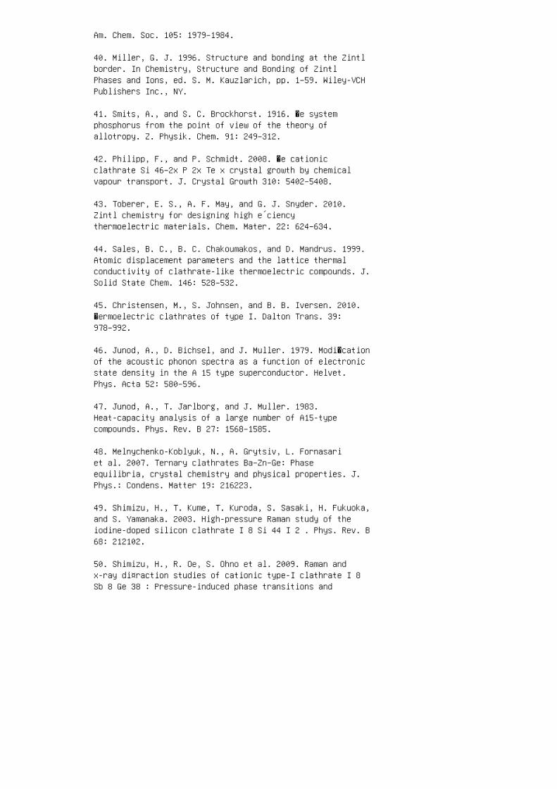
Am. Chem. Soc. 105: 1979–1984.
40. Miller, G. J. 1996. Structure and bonding at the Zintlborder. In Chemistry, Structure and Bonding of ZintlPhases and Ions, ed. S. M. Kauzlarich, pp. 1–59. Wiley-VCHPublishers Inc., NY.
41. Smits, A., and S. C. Brockhorst. 1916. �e systemphosphorus from the point of view of the theory ofallotropy. Z. Physik. Chem. 91: 249–312.
42. Philipp, F., and P. Schmidt. 2008. �e cationicclathrate Si 46–2x P 2x Te x crystal growth by chemicalvapour transport. J. Crystal Growth 310: 5402–5408.
43. Toberer, E. S., A. F. May, and G. J. Snyder. 2010.Zintl chemistry for designing high e´ciencythermoelectric materials. Chem. Mater. 22: 624–634.
44. Sales, B. C., B. C. Chakoumakos, and D. Mandrus. 1999.Atomic displacement parameters and the lattice thermalconductivity of clathrate-like thermoelectric compounds. J.Solid State Chem. 146: 528–532.
45. Christensen, M., S. Johnsen, and B. B. Iversen. 2010.�ermoelectric clathrates of type I. Dalton Trans. 39:978–992.
46. Junod, A., D. Bichsel, and J. Muller. 1979. Modi�cationof the acoustic phonon spectra as a function of electronicstate density in the A 15 type superconductor. Helvet.Phys. Acta 52: 580–596.
47. Junod, A., T. Jarlborg, and J. Muller. 1983.Heat-capacity analysis of a large number of A15-typecompounds. Phys. Rev. B 27: 1568–1585.
48. Melnychenko-Koblyuk, N., A. Grytsiv, L. Fornasariet al. 2007. Ternary clathrates Ba–Zn–Ge: Phaseequilibria, crystal chemistry and physical properties. J.Phys.: Condens. Matter 19: 216223.
49. Shimizu, H., T. Kume, T. Kuroda, S. Sasaki, H. Fukuoka,and S. Yamanaka. 2003. High-pressure Raman study of theiodine-doped silicon clathrate I 8 Si 44 I 2 . Phys. Rev. B68: 212102.
50. Shimizu, H., R. Oe, S. Ohno et al. 2009. Raman andx-ray di¤raction studies of cationic type-I clathrate I 8Sb 8 Ge 38 : Pressure-induced phase transitions and
amorphization. J. Appl. Phys. 105: 043522.
51. Reny, E., A. San Miguel, Y. Guyot et al. 2002.Vibrational modes in silicon clathrate compounds: A key tounderstanding superconductivity. Phys. Rev. B 66: 014532.
52. Yakimchuk, A.V., J. V. Zaikina, L. N. Reshetova, L. I.Ryabova, D. R. Khokhlov, and A. V. Shevelkov. 2007.Impedance of Sn 24 P 19.3 Br x I 8–x semiconductingclathrates. Low Temp. Phys. 33(2–3): 276–279.
53. Toberer, E. S., M. Christensen, B. B. Iversen, and G.J. Snyder. 2008. High temperature thermoelectric e´ciencyin Ba 8 Ga 16 Ge 30 . Phys. Rev. B 77: 075203.
54. Cahill, D. G., and R. O. Pohl. 1989. Heat ¡ow andlattice vibrations in glasses. Solid State Commun.70:927–930.
55. Nolas, G. S., B. C. Chakoumakos, B. Mahieu, G. J. Long,and T. J. R. Weakley. 2000. Structural characterizationand thermal conductivity of type-I tin clathrates. Chem.Mater. 12: 1947–1953.
56. San Miguel, A., P. Melinon, D. Connetable et al. 2002.Pressure stability and low compressibility of intercalatedcagelike materials: �e case of silicon clathrates. Phys.Rev. B 65: 054109.
57. Connetable, D. 2007. Structural and electronicproperties of p-doped silicon clathrates. Phys. Rev. B 75:125202.
58. Connetable, D., V. Timoshevskii, E. Artacho, and X.Blase. 2001. Tailoring band gap and hardness byintercalation: An ab initio study of I8@Si-46 and relateddoped clathrates. Phys. Rev. Letters 87(20): 206405.
59. San Miguel, A., A. Merlen, P. Toulemonde et al. 2005.Pressure-induced homothetic volume collapse in siliconclathrates. Europhys. Lett. 69(4): 556–562.
60. Paschen, S., V. H. Tran, M. Baenitz, W.Carrillo-Cabrera, Yu. Grin, and F. Steglich. 2002.Clathrate Ba 6 Ge 25 : �ermodynamic, magnetic, andtransport properties. Phys. Rev. B 65: 134435.
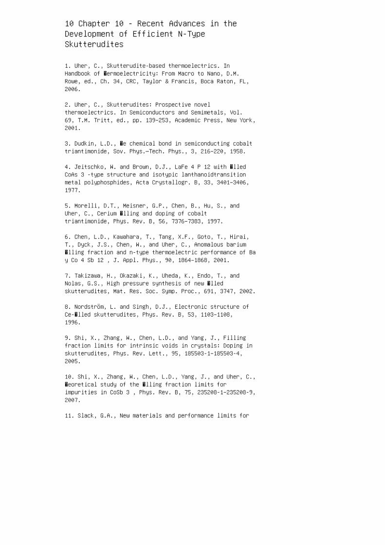
10 Chapter 10 - Recent Advances in theDevelopment of Efficient N-TypeSkutterudites
1. Uher, C., Skutterudite-based thermoelectrics. InHandbook of �ermoelectricity: From Macro to Nano, D.M.Rowe, ed., Ch. 34, CRC, Taylor & Francis, Boca Raton, FL,2006.
2. Uher, C., Skutterudites: Prospective novelthermoelectrics. In Semiconductors and Semimetals, Vol.69, T.M. Tritt, ed., pp. 139–253, Academic Press, New York,2001.
3. Dudkin, L.D., �e chemical bond in semiconducting cobalttriantimonide, Sov. Phys.—Tech. Phys., 3, 216–220, 1958.
4. Jeitschko, W. and Brown, D.J., LaFe 4 P 12 with �lledCoAs 3 -type structure and isotypic lanthanoidtransitionmetal polyphosphides, Acta Crystallogr. B, 33, 3401–3406,1977.
5. Morelli, D.T., Meisner, G.P., Chen, B., Hu, S., andUher, C., Cerium �lling and doping of cobalttriantimonide, Phys. Rev. B, 56, 7376–7383, 1997.
6. Chen, L.D., Kawahara, T., Tang, X.F., Goto, T., Hirai,T., Dyck, J.S., Chen, W., and Uher, C., Anomalous barium�lling fraction and n-type thermoelectric performance of Bay Co 4 Sb 12 , J. Appl. Phys., 90, 1864–1868, 2001.
7. Takizawa, H., Okazaki, K., Uheda, K., Endo, T., andNolas, G.S., High pressure synthesis of new �lledskutterudites, Mat. Res. Soc. Symp. Proc., 691, 3747, 2002.
8. Nordström, L. and Singh, D.J., Electronic structure ofCe-�lled skutterudites, Phys. Rev. B, 53, 1103–1108,1996.
9. Shi, X., Zhang, W., Chen, L.D., and Yang, J., Fillingfraction limits for intrinsic voids in crystals: Doping inskutterudites, Phys. Rev. Lett., 95, 185503-1–185503-4,2005.
10. Shi, X., Zhang, W., Chen, L.D., Yang, J., and Uher, C.,�eoretical study of the �lling fraction limits forimpurities in CoSb 3 , Phys. Rev. B, 75, 235208-1–235208-9,2007.
11. Slack, G.A., New materials and performance limits for
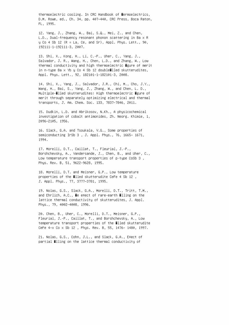
thermoelectric cooling. In CRC Handbook of �ermoelectrics,D.M. Rowe, ed., Ch. 34, pp. 407–440, CRC Press, Boca Raton,FL, 1995.
12. Yang, J., Zhang, W., Bai, S.Q., Mei, Z., and Chen,L.D., Dual-frequency resonant phonon scattering in Ba x Ry Co 4 Sb 12 (R = La, Ce, and Sr), Appl. Phys. Lett., 90,192111-1–192111-3, 2007.
13. Shi, X., Kong, H., Li, C.-P., Uher, C., Yang, J.,Salvador, J. R., Wang, H., Chen, L.D., and Zhang, W., Lowthermal conductivity and high thermoelectric �gure of meritin n-type Ba x Yb y Co 4 Sb 12 double�lled skutterudites,Appl. Phys. Lett., 92, 182101–1–182101-3, 2008.
14. Shi, X., Yang, J., Salvador, J.R., Chi, M., Cho, J.Y.,Wang, H., Bai, S., Yang, J., Zhang, W., and Chen, L. D.,Multiple-�lled skutterudites: High thermoelectric �gure ofmerit through separately optimizing electrical and thermaltransports, J. Am. Chem. Soc. 133, 7837–7846, 2011.
15. Dudkin, L.D. and Abrikosov, N.Kh., A physicochemicalinvestigation of cobalt antimonides, Zh. Neorg. Khimie, 1,2096–2105, 1956.
16. Slack, G.A. and Tsoukala, V.G., Some properties ofsemiconducting IrSb 3 , J. Appl. Phys., 76, 1665– 1671,1994.
17. Morelli, D.T., Caillat, T., Fleurial, J.-P.,Borshchevsky, A., Vandersande, J., Chen, B., and Uher, C.,Low temperature transport properties of p-type CoSb 3 ,Phys. Rev. B, 51, 9622–9628, 1995.
18. Morelli, D.T. and Meisner, G.P., Low temperatureproperties of the �lled skutterudite CeFe 4 Sb 12 ,J. Appl. Phys., 77, 3777–3781, 1995.
19. Nolas, G.S., Slack, G.A., Morelli, D.T., Tritt, T.M.,and Ehrlich, A.C., �e e¤ect of rare-earth �lling on thelattice thermal conductivity of skutterudites, J. Appl.Phys., 79, 4002–4008, 1996.
20. Chen, B., Uher, C., Morelli, D.T., Meisner, G.P.,Fleurial, J.-P., Caillat, T., and Borshchevsky, A., Lowtemperature transport properties of the �lled skutteruditeCeFe 4–x Co x Sb 12 , Phys. Rev. B, 55, 1476– 1480, 1997.
21. Nolas, G.S., Cohn, J.L., and Slack, G.A., E¤ect ofpartial �lling on the lattice thermal conductivity of
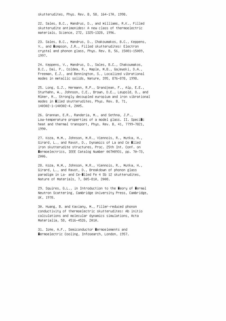
skutterudites, Phys. Rev. B, 58, 164–170, 1998.
22. Sales, B.C., Mandrus, D., and Williams, R.K., Filledskutterudite antimonides: A new class of thermoelectricmaterials, Science, 272, 1325–1328, 1996.
23. Sales, B.C., Mandrus, D., Chakoumakos, B.C., Keppens,V., and �ompson, J.R., Filled skutterudites: Electroncrystal and phonon glass, Phys. Rev. B, 56, 15081–15089,1997.
24. Keppens, V., Mandrus, D., Sales, B.C., Chakoumakos,B.C., Dai, P., Coldea, R., Maple, M.B., Gajewski, D.A.,Freeman, E.J., and Bennington, S., Localized vibrationalmodes in metallic solids, Nature, 395, 876–878, 1998.
25. Long, G.J., Hermann, R.P., Grandjean, F., Alp, E.E.,Sturhahn, W., Johnson, C.E., Brown, D.E., Leupold, O., andRü¤er, R., Strongly decoupled europium and iron vibrationalmodes in �lled skutterudites, Phys. Rev. B, 71,140302-1–140302-4, 2005.
26. Grannan, E.R., Randeria, M., and Sethna, J.P.,Low-temperature properties of a model glass. II. Speci�cheat and thermal transport, Phys. Rev. B, 41, 7799–7821,1990.
27. Koza, M.M., Johnson, M.R., Viennois, R., Mutka, H.,Girard, L., and Ravot, D., Dynamics of La and Ce �llediron skutterudite structures, Proc. 25th Int. Conf. on�ermoelectrics, IEEE Catalog Number 06TH8931, pp. 70–73,2006.
28. Koza, M.M., Johnson, M.R., Viennois, R., Mutka, H.,Girard, L., and Ravot, D., Breakdown of phonon glassparadigm in La- and Ce-�lled Fe 4 Sb 12 skutterudites,Nature of Materials, 7, 805–810, 2008.
29. Squires, G.L., in Introduction to the �eory of �ermalNeutron Scattering, Cambridge University Press, Cambridge,UK, 1978.
30. Huang, B. and Kaviany, M., Filler-reduced phononconductivity of thermoelectric skutterudites: Ab initiocalculations and molecular dynamics simulations, ActaMaterialia, 58, 4516–4526, 2010.
31. Io¤e, A.F., Semiconductor �ermoelements and�ermoelectric Cooling, Infosearch, London, 1957.
32. Rowe, D.M. and Bhangari, C.M., Modern �ermoelectrics,Holt, Rinehart and Winston, London, 1983.
33. Goldsmid, H.J., Electronic Refrigeration, Pion, London,1986.
34. Nolas, G.S., J. Sharp, and Goldsmid, H.J.,�ermoelectrics: Basic Principles and New MaterialsDevelopment, Springer-Verlag, Berlin, 2001.
35. Hicks, L.D. and Dresselhaus, M.S., E¤ect of quantumwell structures on the thermoelectric �gure of merit,Phys. Rev. B, 47, 12727–12731, 1993.
36. Hicks, L.D. and Dresselhaus, M.S., �ermoelectric �gureof merit of a one-dimensional conductor, Phys. Rev. B, 47,16631–16634, 1993.
37. Ravich, Y.I., E�mova, B.A., and Tamarchenko, V.I.,Scattering of current carriers and transport phenomena inlead chalcogenides, Phys. Stat. Solidi (b), 43, 453–469,1971.
38. Vashaee, D. and Shakouri, A., Improved thermoelectricpower factor in metal-based superlattices, Phys. Rev.Lett., 92, 106103-1–106103-4, 2004.
39. Harman, T.C., Taylor, P.J., Walsh, M.P., and Laforge,B.E., Quantum dot superlattice thermoelectric materialsand devices, Science, 297, 2229–2232, 2002.
40. Vineis, C.J., Harman, T.C., Calawa, S.D., Walsh, M.P.,Reeder, R.E., Singh, R., and Shakouri, A., Carrierconcentration and temperature dependence of the electronictransport properties of epitaxial PbTe and PbTe/PbSenanodot superlattices, Phys. Rev. B, 77, 235202-1–23520214,2008.
41. Koh, Y.K., Vineis, C.J., Calawa, S.D., Walsh, M.P., andCahill, D.G., Lattice thermal conductivity ofnanostructured thermoelectric materials based on PbTe,Appl. Phys. Lett., 94, 153101-1–153101-3, 2009.
42. Peierls, R.E., Quantum �eory of Solids, ClarendonPress, Oxford, 1955.
43. Berman, R., �ermal Conduction in Solids, ClarendonPress, Oxford, 1979.
44. Rayleigh, Lord, �eory of Sound (2nd edn.), Vol. 2,
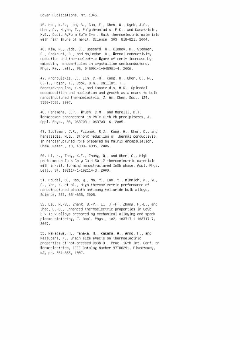
Dover Publications, NY, 1945.
45. Hsu, K.F., Loo, S., Guo, F., Chen, W., Dyck, J.S.,Uher, C., Hogan, T., Polychroniadis, E.K., and Kanatzidis,M.G., Cubic AgPb m SbTe 2+m : Bulk thermoelectric materialswith high �gure of merit, Science, 303, 818–821, 2004.
46. Kim, W., Zide, J., Gossard, A., Klenov, D., Stemmer,S., Shakouri, A., and Majumdar, A., �ermal conductivityreduction and thermoelectric �gure of merit increase byembedding nanoparticles in crystalline semiconductors,Phys. Rev. Lett., 96, 045901-1–045901-4, 2006.
47. Androulakis, J., Lin, C.-H., Kong, H., Uher, C., Wu,C.-I., Hogan, T., Cook, B.A., Caillat, T.,Paraskevopoulos, K.M., and Kanatzidis, M.G., Spinodaldecomposition and nucleation and growth as a means to bulknanostructured thermoelectric, J. Am. Chem. Soc., 129,9780–9788, 2007.
48. Heremans, J.P., �rush, C.M., and Morelli, D.T.�ermopower enhancement in PbTe with Pb precipitates, J.Appl. Phys., 98, 063703-1–063703- 6, 2005.
49. Sootsman, J.R., Pcionek, R.J., Kong, H., Uher, C., andKanatzidis, M.G., Strong reduction of thermal conductivityin nanostructured PbTe prepared by matrix encapsulation,Chem. Mater., 18, 4993– 4995, 2006.
50. Li, H., Tang, X.F., Zhang, Q., and Uher, C., Highperformance In x Ce y Co 4 Sb 12 thermoelectric materialswith in-situ forming nanostructured InSb phase, Appl. Phys.Lett., 94, 102114-1–102114-3, 2009.
51. Poudel, B., Hao, Q., Ma, Y., Lan, Y., Minnich, A., Yu,C., Yan, X. et al., High thermoelectric performance ofnanostructured bismuth antimony telluride bulk alloys,Science, 320, 634–638, 2008.
52. Liu, W.-S., Zhang, B.-P., Li, J.-F., Zhang, H.-L., andZhao, L.-D., Enhanced thermoelectric properties in CoSb3–x Te x alloys prepared by mechanical alloying and sparkplasma sintering, J. Appl. Phys., 102, 103717-1–103717-7,2007.
53. Nakagawa, H., Tanaka, H., Kasama, A., Anno, H., andMatsubara, K., Grain size e¤ects on thermoelectricproperties of hot-pressed CoSb 3 , Proc. 16th Int. Conf. on�ermoelectrics, IEEE Catalog Number 97TH8291, Piscataway,NJ, pp. 351–355, 1997.
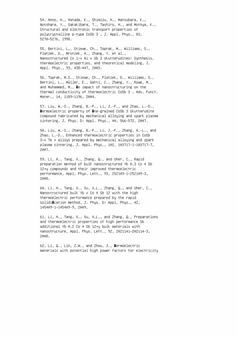
54. Anno, H., Hatada, K., Shimizu, H., Matsubara, K.,Notohara, Y., Sakakibara, T., Tashiro, H., and Motoya, K.,Structural and electronic transport properties ofpolycrystalline p-type CoSb 3 , J. Appl. Phys., 83,5270–5276, 1998.
55. Bertini, L., Stiewe, Ch., Toprak, M., Williams, S.,Platzek, D., Mrotzek, A., Zhang, Y. et al.,Nanostructured Co 1–x Ni x Sb 3 skutterudites: Synthesis,thermoelectric properties, and theoretical modeling, J.Appl. Phys., 93, 438–447, 2003.
56. Toprak, M.S., Stiewe, Ch., Platzek, D., Williams, S.,Bertini, L., Müller, E., Gatti, C., Zhang, Y., Rowe, M.,and Muhammed, M., �e impact of nanostructuring on thethermal conductivity of thermoelectric CoSb 3 , Adv. Funct.Mater., 14, 1189–1196, 2004.
57. Liu, W.-S., Zhang, B.-P., Li, J.-F., and Zhao, L.-D.,�ermoelectric property of �ne-grained CoSb 3 skutteruditecompound fabricated by mechanical alloying and spark plasmasintering, J. Phys. D: Appl. Phys., 40, 566–572, 2007.
58. Liu, W.-S., Zhang, B.-P., Li, J.-F., Zhang, H.-L., andZhao, L.-D., Enhanced thermoelectric properties in CoSb3–x Te x alloys prepared by mechanical alloying and sparkplasma sintering, J. Appl. Phys., 102, 103717-1–103717-7,2007.
59. Li, H., Tang, X., Zhang, Q., and Uher, C., Rapidpreparation method of bulk nanostructured Yb 0.3 Co 4 Sb12+y compounds and their improved thermoelectricperformance, Appl. Phys. Lett., 93, 252109-1–252109-3,2008.
60. Li, H., Tang, X., Su, X.L., Zhang, Q., and Uher, C.,Nanostructured bulk Yb x Co 4 Sb 12 with the highthermoelectric performance prepared by the rapidsolidi�cation method, J. Phys. D: Appl. Phys., 42,145409-1–145409-9, 2009.
61. Li, H., Tang, X., Su, X.L., and Zhang, Q., Preparationsand thermoelectric properties of high performance Sbadditional Yb 0.2 Co 4 Sb 12+y bulk materials withnanostructure, Appl. Phys. Lett., 92, 2021141–202114-3,2008.
62. Li, Q., Lin, Z.W., and Zhou, J., �ermoelectricmaterials with potential high power factors for electricity
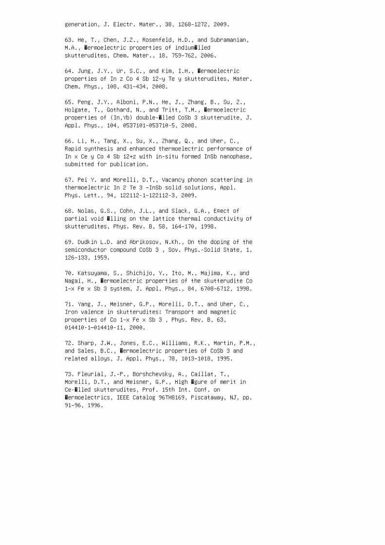
generation, J. Electr. Mater., 38, 1268–1272, 2009.
63. He, T., Chen, J.Z., Rosenfeld, H.D., and Subramanian,M.A., �ermoelectric properties of indium�lledskutterudites, Chem. Mater., 18, 759–762, 2006.
64. Jung, J.Y., Ur, S.C., and Kim, I.H., �ermoelectricproperties of In z Co 4 Sb 12–y Te y skutterudites, Mater.Chem. Phys., 108, 431–434, 2008.
65. Peng, J.Y., Alboni, P.N., He, J., Zhang, B., Su, Z.,Holgate, T., Gothard, N., and Tritt, T.M., �ermoelectricproperties of (In,Yb) double-�lled CoSb 3 skutterudite, J.Appl. Phys., 104, 0537101–053710-5, 2008.
66. Li, H., Tang, X., Su, X., Zhang, Q., and Uher, C.,Rapid synthesis and enhanced thermoelectric performance ofIn x Ce y Co 4 Sb 12+z with in-situ formed InSb nanophase,submitted for publication.
67. Pei Y. and Morelli, D.T., Vacancy phonon scattering inthermoelectric In 2 Te 3 –InSb solid solutions, Appl.Phys. Lett., 94, 122112-1–122112-3, 2009.
68. Nolas, G.S., Cohn, J.L., and Slack, G.A., E¤ect ofpartial void �lling on the lattice thermal conductivity ofskutterudites, Phys. Rev. B, 58, 164–170, 1998.
69. Dudkin L.D. and Abrikosov, N.Kh., On the doping of thesemiconductor compound CoSb 3 , Sov. Phys.-Solid State, 1,126–133, 1959.
70. Katsuyama, S., Shichijo, Y., Ito, M., Majima, K., andNagai, H., �ermoelectric properties of the skutterudite Co1–x Fe x Sb 3 system, J. Appl. Phys., 84, 6708–6712, 1998.
71. Yang, J., Meisner, G.P., Morelli, D.T., and Uher, C.,Iron valence in skutterudites: Transport and magneticproperties of Co 1–x Fe x Sb 3 , Phys. Rev. B, 63,014410-1—014410-11, 2000.
72. Sharp, J.W., Jones, E.C., Williams, R.K., Martin, P.M.,and Sales, B.C., �ermoelectric properties of CoSb 3 andrelated alloys, J. Appl. Phys., 78, 1013–1018, 1995.
73. Fleurial, J.-P., Borshchevsky, A., Caillat, T.,Morelli, D.T., and Meisner, G.P., High �gure of merit inCe-�lled skutterudites, Prof. 15th Int. Conf. on�ermoelectrics, IEEE Catalog 96TH8169, Piscataway, NJ, pp.91–96, 1996.
74. Sales, B.C., Mandrus, D., and Williams, R.K., Filledskutterudite antimonides: A new class of thermoelectricmaterials, Science, 272, 1325–1328, 1996.
75. Meisner, G.P., Morelli, D.T., Hu, S., Yang, J., andUher, C., Structure and lattice thermal conductivity offractionally �lled skutterudites: Solid solutions of fully�lled and un�lled end members, Phys. Rev. Lett., 80,3551–3554, 1998.
76. Uher, C., Li, C.-P., and Ballikaya, S.,Charge-compensated n-type skutterudites, J. Electron.Mater., 39, 2122–2126, 2010.
77. Dudkin L.D. and N. K. Abrikosov, N. Kh., E¤ect of Ni onthe properties of the semiconducting compound CoSb 3 , Zh.Neorg. Khim., 2, 212–221, 1957.
78. Anno, H., Matsubara, K., Notohara, Y., Sakakibara, T.,and Tashiro, H., E¤ect of doping on the transportproperties of CoSb 3 , J. Appl. Phys., 86, 3780–3786, 1999.
79. Dyck, J.S., Chen, W., Yang, J., Meisner, G.P., andUher, C., E¤ect of Ni on the transport and magneticproperties of Co 1–x Ni x Sb 3 , Phys. Rev. B, 65,115204-1–115204-9, 2002.
80. Zobrina B.N. and Dudkin, L.D., Investigation of thethermoelectric properties of CoSb 3 with Sn, Te, and Niimpurities, Sov. Phys.-Solid State, 1, 1668–1674, 1960.
81. Koyanagi, T., Tsubouchi, T., Ohtani, M., Kishimoto, K.,Anno, H., and Matsubara, K., �ermoelectric properties ofCo(M x Sb 1-x ) 3 (M = Ge, Sn, Pb) compounds, Proc. 15thInt. Conf. on �ermoelectrics, IEEE Catalog 96TH8169,Piscataway, NJ, pp. 107–111, 1996.
82. Y. Nagamoto, Y., Tanaka, K., and Koyanagi, T.,Transport properties of heavily doped n-type CoSb 3 ,Proc. 17th Int. Conf. on �ermoelectrics, IEEE CatalogNumber 98TH8365, Piscataway, NJ, pp. 302– 305, 1998.
83. Yang, J., Morelli, D.T., Meisner, G.P., Chen, W., Dyck,J.S., and Uher, C., E¤ect of Sn substituting for Sb on thelow-temperature transport properties of ytterbium-�lledskutterudites, Phys. Rev. B, 67, 165207-1–165207-6, 2003.
84. Li, X.Y., Chen, L.D., Fan, J.F., Zhang, W.B., Kawahara,T., and Hirai, T., �ermoelectric properties of Te-doped
CoSb 3 by spark plasma sintering, J. Appl. Phys., 98,083702-1–083702-6, 2005.
85. Wojciechowski, K.T., Tobola, J., and Leszczynski, J.,�ermoelectric properties and electronic structure of CoSb 3doped with Se and Te, J. Alloys and Comp., 361, 19–27,2003.
86. Liu, W.-S., Zhang, B.-P., Zhao, L.-D., and Li, J.-F.,Improvement of thermoelectric performance of CoSb 3–x Te xskutterudite compounds by additional substitution ofIVB-group elements for Sb, Chem. Mater., 20, 7526–7531,2008.
87. Su, X., Li, H., Wang, G., Chi, H., Zhou, X., Tang,X.F., Zhang, Q., and Uher, C., Structure and transportproperties of double-doped CoSb 2.75 Ge 0.25-x Te, (x =0.125-0.20) with in-situ nanostructure, Chem. Mater., 23,2948–2955, 2011.
88. Rogl, G., Grytsiv, A., Bauer, E., Rogl, P., andZehetbauer, M., �ermoelectric properties of novelskutterudites with didymium: DD y (Fe 1–x Co x ) 4 Sb 12and DD y (Fe 1–x Ni x ) 4 Sb 12 , Intermetallics, 18,57–64, 2010.
89. Salvador, J.R., Yang, J., Shi, X., Wang, H.,Wereszczak, A.A., Kong, H., and Uher, C., Transport andmechanical properties of Yb-�lled skutterudites, Philos.Mag., 89, 1517–1534, 2009.
90. Zhang, L., Rogl, G., Grytsiv, A., Ruchegger, S.,Koppensteiner, J., Spieckermann, F., Kabelka, H. et al.,Mechanical properties of �lled antimonide skutterudites,Mater. Sci. Eng. B, 170, 26–31, 2010.
91. Uher, C., Skutterudites: Promising power conversionthermoelectric. In Proceedings of the 22nd InternationalConference on �ermoelectrics, pp. 42–47. IEEE CatalogNumber 03TH8726, Piscataway, NJ, 2003.
11 Chapter 11 - Silicide Thermoelectrics:State of the Art and Prospects
1. Nikitin E.N. Zhurnal Tekhnicheskoj Fiziki 28, 23, 1958(in Russian).
2. Nikitin E.N., Bazanov V.G., Tarasov V.I. Sov. Phys.Solid State 3(12), 2650–2651, 1961.
3. Zaitsev V.K., Fedorov M.I., Gurieva E.A., Eremin I.S.,Konstantinov P.P., Samunin A.Yu., Vedernikov M.V. Phys.Rev. B 74, 045207, 2006.
4. Maex K. van Rossum M. (Ed.), Properties of MetalSilicides, INSPEC, London, 1995. See articles by M.Ostling and C. Zaring (pp. 15 and 31).
5. Samsonov G.V., Vinetskii I.M. Handbook of RefractoryCompounds, Plenum Press, New York, 1980.
6. Karpinskij O.G., Evseev V.A. Izv. AN SSSR (Neorg.Mater.) 5, 525, 1969 (in Russian).
7. Wandji R., Dusausoy Y., Protas J., Roques B. C.R. Acad.Sci. C. 267, 1587, 1968.
8. Poutcharovsky D.J., Parthe E. Acta Crystallogr. B 30,2692, 1974.
9. Gottlieb U., Lambert-Andron B., Nava F., A¤ronte M.,Laborde O., Rouault A., Madar R. J. Appl. Phys. 78, 3902,1995.
10. Fedorov M.I., Germanovich O.S., Zaitsev V.K.�ermoelectrics and �eir Applications, Io¤ePhysicalTechnical Institute, St. Petersburg, p. 269, 2008(in Russian).
11. Kuramitsu M., Yoshio M., Takeda M., Ohsugi I.J. 23rdInternational Conference on �ermoelectrics, Adelaide,Australia, Proceedings ICT’2004. IEEE, #125, 2005.
12. Ishida Y., Kayamura K., Takeda M., Ohsugi I.J. XXVInternational Conference on �ermoelectrics, Vienna,Austria, Proceedings ICT’2006, IEEE, 566, 2006.
13. Zaitsev V.K., Andreev A.A., Ivanov Yu.V., Fedorov M.I.�ermoelectrics and �eir Applications, Io¤ePhysical-Technical Institute, St. Petersburg, 226, 2008(in Russian).
14. Solomkin F.Yu., Zaitsev V.K., Kartenko N.F., KolosovaA.S. �ermoelectrics and �eir Applications, Io¤ePhysical-Technical Institute, St. Petersburg, 257, 2008 (inRussian).
15. Voronov B.K., Dudkin L.D., Trusova N.N. Khimicheskayasvyaz v poluprovodnikah, Minsk, “Nauka i Tekhnika,” 291,1969 (in Russian).
16. Zaitsev V.K. CRC Handbook of �ermoelectrics, ed. RoweD.M., CRC Press, New York, p. 299, 1995.
17. Hesse J.Z. Angew, Phys., 28, 133, 1969.
18. Birkholz U., Gross E., Stoehrer U. Polycrystalline, inCRC Handbook of �ermoelectrics, ed. by Rowe D.M., CRCPress, New York, p. 287, 1995.
19. Chen H.Y., Zhao X.B., Stiewe C., Platzek D., Mueller E.J. Alloys Comp., 433, 338, 2007.
20. Arita Y., Mitsuda S., Nishi Y., Matsui T., Nagasaki T.J. Nucl. Mater. 294, 202, 2001.
21. Ivanenko L., Filonov A., Shaposhnikov V., KrivosheevA., Behr G., Souptel D., Schumann J. et al. Twenty-SecondInternational Conference on �ermoelectrics, La GrandeMotte, France, Proceedings of ICT’03, IEEE, p. 157, 2003.
22. Simkin B.A., Hayashi Y., Inui H. Intermetallics 13,1225, 2005.
23. Sakamaki Y., Kuwabara K., Jiajun G., Inui H., YamaguchiM., Yamamoto A., Obara H. Mater. Sci. Forum 426–432, 1777,2003.
24. Gu J.-J., Oh M.-W., Inui H., Zhang D. Phys. Rev. B 71,113201, 2005.
25. Sugihara, S., Morikawa, K., Igarashi, Y., Nishiyama, K.XXV International Conference on �ermoelectrics, Vienna,Austria, Proceedings ICT’06, IEEE, p. 711, 2006.
26. Fedorov M.I., Zaitsev V.K., Vedernikov M.V. XXVInternational Conference on �ermoelectrics, Vienna,Austria, Proceedings ICT’06, IEEE, p. 111, 2006.
27. Zaitsev Z.V.K., Fedorov M.I., Eremin I.S., GurievaE.A., �ermoelectrics Handbook: Macro to Nano, CRC Press,
New York, Chapter 29, 2006.
28. Tani J., Kido H. Jap. J. Appl. Phys. 46, 3309, 2007.
29. Tani J., Kido H. J. Alloys Compounds 466, 335, 2008.
30. Zhang Q., He J., Zhao H.B., Zhang S.N., Zhu T.J., YinH., Tritt T.M. J. Phys. D 41, 185103, 2008.
31. Labotz R.J., Mason D.R. J. Electrochem. Soc. 110, 120,1963.
32. Zaitsev V.K. �ermoelectric Properties and �ermalConductivity of Some Solid Solution Based on MagnesiumStannide, PhD thesis, Leningrad, 1969.
33. Tani J., Kido H. Intermetallics 15, 1202, 2007.
34. Tani J.-I., Kido H. Physica B 364, 218, 2005.
35. Mars K., Ihou-Mouko H., Pont G., Tobola J., Scherrer H.J. Electron. Mater. 38, 1360, 2009.
36. Akasaka M., Iida T., Matsumoto A., Yamanaka K.,Takanashi Y., Imai T., Hamada N. J. Appl. Phys. 104,013703, 2008.
37. Labotz R.J., Mason D.R., O’Kane D.F. J. Electrochem.Soc. 110, 127, 1963.
38. Akasaka M., Iida T., Nishio K., Takanashi Y. �in SolidFilms 515, 8237, 2007.
39. Isoda Y., Shioda N., Fujiu H., Imai Y., Shinohara Y.23rd International Conference on �ermoelectrics, Adelaide,Australia, Proceedings ICT’2004, #124.pdf, 2004.
40. Pshenay-Severin D.A., Fedorov M.I. Phys. Sol. St. 49,1633, 2007.
41. Isoda Y., Nagai T., Fujiu H., Imai Y., Shinohara Y.XXVI International Conference on �ermoelectrics, Jeju,Korea, Proceedings ICT’07, IEEE, 251, 2007.
42. Isoda Y. , Nagai T., Fuziu H., Imai Y., Shinohara Y.XXV International Conference on �ermoelectrics, Vienna,Austria, Proceedings ICT’06, IEEE, p. 406, 2006.
43. Zhang Q., He J., Zhu T.J., Zhang S.N., Zhao X.B., TrittT.M. Appl. Phys. Lett. 93, 102109, 2008.
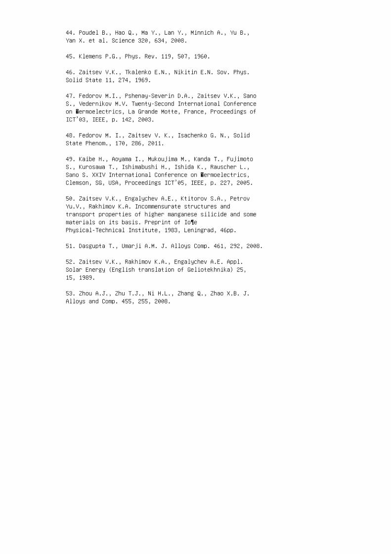
44. Poudel B., Hao Q., Ma Y., Lan Y., Minnich A., Yu B.,Yan X. et al. Science 320, 634, 2008.
45. Klemens P.G., Phys. Rev. 119, 507, 1960.
46. Zaitsev V.K., Tkalenko E.N., Nikitin E.N. Sov. Phys.Solid State 11, 274, 1969.
47. Fedorov M.I., Pshenay-Severin D.A., Zaitsev V.K., SanoS., Vedernikov M.V. Twenty-Second International Conferenceon �ermoelectrics, La Grande Motte, France, Proceedings ofICT’03, IEEE, p. 142, 2003.
48. Fedorov M. I., Zaitsev V. K., Isachenko G. N., SolidState Phenom., 170, 286, 2011.
49. Kaibe H., Aoyama I., Mukoujima M., Kanda T., FujimotoS., Kurosawa T., Ishimabushi H., Ishida K., Rauscher L.,Sano S. XXIV International Conference on �ermoelectrics,Clemson, SG, USA, Proceedings ICT’05, IEEE, p. 227, 2005.
50. Zaitsev V.K., Engalychev A.E., Ktitorov S.A., PetrovYu.V., Rakhimov K.A. Incommensurate structures andtransport properties of higher manganese silicide and somematerials on its basis. Preprint of Io¶ePhysical-Technical Institute, 1983, Leningrad, 46pp.
51. Dasgupta T., Umarji A.M. J. Alloys Comp. 461, 292, 2008.
52. Zaitsev V.K., Rakhimov K.A., Engalychev A.E. Appl.Solar Energy (English translation of Geliotekhnika) 25,15, 1989.
53. Zhou A.J., Zhu T.J., Ni H.L., Zhang Q., Zhao X.B. J.Alloys and Comp. 455, 255, 2008.
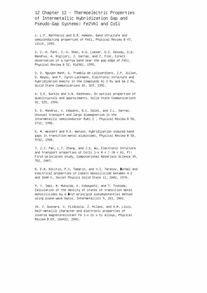
12 Chapter 12 - Thermoelectric Propertiesof Intermetallic Hybridization Gap andPseudo-Gap Systems: Fe2VAl and CoSi
1. L.F. Mattheiss and D.R. Hamann, Band structure andsemiconducting properties of FeSi, Physical Review B 47,13114, 1993.
2. C.-H. Park, Z.-X. Shen, A.G. Loeser, D.S. Dessau, D.G.Mandrus, A. Migliori, J. Sarrao, and Z. Fisk, Directobservation of a narrow band near the gap edge of FeSi,Physical Review B 52, R16981, 1995.
3. D. Nguyen Manh, G. Trambly de Laissardiere, J.P. Julien,D. Mayou, and F. Cyrot-Lackmann, Electronic structure andhybridization e¤ects in the compounds Al 2 Ru and Ga 2 Ru,Solid State Communications 82, 329, 1992.
4. S.E. Burkov and S.N. Rashkeev, On optical properties ofquasicrystals and approximants, Solid State Communications92, 525, 1994.
5. D. Mandrus, V. Keppens, B.C. Sales, and J.L. Sarrao,Unusual transport and large diamagnetism in theintermetallic semiconductor RuAl 2 , Physical Review B 58,3712, 1998.
6. M. Weinert and R.E. Watson, Hybridization-induced bandgaps in transition-metal aluminides, Physical Review B 58,9732, 1998.
7. Z.J. Pan, L.T. Zhang, and J.S. Wu, Electronic Structureand transport properties of Co(Si 1−x M x ) (M = Al, P):First-principles study, Computational Materials Science 39,752, 2007.
8. E.N. Nikitin, P.V. Tamarin, and V.I. Tarasov, �ermal andelectrical properties of cobalt monosilicide between 4.2and 1600 K, Soviet Physics Solid State 11, 2002, 1970.
9. Y. Imai, M. Mukaida, K. Kobayashi, and T. Tsunoda,Calculation of the density of states of transition metalmonosilicides by a �rst-principle pseudopotential methodusing plane-wave basis, Intermetallics 9, 261, 2001.
10. J. Guevara, V. Vildosola, J. Milano, and A.M. Llois,Half-metallic character and electronic properties ofinverse magnetoresistant Fe 1−x Co x Si alloys, PhysicalReview B 69, 184422, 2002.
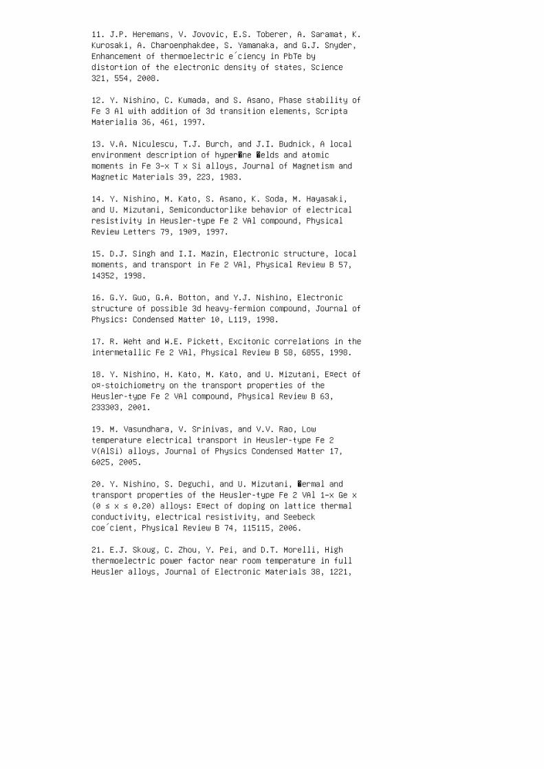
11. J.P. Heremans, V. Jovovic, E.S. Toberer, A. Saramat, K.Kurosaki, A. Charoenphakdee, S. Yamanaka, and G.J. Snyder,Enhancement of thermoelectric e´ciency in PbTe bydistortion of the electronic density of states, Science321, 554, 2008.
12. Y. Nishino, C. Kumada, and S. Asano, Phase stability ofFe 3 Al with addition of 3d transition elements, ScriptaMaterialia 36, 461, 1997.
13. V.A. Niculescu, T.J. Burch, and J.I. Budnick, A localenvironment description of hyper�ne �elds and atomicmoments in Fe 3−x T x Si alloys, Journal of Magnetism andMagnetic Materials 39, 223, 1983.
14. Y. Nishino, M. Kato, S. Asano, K. Soda, M. Hayasaki,and U. Mizutani, Semiconductorlike behavior of electricalresistivity in Heusler-type Fe 2 VAl compound, PhysicalReview Letters 79, 1909, 1997.
15. D.J. Singh and I.I. Mazin, Electronic structure, localmoments, and transport in Fe 2 VAl, Physical Review B 57,14352, 1998.
16. G.Y. Guo, G.A. Botton, and Y.J. Nishino, Electronicstructure of possible 3d heavy-fermion compound, Journal ofPhysics: Condensed Matter 10, L119, 1998.
17. R. Weht and W.E. Pickett, Excitonic correlations in theintermetallic Fe 2 VAl, Physical Review B 58, 6855, 1998.
18. Y. Nishino, H. Kato, M. Kato, and U. Mizutani, E¤ect ofo¤-stoichiometry on the transport properties of theHeusler-type Fe 2 VAl compound, Physical Review B 63,233303, 2001.
19. M. Vasundhara, V. Srinivas, and V.V. Rao, Lowtemperature electrical transport in Heusler-type Fe 2V(AlSi) alloys, Journal of Physics Condensed Matter 17,6025, 2005.
20. Y. Nishino, S. Deguchi, and U. Mizutani, �ermal andtransport properties of the Heusler-type Fe 2 VAl 1−x Ge x(0 ≤ x ≤ 0.20) alloys: E¤ect of doping on lattice thermalconductivity, electrical resistivity, and Seebeckcoe´cient, Physical Review B 74, 115115, 2006.
21. E.J. Skoug, C. Zhou, Y. Pei, and D.T. Morelli, Highthermoelectric power factor near room temperature in fullHeusler alloys, Journal of Electronic Materials 38, 1221,
2009.
22. C.S. Lue, Y.K. Kuo, S.N. Horng, S.Y. Peng, and C.Chent, Structural, thermal, and electronic properties of Fe2 VSi 1−x Al x , Physical Review B 71, 064202, 2005.
23. C.S. Lue, C.F. Chen, J.Y. Lin, Y.T. Yu, and Y.K. Kuo,�ermoelectric properties of quaternary Heusler alloys Fe 2VAl 1−x Si x , Physical Review B 75, 064204, 2007.
24. C.S. Lue and Y.K. Kuo, �ermoelectric properties of thesemimetallic Heusler compounds Fe 2−x V 1+x M (M = Al,Ga), Physical Review B 66, 085121, 2002.
25. G. Ghosh, G.V. Narasimha Roa, V.S. Sastry, A. Bharathi,Y. Hariharan, and T.S. Radhakrishnan, X-ray powderdi¤raction data of CoSi, Powder Di¶raction 12, 252, 1997.
26. W.L. Ren, C.C. Li, L.T. Zhang, K. Ito, and J.S. Wu,E¤ects of Ge and B substitution on thermoelectricproperties of CoSi, Journal of Alloys and Compounds 392,50, 2005.
27. C.S. Lue, Y.K. Kuo, C.L. Huang, and W.J. Lai,Hole-doping e¤ect on the thermoelectric properties andelectronic structure of CoSi, Physical Review B 69, 125111,2004.
28. S. Asanabe, D. Shinoda, and Y. Sasaki, Semimetallicproperties of Co 1−x Fe x Si solid solutions, PhysicalReview 134, A774, 1964.
29. M.I. Fedorov and V.K. Zaitsev, Semimetals as materialsfor thermoelectric generators, in CRC Handbook of�ermoelectrics, ed. D.M. Rowe (CRC Press, Boca Raton,1995), p. 321.
30. Y.K. Kuo, K.M. Sivakumar, S.J. Huang, and C.S. Lue,�ermoelectric properties of CoSi 1−x Ge x alloys, Journalof Applied Physics 98, 123510, 2005.
31. E. Skoug, C. Zhou, Y. Pei, and D.T. Morelli, Highthermoelectric power factor in alloys based on CoSi,Applied Physics Letters 94, 022115, 2009.
32. F. Wald and S.J. Michalik, �e ternary systemcobalt-germanium-silicon, Journal of the Less-CommonMetals 24, 277, 1971.
33. C.C. Li, W.L. Ren, L.T. Zhang, K. Ito, and J.W. Su,

E¤ects of Al doping on the thermoelectric performance ofCoSi single crystal, Journal of Applied Physics 98, 063706,2005.
13 Chapter 13 - Novel Power Factor ofSi–Ge System
1. Vining, C. B. 1955. CRC Handbook of �ermoelectrics,edited by D. M. Rowe, pp. 329–337. Boca Raton: CRC Press.
2. Okamoto, Y., Uchino, H., Kawahara, T., and Morimoto, J.1999. Anomalous large thermoelectric power of the Si andAu doped Ge superlattice thin �lm. Jpn. J. Appl. Phys. 38:L945–L947.
3. Uchino, H., Okamoto, Y., Kawahara, T., and Morimoto, J.2000. �e study of the origin of the anomalous largethermoelectric power of the Si and Au doped Ge superlatticethin �lm. Jpn. J. Appl. Phys. 39: 1675–1677.
4. Kawahara, T., Lee, S. M., Okamoto, Y., Morimoto, J.,Sasaki, K., and Hata, T. 2002. Anomalous largethermoelectric power on heavily B-doped SiGe thin �lms.Jpn. J. Appl. Phys. 41: L949–L951.
5. Yamamoto, A., Takimoto, M., Ohta, T., Whitlow, L., Miki,K., Sakamoto, K., and Kamisako, K. 1998. Two dimensionalquantum net of heavily doped porous silicon. Proc. of 17thInt. Conf. �ermoelectrics, Nagoya, pp. 198–201.
6. Yamamoto, A., Takazawa, H., and Ohta, T. 1999.�ermoelectric transport properties of porous siliconnanostructure. Proc. of 18th Int. Conf. �ermoelectrics,Baltimore, pp. 428–431.
7. Kodato, S. 1985. Si-Gealloy �lm with very highelectrical conductivity and thermoelectric power.J. Non-Cryst. Sol. 77&78: 893–896.
8. Lee, S. M., Okamoto, Y., Kawahara, T., and Morimoto, J.2002. �e fabrication and thermoelectric properties ofamorphous Si–Ge–Au bulk samples. Mat. Res. Soc. Proc. 691:215–220.
9. Abe, M, Takiguchi, H., Okamoto, Y., Miyazaki, H., andMorimoto, J. 2009. Mechanical fabrication of Si–Ge–B bulksamples with superior thermoelectric power. Mat. Res. Soc.Proc. 1145: 1145-MM04-07.
10. Lee, S. M., Okamoto, Y., Kawahara, T., and Morimoto,J., 2002. Annealing temperature dependence of theamorphous structure of amorphous Si–Ge–Au thin �lms. Jpn.J. Appl. Phys. 41: 5336–5337.
11. Okamoto, Y., Miyata, A., Sato, Y., Takiguchi, H.,Kawahara, T., and Morimoto, J. 2003. �e measurement ofannealing cycle e¤ects of Si–Ge–Au amorphous thin �lm withanomalously large thermoelectric power by usingphotoacoustic spectroscopy. Jpn. J. Appl. Phys. 42:3048–3051.
12. Takiguchi, H., Matoba, A., Sasaki, K., Okamoto, Y.,Miyazaki, H., and Morimoto, J. 2000. Structural propertiesof heavily B-doped SiGe thin �lms for high thermoelectricpower. Mater. Trans. 51: 878–881.
13. Takiguchi, H., Fukui, K., and Okamoto, Y. 2010.Annealing temperature dependence of crystallization processof SiGeAu thin �lm. Jpn. J. Appl. Phys. 49: 115602–115607.
14. Takiguchi, H., Aono, M., and Okamoto, Y. 2011.Nano-structural and thermoelectric properties of SiGeAuthin �lms. Jpn. J. Appl. Phys. 50: 041301-1–041301-5.
15. Sasaki, K., Nabetani, Y., Miyashita, H., and Hata, T.2000. Heteroepitaxial growth of SiGe �lms and heavy Bdoping by ion-beam sputtering. �in Solid Films 369:171–174. 900 10 8 6 4 2 0 C r y s t a l l i t e d i a m e te r ( n m ) 950 1000 Annealing temperature, T (K)
FIGURE 13.33 �e grain size of SiGeB thin �lm estimated from(1 1 1) plane peak of XRD measurement as a
function of annealing temperature. (Adapted from Takiguchi,H. et al., 2000. Mater. Trans. 51: 878–881.)
16. Okamoto, Y., Saeki, J., Ohstuki, T., and Takiguchi, H.2010. Structural e¤ects on thermal conductivity of SiGeAusuperlattice thin �lms. Jpn. J. Appl. Phys. 49:85801–85805.
17. Abe, M. 2009. Mechanical fabrication of Si–Ge bulksamples with superior thermoelectric power. Master’sthesis, National Defense Academy, Kanagawa in Japanese.
18. Lee, S. M., Okamoto, Y., Kawahara, T., and Morimoto, J.2002. E¤ects of substrate temperature on thermoelectricproperties of amorphous Si/Ge thin �lms. Proc. of 20th Int.Conf. �ermoelectrics, Beijing, pp. 348–351.
19. Lee, S. M., Okamoto, Y., Kawahara, T., and Morimoto, J.2003. �e study for the mechanism on the noblethermoelectric properties of the amorphous Si-Ge-Au thin�lms. Proc. of 21th Int. Conf. �ermoelectrics, Long Beach,
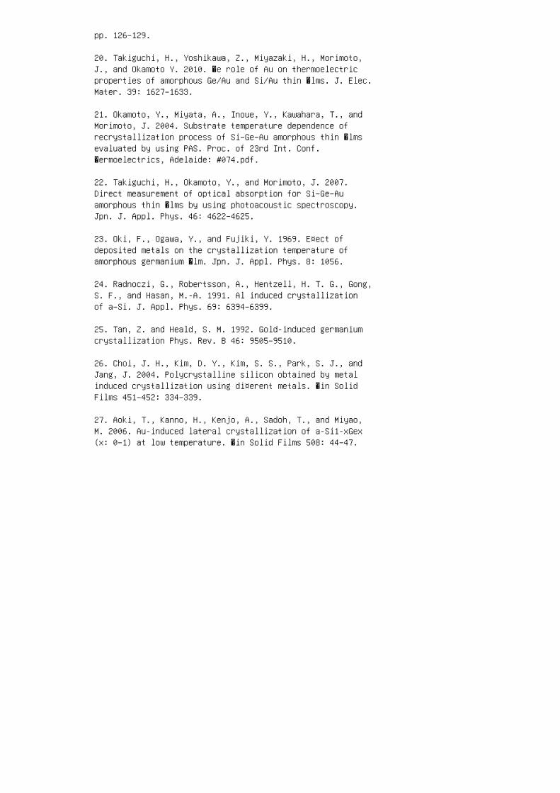
pp. 126–129.
20. Takiguchi, H., Yoshikawa, Z., Miyazaki, H., Morimoto,J., and Okamoto Y. 2010. �e role of Au on thermoelectricproperties of amorphous Ge/Au and Si/Au thin �lms. J. Elec.Mater. 39: 1627–1633.
21. Okamoto, Y., Miyata, A., Inoue, Y., Kawahara, T., andMorimoto, J. 2004. Substrate temperature dependence ofrecrystallization process of Si–Ge–Au amorphous thin �lmsevaluated by using PAS. Proc. of 23rd Int. Conf.�ermoelectrics, Adelaide: #074.pdf.
22. Takiguchi, H., Okamoto, Y., and Morimoto, J. 2007.Direct measurement of optical absorption for Si–Ge–Auamorphous thin �lms by using photoacoustic spectroscopy.Jpn. J. Appl. Phys. 46: 4622–4625.
23. Oki, F., Ogawa, Y., and Fujiki, Y. 1969. E¤ect ofdeposited metals on the crystallization temperature ofamorphous germanium �lm. Jpn. J. Appl. Phys. 8: 1056.
24. Radnoczi, G., Robertsson, A., Hentzell, H. T. G., Gong,S. F., and Hasan, M.-A. 1991. Al induced crystallizationof a–Si. J. Appl. Phys. 69: 6394–6399.
25. Tan, Z. and Heald, S. M. 1992. Gold-induced germaniumcrystallization Phys. Rev. B 46: 9505–9510.
26. Choi, J. H., Kim, D. Y., Kim, S. S., Park, S. J., andJang, J. 2004. Polycrystalline silicon obtained by metalinduced crystallization using di¤erent metals. �in SolidFilms 451–452: 334–339.
27. Aoki, T., Kanno, H., Kenjo, A., Sadoh, T., and Miyao,M. 2006. Au-induced lateral crystallization of a-Si1-xGex(x: 0–1) at low temperature. �in Solid Films 508: 44–47.
14 Chapter 14 - Boride Thermoelectrics:High-Temperature Thermoelectric Materials
1. Slack G.A., Oliver D.W., and Horn F.H., Phys. Rev. B, 4,1714–1720, 1971.
2. Cahill D.G., Fischer H.E., Watson S.K., Pohl R.O., andSlack G.A., Phys. Rev. B, 40, 3254–3260, 1989.
3. Mori T., Physica B, 383, 120–121, 2006.
4. Mori T., Martin J., and Nolas G., J. Appl. Phys., 102,073510, 2007.
5. Mori T., Higher borides, in Gschneidner Jr. K.A., BunzliJ.C., Pecharsky V., editors. Handbook on the Physics andChemistry of Rare Earths, Vol. 38, Elsevier, Amsterdam,North-Holland, 2008, 105–173.
6. Mori T. and Nishimura T., J. Solid State Chem., 179,2908, 2006.
7. Mori T., Nishimura T., Yamaura K., andTakayama-Muromachi E., J. Appl. Phys., 101, 093714, 2007.
8. Emin D., J. Solid State Chem., 177, 1619, 2004.
9. Ghamaty S., Bass J.C., and Elsner N.B., in, Rowe D.M.,editor. �ermoelectrics Handbook, Micro to Nano, BocaRaton, CRC Press, 2006, 57.
10. Longuet H.C. and Roberts M. DeV., Proc. Roy. Soc. A,230, 110, 1955.
11. Samsonov G.V., Makarenko G.N., and Tsebulya G. G., Izv.Akad. Nauk SSSR, Otd. Tekhn. Nauk, 4, 1960.
12. Wood C. and Emin D., Phys. Rev. B, 29, 4582–4587, 1984.
13. Aselage T.L., Emin D., McCready S.S., and Duncan R.V.,Phys. Rev. Lett., 81, 2316–2319, 1998.
14. Aselage T.L. and Emin D., in, Kanatzidis, M.G., editor.Chemistry, Physics and Materials Science of �ermoelectricMaterials, Beyond Bismuth Telluride. Dordrecht, KluwerAcademic, 2003, 55.
15. Aselage T.L. and Emin D., in Rowe D.M., editor.�ermoelectrics Handbook, Boca Raton, CRC Press, 2002, 31.
16. Emin D., Phys. Rev. B, 38, 6041, 1988.
17. Werheit, H., Rotter, H.W., Meyer, F.D., Hillebrecht,H., Shalamberidze, S.O., Abzianidze, T.G., and Esadze,G.G., J. Solid State Chem., 177, 569–574, 2004.
18. Emin D., Phys. Today, 40, 55, 1987.
19. Werheit, H., J. Phys., Condens. Matter, 18,10655–10662, 2006.
20. Cai K.F., Nan C.W., and Min X.M., Mater. Res. Soc.Symp. Proc., 545, 131, 1999.
21. Goto T., Kinzoku (in Japanese), 68, 1086, 1998.
22. Liu C.H., Mater. Lett., 49, 308–312, 2001.
23. Lunca-Popa P., Brand J.I., Balaz S., Rosa L.G., BoagN.M., Bai M., Robertson B.W., and Dowben P.A., J. Phys. D,38, 1248, 2005.
24. Slack G.A., Rosolowski J.H., Hejna C., Garbauskas M.,and Kasper J.S., Proc. 9th Int. Symp. Boron, Borides andRelated Compounds, Duisberg, 1987, 132.
25. Golikova O.A., Amandzhanov N., Kazanin M.M., KlimashinG.M., and Kutasov V.V., Phys. Stat. Sol., 121, 579, 1990.
26. Slack G.A., Hejna C.I., Garbauskas M.F., and KasperJ.S., J. Solid State Chem., 76, 52, 1988.
27. Werheit H., Schmechel R., Kue¤el V., and Lundström T.,J. Alloys. Compd., 262–263, 372, 1997.
28. Nakayama T., Shimizu J., and Kimura K., J. Solid StateChem., 154, 13, 2000.
29. Paderno Yu.B., Poroshk. Metallurgija, 11, 70–73, 1969;Paderno Yu.B., Electron. Technol., 3, 175, 1970.
30. Etourneau J., J. Solid State Chem., 2, 332–342, 1970.
31. Avetisyan A.O., Goryachev Yu.M., Kovenskaya B.A., andShvartsman E.I., Izv. Akad. Nauk SSSR Neorg. Mater., 15,663–666, 1979.
32. Yagasaki K., Notsu S., Shimoji Y., Nakama T., Kaji R.,Yokoo T., Akimitsu J., Hedo M., and Uwatoko Y., Physica B,329–333, 1259–1260, 2003.
33. Takeda M., Fukuda T., Domingo F., and Miura T., J.Solid State Chem., 177, 471–475, 2004.
34. Takeda M., Domingo F., Miura T., and Fukuda T., Mater.Res. Soc. Symp. Proc., 691, 209–214, 2002.
35. Golikova O.A., Phys. Stat. Sol. A, 101, 277, 1987.
36. Richards S.M. and Kasper J.S., Acta Cryst. B, 25, 237,1969.
37. Higashi I., Kobayashi K., Tanaka T., and Ishizawa Y.,J. Solid State Chem., 133, 16, 1997.
38. Tanaka T., Kamiya K., Numazawa T., Sato A., andTakenouchi S., Z. Kristallogr., 221, 472, 2006.
39. Mori T. and Tanaka T., J. Solid State Chem., 179,2889–2894, 2006.
40. Mott N.F., J. Non-Cryst. Solids, 1, 1, 1968.
41. Efros A.L. and Shklovskii B.I., in, Efros A.L., andPollak M., editor. Electron–Electron Interactions inDisordered Systems, North-Holland, Amsterdam, 1985,409–482.
42. Berthebaud D., Nishimura T., and Mori T., J. Mater.Res., 25, 665–669, 2010.
43. Berthebaud D., Nishimura T., and Mori T., J. Electron.Mat., 40, 682–686, 2011.
44. Mori T., Burkhardt U., Schnelle W., and Grin Y., Originof the n-type behavior in rare earth boron carbonitrides,to be submitted.
45. Prytuliak A. and Mori T., J. Electron. Mat., 40,920–925, 2011.
46. Prytuliak A. and Mori T., Vanadium seeding e¤ect on YB22 C 2 N, to be submitted.
47. Higashi I., Tanaka T., Kobayashi K., Ishizawa Y., andTakami M., J. Solid State Chem., 133, 11, 1997.
48. Mori T. and Tanaka T., J. Phys. Soc. Jpn., 68,2033–2039, 1999.
49. Mori T., J. Appl. Phys., 97, 093703, 2005.
50. Mori T., Berthebaud D., Nishimura T., Nomura A.,Shishido T., and Nakajima K., Dalton Trans., 39,1027–1030, 2010.
51. Poudel B., Hao Q., Ma Y., Lan Y., Minnich A., Yu B. YanX. et al., Science, 320, 634, 2008.
52. Slack G.A., in Seitz F., Turnbull D., and Ehrenreich H.editors. Semiconductors and Semimetals, Vol. 34, ed.,Academic Press, New York, 1979, 1.
55. Nolas G.S., Slack G.A., Morelli D.T., Tritt T.M., andEhrlich A.C., J. Appl. Phys., 79, 4002, 1996.
56. Mori T., J. Soc. Inorg. Mater. Jpn., 17, 428, 2010.
15 Chapter 15 - Polymer ThermoelectricMaterials
1. R. Venkatasubramanian, E. Siivola, T. Colpitts, B.O’Quinn, �in-�lm thermoelectric devices with highroom-temperature �gures of merit, Nature, 413, 597, 2001.
2. K. Tanaka, K. Akagi, Evolution of conductive polymers,In Dr. Hideki Shirakawa and Conductive Polymers, editors,K. Akagi, K. Tanaka, Tokyo, Kagaku-Dojin, Publishing Co.,Inc., p. 53, 2002.
3. Y. Shinohara et al., Power evaluation of PbTe withcontinuous carrier concentration gradient, MaterialsScience Forum, 492–493, 141, 2005.
4. Y. Shinohara et al., A new challenge of polymerthermoelectric materials as ecomaterials, MaterialsScience Forum, 539–543, 2329, 2007.
5. N. Toshima, H. Yan, T. Ohta, Electrically conductivepolyaniline �lms as organic thermoelectric materials,Proc. 19th Int. Conf. �ermoelectrics, Cardi¤, UnitedKingdom, p. 214, 2000.
6. H.Yan, T. Ohta, N. Toshima, Stretched polyaniline �lmsdoped by (±)-10-camphorsulfonic acid: Anisotropy andimprovement of thermoelectric properties, Macromol. Mater.Eng., 286, 139, 2001.
7. N. Toshima, H. Yan, M. Kajita, �ermoelectric propertiesof spin-coated polyaniline �lms, Proc. 21st Int. Conf.�ermoelectrics, Longbeach, p. 147, 2002.
8. H. Yan, T. Isida, N. Toshima, �ermoelectric propertiesof electrically conductive polypyrrole �lm, Proc. 20thInt. Conf. �ermoelectrics, Beijing, p. 310, 2001.
9. N. Toshima, Conductive polymers as a candidate oforganic thermoelectric materials, Material Stage, 10(1),42, 2010.
10. N. Toshima, Organic-inorganic hybrid, In Handbook of�ermoelectric Energy Conversions, editor, T. Kajikawa,Tokyo, NTS, p. 320, 2009.
11. D. Moses, A. Denenstein, J. Chen, A. J. Heeger, P.McAndrew, T. Woerner, A. G. MacDiarmid, Y. W. Park, E¤ectof nonuniform doping on electrical transport in trans-(CH)x : Studies of the semiconductor-metal transition,
Physical Review B, 25(12), 7652, 1982.
12. Y. W. Park, Y. S. Lee, C. Park, L. W. Shacklette, R. H.Baughman, �ermopower and conductivity of metallicpolyaniline, Solid State Communications, 63(11), 1063,1987.
16 Chapter 16 - ThermomechanicalProperties of Thermoelectric Materials
Ainsworth, J.H. and Herron, R.H., �ermal damage resistanceof refractories, Am. Ceram. Soc. Bull., 53:533–538, 1974.
Andersson, T. and Rowcli¤e, D.J., �ermal cycling ofindented ceramic materials, J. Eur. Ceramic Soc.,18:2065–2071, 1998.
Ashizuka, M., Easler, T.E. and Bradt, R.C., Statisticalstudy of thermal shock damage of a borosilicate glass, J.Am. Ceram. Soc., 66:542–550, 1983.
ASTM C 1161-02c, Standard test method for ¡exural strengthof advanced ceramics at ambient temperatures, 2008.
Banerjee, S., Properties of refractories, pp. 11–38 inRefractories Handbook, edited by C. Schacht, MarcelDekker, New York, 2004.
Barsoum, M.W., Chapter 11 in Fundamentals of Ceramics,McGraw-Hill, New York, 1997.
Becher, P.F. and Warwick, W.H., Factor in¡uencing thethermal shock behavior of ceramics, pp. 37–48, in �ermalShock and �ermal Fatigue Behavior of Advanced Ceramics,eds. G.A. Schneider and G. Petzow, Kluwer AcademicPublishers, Dordrecht, �e Netherlands, 1993.
Becher, P.F., Lewis III, D., Karmen, K.C., and Gonzalez,A.C., �ermal shock resistance of ceramics: Size andgeometry e¤ects in quench tests, Am. Ceram. Soc. Bull.,59:542–548, 1980.
Bennison, S.J. and Lawn, B.R., Role of interfacialgrain-bridging sliding friction in the crack-resistanceand strength properties of non-transforming ceramics, ActaMetall., 37:2659–2671, 1989.
Bhowmick, S., Melendez-Martinez, J.J. and Lawn, B.R., Bulkis silicon is susceptible to fatigue, Appl. Phys. Lett.,91:201902, 2007.
Blanks, K.S., Kristo¤ersson, A., Carlstrom, E., and Clegg,W. J., Crack-de¡ection in ceramic laminates using porousinterlayers, J. Europ. Ceram. Soc., 18:1945–1951, 1998.
Boley, B.A. and Weiner, J.H., �eory of �ermal Stresses,Wiley, New York, 1960.
Bradt, R.C., Ashizuka, M., Easler, T.E., and Ohira, H.,Statistical aspects of the thermal shock damage and thequench-strengthening of ceramics, pp. 447–458, in �ermalShock Behavior and �ermal Fatigue of Advanced Ceramics,eds. G.A. Schneider and G. Petzow, Kluwer AcademicPublishers, the Netherlands, 1993.
Bradt, R.C., Fracture of refractories, pp. 1–10 inRefractories Handbook, edited by C. Schacht, MarcelDekker, New York, 2004.
Budiansky, B. and O’Connell, R.J., Elastic moduli of acracked solid, Int. J. Solids Structures, 12:81–97, 1976.
Case, E.D., Kim, Y. and Lee, W.J., Cyclic thermal shock inSiC whisker reinforced alumina and in other ceramicsystems, pp. 393–406, �ermal Shock Behavior and �ermalFatigue of Advanced Ceramics, eds. G.A. Schneider and G.Petzow, Kluwer Academic Publishers, the Netherlands, 1993.
Case, E.D., Relationships among changes in electricalconductivity, thermal conductivity, thermal di¤usivity, andelastic modulus for microcracked materials, pp. 401–409 inCeramic Eng. and Sci. Proc., Volume 20, American CeramicSociety, Inc., Westerville, OH, 1999.
Case, E.D., �e saturation of thermomechanical fatigue inbrittle materials, pp. 137–208, a chapter in�ermo-Mechanical Fatigue and Fracture (part of a series onFracture), editor M. H. Alibadi, WIT Press, Southampton,UK, 2002.
Chen, J.K., Tang, K.L. and Chang, J.T., E¤ects of zincoxide on thermal shock behavior of zinc sul�de- silicondioxide ceramics, Ceram. Int., 35:2999–3004, 2009.
Cheng, C.M., Resistance to thermal shock, J. Am. RocketSoc., 21:147–153, 1951.
Chiu, C.C. and Case, E.D., In¡uence of quenching onfracture strength, elastic modulus, and internal frictionof glass plates, J. Mater. Sci., 27:2353–2362, 1992.
Cleveland, J.J. and Bradt, R.C., Grain size dependence ofspontaneous cracking in ceramics, J. Am. Ceram. Soc.,61:478–481, 1978.
Damani, R.J., Rubesla, D. and Danzer, R., Fracturetoughness, strength and thermal shock behavior of bulk
plasma sprayed alumina e¤ects of heat treatment, J. Eur.Ceram. Soc., 20:1439–1452, 2000.
Davidge, R.W. and Green, D.J., �e strength of two-phaseceramic/glass materials, J. Mater. Sci., 3:629– 634, 1968.
Dresselhaus, M.S., Chen, G., Tang, M.Y., Yang, R., Lee, H.,Wang, D., Ren, Z., Fleurial, J.P. and Gogna, P., Newdirections for low-dimensional thermoelectric materials,Adv. Mater., 19:1043–1053, 2007.
Evans, A.G. and Cannon R.M., Toughening of brittle solidsby martensitic transformations, Acta Metall., 34:761–800,1986.
Faber, K.T. and Evans A.G., Crack de¡ection processes—I.�eory, Act Metall., 31:565–576, 1983a.
Faber, K.T. and Evans A.G., Crack de¡ection processes—II.Experiment, Act Metall., 31:577–584, 1983b.
Fan, S., Zhao, J., Guo, J., Yan, Q., Ma, J. and Hng, H.H.,P-type Bi0.4Sb1.6Te3 nanocomposites with enhanced �gure ofmerit, Appl. Phys. Lett., 96:182104-1, 2010.
Fu, Y., Evans, A.G. and Kriven, W.M., Microcrack nucleationin ceramics subject to a phase transformation, J. Am.Ceram. Soc., 67:626–630, 1984.
Gilbert, C.J. and Ritchie, R.O., On the quanti�cation ofbridging tractions during subcritical crack growth undermonotonic and cyclic loading in a grain-bridging siliconcarbide ceramic, Acta Mater., 46:609–616, 1998.
Gilman, J.J., Chemistry and Physics of Mechanical Hardness,Wiley, Hoboken, New Jersey, 2009.
Green, D.J., Nicholson, P.S. and Embury, G.H., Fracture ofa brittle particulate composite -Part 2 theoreticalaspects, J. Mater. Sci., 14:1657–1661, 1979.
Gri´th, A.A., �e phenomena of rupture and ¡ow in solids,Philos. Trans. R. Soc. Lond., A221:163–198, 1920.
Gupta, T.K., Strength degradation and crack propagation inthermally-shocked Al 2 O 3 , J. Am. Ceram. Soc.,55:249–253, 1972.
Hall B.D., Anderson C. and Case E. D., unpublished work.

Hasselman, D.P.H., Elastic energy at fracture and surfaceenergy as design criteria for thermal shock, J. Am. Ceram.Soc., 46:535–540, 1963.
Hasselman, D.P.H., Uni�ed theory of thermal shock fractureinitiation and crack propagation in brittle ceramics, J.Am. Ceram. Soc., 52:600–604, 1969.
Hay, J.C. and White, K.W., Grain-bridging mechanisms inmonolithic alumina and spinel, J. Am. Ceram. Soc.,76:1849–1854, 1993.
Hertzberg, R.W., Chapter 8 in Deformation and FractureMechanics of Engineering Materials, Second Edition, JohnWiley and Sons, New York, 1983.
Hirth J.P. and Lothe, J. �eory of Dislocation, 2nd Edition,Wiley, New York, 1982.
Hoening, A., Electrical conductivity of a cracked solid,Pure and Applied Geophysics, 117:690–710, 1978/79.
Hoening, A., �ermal conductivity of a cracked solid, pp.281–287 in Environment E¶ects on Composite Materials, ed.G. S. Springer, Technomic Pub. Co., Lancaster, PA, 1984.
Hogan, T.P, Downey, A., Short, J., D’Angelo, J., Wu, C.I.,Quarez, E., Androulakis et al., Nanostructuredthermoelectric materials and high efficiency powergeneration modules, J. Electron. Mater., 36(7):704–710,2007.
Homeny, J., Darroudi, T. and Bradt, R.C., J-integralmeasurements of the fracture of 50% alumina refractories,J. Am. Ceram. Soc. 63:326–331, 1980.
Ito, M. and Sumiyoshi, J., Enhancement of thermoelectricperformance of Na X Co 2 O 4 with Ag dispersion byprecipitation from Ag + aqueous solution, J. Sol-Gel Sci.Technol., 55:354–359, 2010.
Ivon, A.I., Kolbunov, V.R. and Chernenko, I.M., Stabilityof electrical properties of vanadium dioxide basedceramics, J. Eur. Ceram. Soc., 19:1883–1888, 1999.
Kaliakan, V.N., Introduction to Approximate SolutionTechniques, Numerical Modeling and Finite Element Methods,Marcel Dekker Inc., New York, 2002.
Kanatzidis, M.G., Nanostructured themoelectrics: �e new
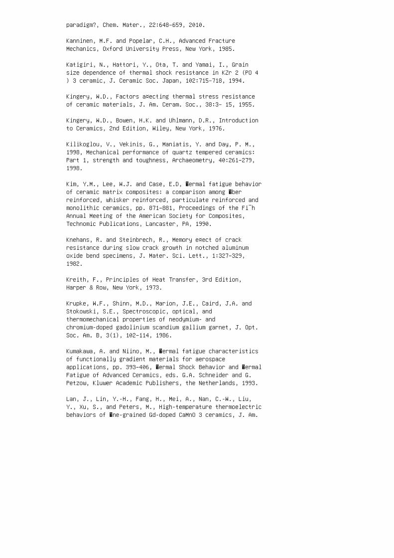
paradigm?, Chem. Mater., 22:648–659, 2010.
Kanninen, M.F. and Popelar, C.H., Advanced FractureMechanics, Oxford University Press, New York, 1985.
Katigiri, N., Hattori, Y., Ota, T. and Yamai, I., Grainsize dependence of thermal shock resistance in KZr 2 (PO 4) 3 ceramic, J. Ceramic Soc. Japan, 102:715–718, 1994.
Kingery, W.D., Factors a¤ecting thermal stress resistanceof ceramic materials, J. Am. Ceram. Soc., 38:3– 15, 1955.
Kingery, W.D., Bowen, H.K. and Uhlmann, D.R., Introductionto Ceramics, 2nd Edition, Wiley, New York, 1976.
Kilikoglou, V., Vekinis, G., Maniatis, Y. and Day, P. M.,1998, Mechanical performance of quartz tempered ceramics:Part 1, strength and toughness, Archaeometry, 40:261–279,1998.
Kim, Y.M., Lee, W.J. and Case, E.D, �ermal fatigue behaviorof ceramic matrix composites: a comparison among �berreinforced, whisker reinforced, particulate reinforced andmonolithic ceramics, pp. 871–881, Proceedings of the Fi¯hAnnual Meeting of the American Society for Composites,Technomic Publications, Lancaster, PA, 1990.
Knehans, R. and Steinbrech, R., Memory e¤ect of crackresistance during slow crack growth in notched aluminumoxide bend specimens, J. Mater. Sci. Lett., 1:327–329,1982.
Kreith, F., Principles of Heat Transfer, 3rd Edition,Harper & Row, New York, 1973.
Krupke, W.F., Shinn, M.D., Marion, J.E., Caird, J.A. andStokowski, S.E., Spectroscopic, optical, andthermomechanical properties of neodymium- andchromium-doped gadolinium scandium gallium garnet, J. Opt.Soc. Am. B, 3(1), 102–114, 1986.
Kumakawa, A. and Niino, M., �ermal fatigue characteristicsof functionally gradient materials for aerospaceapplications, pp. 393–406, �ermal Shock Behavior and �ermalFatigue of Advanced Ceramics, eds. G.A. Schneider and G.Petzow, Kluwer Academic Publishers, the Netherlands, 1993.
Lan, J., Lin, Y.-H., Fang, H., Mei, A., Nan, C.-W., Liu,Y., Xu, S., and Peters, M., High-temperature thermoelectricbehaviors of �ne-grained Gd-doped CaMnO 3 ceramics, J. Am.
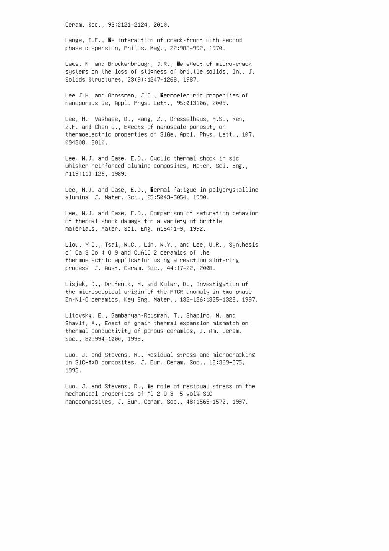
Ceram. Soc., 93:2121–2124, 2010.
Lange, F.F., �e interaction of crack-front with secondphase dispersion, Philos. Mag., 22:983–992, 1970.
Laws, N. and Brockenbrough, J.R., �e e¤ect of micro-cracksystems on the loss of sti¤ness of brittle solids, Int. J.Solids Structures, 23(9):1247–1268, 1987.
Lee J.H. and Grossman, J.C., �ermoelectric properties ofnanoporous Ge, Appl. Phys. Lett., 95:013106, 2009.
Lee, H., Vashaee, D., Wang, Z., Dresselhaus, M.S., Ren,Z.F. and Chen G., E¤ects of nanoscale porosity onthermoelectric properties of SiGe, Appl. Phys. Lett., 107,094308, 2010.
Lee, W.J. and Case, E.D., Cyclic thermal shock in sicwhisker reinforced alumina composites, Mater. Sci. Eng.,A119:113–126, 1989.
Lee, W.J. and Case, E.D., �ermal fatigue in polycrystallinealumina, J. Mater. Sci., 25:5043–5054, 1990.
Lee, W.J. and Case, E.D., Comparison of saturation behaviorof thermal shock damage for a variety of brittlematerials, Mater. Sci. Eng. A154:1–9, 1992.
Liou, Y.C., Tsai, W.C., Lin, W.Y., and Lee, U.R., Synthesisof Ca 3 Co 4 O 9 and CuAlO 2 ceramics of thethermoelectric application using a reaction sinteringprocess, J. Aust. Ceram. Soc., 44:17–22, 2008.
Lisjak, D., Drofenik, M. and Kolar, D., Investigation ofthe microscopical origin of the PTCR anomaly in two phaseZn-Ni-O ceramics, Key Eng. Mater., 132–136:1325–1328, 1997.
Litovsky, E., Gambaryan-Roisman, T., Shapiro, M. andShavit, A., E¤ect of grain thermal expansion mismatch onthermal conductivity of porous ceramics, J. Am. Ceram.Soc., 82:994–1000, 1999.
Luo, J. and Stevens, R., Residual stress and microcrackingin SiC–MgO composites, J. Eur. Ceram. Soc., 12:369–375,1993.
Luo, J. and Stevens, R., �e role of residual stress on themechanical properties of Al 2 O 3 -5 vol% SiCnanocomposites, J. Eur. Ceram. Soc., 48:1565–1572, 1997.
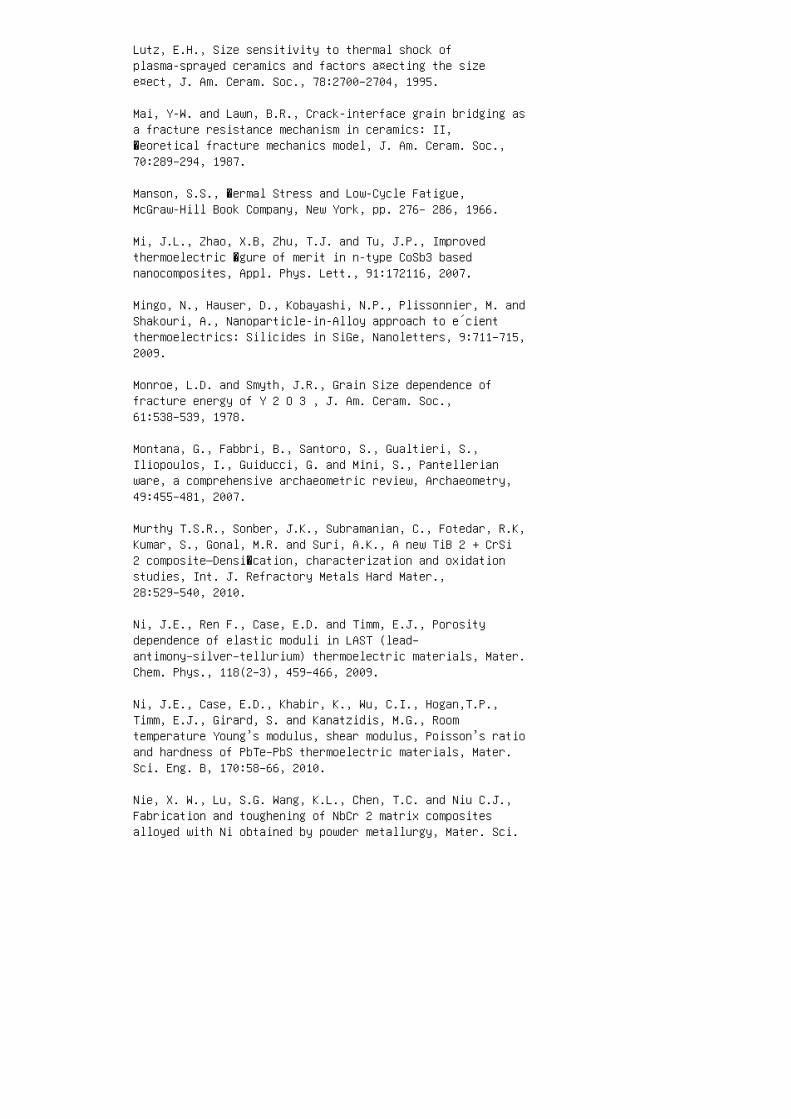
Lutz, E.H., Size sensitivity to thermal shock ofplasma-sprayed ceramics and factors a¤ecting the sizee¤ect, J. Am. Ceram. Soc., 78:2700–2704, 1995.
Mai, Y-W. and Lawn, B.R., Crack-interface grain bridging asa fracture resistance mechanism in ceramics: II,�eoretical fracture mechanics model, J. Am. Ceram. Soc.,70:289–294, 1987.
Manson, S.S., �ermal Stress and Low-Cycle Fatigue,McGraw-Hill Book Company, New York, pp. 276– 286, 1966.
Mi, J.L., Zhao, X.B, Zhu, T.J. and Tu, J.P., Improvedthermoelectric �gure of merit in n-type CoSb3 basednanocomposites, Appl. Phys. Lett., 91:172116, 2007.
Mingo, N., Hauser, D., Kobayashi, N.P., Plissonnier, M. andShakouri, A., Nanoparticle-in-Alloy approach to e´cientthermoelectrics: Silicides in SiGe, Nanoletters, 9:711–715,2009.
Monroe, L.D. and Smyth, J.R., Grain Size dependence offracture energy of Y 2 O 3 , J. Am. Ceram. Soc.,61:538–539, 1978.
Montana, G., Fabbri, B., Santoro, S., Gualtieri, S.,Iliopoulos, I., Guiducci, G. and Mini, S., Pantellerianware, a comprehensive archaeometric review, Archaeometry,49:455–481, 2007.
Murthy T.S.R., Sonber, J.K., Subramanian, C., Fotedar, R.K,Kumar, S., Gonal, M.R. and Suri, A.K., A new TiB 2 + CrSi2 composite—Densi�cation, characterization and oxidationstudies, Int. J. Refractory Metals Hard Mater.,28:529–540, 2010.
Ni, J.E., Ren F., Case, E.D. and Timm, E.J., Porositydependence of elastic moduli in LAST (lead–antimony–silver–tellurium) thermoelectric materials, Mater.Chem. Phys., 118(2–3), 459–466, 2009.
Ni, J.E., Case, E.D., Khabir, K., Wu, C.I., Hogan,T.P.,Timm, E.J., Girard, S. and Kanatzidis, M.G., Roomtemperature Young’s modulus, shear modulus, Poisson’s ratioand hardness of PbTe–PbS thermoelectric materials, Mater.Sci. Eng. B, 170:58–66, 2010.
Nie, X. W., Lu, S.G. Wang, K.L., Chen, T.C. and Niu C.J.,Fabrication and toughening of NbCr 2 matrix compositesalloyed with Ni obtained by powder metallurgy, Mater. Sci.
Eng. A, 502:85–90, 2009.
Noda, N., �ermal stresses in materials withtemperature-dependent properties, Appl. Mech. Rev., 44:383–397, 1991.
Norman, D.A. and Robertson, R.E., Rigid-particle tougheningof glassy polymers, Polymer, 44:2351–2362, 2003.
Nye, J.F., Physical Properties of Crystals, OxfordUniversity Press, New York, 1985.
Ohira, H. and Bradt, R.C., Strength distributions of aquench strengthened aluminosilicate ceramic, J. Am. Ceram.Soc., 71:35–41, 1988.
Padture, N.P., Gell, M. and Jordan, E.J., �ermal barriercoatings for gas-turbine engine applications, Science,296:280–284, 2002.
Park, K., Ko, K.Y., Seo, W.S., Cho, W.S., Kim, J.G. andKim, J.Y., High temperature thermoelectric properties ofpolycrystalline Zn 1–x−y Al x Ti y O ceramics, J. Euro.Ceram. Soc., 27:813–817, 2007.
Ravi, V., Firdosy, S., Calliat, T., Lerch, B., Calamino,A., Pawlik, R., Nathal, M., Sechrist, A., Buchhalter, J.and Nutt, S., Mechanical properties of thermoelectricskutterudites, pp. 656–662, Space Technology andApplications International Forum, American Institute ofPhysics, Melville, NY, 2008.
Ren, F., Case, E.D., Timm, E.J. and Schock, H.J., Young’smodulus as a function of composition for an N-typelead–antimony–silver–telluride (LAST) thermoelectricmaterial, Philos. Mag., 87(31):4907– 4934, 2007.
Ren, F., Case, E.D., Sootsman, J.R., Kanatzidis, M.G.,Kong, H., Uher, C., Lara-Curzio, E. and Trejo, R.M., �ehigh temperature elastic moduli of polycrystalline PbTemeasured by resonant ultrasound spectroscopy, Acta Mater.,56, 5954–5963, 2008a.
Ren, F., Case, E.D., Timm, E.J. and Schock, H.J., Hardnessas a function of composition for n-type LASTthermoelectric material, J. Alloys Compounds, 455:340–345,2008b.
Ren, F., Hall, B.D., Ni, J.E., Case, E.D., Timm, E.J.,Schock, H.J., Wu, C.-I., D’Angelo, J.J., Hogan, T.P.,
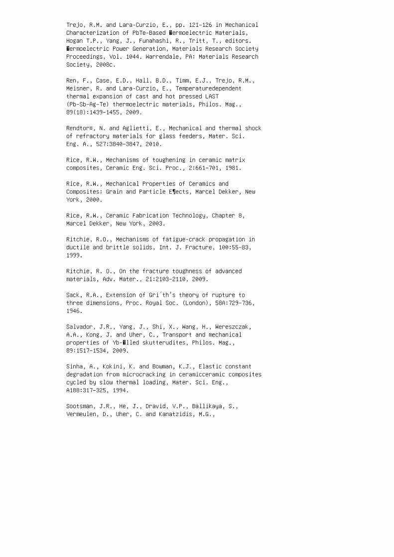
Trejo, R.M. and Lara-Curzio, E., pp. 121–126 in MechanicalCharacterization of PbTe-Based �ermoelectric Materials,Hogan T.P., Yang, J., Funahashi, R., Tritt, T., editors.�ermoelectric Power Generation, Materials Research SocietyProceedings, Vol. 1044. Warrendale, PA: Materials ResearchSociety, 2008c.
Ren, F., Case, E.D., Hall, B.D., Timm, E.J., Trejo, R.M.,Meisner, R. and Lara-Curzio, E., Temperaturedependentthermal expansion of cast and hot pressed LAST(Pb–Sb–Ag–Te) thermoelectric materials, Philos. Mag.,89(18):1439–1455, 2009.
Rendtor¤, N. and Aglietti, E., Mechanical and thermal shockof refractory materials for glass feeders, Mater. Sci.Eng. A., 527:3840–3847, 2010.
Rice, R.W., Mechanisms of toughening in ceramic matrixcomposites, Ceramic Eng. Sci. Proc., 2:661–701, 1981.
Rice, R.W., Mechanical Properties of Ceramics andComposites: Grain and Particle E¶ects, Marcel Dekker, NewYork, 2000.
Rice, R.W., Ceramic Fabrication Technology, Chapter 8,Marcel Dekker, New York, 2003.
Ritchie, R.O., Mechanisms of fatigue-crack propagation inductile and brittle solids, Int. J. Fracture, 100:55–83,1999.
Ritchie, R. O., On the fracture toughness of advancedmaterials, Adv. Mater., 21:2103–2110, 2009.
Sack, R.A., Extension of Gri´th’s theory of rupture tothree dimensions, Proc. Royal Soc. (London), 58A:729–736,1946.
Salvador, J.R., Yang, J., Shi, X., Wang, H., Wereszczak,A.A., Kong, J. and Uher, C., Transport and mechanicalproperties of Yb-�lled skutterudites, Philos. Mag.,89:1517–1534, 2009.
Sinha, A., Kokini, K. and Bowman, K.J., Elastic constantdegradation from microcracking in ceramicceramic compositescycled by slow thermal loading, Mater. Sci. Eng.,A188:317–325, 1994.
Sootsman, J.R., He, J., Dravid, V.P., Ballikaya, S.,Vermeulen, D., Uher, C. and Kanatzidis, M.G.,
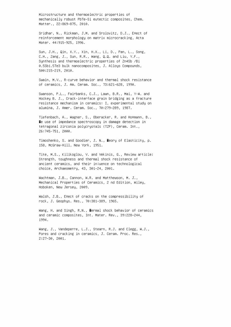
Microstructure and thermoelectric properties ofmechanically robust PbTe–Si eutectic composites, Chem.Matter., 22:869–875, 2010.
Sridhar, N., Rickman, J.M. and Srolovitz, D.J., E¤ect ofreinforcement morphology on matrix microcracking, ActaMater. 44:915–925, 1996.
Sun, J.H., Qin, X.Y., Xin, H.X., Li, D., Pan, L., Song,C.H., Zang, J., Sun, R.R., Wang, Q.Q. and Liu, Y.F.,Synthesis and thermoelectric properties of Zn4Sb /Bi0.5Sb1.5Te3 bulk nanocomposites, J. Alloys Compounds,500:215–219, 2010.
Swain, M.V., R-curve behavior and thermal shock resistanceof ceramics, J. Am. Ceram. Soc., 73:621–628, 1990.
Swanson, P.L., Fairbanks, C.J., Lawn, B.R., Mai, Y-W. andHockey B. J., Crack-interface grain bridging as a fractureresistance mechanism in ceramics: I, experimental study onalumina, J. Amer. Ceram. Soc., 70:279–289, 1987.
Tiefenbach, A., Wagner, S., Oberacker, R. and Ho¤mann, B.,�e use of impedance spectroscopy in damage detection intetragonal zirconia polycrystals (TZP), Ceram. Int.,26:745–751, 2000.
Timoshenko, S. and Goodier, J. N., �eory of Elasticity, p.158, McGraw-Hill, New York, 1951.
Tite, M.S., Kilikoglou, V. and Vekinis, G., Review article:Strength, toughness and thermal shock resistance ofancient ceramics, and their in¡uence on technologicalchoice, Archaeometry, 43, 301–24, 2001.
Wachtman, J.B., Cannon, W.R. and Matthewson, M. J.,Mechanical Properties of Ceramics, 2 nd Edition, Wiley,Hoboken, New Jersey, 2009.
Walsh, J.B., E¤ect of cracks on the compressibility ofrock, J. Geophys. Res., 70:381–389, 1965.
Wang, H. and Singh, R.N., �ermal shock behavior of ceramicsand ceramic composites, Int. Mater. Rev., 39:228–244,1994.
Wang, J., Vandeperre, L.J., Stearn, R.J. and Clegg, W.J.,Pores and cracking in ceramics, J. Ceram. Proc. Res.,2:27–30, 2001.
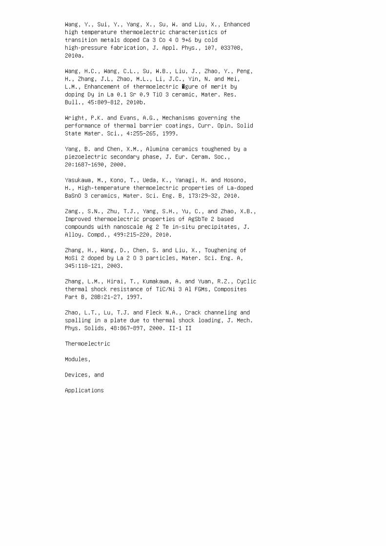
Wang, Y., Sui, Y., Yang, X., Su, W. and Liu, X., Enhancedhigh temperature thermoelectric characteristics oftransition metals doped Ca 3 Co 4 O 9+δ by coldhigh-pressure fabrication, J. Appl. Phys., 107, 033708,2010a.
Wang, H.C., Wang, C.L., Su, W.B., Liu, J., Zhao, Y., Peng,H., Zhang, J.L, Zhao, M.L., Li, J.C., Yin, N. and Mei,L.M., Enhancement of thermoelectric �gure of merit bydoping Dy in La 0.1 Sr 0.9 TiO 3 ceramic, Mater. Res.Bull., 45:809–812, 2010b.
Wright, P.K. and Evans, A.G., Mechanisms governing theperformance of thermal barrier coatings, Curr. Opin. SolidState Mater. Sci., 4:255–265, 1999.
Yang, B. and Chen, X.M., Alumina ceramics toughened by apiezoelectric secondary phase, J. Eur. Ceram. Soc.,20:1687–1690, 2000.
Yasukawa, M., Kono, T., Ueda, K., Yanagi, H. and Hosono,H., High-temperature thermoelectric properties of La-dopedBaSnO 3 ceramics, Mater. Sci. Eng. B, 173:29–32, 2010.
Zang., S.N., Zhu, T.J., Yang, S.H., Yu, C., and Zhao, X.B.,Improved thermoelectric properties of AgSbTe 2 basedcompounds with nanoscale Ag 2 Te in-situ precipitates, J.Alloy. Compd., 499:215–220, 2010.
Zhang, H., Wang, D., Chen, S. and Liu, X., Toughening ofMoSi 2 doped by La 2 O 3 particles, Mater. Sci. Eng. A,345:118–121, 2003.
Zhang, L.M., Hirai, T., Kumakawa, A. and Yuan, R.Z., Cyclicthermal shock resistance of TiC/Ni 3 Al FGMs, CompositesPart B, 28B:21–27, 1997.
Zhao, L.T., Lu, T.J. and Fleck N.A., Crack channeling andspalling in a plate due to thermal shock loading, J. Mech.Phys. Solids, 48:867–897, 2000. II-1 II
Thermoelectric
Modules,
Devices, and
Applications
17 Chapter 17 - MiniaturizedThermoelectric Converters, Technologies,and Applications
1. Fleurial, J.-P., Borshchevsky, A., Ryan, M.A., Phillips,W., Kolawa, E., Kacisch, T., Ewell, R. �ermoelectricmicrocoolers for thermal management applications, Proc 16thInt. Conf. �ermoelectrics, Dresden, Germany, August 1997,pp. 641–645.
2. Böttner, H., Nurnus, J., Schubert, A. Miniaturizedthermoelectric converters. In: D.M. Rowe (ed.),�ermoelectrics Handbook: Macro to Nano-StructuredMaterials, Taylor & Francis, Boca Raton, FL, 2006, pp.46.1–46.18.
3. Chowdhury, I., Prasher, R., Lofgreen, K., Chrysler, G.,Narasimhay, S., Mahajan, R., Koester, D., Alley, R.,Venkatasubramanian, R. On-chip cooling bysuperlattice-based thin-�lm thermoelectrics, Nat.Nanotechnology, pub. online: 25 January 2009 | DOI:10.1038/NNANO.2008.417.
4. Böttner, H., Nurnus, J., Gavrikov, A., Kühner, G.,Jägle, M., Künzel, C., Eberhard, D., Plescher, G.,Schubert, A., Schlereth, K.-H. New thermoelectriccomponents using microsystem technologies, JMEMS 13 (3),414–420, 2004.
5. Nurnus, J.�ermoelectric thin �lm power generators: Selfsu´cient power supply for smart systems, Smart Sensors,Actuators and MEMS IV, Proc. SPIE, Dresden, Germany, May4–6 2009, Vol. 7362, pp. 736205-1.
6. Hudak, N-.S., Amatucci, G.-G. Small-scale energyharvesting through thermoelectric, vibration, andradiofrequency power conversion. JAP, 1003, 101301, 2008.
7. Frost and Sullivan. Advances in Energy HarvestingTechnologies, DoC2, December 2007.
8. Venkatasubramanian, R. �in-�lm thermoelectric device andfabrication method of same, US 6,300,150 B1. October 92001.
9. Venkatasubramanian, R., Siivola, E., Colpitts, T.,OQuinn, B. �in-�lm thermoelectric devices with highambient-temperature �gures of merit, Nature 413, 597–602,2001.
10. http://www.micropelt.com/, 13.01.2011.
11. Schlereth, K.H., Böttner, H., Schubert, A., Acklin, B.Verfahren zum Herstellen eines thermoelektrischen Wandlers,DE0019845104A1, p. date: September 30. 1998.
12.
13.
14. Semenyuk, V.A. Advances in development ofthermoelectric modules for cooling electro-opticcomponents, Proc 22nd Int. Conf. �ermoelevtrics, pp.631–636, La Grand Motte, France, 2003.
15. Böttner, H., Ebling, D., Jacquot, A., König, J.,Kirste, L., Schmidt, J. Structural and mechanicalproperties of spark plasma sintered n- and p-type bismuthtelluride alloys, Phys. Stat. Sol. (RRL) 1(6), 235–237,2007.
16. Böttner, H., Nurnus, J., Schubert, A., Volkert, F. Newhigh density micro structured thermogenerators for standalone sensor systems, Proc 26th Int. Conf. �ermoelectrics,Jeju, Korea, June 2007, pp. 311–314.
17. Enocean: http://www.enocean.com/de/white_papers/13.01.2011.
18. Glatz, W., Schwyter, E., Durrer, L., and Hierold, Ch.Bi 2 Te 3 -based ¡exible micro thermoelectric generatorwith optimized design, JMEMS, 18, 763–772, 2009.
19. Stordeur, M., Stark, I. Low power thermoelectricgenerator-self-su´cient energy supply for micro systems,Proc. 16th Int. Conf. �ermoelectrics, Dresden, Germany,August 1997, pp. 575–577.
20. Goncalves, L.M., Rocha, J.G., Couto, C., Alpuim, P.,Gao Min, Rowe, D.M., Correia, J.H. Fabrication of ¡exiblethermoelectric microcoolers using planar thin-�lmtechnologies, JMM, 17, 168–173, 2006.
21. Rocha, R.P. Carmo, J.P., Goncalves, L.M., Correia, J.H.An energy scavenging microsystem based onthermoelectricity for battery life extension in laptops,Proc 35th Annual Conference of IEEE Industrial Electronics(IECON 2009), 2009, pp. 1813–1816.
22. Boulanger, C. �ermoelectric material electroplating: A
historical review, JEMS, 39(9), 1818–1827, 2010, DOI:10.1007/s11664-010-1079-6.
23. www.micropelt.com, 12.01.2011
24. Rowe, D.M. Miniature semiconductor thermoelectricdevices. In: D.M. Rowe (ed.), CRC Handbook of�ermoelectrics, Taylor & Francis, Boca Raton, 1995, pp.441–458.
25. Nextreme �ermal Solutions, White paper: �e thermalcopper pillar bump: Enabling improved semiconductorperformance without sacri�cing e´ciency, Nextreme �ermalSolutions, January 9, 2008.
26. Nurnus, J. State of art thermoelectric thin �lmdevices, NanoS—�e Nanotech Journal 01.08, WileyVCH Verlag,Weinheim, pp. 11–15, 2008.
27. Venkatasubramanian, R., Siivola, E., T. O’Quinn. In:D.M. Rowe (ed.), �ermoelectrics Handbook: Macro to Nano,Taylor & Francis, Boca Raton, FL, 2006, pp. 46.1–46.18.
28.
29. http://www.micropelt.com/products/datasheets.php,06.02.2011.
30.
31. http://www.micropelt.com/products/mypelt.php,06.02.2011.
32.http://www.micropelt.com/down/datasheet_mpc_d403_d404.pdf,06.02.201.
33. http://www.micropelt.com/down/cooling_and_heating.pdf,06.02.2011.
34.
35. http://www.micropelt.com/applications/biomedical.php,06.02,2011.
36. Baier, M. Temperatursonde für einen Ofen, Ofen undVerfahren zum Betrieb eines Ofens, WO 2008/119440 A2,09.10.2008.
37. Bartholome, K., Bartel, M., Binninger, R., Schumacher,
I., Schröder, H., Ebling, D. Energy-autarkic sensortechnology in aircra¸, Proc 8th ECT, Como, Italy,September. 2010.
38. Su, J., Vullers, R.J.M., Goedbloed, M., van Andel, Y.,Leonov, V., Wang, Z. �ermoelectric energy harvesterfabricated by stepper, Micro Eng, 87, 1242–1244, 2010.
39. Patent EP 1976034.
40. Van Andel, Y., Jambunathan, M., Vullers, R.J.M.,Leonov, V. Membrane-less in-plane bulk-micromachinedthermopiles for energy harvesting, Micro Eng, 78,1294–1296, 2010.
41.
42.
43. http://www.nextreme.com/thermalcharger, 06.02.2011.
44.http://www.micropelt.com/applications/te_power_node.php,06.02.2011.
45.http://www.st.com/internet/com/press_releases/t3020.jsp,06.02.2011.
46. Fräulin, C., Nurnus, J. Energy autonomous sensorsystems for automotive condition monitoring, 2ndInternational Conference: �ermoelectrics Goes Automotive,Berlin, Germany, 9–10.12.2010.
47.
48.
49.
18 Chapter 18 - Application ofThermoelectrics for Thermal Managementof High-Power Microelectronics
1. Chu, R.C. and Simons, R.E. 1999. Application ofthermoelectrics to cooling electronics: Review andprospects, Proc. 18th Int. Conf. �ermoelectrics, 270–9.Baltimore: IEEE.
2. Bierschenk, J. and Gilley, M. 2006. Assessment of TECthermal and reliability requirements forthermoelectrically enhanced heat sinks for CPU coolingapplications, Proc. 25th Int. Conf. �ermoelectrics, pp.254–9. Vienna, Austria: IEEE.
3. Yu, C.-K., Liu, C.-K., Dai, M.-J. et al. 2007. Athermoelectric cooler integrated with IHS on a FC-PBGApackage, Proc. 26th Int. Conf. �ermoelectrics, pp. 279–83.Jeju, Korea: IEEE.
4. Yamaguchi, S., Fukuda, S., Kitagava, H. et al. 2008. Anew proposal of Peltier cooling for microprocessor, Proc.27th Int. Conf. �ermoelectrics, Corvallis, Oregon: IEEE.http://kamome.lib.ynu.ac.jp/dspace/bitstream/10131/5064/1/ICT2008IB1.pdf
5. Ikeda, M., Nakamura, T., Kimura, Y. et al. 2006. �ermalperformance of thermoelectric cooler (TEC) integrated heatsink and optimizing structure for low acoustic noise/powerconsumption, Proc. 22th IEEE Semi-�erm Symposium, pp.144–51. Dallas, TX: IEEE Xplore Digital Library. http://
6. Sauciuc, I., Prasher, R., Chang, J.Y. et al. 2005.�ermal performance and key challenges for future CPUcooling technologies, Proc. ASME InterPACK, pp. 353–64. SanFrancisco: ASME.
7. Semenyuk, V.A. and Dekhtiaruk, R.I. 2007. �ermoelectriccooling under dimensional constraints, Journal of�ermoelectricity 4: 69–75.
8. Semenyuk, V.A. and Dekhtyaruk, R.I. 2010. Prospects forthermal management of powerful microprocessors usingthermoelectrics, Proc. 8th European Conf. �ermoelectrics,pp. 106–11. Como, Italy.
9. Semenyuk, V.A. and Dekhtiaruk, R.I. 2010. �ermoelectriccooling of powerful microprocessors, Journal of�ermoelectricity 4: 67–76.
10. Intel Corporation. 2009. Intel Core i7-800 and i5-700desktop processor series and LGA1156 socket:�ermal/mechanical speci�cations and design guidelines.http://download. intel.com/design/processor/datashts/322164.pdf
11. Wang, P., Bar-Cohen, A., and Yang, B. 2007. Enhancedthermoelectric cooler for on-chip hot spot cooling, Proc.of IPACK2007, Paper No: IPACK2007-33798, pp. 249–58.Vancouver: ASME.
12. Lee, K.H. and Kim, O.J. 2007. Simulation of the coolingsystem using thermoelectric micro-coolers for hot spotmitigation, Proc. 26th Int. Conf. on �ermoelectrics, pp.284–87. Jeju, Korea: IEEE.
13. Kim, O.J. and Lee, K.H. 2007. A study on theapplication of micro TEC for hot spot cooling, Proc. 26thInt. Conf. on �ermoelectrics, pp. 344–47. Jeju, Korea:IEEE.
14. Semenyuk, V.A. and Protsenko, D. 2008. On-chip hot spotcooling: Forecasts and reality, Proc. 6th European Conf.�ermoelectrics, I-06, pp. 1–6. Paris.
15. Arctic Silver, Inc. 2007. High-density polysyntheticsilver thermal compound Arctic Silver 5. http://www.arcticsilver.com/as5.htm (accessed January 07, 2011).
16. Venkatasubramanian, R., Sivola, E., and O’Quinn, B.2006. Superlattice thin-�lm thermoelectric material anddevice technologies, �ermoelectrics Handbook: Macro toNano, ed. D.M. Rowe, Chapter 49, pp. 1–15. Boca Raton, CRCPress.
17. Böttner, H., Nurnus, J., and Schubert, A. 2006.Miniaturized thermoelectric converters, �ermoelectricsHandbook: Macro to Nano, ed. D.M. Rowe, Chapter 46, pp.1–18. Boca Raton, CRC Press.
18. Nextreme, Inc. 2010. Micro-scale thermal and powermanagement: Cooling & temperature control.
19 Chapter 19 - Millikelvin TunnellingRefrigerators
Anghel, D. V. and Pekola, J. P., Noise in refrigeratingtunnel junctions and in microbolometers, Journal of LowTemperature Physics, 123(3–4) 197, 2001.
Bardas, A. and Averin, D., Peltier e¤ect innormal-metal–superconductor microcontacts, Physical ReviewB, 52(17) 12873, 1995.
Clark, A. M., Miller, N. A., Williams, A., Ruggiero, S. T.,Hilton, G. C., Vale, L. R., Beall, J. A., Irwin, K. D.,and Ullomb, J. N., Cooling of bulk material byelectron-tunneling refrigerators, Applied Physics Letters,86 173508, 2005.
Clark, A. M., Williams, A., Ruggiero, S. T., van den Berg,M. L., and Ullom, J. N., Practical electron- tunnelingrefrigerator, Applied Physics Letters, 84 625, 2004.
Dynes, R. C., Garno, J. P., Hertel, G. B., and Orlando, T.P., Tunneling study of superconductivity near themetal-insulator transition, Physical Review Letters, 532437, 1984.
Edwards, H. L., Niu, Q., Georgakis, G. A., and de Lozanne,A. L., Cryogenic cooling using tunneling structures withsharp energy features, Physical Review B, 52(8) 5714, 1995.
Fisher, P. A., Ullom, J. N., and Nahum, M., High-poweron-chip microrefrigerator based on anormalmetal/insulator/superconductor tunnel junction,Applied Physics Letters, 74 2705, 1999.
Frank, B. and Kretch, W., Electronic cooling insuperconducting tunnel junctions, Physics Letters A, 235281, 1997.
Giazotto, F., Heikkila, T. T., Luukanen, A., Savin, A. M.,and Pekola, J., Opportunities for mesoscopics inthermometry and refrigeration: Physics and applications,Review of Modern Physics, 78 217, 2006a.
Giazotto, F., Taddei, F., Fazio, R., and Beltram, F.,Ultrae´cient cooling in ferromagnet–superconductormicrorefrigerators, Applied Physics Letters, 80(20) 3784,2002.
Giazotto, F., Taddei, F., Governale, M., Castellana, C.,
Fazio, R., and Beltram, F., Cooling electrons bymagnetic-�eld tuning of Andreev re¡ection, Physical ReviewLetters, 97 197001, 2006b.
Golubev, D. and Kuzmin, L., Nonequilibrium theory of ahot-electron bolometer with normalmetalinsulator-superconductor tunnel junction, Journal ofApplied Physics, 89 6464, 2001.
Jochum, J., Mears, C., Golwala, S., Sadoulet, B., Castle,J. P., Cunningham, M. F., Drury, O. B. et al., Modelingthe power ¡ow in normal conductor-insulator-superconductorjunctions, Journal of Applied Physics, 83(6) 3217, 1998.
Jug, B. and Trontelj, Z., Electronic refrigerators:Optimization studies, IEEE Transactions on AppliedSuperconductivity, 9(2) 4483, 1999.
Kivinen, P., Savin, A., Zgirski, M., Törmä, P., Pekola, J.,Prunnila, M., and Ahopelto, J., Electron–phonon heattransport and electronic thermal conductivity in heavilydoped silicon-on-insulator �lm, Journal of AppliedPhysics, 94(5) 3201, 2003.
Kuzmin, L. and Golubev, D., On the concept of an optimalhot-electron bolometer with NIS tunnel junctions, PhysicaC, 372–376 378, 2002.
Leivo, M. M., Manninen, A. J., and Pekola, J. P.,Microrefrigeration by normal-metal/insulator/superconductortunnel junctions, Applied Superconductivity, 5 227, 1998.
Leivo, M. M., Pekola, J. P., and Averin, D. V., E´cientPeltier refrigeration by a pair ofnormal-metal/insulator/superconductor junctions, AppliedPhysics Letters, 68(14) 1996, 1996.
Leoni, R., On-chip micro-refrigerators for sub-Kelvincooling, New Astronomy Review, 43 317, 1999.
Leoni, R., Arena, G., Castellano, M. G., and Torrioli, G.,Electron cooling by arrays of submicron tunnel junctions,Journal of Applied Physics, 85(7) 3877, 1999.
Li, L., Frunzio, L., Wilson, C., Prober, D. E., Szymkowiak,A. E., and Moseley, S. H., Improved energy resolution ofx-ray single photon imaging spectrometers usingsuperconducting tunnel junctions, Journal of AppliedPhysics, 90 3645, 2001.
Luukanen, A., Leivo, M. M., Suoknuuti, J. K., Manninen, A.J., and Pekola, J. P., On-chip cefrigeration byevaporation of hot electrons at sub-Kelvin temperatures,Journal of Low Temperature Physics, 120 281, 2000.
Manninen, A. J., Leivo, M. M., and Pekola, J. P.,Refrigeration of a dielectric membrane by
Muhonen, J. T., Niskanen, A. O., Meschke, M., Pashkin, Yu.A., Tsai, J. S., Sainiemi, L., Franssila, S., and Pekola,J. P., Electronic cooling of a submicron-sized metallicbeam, Applied Physics Letters, 94 073101, 2009.
Muhonen, J. T., Prest, M. J., Prunnila, M., Gunnarsson, D.,Dobbie, A., Myronov, M., Whall, T. E., Parker, E. H. C.,and Leadley, D. R., Strain dependence of electron-phononenergy loss rate in many-valley semiconductors, AppliedPhysics Letters, 98(18) 182103, 2011.
Nahum, M., Eiles, T. M., and Martinis, J. M., Electronicmicrorefrigerator based on a normal-insulatorsuperconductortunnel junction, Applied Physics Letters, 65 3123, 1994.
Nahum, M. and Martinis, J. M., Ultrasensitive-hot-electronmicrobolometer, Applied Physics Letters, 63 3075, 1993.
Miller, N. A., Clark, A. M., Williams, A., Ruggiero, S. T.,Hilton, G. C., Beall, J. A., Irwin, K. D., Vale, L. R.,and Ullom, J. N., Measurements and modeling of phononcooling by electron-tunneling refrigerators, IEEETransactions on Applied Superconductivity, 15 556, 2005.
Miller, N. A., O’Neil, G. C., Beall, J. A., Hilton, G. C.,Irwin, K. D., Schmidt, D. R., Vale, L. R., and Ullom, J.N., High resolution x-ray transition-edge sensor cooled bytunnel junction refrigerators, Applied Physics Letters, 92163501, 2008.
Pekola, J., Tunnelling into the chill, Nature, 435 889,2005.
Pekola, J. P., Anghel, D. V., Suppula, T. I., Suoknuuti, J.K., and Manninen, A. J., Trapping of quasiparticles of anonequilibrium superconductor, Applied Physics Letters, 76(19) 2782, 2000a.
Pekola, J. P., Heikkila, T. T., Savin, A. M., Flyktman, J.T., Giazotto, F., and Hekking, F. W. J., Limitations incooling electrons using normal-metal-superconductor tunneljunctions, Physical Review Letters, 92 056804–1, 2004a.
Pekola, J. P., Manninen, A. J., Leivo, M. M., Arutyunov,K., Suoknuuti, J. K., Suppula, T. I., and Collaudin, B.,Microrefrigeration by quasiparticle tunnelling in NIS andSIS junctions, Physica B, 280 485, 2000b.
Pekola, J. P., Schoelkopf, R., and Ullom, J. N., Cryogenicson a chip, Physics Today, May 41, 2004b.
Rajauria, S., Gandit, P., Fournier, T., Hekking, F. W. J.,Pannetier, B., and Courtois, H., Andreev currentinduceddissipation in a hybrid superconducting tunnel junction,Physical Review Letters, 100 207002, 2008.
Roukes, M. L., Freeman, M. R., Germain, R. S., andRichardson, R. C., Hot electrons and energy transport inmetals at millikelvin temperatures, Physical ReviewLetters, 55 422, 1985.
Rowell, J. M. and Tsui, D. C., Hot electron temperature inInAs measured by tunneling, Physical Review B, 14(6) 2456,1976.
Savin, A., Pekola, J., Prunnila, M., Ahopelto, J., andKivinen, P., Electronic cooling and hot electron e¤ects inheavily doped silicon-on-insulator �lm, Physica Scripta,T114 57, 2004.
Savin, A., Prunnila, M., Ahopelto, J., Kivinen, P., Torma,P., and Pekola, J., Application ofsuperconductor–semiconductor Schottky barrier for electroncooling, Physica B, 329–333 1481, 2003.
Savin, A., Prunnila, M., Kivinen, P. P., Pekola, J. P.,Ahopelto, J., and Manninen, A. J., E´cient electroniccooling in heavily doped silicon by quasiparticletunneling, Applied Physics Letters, 79 (10) 1471, 2001.
Solymar, L., Superconductive Tunnelling and Applications(Chapman & Hall, London), 1972.
Tinkham, M., Introduction to Superconductivity, 2nd ed.(McGraw-Hill, New York), 1996.
Ullom, J. N., Fisher, P. A., and Nahum, M., Measurements ofquasiparticle thermalization in a normal metal, PhysicalReview B, 61 14839, 2000.
Ullom, J. N., van den Berg, M. L., and Labov, S. E., A newidea for a solid-state microrefrigerator operating near
100 mK, IEEE Transactions on Applied Superconductivity, 11639, 2001.
Wellstood, F. C., Urbina, C., and Clarke, J., Hot electrone¤ects in metals, Physical Review B, 49 5942, 1994.
20 Chapter 20 - Heat Dissipaters
1. Biercuk, M. J., Llaguno, M. C., Radosavljevic, M., Hyun,J. K., Johnson, A. T., and Fischer, J. E., Heat transferin carbon nanotube composites. Applied Physics Letters, 80,2767–2769, 2002.
2. Berber, S., Young-Kyun, K., and Tománek, D. Unusuallyhigh thermal conductivity of carbon nanotubes. PhysicalReview Letters, 84, 2000.
3. Rohsenow, W. M., Handbook of Heat Transfer, McGraw Hill,New York, 1987.
4. Chapman, A., Heat Transfer, Collier McMillan Co.,Madrid, 1977.
5. Incropera, F. P. and De Witt, D. P. Introduction to HeatTransfer, John Wiley & Sons, New York, 1990.
6. Madhusudana, C. V., �ermal Contact Conductance,Springer, New York, 1992.
7. Yovanovich, M. M., Culham, J. R., and Teertstra, P.,Calculating interface resistance. Electronics Cooling,3(2), 24–29, 1997.
8. Chung, D. D. L., Materials for thermal conduction,Applied �ermal Engineering, 21, 1593–1605, 2001.
9. Prasher, R., �ermal Interface materials: Historicalperspective, status and future directions. Proceedings ofthe IEEE. 98(8), 1571–1586, 2006.
10. Neubauer, E. and Korb, G., �e in¡uence of mechanicaladhesion of copper coatings on carbon surfaces on theinterfacial thermal contact resistance, �in Solid Films.,433(1–2), 160–165, 2003.
11. Lahmar, A. and Nguyen, T. P., Experimentalinvestigation on the thermal contact resistance betweengold coating and ceramic substrates. �in Solid Films,389(1–2), 167–172, 2001.
12. Wolf, E. G. and Schneider, D. A., Prediction of thermalcontact resistance between polished surfaces.International Journal of Heat and Mass Transfer, 41(22),3469–3482, 1998.
13. Marlow, R., Buist, R. J., and Nelson, J. L.,
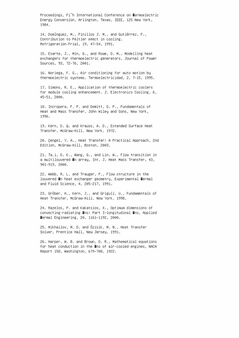
Proceedings, Fi¯h International Conference on �ermoelectricEnergy Conversion, Arlington, Texas, IEEE, 125 New York,1984.
14. Domínguez, M., Pinillos J. M., and Gutiérrez, P.,Contribution to Peltier e¤ect in cooling.Refrigeration-Frial, 19, 47–54, 1991.
15. Esarte, J., Min, G., and Rowe, D. M., Modelling heatexchangers for thermoelectric generators, Journal of PowerSources, 93, 72–76, 2001.
16. Noriega, F. G., Air conditioning for auto motion bythermoelectric systems. Termoelectricidad, 2, 7–15, 1995.
17. Simons, R. E., Application of thermoelectric coolersfor module cooling enhancement. J. Electronics Cooling, 6,45–51, 2000.
18. Incropera, F. P. and DeWitt, D. P., Fundamentals ofHeat and Mass Transfer, John Wiley and Sons, New York,1996.
19. Kern, D. Q. and Krauss, A. D., Extended Surface HeatTransfer. McGraw-Hill. New York. 1972.
20. Çengel, Y. A., Heat Transfer: A Practical Approach, 2ndEdition, McGraw-Hill, Boston, 2003.
21. Ta¸i, D. K., Wang, G., and Lin, W., Flow transition ina multilouvered �n array, Int. J. Heat Mass Transfer, 43,901–919, 2000.
22. Webb, R. L. and Trauger, P., Flow structure in thelouvered �n heat exchanger geometry, Experimental �ermaland Fluid Science, 4, 205–217, 1991.
23. Gröber, H., Kern, J., and Grigull, U., Fundamentals ofHeat Transfer, McGraw-Hill. New York. 1998.
24. Razelos, P. and Kakatsios, X., Optimum dimensions ofconvecting-radiating �ns: Part I—longitudinal �ns, Applied�ermal Engineering, 20, 1161–1192, 2000.
25. Mikhailov, M. D. and Özisik, M. N., Heat TransferSolver, Prentice Hall, New Jersey. 1991.
26. Harper, W. B. and Brown, D. R., Mathematical equationsfor heat conduction in the �ns of air-cooled engines, NACAReport 158, Washington, 679–708, 1922.
27. Guyer, E. C. and Brownell, D. L. Handbook of Applied�ermal Design, McGraw-Hill. New York, 1989.
28. Söylemez, M. S., On the optimum heat exchanger sizingfor heat recovery, Energy Conversion & Management, 41,1419–1427, 2000.
29. Yeh, H., Analytical study of the optimum dimensions ofrectangular �ns and cylindrical pin �ns, Int. J. Heat MassTransfer, 40, 3607–3615, 1997.
30. Reklaitis, G. V., Ravindran, A., and Ragsdell, K. M.,Engineering Optimization, Methods and Applications, JohnWiley and Sons, New Jersey, 1983.
31. Gardner, K. A., E´ciency of extended surfaces. Trans.ASME, 69(8), 621–631, 1945.
32. Holman, J. P., Heat Transfer, McGraw-Hill. New York,1998.
33. Çengel, Y. A., Heat Transfer, McGraw-Hill. New York,2004.
34. Blanco, J. M., Sala, J. M., and López, L. M.,Tecnología energética, Servicio de publicaciones de laEscuela Superior de Ingenieros de Bilbao, 2004.
35. Zukauskas, A. and Ulinskas, R., Banks of plain and�nned tubes, Heat Exchanger Design Handbook, G. F. HewittEdition, Begell House, Inc., New York, 1998.
36. Rich, D. G., �e e¤ect of �n spacing on the heattransfer and friction performance of multi-row, Smoothplate �nned-tube heat exchangers, ASHRAE Transactions,79(2), 137–145, 1973.
37. Sunubu, J. H., �e e¤ect of spacing on the e´ciency ofextended surfaces for natural convection cooling.Proceedings of the National Electronics Packaging andProduction Conference, New York, 1963.
38. Christopher, A. S., �ermshield, L. L. C., and Laconia,N. H., Optimize �n spacing: How close is too close? PowerElectronics Technology, 8, 35–43, 2006.
39. Kraus, A. D. and Bar-Cohen, A., �ermal Analysis andControl of Electronic Equipment, McGrawHill, New York,1983.
40. Girón-Palomares, B. et al., Optimización y análisis dearreglos de aletas rectangular, triangular, parabólicoconvexo, anulares (hiperbólico, triangular, rectangular) yal�ler, Revista Iberoamericana de Ingeniería Mecánica,10(3), 33–39, 2006.
41. Elmahdy, A. H. and Biggs, R. C., E´ciency of extendedsurfaces with simultaneous heat and mass transfer, ASHRAETransactions, V 1, 135–143, 1983.
42. Kraus, A. D., Aziz, A., and Welty, J., Extended surfaceheat transfer, Appl. Mech. Rev., 54(5), 97–117, 2001.
43. Ünal, H. C., Determination of the temperaturedistribution in an extended surface with a non-uniform heattransfer coe´cient. International Journal of Heat and MassTransfer, 28(12), 2279–2284, 1985.
44. Yan, Z. and Holmstedt, G., A fast narrow band computermodel for radiation calculations. Numerical Heat TransferPart B: Fundamentals, 31, 61–71, 1997.
45. Launder, B. E. and Spalding, D. B., �e NumericalComputation of Turbulent Flows, Imperial College ofScience and Technology, London, England, NTIS N74-12066,1973.
46. Faghri, A., Heat Pipe Science and Technology, Taylor &Francis, New York, 2000.
47. Michael, J. and Ellsworth, Jr., Comparing liquidcoolants from both a thermal and hydraulic perspective.Electronics Cooling, 12(3), 36–38, 2006.
48. Reay, D. and Kew, P., Heat Pipes: �eory, Design andApplications, BH Elsevier, Edinburgh, 2006.
49. Scott, D., Heat pipes for electronics coolingapplications. Electronics Cooling, 2(3), 18–23, 1996.
50. Esarte, J., Wolluscheck, C., and Armendariz, E., Phasechange dissipater of aluminium container. THERMINICConference, Rome, 2008.
51. Jinwang L., Yong Z., and Cheng, L., Experimental studyon capillary pumping performance of porous wicks for loopheat pipe. Experimental �ermal and Fluid Science, 34(8),1403–1408, 2010.

52. Xiao, H. and Franchi, G., Design and fabrication ofhybrid bi-modal wick structure for heat pipe application.Journal of Porous Materials, 15(6), 635–642, DOI:10.1007/s10934-007-9143-1.
53. Yu, F. and Maydanik, K., Review loop heat pipes,Applied �ermal Engineering, 25, 635–657, 2005.
21 Chapter 21 - Thin-Film SuperlatticeThermoelectric Devices for EnergyHarvesting and Thermal Management
1. M. Dresselhaus, T. Harman, and R. Venkatasubramanian,Proc. of the 1st �ermogenic Workshop, Ft. Belvoir, VA,Ed., S. Horn, 1992.
2. R. Venkatasubramanian, E. Siivola, T. Colpitts, and B.O’Quinn, �in-�lm thermoelectric devices with highroom-temperature �gures of merit. Nature 413, 597–602,2001.
3. T.C. Harman, P.J. Taylor, M.P. Walsh, and B.E. LaForge,Quantum dot superlattice thermoelectric materials anddevices. Science 297, 2229–2232, 2002.
4. K. Hsu, S. Loo, F. Guo, W. Chen, J. Dyck, C. Uher, T.Hogan, E. Polychroniadis, and M. Kanatzidis, Science 303,818, 2004.
5. W. Kim, J. Zide, A. Gossard, D. Klenov, S. Stemmer, A.Shakouri, and A. Majumdar, Phys. Rev. Lett. 96, 045901,2006.
6. A.I. Hochbaum, R.K. Chen, R.D. Delgado, W.J. Liang, E.C.Garnett, M. Najarian, A. Majumdar, and P.D. Yang, Nature451, 163–168, January 2008.
7. A.I. Boukai, Y. Bunimovich, J. Tahir-Kheli, J.K. Yu,W.A. Goddard, and J.R. Heath, Nature 451, 168– 171, January2008.
8. R. Venkatasubramanian, Bull. Am. Phys. Soc. 41, 693,1996; See also Naval Research Reviews 48(4), 31, 1996; R.Venkatasubramanian and T. S. Colpitts, in �ermoelectricMaterials—New Directions and Approaches, p. 73, Eds. T.M.Tritt, M. Kanatzidis, and H.B. Lyon, Mat. Res. Soc.Proceedings No. 478, Pittsburgh, 1997.
9. S. M. Lee, D.G. Cahill, and R. Venkatasubramanian, Appl.Phys. Lett. 70, 2957, 1997.
10. G. Chen, Phys. Rev. B 57, 14958, 1998.
11. M.V. Simkin and G.D. Mahan, Phys. Rev. Lett. 84, 927,2000.
12. R. Venkatasubramanian, Phys. Rev. B 61, 3091, 2000.
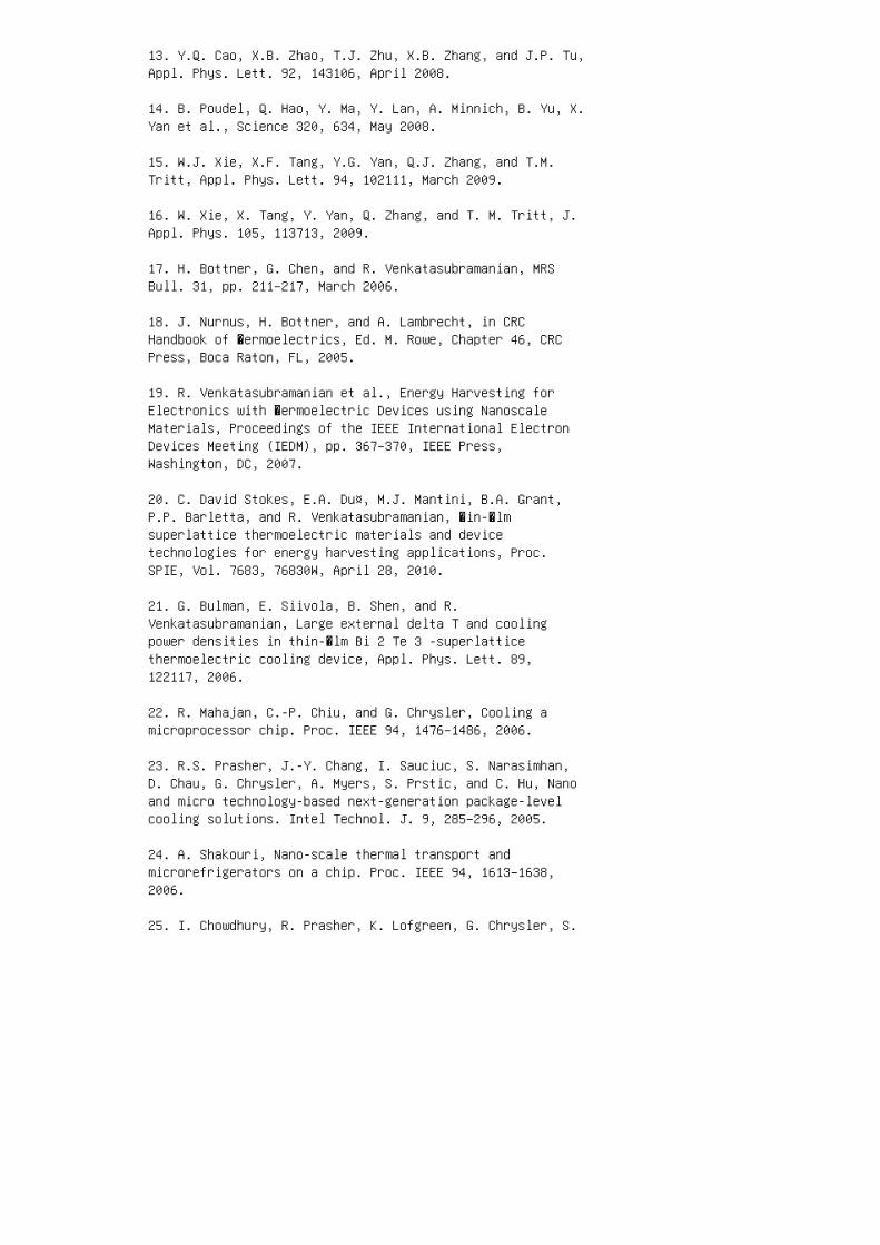
13. Y.Q. Cao, X.B. Zhao, T.J. Zhu, X.B. Zhang, and J.P. Tu,Appl. Phys. Lett. 92, 143106, April 2008.
14. B. Poudel, Q. Hao, Y. Ma, Y. Lan, A. Minnich, B. Yu, X.Yan et al., Science 320, 634, May 2008.
15. W.J. Xie, X.F. Tang, Y.G. Yan, Q.J. Zhang, and T.M.Tritt, Appl. Phys. Lett. 94, 102111, March 2009.
16. W. Xie, X. Tang, Y. Yan, Q. Zhang, and T. M. Tritt, J.Appl. Phys. 105, 113713, 2009.
17. H. Bottner, G. Chen, and R. Venkatasubramanian, MRSBull. 31, pp. 211–217, March 2006.
18. J. Nurnus, H. Bottner, and A. Lambrecht, in CRCHandbook of �ermoelectrics, Ed. M. Rowe, Chapter 46, CRCPress, Boca Raton, FL, 2005.
19. R. Venkatasubramanian et al., Energy Harvesting forElectronics with �ermoelectric Devices using NanoscaleMaterials, Proceedings of the IEEE International ElectronDevices Meeting (IEDM), pp. 367–370, IEEE Press,Washington, DC, 2007.
20. C. David Stokes, E.A. Du¤, M.J. Mantini, B.A. Grant,P.P. Barletta, and R. Venkatasubramanian, �in-�lmsuperlattice thermoelectric materials and devicetechnologies for energy harvesting applications, Proc.SPIE, Vol. 7683, 76830W, April 28, 2010.
21. G. Bulman, E. Siivola, B. Shen, and R.Venkatasubramanian, Large external delta T and coolingpower densities in thin-�lm Bi 2 Te 3 -superlatticethermoelectric cooling device, Appl. Phys. Lett. 89,122117, 2006.
22. R. Mahajan, C.-P. Chiu, and G. Chrysler, Cooling amicroprocessor chip. Proc. IEEE 94, 1476–1486, 2006.
23. R.S. Prasher, J.-Y. Chang, I. Sauciuc, S. Narasimhan,D. Chau, G. Chrysler, A. Myers, S. Prstic, and C. Hu, Nanoand micro technology-based next-generation package-levelcooling solutions. Intel Technol. J. 9, 285–296, 2005.
24. A. Shakouri, Nano-scale thermal transport andmicrorefrigerators on a chip. Proc. IEEE 94, 1613–1638,2006.
25. I. Chowdhury, R. Prasher, K. Lofgreen, G. Chrysler, S.
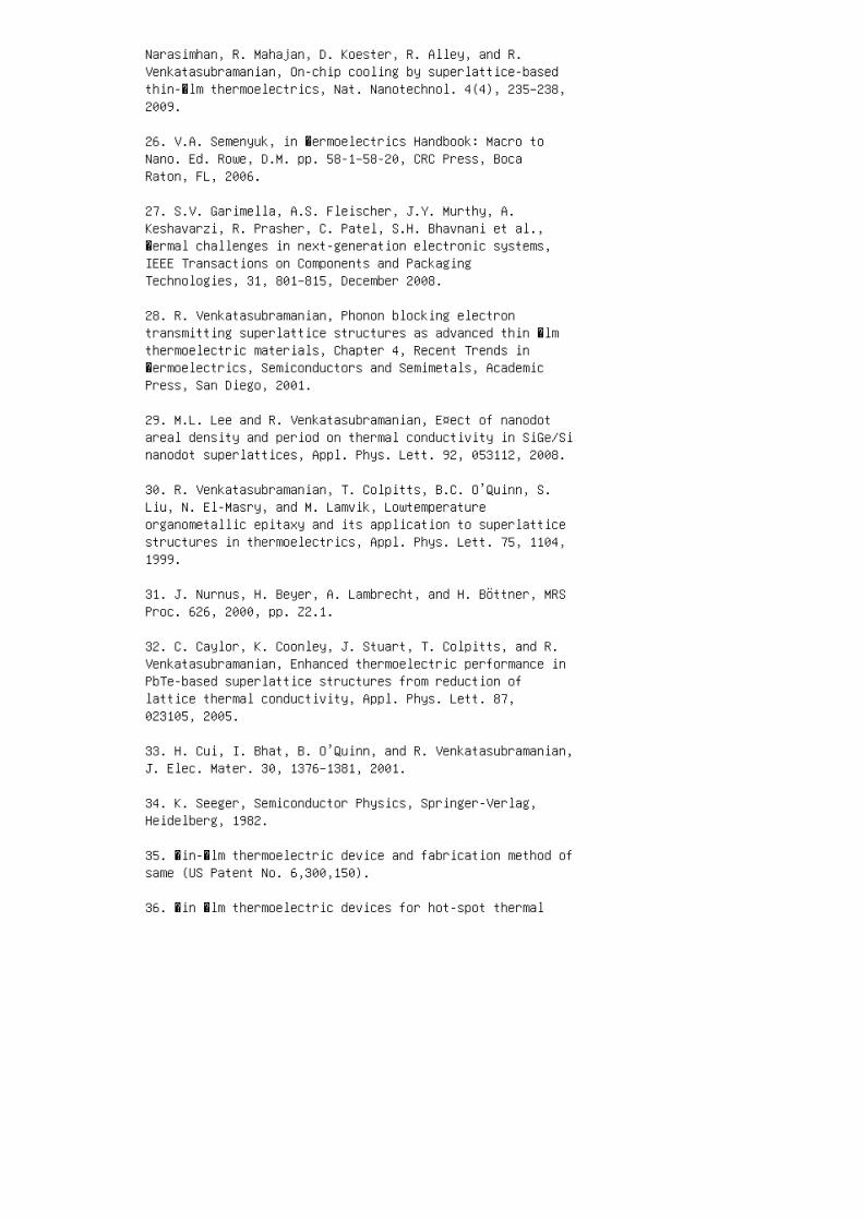
Narasimhan, R. Mahajan, D. Koester, R. Alley, and R.Venkatasubramanian, On-chip cooling by superlattice-basedthin-�lm thermoelectrics, Nat. Nanotechnol. 4(4), 235–238,2009.
26. V.A. Semenyuk, in �ermoelectrics Handbook: Macro toNano. Ed. Rowe, D.M. pp. 58-1–58-20, CRC Press, BocaRaton, FL, 2006.
27. S.V. Garimella, A.S. Fleischer, J.Y. Murthy, A.Keshavarzi, R. Prasher, C. Patel, S.H. Bhavnani et al.,�ermal challenges in next-generation electronic systems,IEEE Transactions on Components and PackagingTechnologies, 31, 801–815, December 2008.
28. R. Venkatasubramanian, Phonon blocking electrontransmitting superlattice structures as advanced thin �lmthermoelectric materials, Chapter 4, Recent Trends in�ermoelectrics, Semiconductors and Semimetals, AcademicPress, San Diego, 2001.
29. M.L. Lee and R. Venkatasubramanian, E¤ect of nanodotareal density and period on thermal conductivity in SiGe/Sinanodot superlattices, Appl. Phys. Lett. 92, 053112, 2008.
30. R. Venkatasubramanian, T. Colpitts, B.C. O’Quinn, S.Liu, N. El-Masry, and M. Lamvik, Lowtemperatureorganometallic epitaxy and its application to superlatticestructures in thermoelectrics, Appl. Phys. Lett. 75, 1104,1999.
31. J. Nurnus, H. Beyer, A. Lambrecht, and H. Böttner, MRSProc. 626, 2000, pp. Z2.1.
32. C. Caylor, K. Coonley, J. Stuart, T. Colpitts, and R.Venkatasubramanian, Enhanced thermoelectric performance inPbTe-based superlattice structures from reduction oflattice thermal conductivity, Appl. Phys. Lett. 87,023105, 2005.
33. H. Cui, I. Bhat, B. O’Quinn, and R. Venkatasubramanian,J. Elec. Mater. 30, 1376–1381, 2001.
34. K. Seeger, Semiconductor Physics, Springer-Verlag,Heidelberg, 1982.
35. �in-�lm thermoelectric device and fabrication method ofsame (US Patent No. 6,300,150).
36. �in �lm thermoelectric devices for hot-spot thermal
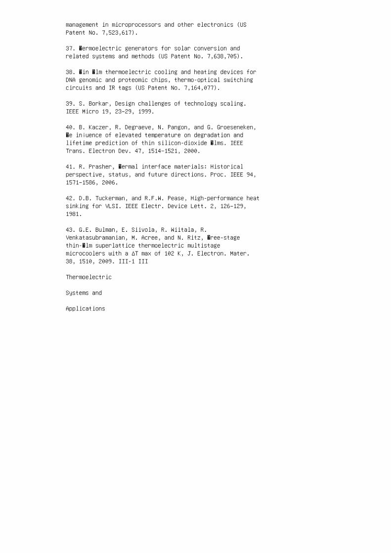
management in microprocessors and other electronics (USPatent No. 7,523,617).
37. �ermoelectric generators for solar conversion andrelated systems and methods (US Patent No. 7,638,705).
38. �in �lm thermoelectric cooling and heating devices forDNA genomic and proteomic chips, thermo-optical switchingcircuits and IR tags (US Patent No. 7,164,077).
39. S. Borkar, Design challenges of technology scaling.IEEE Micro 19, 23–29, 1999.
40. B. Kaczer, R. Degraeve, N. Pangon, and G. Groeseneken,�e in¡uence of elevated temperature on degradation andlifetime prediction of thin silicon-dioxide �lms. IEEETrans. Electron Dev. 47, 1514–1521, 2000.
41. R. Prasher, �ermal interface materials: Historicalperspective, status, and future directions. Proc. IEEE 94,1571–1586, 2006.
42. D.B. Tuckerman, and R.F.W. Pease, High-performance heatsinking for VLSI. IEEE Electr. Device Lett. 2, 126–129,1981.
43. G.E. Bulman, E. Siivola, R. Wiitala, R.Venkatasubramanian, M. Acree, and N. Ritz, �ree-stagethin-�lm superlattice thermoelectric multistagemicrocoolers with a ΔT max of 102 K, J. Electron. Mater.38, 1510, 2009. III-1 III
Thermoelectric
Systems and
Applications
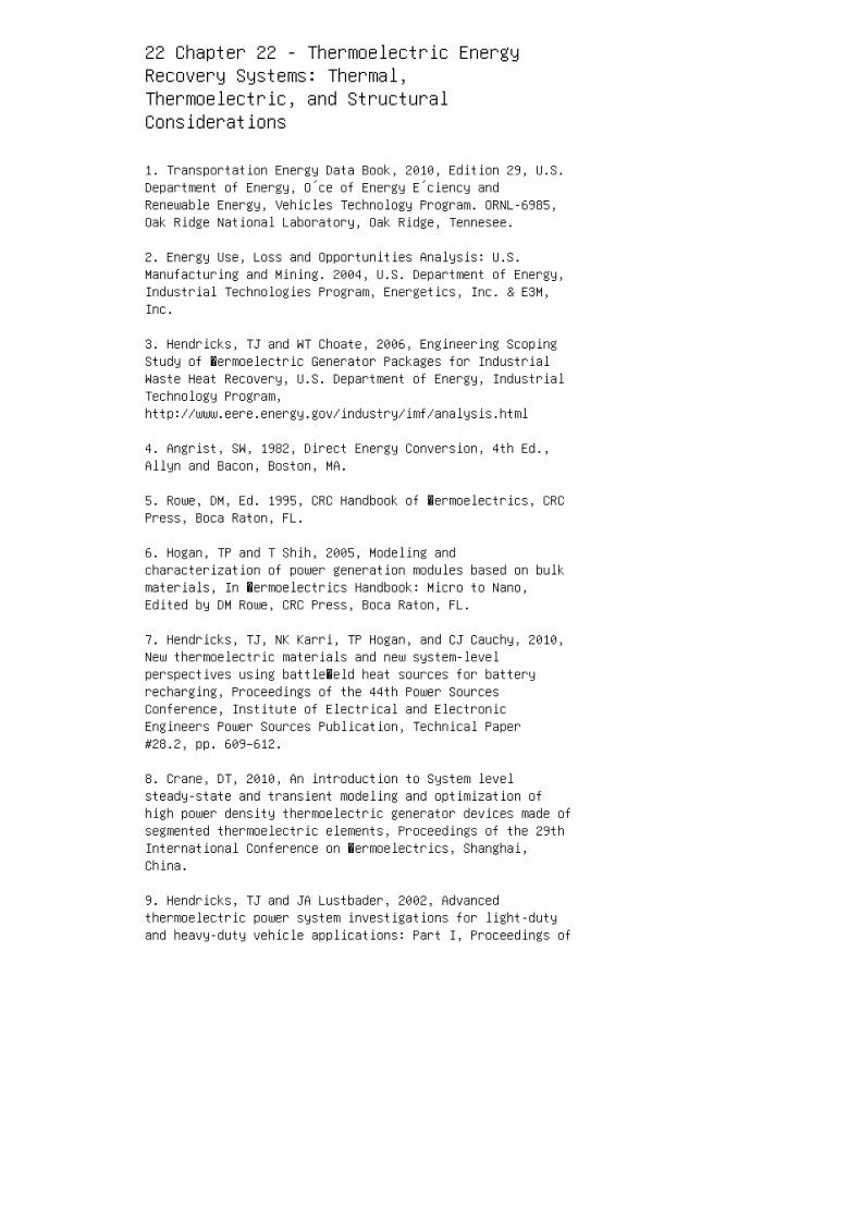
22 Chapter 22 - Thermoelectric EnergyRecovery Systems: Thermal,Thermoelectric, and StructuralConsiderations
1. Transportation Energy Data Book, 2010, Edition 29, U.S.Department of Energy, O´ce of Energy E´ciency andRenewable Energy, Vehicles Technology Program. ORNL-6985,Oak Ridge National Laboratory, Oak Ridge, Tennesee.
2. Energy Use, Loss and Opportunities Analysis: U.S.Manufacturing and Mining. 2004, U.S. Department of Energy,Industrial Technologies Program, Energetics, Inc. & E3M,Inc.
3. Hendricks, TJ and WT Choate, 2006, Engineering ScopingStudy of �ermoelectric Generator Packages for IndustrialWaste Heat Recovery, U.S. Department of Energy, IndustrialTechnology Program,http://www.eere.energy.gov/industry/imf/analysis.html
4. Angrist, SW, 1982, Direct Energy Conversion, 4th Ed.,Allyn and Bacon, Boston, MA.
5. Rowe, DM, Ed. 1995, CRC Handbook of �ermoelectrics, CRCPress, Boca Raton, FL.
6. Hogan, TP and T Shih, 2005, Modeling andcharacterization of power generation modules based on bulkmaterials, In �ermoelectrics Handbook: Micro to Nano,Edited by DM Rowe, CRC Press, Boca Raton, FL.
7. Hendricks, TJ, NK Karri, TP Hogan, and CJ Cauchy, 2010,New thermoelectric materials and new system-levelperspectives using battle�eld heat sources for batteryrecharging, Proceedings of the 44th Power SourcesConference, Institute of Electrical and ElectronicEngineers Power Sources Publication, Technical Paper#28.2, pp. 609–612.
8. Crane, DT, 2010, An introduction to System levelsteady-state and transient modeling and optimization ofhigh power density thermoelectric generator devices made ofsegmented thermoelectric elements, Proceedings of the 29thInternational Conference on �ermoelectrics, Shanghai,China.
9. Hendricks, TJ and JA Lustbader, 2002, Advancedthermoelectric power system investigations for light-dutyand heavy-duty vehicle applications: Part I, Proceedings of
the 21st International Conference on �ermoelectrics, LongBeach, CA, IEEE Catalogue #02TH8657, pp. 381–386.
10. Hendricks, TJ and JA Lustbader, 2002, Advancedthermoelectric power system investigations for light-dutyand heavy-duty vehicle applications: Part II, Proceedingsof the 21st International Conference on �ermoelectrics,Long Beach, CA, IEEE Catalogue #02TH8657, pp. 387–394.
11. Cobble, MH, 1995, Calculations of generatorperformance, CRC Handbook of �ermoelectrics, CRC Press,Boca Raton, FL.
12. Skrabek, EA and DS Trimmer, 1995, Properties of thegeneral TAGS system, In CRC Handbook of �ermoelectrics,ed. DM Rowe, CRC Press LLC, Boca Raton, FL, pp. 267–275.
13. Dughaish, ZH, 2002, Lead telluride as a thermoelectricmaterial for thermoelectric power generation, Physica B322: 205–223.
14. Swanson, BW, EV Somers, and RR Heikes, 1961.Optimization of a sandwiched TE device, Journal of HeatTransfer, 83: 77–82.
15. Crane, DT, 2003, Optimizing �ermoelectric Waste HeatRecovery from an Automotive Cooling System, PhDDissertation, University of Maryland, College Park, CollegePark, MD.
16. Crane, DT and LE Bell, 2006, Progress towardsmaximizing the performance of a thermoelectric powergenerator, Proceedings of the 25th International Conferenceon �ermoelectrics, Vienna, Austria: IEEE, pp. 11–16.
17. Crane, DT and LE Bell, 2009, Design to maximizeperformance of a thermoelectric power generator with adynamic thermal power source, Journal of Energy ResourcesTechnology, 131: 012401-1–8.
18. Crane, DT and GS Jackson, 2004, Optimization of cross¡ow heat exchangers for thermoelectric waste heatrecovery, International Journal of Energy Conversion andManagement, 45(9–10): 1565–1582.
19. Sherman, B, RR Heikes, and RW Ure Jr., 1960,Calculations of e´ciency of TE devices, Journal of AppliedPhysics, 31(1): 1–16.
20. Domenicali, CA, 1953, Irreversible thermodynamics of TE
e¤ects in inhomogeneous, anisotropic media, PhysicsReviews 92(4): 877–881.
21. Mahan, GD, 1991. Inhomogeneous TEs, Journal of AppliedPhysics 70(8): 4551.
22. Antonova, EE and DC Looman, 2005, Finite elements forthermoelectric device analysis in ANSYS, Proceedings of2005 24th International Conference on �ermoelectrics, pp.215–218.
23. Crane, DT, JW LaGrandeur, and LE Bell, 2010, Progressreport on BSST Led, U.S. DOE automotive waste heatrecovery program, Journal of Electronic Materials, 39(9):2142–2148.
24. Hendricks, TJ and NK Karri, 2009, Micro- andnano-technology: A critical design key in advancedthermoelectric cooling systems, Journal of ElectronicMaterials, 38(7): 1257–1267, DOI: 10.1007/s11664–009–0709–3, Springer Publishing, New York.
25. Hendricks, TJ, 2008, Microtechnology—A key to systemminiaturization in advanced energy recovery and conversionsystems, Proceedings of American Society of MechanicalEngineers 2nd International Conference on EnergySustainability, Jacksonville, FL, Paper # ES2008–54244.
26. Hendricks, TJ, 2006, Microchannel & minichannel heatexchangers in advanced energy recovery & conversionsystems, Proceedings of the ASME 2006 InternationalMechanical Engineering Congress and Exposition, IMECE2006– Advanced Energy System Division,American Society ofMechanical Engineers, New York, Paper # IMECE2006-14594.
27. Kays, WM and AL London, 1984, Compact Heat Exchangers,3rd Edition, McGraw-Hill, New York.
28. Incropera, FP and DP Dewitt, 1990, Fundamentals of Heatand Mass Transfer, 3rd Edition, Wiley & Sons, New York.
29. Liao, SM and Zhao, TS, 2002, Measurements of heattransfer coe´cients from supercritical carbon dioxide¡owing in horizontal mini/micro channels, Journal of HeatTransfer, Transactions of the ASME, 124, 413–420.
30. Hendricks, TJ, TP Hogan, ED Case, CJ Cauchy, NK Karri,J D’Angelo, C-I Wu, AQ Morrison, and F Ren, 2009, Advancedsoldier-based thermoelectric power systems using battle�eldheat sources, Energy Harvesting–From Fundamentals to
Devices, Edited by H Radousky, J Holbery, L Lewis, and FSchmidt (Mater. Res. Soc. Symp. Proc. Volume 1218E,Warrendale, PA, 2010), Paper ID # 1218-Z07-02.(Proceedings of the Materials Research Society 2009 FallMeeting, Symposium Z, Paper ID # 1218-Z07-02, Boston, MA,2009.)
31. Wang, Y and JD Holladay, 2005. Microreactor Technologyand Process Intensi¹cation, ACS Symposium Series 914,American Chemical Society, Oxford University Press.
32. Hall, BD, JL Micklash, JR Johnson, TP Hogan, and EDCase, 2007. A review of mechanical properties forthermoelectric materials, Materials Science and Technology2007 Conference, Detroit, Michigan.
23 Chapter 23 - Thermoelectric Harvestingof Low-Temperature Heat
1. D.M. Rowe, Commissioned IEE Review paper 81265,�ermoelectric power generation, Proceedings of the IEEE,Vol. 125, No. 11R, pp. 1113–1136, Nov 1978.
2. D.M. Rowe and C.M. Bhandari, Modern �ermoelectrics.Holt, Rinehart and Winston Ltd, London, England. ISBN0-03-91443-8, 1983.
3. D.M. Rowe, Proc 8th International Conference on�ermoelectric Energy Conversion, Nancy, France, pp.133–142, 10–13 July, 1989.
4. D.M. Rowe, S.K. Williams, A. Kaliazin, and G. Min, Proc4th European Conference on �ermolectrics, Madrid, pp.153–157, 1999.
5. S.G.K. Williams, D.M. Rowe, A. Kaliazin, and G. Min,Proc. 5th European Workshop on �ermoelectrics, Pardubice,Czech Republic, Sept. 1999.
6. Wikipedia, Solar Energy.
7. E. Weston, U.S. Patent No. 389,124, 1888.
8. E. Weston, E., U.S. Patent No 389,125, 1888.
9. W.W. Coblentz, Scienti¹c American, 127, 324, 1922.
10. M. Telkes, Solar thermoelectric generators, J. Appl.Phys, 25,765–777, 1954.
11. P.S. Castro and W. Happ, Performance of athermoelectric converter under constant heat ¡ux operation,J. Appl. Phys. 31,1314, 1960.
12. N. Fuschillo, R. Gibson, F.K. Eggleston, and J.Epstein, Flat plate thermoelectric solar cells,manufacturing process and life testing, Adv. Energy Cons.6,103. 1966.
13. V. Raag, L. Hankins, and M. Swerdling. Proceedings 2ndITC University of Texas, Arlington 22 March, pp. 60–7,1978.
14. D.M. Rowe, A high performance solar poweredthermoelectric generator, Appl. Energy 8, 269–273, 1981.
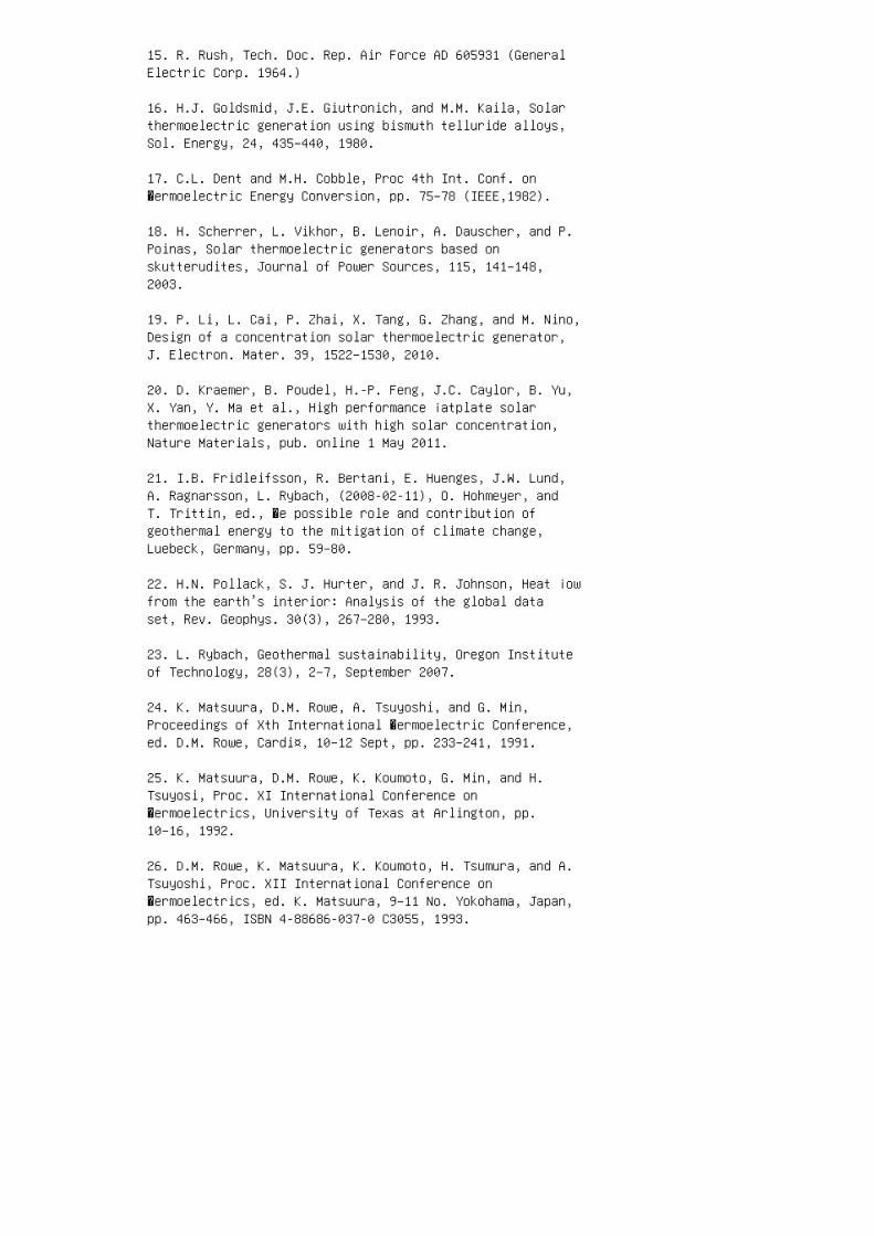
15. R. Rush, Tech. Doc. Rep. Air Force AD 605931 (GeneralElectric Corp. 1964.)
16. H.J. Goldsmid, J.E. Giutronich, and M.M. Kaila, Solarthermoelectric generation using bismuth telluride alloys,Sol. Energy, 24, 435–440, 1980.
17. C.L. Dent and M.H. Cobble, Proc 4th Int. Conf. on�ermoelectric Energy Conversion, pp. 75–78 (IEEE,1982).
18. H. Scherrer, L. Vikhor, B. Lenoir, A. Dauscher, and P.Poinas, Solar thermoelectric generators based onskutterudites, Journal of Power Sources, 115, 141–148,2003.
19. P. Li, L. Cai, P. Zhai, X. Tang, G. Zhang, and M. Nino,Design of a concentration solar thermoelectric generator,J. Electron. Mater. 39, 1522–1530, 2010.
20. D. Kraemer, B. Poudel, H.-P. Feng, J.C. Caylor, B. Yu,X. Yan, Y. Ma et al., High performance ¡atplate solarthermoelectric generators with high solar concentration,Nature Materials, pub. online 1 May 2011.
21. I.B. Fridleifsson, R. Bertani, E. Huenges, J.W. Lund,A. Ragnarsson, L. Rybach, (2008-02-11), O. Hohmeyer, andT. Trittin, ed., �e possible role and contribution ofgeothermal energy to the mitigation of climate change,Luebeck, Germany, pp. 59–80.
22. H.N. Pollack, S. J. Hurter, and J. R. Johnson, Heat ¡owfrom the earth’s interior: Analysis of the global dataset, Rev. Geophys. 30(3), 267–280, 1993.
23. L. Rybach, Geothermal sustainability, Oregon Instituteof Technology, 28(3), 2–7, September 2007.
24. K. Matsuura, D.M. Rowe, A. Tsuyoshi, and G. Min,Proceedings of Xth International �ermoelectric Conference,ed. D.M. Rowe, Cardi¤, 10–12 Sept, pp. 233–241, 1991.
25. K. Matsuura, D.M. Rowe, K. Koumoto, G. Min, and H.Tsuyosi, Proc. XI International Conference on�ermoelectrics, University of Texas at Arlington, pp.10–16, 1992.
26. D.M. Rowe, K. Matsuura, K. Koumoto, H. Tsumura, and A.Tsuyoshi, Proc. XII International Conference on�ermoelectrics, ed. K. Matsuura, 9–11 No. Yokohama, Japan,pp. 463–466, ISBN 4-88686-037-0 C3055, 1993.
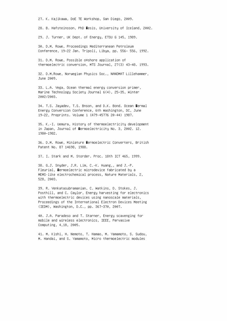
27. K. Kajikawa, DoE TE Workshop, San Diego, 2009.
28. B. Hafsteinsson, PhD �esis, University of Iceland, 2002.
29. J. Turner, UK Dept. of Energy, ETSU G 145, 1989.
30. D.M. Rowe, Proceedings Mediterranean PetroleumConference, 19–22 Jan. Tripoli, Libya, pp. 556– 556, 1992.
31. D.M. Rowe, Possible o¤shore application ofthermoelectric conversion, MTS Journal, 27(3) 43–48. 1993.
32. D.M.Rowe, Norwegian Physics Soc., NANOMAT Lillehammer,June 2009.
33. L.A. Vega, Ocean thermal energy conversion primer,Marine Technology Society Journal 6(4), 25–35, Winter2002/2003.
34. T.S. Jayadev, T.S. Bnson, and D.K. Bond. Ocean �ermalEnergy Conversion Conference, 6th Washington, DC, June19–22, Preprints. Volume 1 (A79-45776 20-44) 1987.
35. K.-I. Uemura, History of thermoelectricity developmentin Japan, Journal of �ermoelectricity No. 3, 2002. 12.1980–1982.
36. D.M. Rowe, Miniature �ermoelectric Converters, BritishPatent No. 87 14698, 1988.
37. I. Stark and M. Storder. Proc. 18th ICT 465, 1999.
38. G.J. Snyder, J.R. Lim, C.-K. Huang,, and J.-P.Fleurial, �ermoelectric microdevice fabricated by aMEMS-like electrochemical process, Nature Materials, 2,528, 2003.
39. R. Venkatasubramanian, C. Watkins, D. Stokes, J.Posthill, and C. Caylor, Energy harvesting for electronicswith thermoelectric devices using nanoscale materials,Proceedings of the International Electron Devices Meeting(IEDM), Washington, D.C., pp. 367–370, 2007.
40. J.A. Paradeso and T. Starner, Energy scavenging formobile and wireless electronics, IEEE, PervasiveComputing, 4,18, 2005.
41. M. Kishi, H. Nemoto, T. Hamao, M. Yamamoto, S. Sudou,M. Handai, and S. Yamamoto, Micro thermoelectric modules
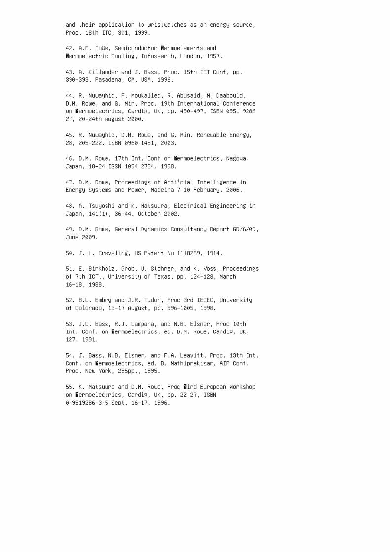
and their application to wristwatches as an energy source,Proc. 18th ITC, 301, 1999.
42. A.F. Io¤e, Semiconductor �ermoelements and�ermoelectric Cooling, Infosearch, London, 1957.
43. A. Killander and J. Bass, Proc. 15th ICT Conf, pp.390–393, Pasadena, CA, USA, 1996.
44. R. Nuwayhid, F. Moukalled, R. Abusaid, M, Daabould,D.M. Rowe, and G. Min, Proc. 19th International Conferenceon �ermoelectrics, Cardi¤, UK, pp. 490–497, ISBN 0951 928627, 20–24th August 2000.
45. R. Nuwayhid, D.M. Rowe, and G. Min. Renewable Energy,28, 205–222. ISBN 0960-1481, 2003.
46. D.M. Rowe. 17th Int. Conf on �ermoelectrics, Nagoya,Japan, 18–24 ISSN 1094 2734, 1998.
47. D.M. Rowe, Proceedings of Arti¹cial Intelligence inEnergy Systems and Power, Madeira 7–10 February, 2006.
48. A. Tsuyoshi and K. Matsuura, Electrical Engineering inJapan, 141(1), 36–44. October 2002.
49. D.M. Rowe, General Dynamics Consultancy Report GD/6/09,June 2009.
50. J. L. Creveling, US Patent No 1118269, 1914.
51. E. Birkholz, Grob, U. Stohrer, and K. Voss, Proceedingsof 7th ICT., University of Texas, pp. 124–128, March16–18, 1988.
52. B.L. Embry and J.R. Tudor, Proc 3rd IECEC, Universityof Colorado, 13–17 August, pp. 996–1005, 1998.
53. J.C. Bass, R.J. Campana, and N.B. Elsner, Proc 10thInt. Conf. on �ermoelectrics, ed. D.M. Rowe, Cardi¤, UK,127, 1991.
54. J. Bass, N.B. Elsner, and F.A. Leavitt, Proc. 13th Int.Conf. on �ermoelectrics, ed. B. Mathiprakisam, AIP Conf.Proc, New York, 295pp., 1995.
55. K. Matsuura and D.M. Rowe, Proc �ird European Workshopon �ermoelectrics, Cardi¤, UK, pp. 22–27, ISBN0-9519286-3-5 Sept. 16–17, 1996.
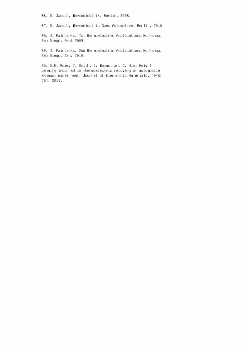
56. D. Jansch, �ermoelektrik, Berlin, 2008.
57. D. Jansch, �ermoelectric Goes Automotive, Berlin, 2010.
58. J. Fairbanks, Ist �ermoelectric Applications Workshop,San Diego, Sept 2009.
59. J. Fairbanks, 2nd �ermoelectric Applications Workshop,San Diego, Jan. 2010.
60. D.M. Rowe, J. Smith, G. �omas, and G. Min, Weightpenalty incurred in thermoelectric recovery of automobileexhaust waste heat, Journal of Electronic Materials, 40(5),784, 2011.
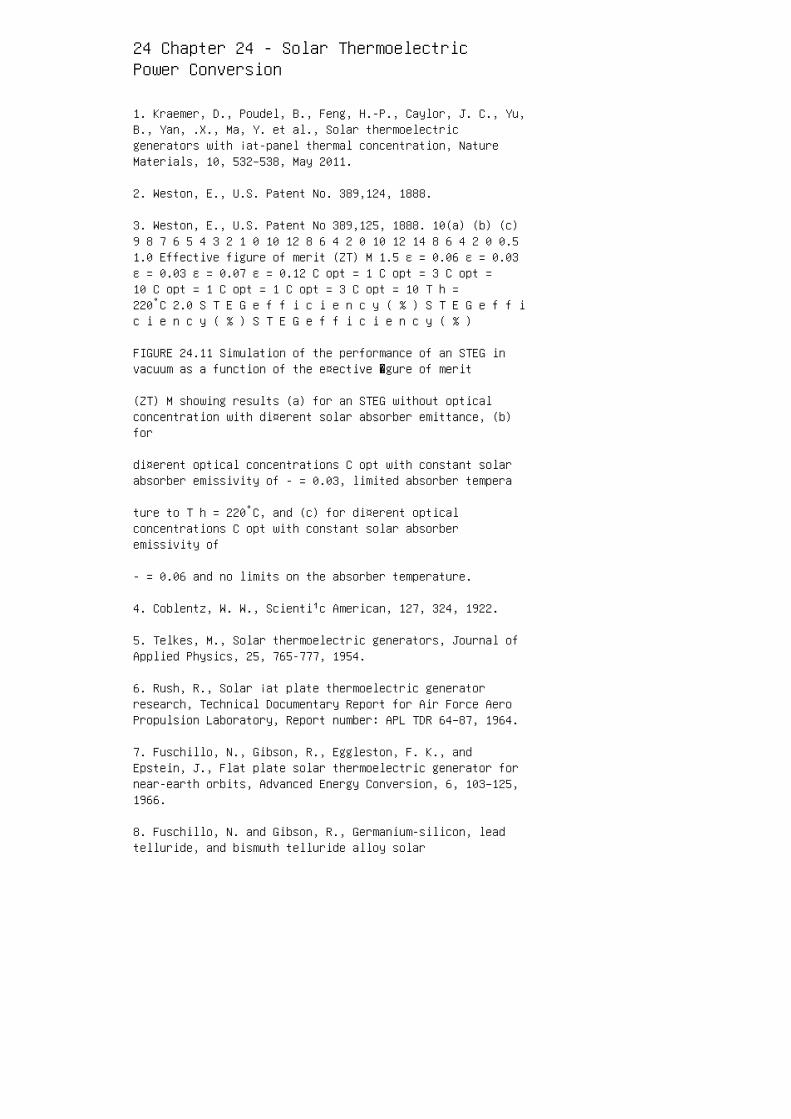
24 Chapter 24 - Solar ThermoelectricPower Conversion
1. Kraemer, D., Poudel, B., Feng, H.-P., Caylor, J. C., Yu,B., Yan, .X., Ma, Y. et al., Solar thermoelectricgenerators with ¡at-panel thermal concentration, NatureMaterials, 10, 532–538, May 2011.
2. Weston, E., U.S. Patent No. 389,124, 1888.
3. Weston, E., U.S. Patent No 389,125, 1888. 10(a) (b) (c)9 8 7 6 5 4 3 2 1 0 10 12 8 6 4 2 0 10 12 14 8 6 4 2 0 0.51.0 Effective figure of merit (ZT) M 1.5 ε = 0.06 ε = 0.03ε = 0.03 ε = 0.07 ε = 0.12 C opt = 1 C opt = 3 C opt =10 C opt = 1 C opt = 1 C opt = 3 C opt = 10 T h =220°C 2.0 S T E G e f f i c i e n c y ( % ) S T E G e f f ic i e n c y ( % ) S T E G e f f i c i e n c y ( % )
FIGURE 24.11 Simulation of the performance of an STEG invacuum as a function of the e¤ective �gure of merit
(ZT) M showing results (a) for an STEG without opticalconcentration with di¤erent solar absorber emittance, (b)for
di¤erent optical concentrations C opt with constant solarabsorber emissivity of - = 0.03, limited absorber tempera
ture to T h = 220°C, and (c) for di¤erent opticalconcentrations C opt with constant solar absorberemissivity of
- = 0.06 and no limits on the absorber temperature.
4. Coblentz, W. W., Scienti¹c American, 127, 324, 1922.
5. Telkes, M., Solar thermoelectric generators, Journal ofApplied Physics, 25, 765-777, 1954.
6. Rush, R., Solar ¡at plate thermoelectric generatorresearch, Technical Documentary Report for Air Force AeroPropulsion Laboratory, Report number: APL TDR 64–87, 1964.
7. Fuschillo, N., Gibson, R., Eggleston, F. K., andEpstein, J., Flat plate solar thermoelectric generator fornear-earth orbits, Advanced Energy Conversion, 6, 103–125,1966.
8. Fuschillo, N. and Gibson, R., Germanium-silicon, leadtelluride, and bismuth telluride alloy solar
thermoelectric generators for venus and mercury probes,Advanced Energy Conversion, 7, 43–52, 1967.
9. Raag, V., Berlin, R. E., and Bifano, W. J., Flat platethermoelectric generators for solar-probe missions,Intersociety Energy Conversion Engineering Conference,Boulder, CO, 1968.
10. Scherrer, H., Vikhor, L., Lenoir, B., Dauscher, A.,Poinas, and P., Solar thermoelectric generator based onskutterudites, Journal of Power Sources, 115, 141–148,2003.
11. Dent, C. L. and Cobble, M. H., A solar thermoelectricgenerator experiment and analysis, Proceedings of 4th ICT,pp. 75–78, 1982.
12. Omer, S. A. and In�eld, D. G., Design optimization ofthermoelectric devices for solar power generation, SolarEnergy Materials and Solar Cells, 53, 67–82, 1998.
13. Amatya, R. and Ram, R. J., Solar thermoelectricgenerator for micropower applications, Journal ofElectronic Materials, 39, 1735–1740, 2010.
14. Li, P., Cai, L., Zhai, P., Tang, X., Zhang, Q., andNiino, M., Design of a concentration solar thermoelectricgenerator, Journal of Electronic Materials, 39, 1522–1530,2010.
15. Price, H., Assessment of Parabolic Trough and PowerTower Solar Technology Cost and Performance Forecasts,NREL/SR-550-34440, 2003.
16. Caillat, T., Fleurial, J.-P., and Snyder, G. J.,Development of high e´ciency segmented thermoelectricunicouples, ICT, 2001.
17. McEnaney, K., Kraemer, D., Ren, Z. F., and Chen, G.,Modeling of concentrated solar thermoelectric generators,Journal of Applied Physics, 110, 074502, 2011.
18. Goldsmid, H. J., Giutronich, J. E., and Kaila M. M.,Solar thermoelectric generation using bismuth telluridealloy, Solar Energy, 22, 435–440, 1980.
19. Vatcharasathien, N., Hirunlabh, J., Khedari, J., andDaguenet, M., Design and analysis of solar thermoelectricpower generation system, Journal of Sustainable Energy,24:3, 115–127, 2005.
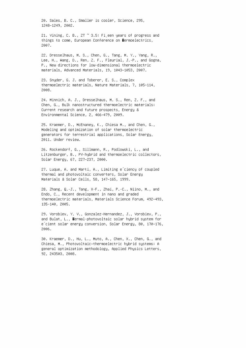
20. Sales, B. C., Smaller is cooler, Science, 295,1248–1249, 2002.
21. Vining, C. B., ZT ~ 3.5: Fi¸een years of progress andthings to come, European Conference on �ermoelectrics,2007.
22. Dresselhaus, M. S., Chen, G., Tang, M. Y., Yang, R.,Lee, H., Wang, D., Ren, Z. F., Fleurial, J.-P., and Gogna,P., New directions for low-dimensional thermoelectricmaterials, Advanced Materials, 19, 1043–1053, 2007.
23. Snyder, G. J. and Toberer, E. S., Complexthermoelectric materials, Nature Materials, 7, 105–114,2008.
24. Minnich, A. J., Dresselhaus, M. S., Ren, Z. F., andChen, G., Bulk nanostructured thermoelectric materials:Current research and future prospects, Energy &Environmental Science, 2, 466–479, 2009.
25. Kraemer, D., McEnaney, K., Chiesa M., and Chen, G.,Modeling and optimization of solar thermoelectricgenerators for terrestrial applications, Solar Energy,2011. Under review.
26. Rockendorf, G., Sillmann, R., Podlowski, L., andLitzenburger, B., PV-hybrid and thermoelectric collectors,Solar Energy, 67, 227–237, 2000.
27. Luque, A. and Marti, A., Limiting e´ciency of coupledthermal and photovoltaic converters, Solar EnergyMaterials & Solar Cells, 58, 147–165, 1999.
28. Zhang, Q.-J., Tang, X-F., Zhai, P.-C., Niino, M., andEndo, C., Recent development in nano and gradedthermoelectric materials, Materials Science Forum, 492–493,135–140, 2005.
29. Vorobiev, Y. V., Gonzalez-Hernandez, J., Vorobiev, P.,and Bulat, L., �ermal-photovoltaic solar hybrid system fore´cient solar energy conversion, Solar Energy, 80, 170–176,2006.
30. Kraemer, D., Hu, L., Muto, A., Chen, X., Chen, G., andChiesa, M., Photovoltaic–thermoelectric hybrid systems: Ageneral optimization methodology, Applied Physics Letters,92, 243503, 2008.
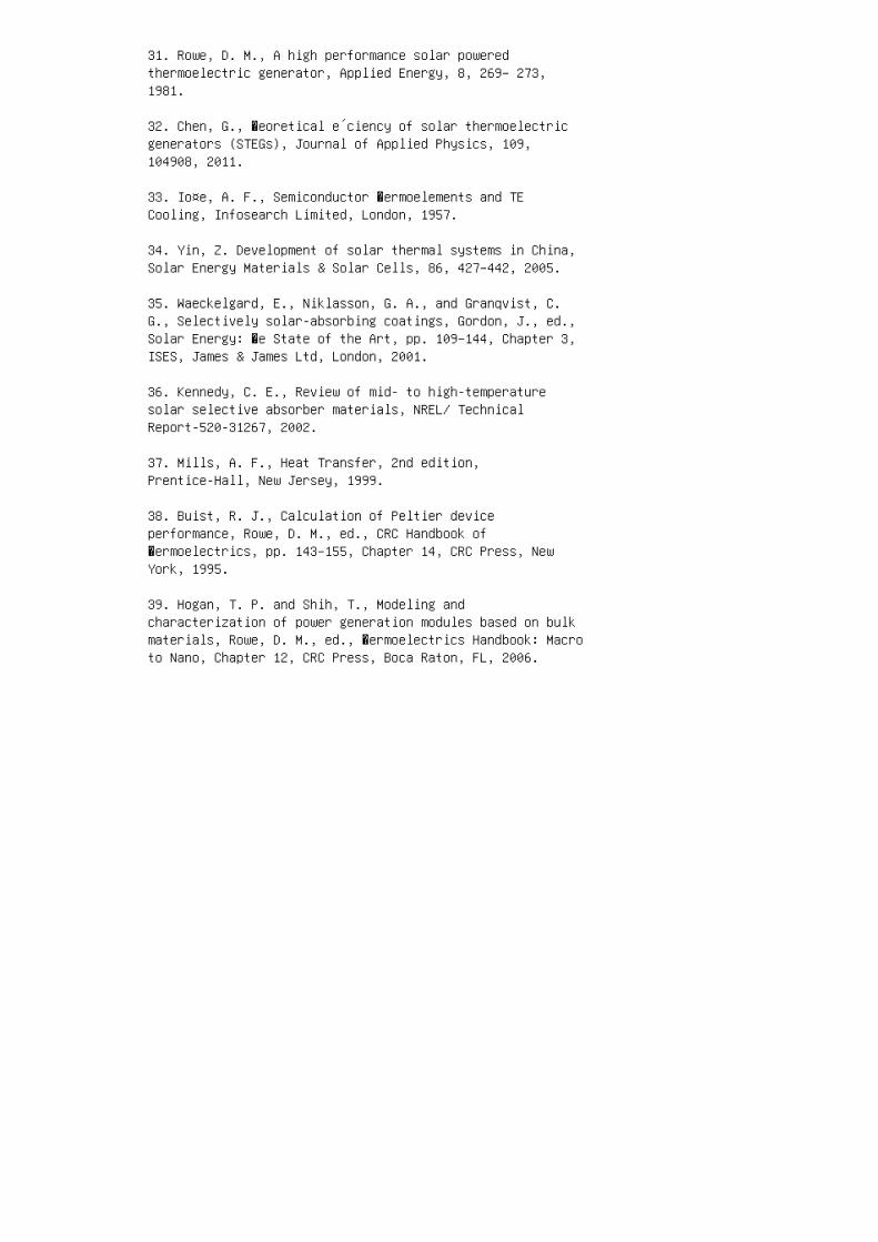
31. Rowe, D. M., A high performance solar poweredthermoelectric generator, Applied Energy, 8, 269– 273,1981.
32. Chen, G., �eoretical e´ciency of solar thermoelectricgenerators (STEGs), Journal of Applied Physics, 109,104908, 2011.
33. Io¤e, A. F., Semiconductor �ermoelements and TECooling, Infosearch Limited, London, 1957.
34. Yin, Z. Development of solar thermal systems in China,Solar Energy Materials & Solar Cells, 86, 427–442, 2005.
35. Waeckelgard, E., Niklasson, G. A., and Granqvist, C.G., Selectively solar-absorbing coatings, Gordon, J., ed.,Solar Energy: �e State of the Art, pp. 109–144, Chapter 3,ISES, James & James Ltd, London, 2001.
36. Kennedy, C. E., Review of mid- to high-temperaturesolar selective absorber materials, NREL/ TechnicalReport-520-31267, 2002.
37. Mills, A. F., Heat Transfer, 2nd edition,Prentice-Hall, New Jersey, 1999.
38. Buist, R. J., Calculation of Peltier deviceperformance, Rowe, D. M., ed., CRC Handbook of�ermoelectrics, pp. 143–155, Chapter 14, CRC Press, NewYork, 1995.
39. Hogan, T. P. and Shih, T., Modeling andcharacterization of power generation modules based on bulkmaterials, Rowe, D. M., ed., �ermoelectrics Handbook: Macroto Nano, Chapter 12, CRC Press, Boca Raton, FL, 2006.
25 Chapter 25 - Automotive Applicationsof Thermoelectric Materials
1. J. Yang, K. B. Ledbetter, and F. R. Stabler,�ermoelectric methods to control temperature of batteries,US Patent, US2006028182A1, Feb. 9, 2006.
2. J. Yang, M. Cai, and F. R. Stabler, �ermoelectriccatalytic converter temperature control, US Patent,US7,051,522 B2, May 30, 2006.
3. S. Pagerit, A. Rousseau, and P. Sharer, Fuel economysensitivity to vehicle mass for advanced vehiclepowertrains, SAE paper 2006-01-0665, SAE World Congress,Detroit, April 2006.
4. J. Yang, M. E. Matouka, and F. R. Stabler, Auxiliaryelectrical power generation, US Patent, US7,493,766, B2,Feb. 24, 2009.
5. A. F. Io¤e, Semiconductor �ermoelements and�ermoelectric Cooling, (Infosearch Limited, London, 1957).
7. T. M. Tritt and M. A. Subramanian, editors, Harvestingenergy through thermoelectrics: Power generation andcooling, MRS Bull. 31, 188–229, 2006.
8. M. S. El Genk, H. H. Saber, T. Caillat, and J. Sakamoto,Test results and performance comparisons of coated andUN-coated skutterudite-based segmented unicouples, J.Energy Cons. Manage. 47, 174, 2006.
9. R. W. Rice, Mechanical Properties of Ceramics andComposites (Marcel Dekker, New York, 2000).
10. Y. Gelbstein, G. Gotesman, Y. Lishzinker, Z. Dashevsky,and M. P. Dariel, Mechanical properties of PbTe-basedthermoelectric semiconductors, Scripta Mater. 58, 251,2008.
11. W. Brostow, K. P. Menard, and J. B. White,�ermomechanical characterization of bismuth telluridebased thermoelectric materials, Mat. Res. Soc. Symp. Proc.691, G13.3, 2002.
12. F. Ren, E. D. Case, E. J. Timm, M. D. Jacobs, and H. J.Schock, Weibull analysis of biaxial fracture strength ofcast p-type LAST-T thermoelectric material, Philos. Mag.Lett. 86, 673, 2006.
13. J. R. Salvador, J. Yang, X. Shi, H. Wang, and A.A.Wereszczak, Transport and mechanical property evaluationof (AgSbTe) 1-x (GeTe) x (x = 0.80, 0.82, 0.85, 0.87,0.90), J. Solid State Chem. 182, 2088, 2009.
14. A. L. Pilchak, F. Ren, E. D. Case, E. J. Timm, H. J.Schock, C. –I., Wu, and T. P. Hogan, Characterization ofdry milled powders of LAST (lead-antimony-silver-tellurium)thermoelectric material, Philos. Mag. 87, 4567, 2007.
15. N. I. Erzin and N. V. Makov, Appl. Sol. Energy 1, 33,1965.
16. H. J. Goldsmid, Electronic Refrigeration, (PionLimited, London, 1986), p. 165.
17. K. Matsubara, �e performance of a segmentedthermoelectric converter using Yb-based �lledskutterudites and Bi 2 Te 3 -based materials, Mat. Res.Soc. Symp. Proc. 691, 327, 2002.
18. L. Chen, J. Fan, S. Bai, and J. Yang, CoSb 3 -basedthermoelectric device fabrication method, US Patent,US7,321,157, B2, 2008.
19. D. T. Morelli, �ermoelectric devices, in Encyclopediaof Applied Physics, Vol. 21 (VCH, New York, 1997), pp.339–354.
20. T. M. Tritt, editor, Semiconductors and Semimetals,Vol. 69–71 (Academic Press, San Diego, 2001).
21. D. Hicks and M. S. Dresselhaus, E¤ect of quantum-wellstructures on the thermoelectric �gure of merit, Phys.Rev. B 47, 12727, 1993.
22. R. Venkatasubramanian, E. Siivola, T. Colpitts, and B.O’Quinn, �in-�lm thermoelectric devices with highroom-temperature �gures of merit, Nature 413, 597, 2001.
23. T. C. Harman, P. Taylor, M. P. Walsh, and B. E.Laforge, Quantum dot superlattice thermoelectric materialsand devices, Science 297, 2229, 2002.
24. T. C. Harman, M. P. Walsh, B. E. Laforge, and W. W.Turner, Nanostructured thermoelectric materials, J.Electron. Mater. 34, L19, 2005.
25. H. Ohta, S. W. Kim, Y. Mune, T. Mizoguchi, K. Nomura,S. Ohta, T. Nomura et al., Giant thermoelectric Seebeck
coe´cient of two-dimensional electron gas in SrTiO 3 , Nat.Mater. 6, 129, 2007.
26. K. F. Hsu, S. Loo, F. Guo, W. Chen, J. S. Dyck, C.Uher, T. Hogan, E. K. Polychroniadis, and M. G.Kanatzidis, Cubic AgPb m SbTe 2+m : Bulk thermoelectricmaterials with high �gure of merit, Science 303, 818,2004.
27. A. I. Hochbaum, R. Chen, R. D. Delgado, W. Liang, E. C.Garnett, M. Najarian, A. Majumdar, and P. Yang, Enhancedthermoelectric performance of rough silicon nanowires,Nature 451, 163, 2008.
28. A. I. Boukia, Y. Bunimovich, J. Tahir-Kheli, J.-K. Yu,W. A. Goddard III, and J. R. Heath, Silicon nanowires ase´cient thermoelectric materials, Nature 451, 168, 2008.
29. B. Poudel, Q. Hao, Y. Ma, Y. Lan, A. Minnich, B. Yu, X.Yan et al., High-thermoelectric performance ofnanostructured bismuth antimony telluride bulk alloys,Science 320, 634, 2008.
32. D. Y. Chung, T. Hogan, P. Brazis, M. Rocci-lane, C. R.Kannewurf, M. Bastea, C. Uher, and M. G. Kanatzidis, CsBi4 Te 6 : A high-performance thermoelectric material forlow-temperature applications, Science 287, 1024, 2000.
33. J. Yang, W. Zhang, S. Q. Bai, Z. Mei, and L. D. Chen,Dual-frequency resonant phonon scattering in Ba x R y Co 4Sb 12 (R = La, Ce, and Sr), Appl. Phys. Lett. 90, 192111,2007.
34. X. Shi, H. Kong, C. Uher, J. R. Salvador, J. Yang, andH. Wang, Low thermal conductivity and high thermoelectric�gure of merit in n-type Ba x Yb y Co 4 Sb 12 double-�lledskutterudites, Appl. Phys. Lett. 92, 182101, 2008.
35. X. Shi, Jiong Yang, J. R. Salvador, M. Chi, J. Cho, H.Wang, S. Bai, J. Yang, W. Zhang, and L. Chen,Multiple-�lled skutterudites: High thermoelectric �gure ofmerit through separately optimizing electrical and thermaltransports, J. Am. Chem. Soc. 133, 7837, 2011.
36. I. Terasaki, Y. Sasago, and K. Uchinokura, Largethermoelectric power in NaCo 2 O 4 single crystals, Phys.Rev. B 56, R12685, 1997.
37. K. Fujita, T. Mochida, and K. Nakamura,High-temperature thermoelectric properties of Na x CoO 2-δ
single crystals, Jpn. J. Appl. Phys. 40, 4644, 2001.
38. R. funahashi, I. Matsubara, H. Ikuta, T. Takeuchi, U.Mizutani, and S. Sodeoka, An oxide single crystal withhigh thermoelectric performance in air, Jpn. J. Appl. Phys.Pt. 2 39, L1127, 2000.
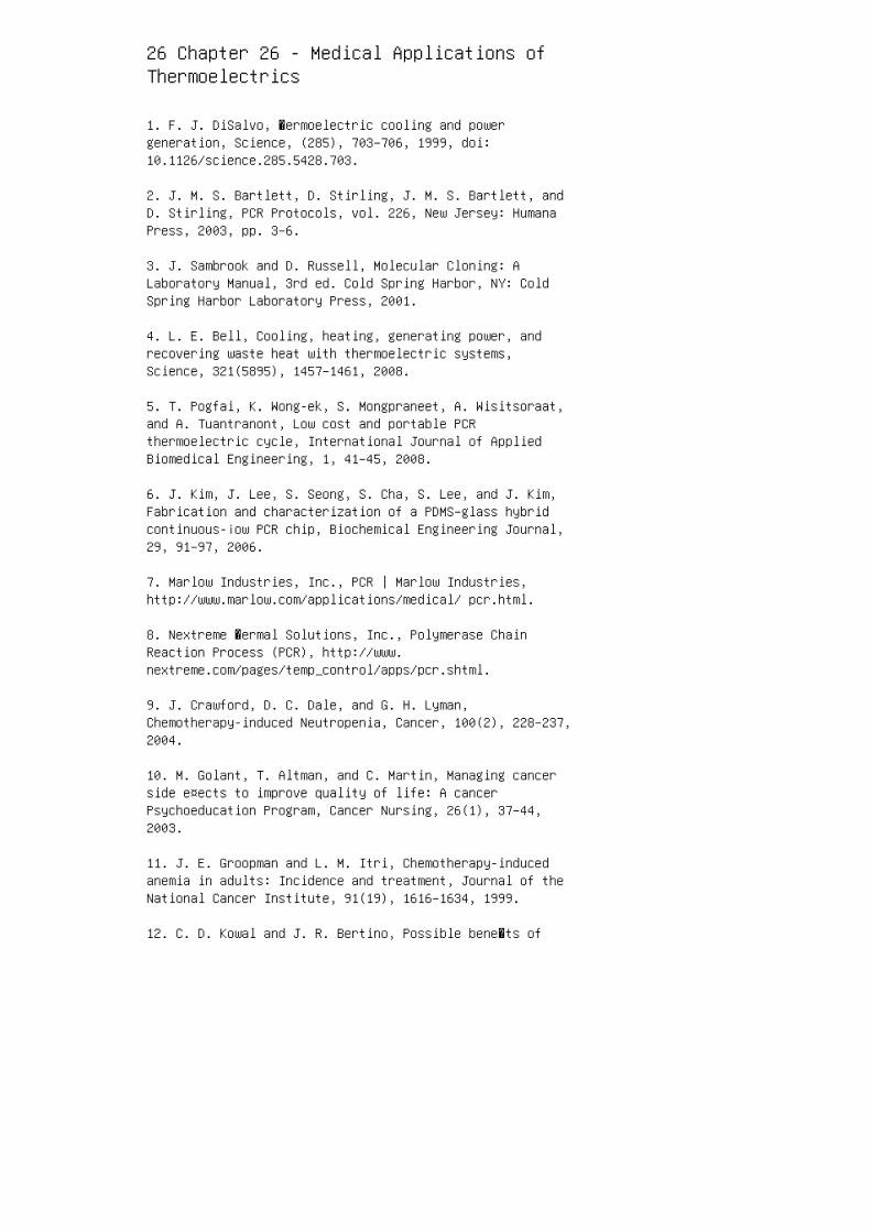
26 Chapter 26 - Medical Applications ofThermoelectrics
1. F. J. DiSalvo, �ermoelectric cooling and powergeneration, Science, (285), 703–706, 1999, doi:10.1126/science.285.5428.703.
2. J. M. S. Bartlett, D. Stirling, J. M. S. Bartlett, andD. Stirling, PCR Protocols, vol. 226, New Jersey: HumanaPress, 2003, pp. 3–6.
3. J. Sambrook and D. Russell, Molecular Cloning: ALaboratory Manual, 3rd ed. Cold Spring Harbor, NY: ColdSpring Harbor Laboratory Press, 2001.
4. L. E. Bell, Cooling, heating, generating power, andrecovering waste heat with thermoelectric systems,Science, 321(5895), 1457–1461, 2008.
5. T. Pogfai, K. Wong-ek, S. Mongpraneet, A. Wisitsoraat,and A. Tuantranont, Low cost and portable PCRthermoelectric cycle, International Journal of AppliedBiomedical Engineering, 1, 41–45, 2008.
6. J. Kim, J. Lee, S. Seong, S. Cha, S. Lee, and J. Kim,Fabrication and characterization of a PDMS–glass hybridcontinuous-¡ow PCR chip, Biochemical Engineering Journal,29, 91–97, 2006.
7. Marlow Industries, Inc., PCR | Marlow Industries,http://www.marlow.com/applications/medical/ pcr.html.
8. Nextreme �ermal Solutions, Inc., Polymerase ChainReaction Process (PCR), http://www.nextreme.com/pages/temp_control/apps/pcr.shtml.
9. J. Crawford, D. C. Dale, and G. H. Lyman,Chemotherapy-induced Neutropenia, Cancer, 100(2), 228–237,2004.
10. M. Golant, T. Altman, and C. Martin, Managing cancerside e¤ects to improve quality of life: A cancerPsychoeducation Program, Cancer Nursing, 26(1), 37–44,2003.
11. J. E. Groopman and L. M. Itri, Chemotherapy-inducedanemia in adults: Incidence and treatment, Journal of theNational Cancer Institute, 91(19), 1616–1634, 1999.
12. C. D. Kowal and J. R. Bertino, Possible bene�ts of
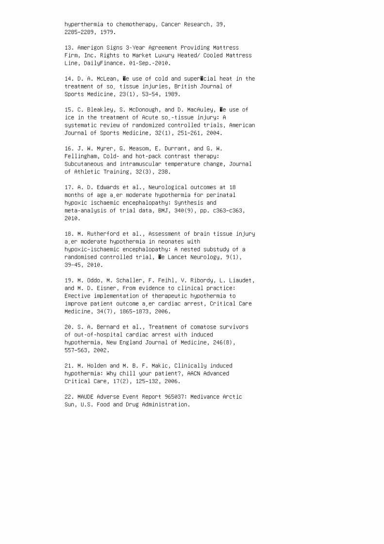
hyperthermia to chemotherapy, Cancer Research, 39,2285–2289, 1979.
13. Amerigon Signs 3-Year Agreement Providing MattressFirm, Inc. Rights to Market Luxury Heated/ Cooled MattressLine, DailyFinance. 01-Sep.-2010.
14. D. A. McLean, �e use of cold and super�cial heat in thetreatment of so¸ tissue injuries, British Journal ofSports Medicine, 23(1), 53–54, 1989.
15. C. Bleakley, S. McDonough, and D. MacAuley, �e use ofice in the treatment of Acute so¸-tissue injury: Asystematic review of randomized controlled trials, AmericanJournal of Sports Medicine, 32(1), 251–261, 2004.
16. J. W. Myrer, G. Measom, E. Durrant, and G. W.Fellingham, Cold- and hot-pack contrast therapy:Subcutaneous and intramuscular temperature change, Journalof Athletic Training, 32(3), 238.
17. A. D. Edwards et al., Neurological outcomes at 18months of age a¸er moderate hypothermia for perinatalhypoxic ischaemic encephalopathy: Synthesis andmeta-analysis of trial data, BMJ, 340(9), pp. c363–c363,2010.
18. M. Rutherford et al., Assessment of brain tissue injurya¸er moderate hypothermia in neonates withhypoxic–ischaemic encephalopathy: A nested substudy of arandomised controlled trial, �e Lancet Neurology, 9(1),39–45, 2010.
19. M. Oddo, M. Schaller, F. Feihl, V. Ribordy, L. Liaudet,and M. D. Eisner, From evidence to clinical practice:E¤ective implementation of therapeutic hypothermia toimprove patient outcome a¸er cardiac arrest, Critical CareMedicine, 34(7), 1865–1873, 2006.
20. S. A. Bernard et al., Treatment of comatose survivorsof out-of-hospital cardiac arrest with inducedhypothermia, New England Journal of Medicine, 246(8),557–563, 2002.
21. M. Holden and M. B. F. Makic, Clinically inducedhypothermia: Why chill your patient?, AACN AdvancedCritical Care, 17(2), 125–132, 2006.
22. MAUDE Adverse Event Report 965037: Medivance ArcticSun, U.S. Food and Drug Administration.
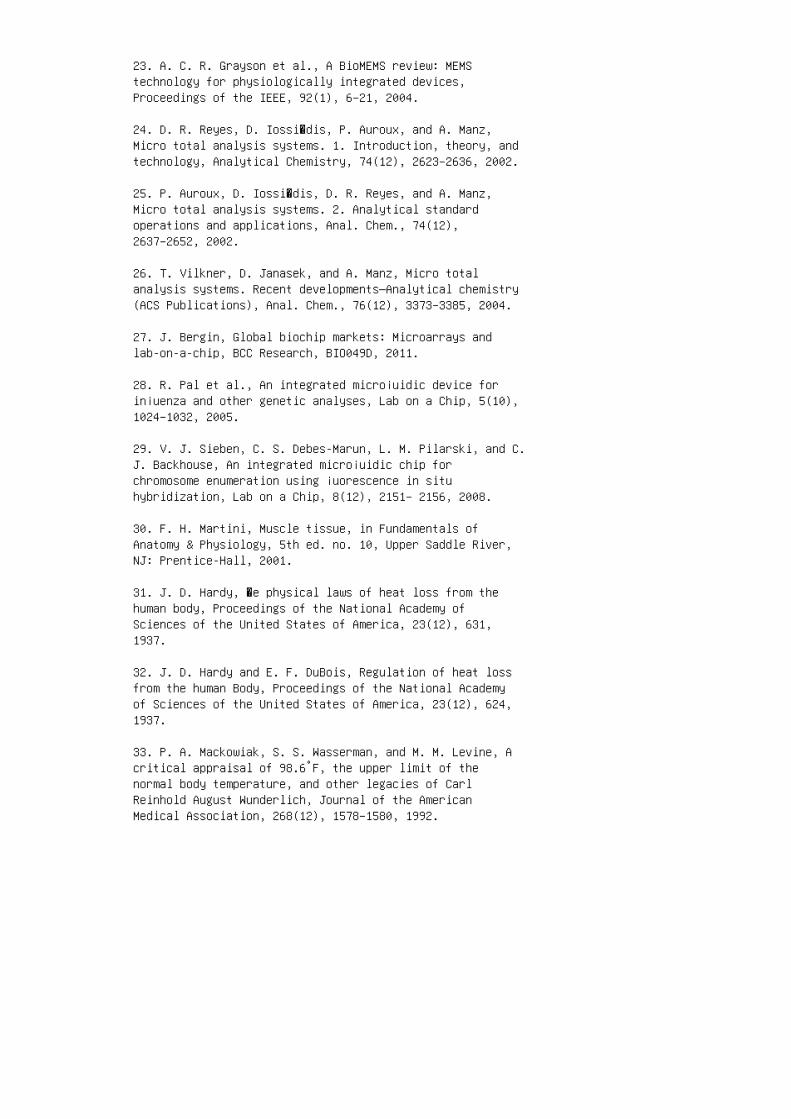
23. A. C. R. Grayson et al., A BioMEMS review: MEMStechnology for physiologically integrated devices,Proceedings of the IEEE, 92(1), 6–21, 2004.
24. D. R. Reyes, D. Iossi�dis, P. Auroux, and A. Manz,Micro total analysis systems. 1. Introduction, theory, andtechnology, Analytical Chemistry, 74(12), 2623–2636, 2002.
25. P. Auroux, D. Iossi�dis, D. R. Reyes, and A. Manz,Micro total analysis systems. 2. Analytical standardoperations and applications, Anal. Chem., 74(12),2637–2652, 2002.
26. T. Vilkner, D. Janasek, and A. Manz, Micro totalanalysis systems. Recent developments—Analytical chemistry(ACS Publications), Anal. Chem., 76(12), 3373–3385, 2004.
27. J. Bergin, Global biochip markets: Microarrays andlab-on-a-chip, BCC Research, BIO049D, 2011.
28. R. Pal et al., An integrated micro¡uidic device forin¡uenza and other genetic analyses, Lab on a Chip, 5(10),1024–1032, 2005.
29. V. J. Sieben, C. S. Debes-Marun, L. M. Pilarski, and C.J. Backhouse, An integrated micro¡uidic chip forchromosome enumeration using ¡uorescence in situhybridization, Lab on a Chip, 8(12), 2151– 2156, 2008.
30. F. H. Martini, Muscle tissue, in Fundamentals ofAnatomy & Physiology, 5th ed. no. 10, Upper Saddle River,NJ: Prentice-Hall, 2001.
31. J. D. Hardy, �e physical laws of heat loss from thehuman body, Proceedings of the National Academy ofSciences of the United States of America, 23(12), 631,1937.
32. J. D. Hardy and E. F. DuBois, Regulation of heat lossfrom the human Body, Proceedings of the National Academyof Sciences of the United States of America, 23(12), 624,1937.
33. P. A. Mackowiak, S. S. Wasserman, and M. M. Levine, Acritical appraisal of 98.6°F, the upper limit of thenormal body temperature, and other legacies of CarlReinhold August Wunderlich, Journal of the AmericanMedical Association, 268(12), 1578–1580, 1992.
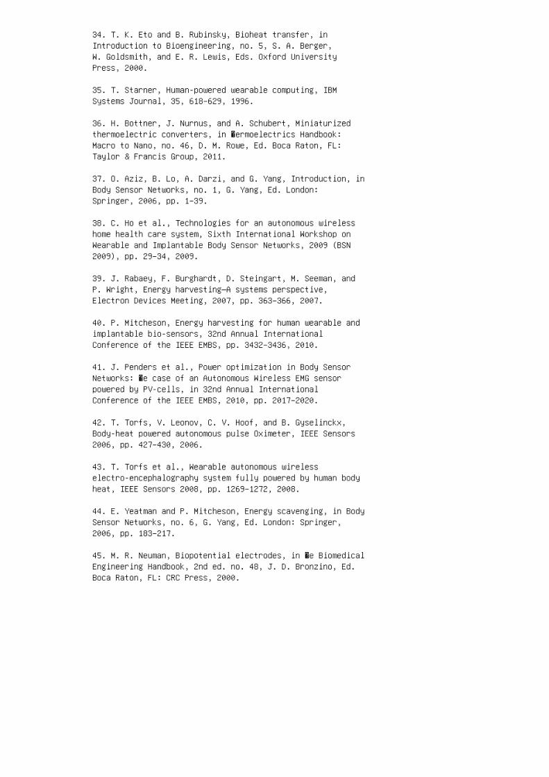
34. T. K. Eto and B. Rubinsky, Bioheat transfer, inIntroduction to Bioengineering, no. 5, S. A. Berger,W. Goldsmith, and E. R. Lewis, Eds. Oxford UniversityPress, 2000.
35. T. Starner, Human-powered wearable computing, IBMSystems Journal, 35, 618–629, 1996.
36. H. Bottner, J. Nurnus, and A. Schubert, Miniaturizedthermoelectric converters, in �ermoelectrics Handbook:Macro to Nano, no. 46, D. M. Rowe, Ed. Boca Raton, FL:Taylor & Francis Group, 2011.
37. O. Aziz, B. Lo, A. Darzi, and G. Yang, Introduction, inBody Sensor Networks, no. 1, G. Yang, Ed. London:Springer, 2006, pp. 1–39.
38. C. Ho et al., Technologies for an autonomous wirelesshome health care system, Sixth International Workshop onWearable and Implantable Body Sensor Networks, 2009 (BSN2009), pp. 29–34, 2009.
39. J. Rabaey, F. Burghardt, D. Steingart, M. Seeman, andP. Wright, Energy harvesting—A systems perspective,Electron Devices Meeting, 2007, pp. 363–366, 2007.
40. P. Mitcheson, Energy harvesting for human wearable andimplantable bio-sensors, 32nd Annual InternationalConference of the IEEE EMBS, pp. 3432–3436, 2010.
41. J. Penders et al., Power optimization in Body SensorNetworks: �e case of an Autonomous Wireless EMG sensorpowered by PV-cells, in 32nd Annual InternationalConference of the IEEE EMBS, 2010, pp. 2017–2020.
42. T. Torfs, V. Leonov, C. V. Hoof, and B. Gyselinckx,Body-heat powered autonomous pulse Oximeter, IEEE Sensors2006, pp. 427–430, 2006.
43. T. Torfs et al., Wearable autonomous wirelesselectro-encephalography system fully powered by human bodyheat, IEEE Sensors 2008, pp. 1269–1272, 2008.
44. E. Yeatman and P. Mitcheson, Energy scavenging, in BodySensor Networks, no. 6, G. Yang, Ed. London: Springer,2006, pp. 183–217.
45. M. R. Neuman, Biopotential electrodes, in �e BiomedicalEngineering Handbook, 2nd ed. no. 48, J. D. Bronzino, Ed.Boca Raton, FL: CRC Press, 2000.
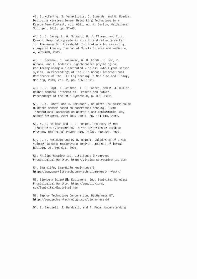
46. B. McCarthy, S. Varakliotis, C. Edwards, and U. Roedig,Deploying Wireless Sensor Networking Technology in aRescue Team Context, vol. 6511, no. 4. Berlin, Heidelberg:Springer, 2010, pp. 37–48.
47. D. G. Carey, L. A. Schwarz, G. J. Pliego, and R. L.Ramond, Respiratory rate is a valid and reliable markerfor the anaerobic threshold: Implications for measuringchange in �tness, Journal of Sports Science and Medicine,4, 482–488, 2005.
48. E. Jovanov, D. Raskovic, A. O. Lords, P. Cox, R.Adhami, and F. Andrasik, Synchronized physiologicalmonitoring using a distributed wireless intelligent sensorsystem, in Proceedings of the 25th Annual InternationalConference of the IEEE Engineering in Medicine and BiologySociety, 2003, vol. 2, pp. 1368–1371.
49. R. W. Hoyt, J. Reifman, T. S. Coster, and M. J. Buller,Combat medical informatics: Present and future,Proceedings of the AMIA Symposium, p. 335, 2002.
50. P. K. Baheti and H. Garudadri, An ultra low power pulseOximeter sensor based on compressed sensing, SixthInternational Workshop on Wearable and Implantable BodySensor Networks, 2009 (BSN 2009), pp. 144–148, 2009.
51. K. J. Heilman and S. W. Porges, Accuracy of thelifeShirt ® (Vivometrics) in the detection of cardiacrhythms, Biological Psychology, 75(3), 300–305, 2007.
52. J. E. McKenzie and D. W. Osgood, Validation of a newtelemetric core temperature monitor, Journal of �ermalBiology, 29, 605–611, 2004.
53. Philips-Respironics, VitalSense IntegratedPhysiological Monitor, http://vitalsense.respironics.com/
54. Smartlife, SmartLife HealthVest ® ,http://www.smartlifetech.com/technology/Health-Vest-/
55. Bio-Lynx Scienti�c Equipment, Inc, Equivital WirelessPhysiological Monitor, http://www.bio-lynx.com/Equivital/Equivital.htm
56. Zephyr Technology Corporation, BioHarness BT,http://www.zephyr-technology.com/bioharness-bt
57. S. Bardzell, J. Bardzell, and T. Pace, Understanding
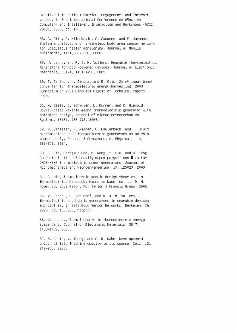
a¤ective interaction: Emotion, engagement, and Internetvideos, in 3rd International Conference on A¶ectiveComputing and Intelligent Interaction and Workshops (ACII2009), 2009, pp. 1–8.
58. C. Otto, A. Milenkovic, C. Sanders, and E. Javanov,System architecture of a wireless body area sensor networkfor ubiquitous health monitoring, Journal of MobileMultimedia, 1(4), 307–326, 2006.
59. V. Leonov and R. J. M. Vullers, Wearable thermoelectricgenerators for body-powered devices, Journal of ElectronicMaterials, 38(7), 1491–1498, 2009.
60. E. Carlson, K. Strunz, and B. Otis, 20 mV input boostconverter for thermoelectric energy harvesting, 2009Symposium on VLSI Circuits Digest of Technical Papers,2009.
61. W. Glatz, E. Schwyter, L. Durrer, and C. Hierold,Bi2Te3-based ¡exible micro thermoelectric generator withoptimized design, Journal of MicroelectromechanicalSystems, 18(3), 763–772, 2009.
62. M. Strasser, R. Aigner, C. Lauterbach, and T. Sturm,Micromachined CMOS thermoelectric generators as on-chippower supply, Sensors & Actuators: A. Physical, 114,362–370, 2004.
63. J. Xie, Chengkuo Lee, M. Wang, Y. Liu, and H. Feng,Characterization of heavily doped polysilicon �lms forCMOS-MEMS thermoelectric power generators, Journal ofMicromechanics and Microengineering, 19, 125029, 2009.
64. G. Min, �ermoelectric module design theories, in�ermoelectrics Handbook: Macro to Nano, no. 11, D. M.Rowe, Ed. Boca Raton, FL: Taylor & Francis Group, 2006.
65. V. Leonov, C. Van Hoof, and R. J. M. Vullers,�ermoelectric and hybrid generators in wearable devicesand clothes, in 2009 Body Sensor Networks, Berkeley, CA,2009, pp. 195–200, http://
66. V. Leonov, �ermal shunts in thermoelectric energyscavengers, Journal of Electronic Materials, 38(7),1483–1490, 2009.
67. S. Gesta, Y. Tseng, and C. R. Kahn, Developmentalorigin of fat: Tracking obesity to its source, Cell, 131,242–256, 2007.
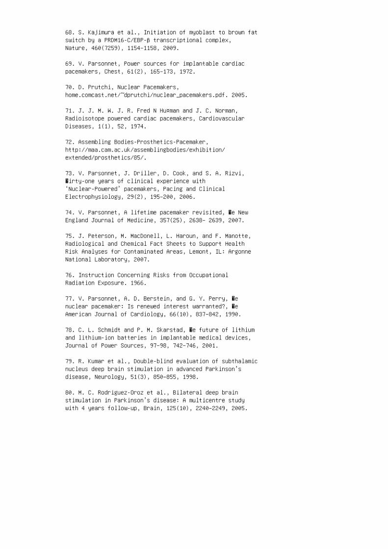
68. S. Kajimura et al., Initiation of myoblast to brown fatswitch by a PRDM16-C/EBP-β transcriptional complex,Nature, 460(7259), 1154–1158, 2009.
69. V. Parsonnet, Power sources for implantable cardiacpacemakers, Chest, 61(2), 165–173, 1972.
70. D. Prutchi, Nuclear Pacemakers,home.comcast.net/~dprutchi/nuclear_pacemakers.pdf. 2005.
71. J. J. M. W. J. R. Fred N Hu¤man and J. C. Norman,Radioisotope powered cardiac pacemakers, CardiovascularDiseases, 1(1), 52, 1974.
72. Assembling Bodies-Prosthetics-Pacemaker,http://maa.cam.ac.uk/assemblingbodies/exhibition/extended/prosthetics/85/.
73. V. Parsonnet, J. Driller, D. Cook, and S. A. Rizvi,�irty-one years of clinical experience with‘Nuclear-Powered’ pacemakers, Pacing and ClinicalElectrophysiology, 29(2), 195–200, 2006.
74. V. Parsonnet, A lifetime pacemaker revisited, �e NewEngland Journal of Medicine, 357(25), 2638– 2639, 2007.
75. J. Peterson, M. MacDonell, L. Haroun, and F. Manotte,Radiological and Chemical Fact Sheets to Support HealthRisk Analyses for Contaminated Areas, Lemont, IL: ArgonneNational Laboratory, 2007.
76. Instruction Concerning Risks from OccupationalRadiation Exposure. 1966.
77. V. Parsonnet, A. D. Berstein, and G. Y. Perry, �enuclear pacemaker: Is renewed interest warranted?, �eAmerican Journal of Cardiology, 66(10), 837–842, 1990.
78. C. L. Schmidt and P. M. Skarstad, �e future of lithiumand lithium-ion batteries in implantable medical devices,Journal of Power Sources, 97–98, 742–746, 2001.
79. R. Kumar et al., Double-blind evaluation of subthalamicnucleus deep brain stimulation in advanced Parkinson’sdisease, Neurology, 51(3), 850–855, 1998.
80. M. C. Rodriguez-Oroz et al., Bilateral deep brainstimulation in Parkinson’s disease: A multicentre studywith 4 years follow-up, Brain, 125(10), 2240–2249, 2005.
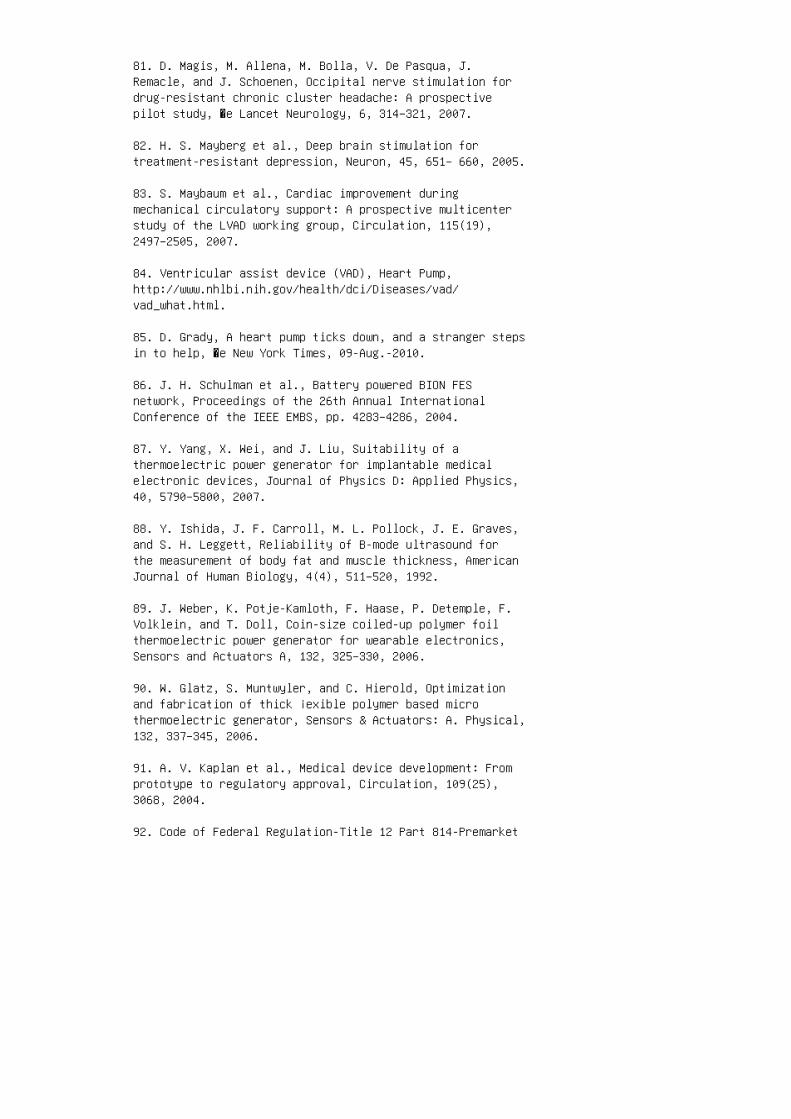
81. D. Magis, M. Allena, M. Bolla, V. De Pasqua, J.Remacle, and J. Schoenen, Occipital nerve stimulation fordrug-resistant chronic cluster headache: A prospectivepilot study, �e Lancet Neurology, 6, 314–321, 2007.
82. H. S. Mayberg et al., Deep brain stimulation fortreatment-resistant depression, Neuron, 45, 651– 660, 2005.
83. S. Maybaum et al., Cardiac improvement duringmechanical circulatory support: A prospective multicenterstudy of the LVAD working group, Circulation, 115(19),2497–2505, 2007.
84. Ventricular assist device (VAD), Heart Pump,http://www.nhlbi.nih.gov/health/dci/Diseases/vad/vad_what.html.
85. D. Grady, A heart pump ticks down, and a stranger stepsin to help, �e New York Times, 09-Aug.-2010.
86. J. H. Schulman et al., Battery powered BION FESnetwork, Proceedings of the 26th Annual InternationalConference of the IEEE EMBS, pp. 4283–4286, 2004.
87. Y. Yang, X. Wei, and J. Liu, Suitability of athermoelectric power generator for implantable medicalelectronic devices, Journal of Physics D: Applied Physics,40, 5790–5800, 2007.
88. Y. Ishida, J. F. Carroll, M. L. Pollock, J. E. Graves,and S. H. Leggett, Reliability of B-mode ultrasound forthe measurement of body fat and muscle thickness, AmericanJournal of Human Biology, 4(4), 511–520, 1992.
89. J. Weber, K. Potje-Kamloth, F. Haase, P. Detemple, F.Volklein, and T. Doll, Coin-size coiled-up polymer foilthermoelectric power generator for wearable electronics,Sensors and Actuators A, 132, 325–330, 2006.
90. W. Glatz, S. Muntwyler, and C. Hierold, Optimizationand fabrication of thick ¡exible polymer based microthermoelectric generator, Sensors & Actuators: A. Physical,132, 337–345, 2006.
91. A. V. Kaplan et al., Medical device development: Fromprototype to regulatory approval, Circulation, 109(25),3068, 2004.
92. Code of Federal Regulation-Title 12 Part 814-Premarket
Approval of Medical Devices. 1986.
93. Code of Federal Regulation-Title 12 Part807-Establishment Registration and Device Listing forManufacturers and Initial Importers of Devices. 1977.
94. FDA-Overview of Device Regulation,http://www.fda.gov/MedicalDevices/DeviceRegulationandGuidance/Overview/default.htm. Center for Devices andRadiological Health.
95. V. S. Mallela, V. Ilankumaran, and N. S. Rao, Trends incardiac pacemaker batteries, Indian Pacing andElectrophysiology Journal, 4(4), 201, 2004.
96. W. N. Rom and S. Markowitz, Environmental andOccupational Medicine, Philadelphia, PA: LippincottWilliams and Wilkins, 2006.
97. N. H. Proctor, G. J. Hathaway, and J. P. Hughes,Proctor and Hughes’ Chemical Hazards of the Workplace, 5thed. NY: John Wiley & Sons, 2004.
98. R. J. Lewis, Sax’s Dangerous Properties of IndustrialMaterials, 11th ed. NY: John Wiley & Sons, 2005.
99. E. L. Schneider and J. M. Guralnik, �e Aging ofAmerica, JAMA: �e Journal of the American MedicalAssociation, 263(17), 2335–2340, 1990.
100. D. C. Angus, M. A. Kelley, R. J. Schmitz, A. White,and J. Popovich, Current and projected workforcerequirements for care of the critically Ill and patientswith pulmonary disease: Can we meet the requirements of anaging population?, JAMA: �e Journal of the American MedicalAssociation, 284(21), 2762–2770, 2000.
101. Older Americans 2010: Key Indicators of Well-Being. �eFederal Interagency Forum on AgingRelated Statistics, 2010.
102. World Population Ageing 2009. United Nations, 2009.
103. E. W. Ford, N. Menachemi, and M. T. Phillips,Predicting the adoption of electronic health records byphysicians: When will health care be paperless?, Journal ofthe American Medical Informatics Association, 13(1),106–112, 2006.
104. Fact Sheet: GE, Intel to Form New Healthcare JointVenture, download.intel.com/pressroom/pdf/
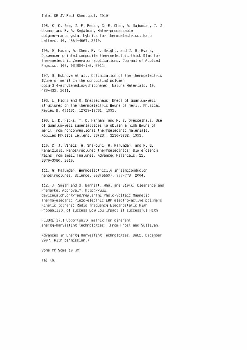
Intel_GE_JV_Fact_Sheet.pdf. 2010.
105. K. C. See, J. P. Feser, C. E. Chen, A. Majumdar, J. J.Urban, and R. A. Segalman, Water-processablepolymer−nanocrystal hybrids for thermoelectrics, NanoLetters, 10, 4664–4667, 2010.
106. D. Madan, A. Chen, P. K. Wright, and J. W. Evans,Dispenser printed composite thermoelectric thick �lms forthermoelectric generator applications, Journal of AppliedPhysics, 109, 034804-1-6, 2011.
107. O. Bubnova et al., Optimization of the thermoelectric�gure of merit in the conducting polymerpoly(3,4-ethylenedioxythiophene), Nature Materials, 10,429–433, 2011.
108. L. Hicks and M. Dresselhaus, E¤ect of quantum-wellstructures on the thermoelectric �gure of merit, PhysicalReview B, 47(19), 12727–12731, 1993.
109. L. D. Hicks, T. C. Harman, and M. S. Dresselhaus, Useof quantum–well superlattices to obtain a high �gure ofmerit from nonconventional thermoelectric materials,Applied Physics Letters, 63(23), 3230–3232, 1993.
110. C. J. Vineis, A. Shakouri, A. Majumdar, and M. G.Kanatzidis, Nanostructured thermoelectrics: Big e´ciencygains from small features, Advanced Materials, 22,3970–3980, 2010.
111. A. Majumdar, �ermoelectricity in semiconductornanostructures, Science, 303(5659), 777–778, 2004.
112. J. Smith and S. Barrett, What are 510(k) Clearance andPremarket Approval?, http://www.devicewatch.org/reg/reg.shtml Photo-voltaic MagneticThermo-electric Piezo-electric EAP electro-active polymersKinetic (others) Radio frequency Electrostatic HighProbability of success Low Low Impact if successful High
FIGURE 17.1 Opportunity matrix for di¤erentenergy-harvesting technologies. (From Frost and Sullivan.
Advances in Energy Harvesting Technologies, DoC2, December2007. With permission.)
Some mm Some 10 µm
(a) (b)
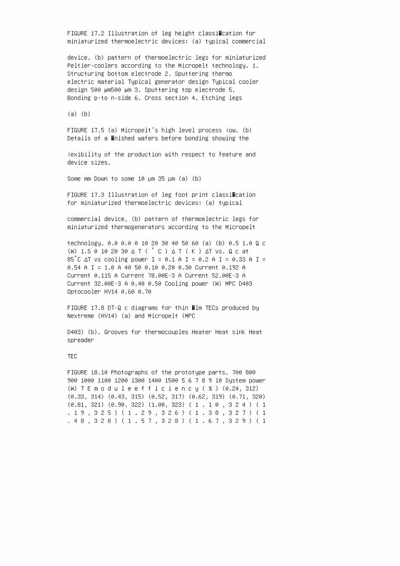
FIGURE 17.2 Illustration of leg height classi�cation forminiaturized thermoelectric devices: (a) typical commercial
device, (b) pattern of thermoelectric legs for miniaturizedPeltier-coolers according to the Micropelt technology. 1.Structuring bottom electrode 2. Sputtering thermoelectric material Typical generator design Typical coolerdesign 500 μm500 μm 3. Sputtering top electrode 5.Bonding p-to n-side 6. Cross section 4. Etching legs
(a) (b)
FIGURE 17.5 (a) Micropelt’s high level process ¡ow. (b)Details of a �nished wafers before bonding showing the
¡exibility of the production with respect to feature anddevice sizes.
Some mm Down to some 10 µm 35 µm (a) (b)
FIGURE 17.3 Illustration of leg foot print classi�cationfor miniaturized thermoelectric devices: (a) typical
commercial device, (b) pattern of thermoelectric legs forminiaturized thermogenerators according to the Micropelt
technology. 0.0 0.0 0 10 20 30 40 50 60 (a) (b) 0.5 1.0 Q c(W) 1.5 0 10 20 30 Δ T ( ° C ) Δ T ( K ) ΔT vs. Q c at85°C ΔT vs cooling power I = 0.1 A I = 0.2 A I = 0.33 A I =0.54 A I = 1.0 A 40 50 0.10 0.20 0.30 Current 0.192 ACurrent 0.115 A Current 78.00E-3 A Current 52.00E-3 ACurrent 32.00E-3 A 0.40 0.50 Cooling power (W) MPC D403Optocooler HV14 0.60 0.70
FIGURE 17.8 DT-Q c diagrams for thin �lm TECs produced byNextreme (HV14) (a) and Micropelt (MPC
D403) (b). Grooves for thermocouples Heater Heat sink Heatspreader
TEC
FIGURE 18.10 Photographs of the prototype parts. 700 800900 1000 1100 1200 1300 1400 1500 5 6 7 8 9 10 System power(W) T E m o d u l e e f f i c i e n c y ( % ) (0.24, 312)(0.33, 314) (0.43, 315) (0.52, 317) (0.62, 319) (0.71, 320)(0.81, 321) (0.90, 322) (1.00, 323) ( 1 . 1 0 , 3 2 4 ) ( 1. 1 9 , 3 2 5 ) ( 1 . 2 9 , 3 2 6 ) ( 1 . 3 8 , 3 2 7 ) ( 1. 4 8 , 3 2 8 ) ( 1 . 5 7 , 3 2 8 ) ( 1 . 6 7 , 3 2 9 ) ( 1
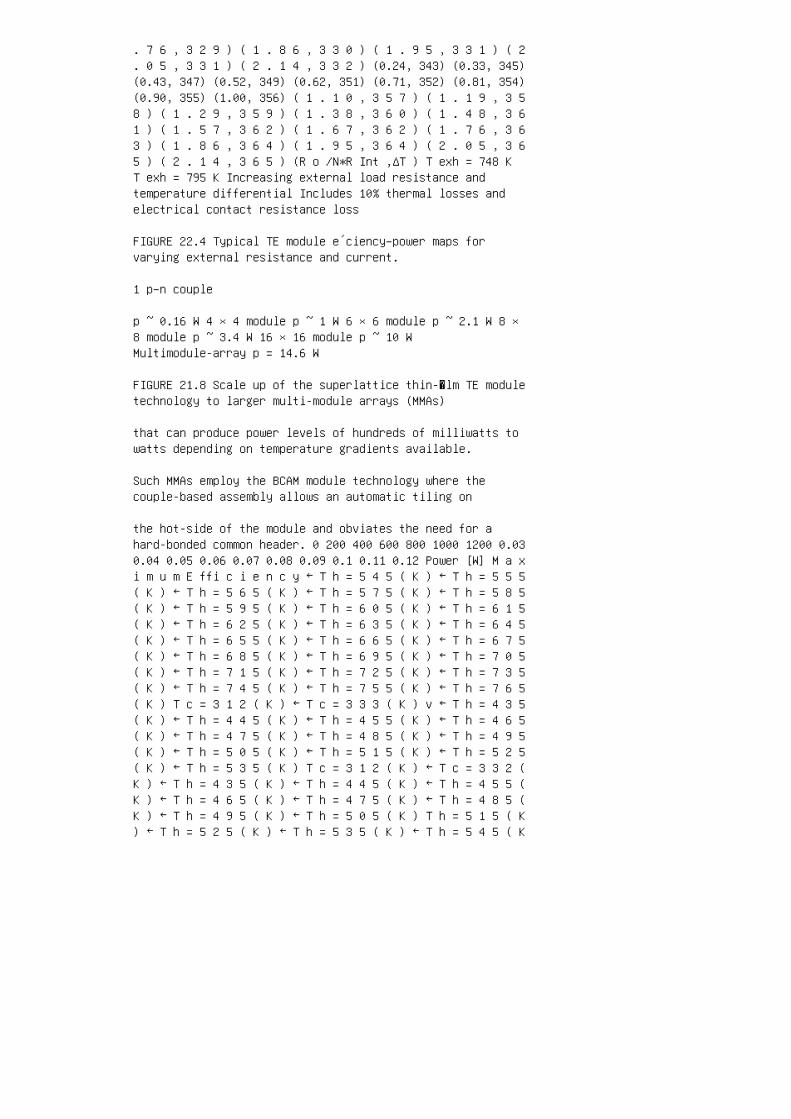
. 7 6 , 3 2 9 ) ( 1 . 8 6 , 3 3 0 ) ( 1 . 9 5 , 3 3 1 ) ( 2
. 0 5 , 3 3 1 ) ( 2 . 1 4 , 3 3 2 ) (0.24, 343) (0.33, 345)(0.43, 347) (0.52, 349) (0.62, 351) (0.71, 352) (0.81, 354)(0.90, 355) (1.00, 356) ( 1 . 1 0 , 3 5 7 ) ( 1 . 1 9 , 3 58 ) ( 1 . 2 9 , 3 5 9 ) ( 1 . 3 8 , 3 6 0 ) ( 1 . 4 8 , 3 61 ) ( 1 . 5 7 , 3 6 2 ) ( 1 . 6 7 , 3 6 2 ) ( 1 . 7 6 , 3 63 ) ( 1 . 8 6 , 3 6 4 ) ( 1 . 9 5 , 3 6 4 ) ( 2 . 0 5 , 3 65 ) ( 2 . 1 4 , 3 6 5 ) (R o /N*R Int ,ΔT ) T exh = 748 KT exh = 795 K Increasing external load resistance andtemperature differential Includes 10% thermal losses andelectrical contact resistance loss
FIGURE 22.4 Typical TE module e´ciency–power maps forvarying external resistance and current.
1 p–n couple
p ~ 0.16 W 4 × 4 module p ~ 1 W 6 × 6 module p ~ 2.1 W 8 ×8 module p ~ 3.4 W 16 × 16 module p ~ 10 WMultimodule-array p = 14.6 W
FIGURE 21.8 Scale up of the superlattice thin-�lm TE moduletechnology to larger multi-module arrays (MMAs)
that can produce power levels of hundreds of milliwatts towatts depending on temperature gradients available.
Such MMAs employ the BCAM module technology where thecouple-based assembly allows an automatic tiling on
the hot-side of the module and obviates the need for ahard-bonded common header. 0 200 400 600 800 1000 1200 0.030.04 0.05 0.06 0.07 0.08 0.09 0.1 0.11 0.12 Power [W] M a xi m u m E ffi c i e n c y ← T h = 5 4 5 ( K ) ← T h = 5 5 5( K ) ← T h = 5 6 5 ( K ) ← T h = 5 7 5 ( K ) ← T h = 5 8 5( K ) ← T h = 5 9 5 ( K ) ← T h = 6 0 5 ( K ) ← T h = 6 1 5( K ) ← T h = 6 2 5 ( K ) ← T h = 6 3 5 ( K ) ← T h = 6 4 5( K ) ← T h = 6 5 5 ( K ) ← T h = 6 6 5 ( K ) ← T h = 6 7 5( K ) ← T h = 6 8 5 ( K ) ← T h = 6 9 5 ( K ) ← T h = 7 0 5( K ) ← T h = 7 1 5 ( K ) ← T h = 7 2 5 ( K ) ← T h = 7 3 5( K ) ← T h = 7 4 5 ( K ) ← T h = 7 5 5 ( K ) ← T h = 7 6 5( K ) T c = 3 1 2 ( K ) ← T c = 3 3 3 ( K ) v ← T h = 4 3 5( K ) ← T h = 4 4 5 ( K ) ← T h = 4 5 5 ( K ) ← T h = 4 6 5( K ) ← T h = 4 7 5 ( K ) ← T h = 4 8 5 ( K ) ← T h = 4 9 5( K ) ← T h = 5 0 5 ( K ) ← T h = 5 1 5 ( K ) ← T h = 5 2 5( K ) ← T h = 5 3 5 ( K ) T c = 3 1 2 ( K ) ← T c = 3 3 2 (K ) ← T h = 4 3 5 ( K ) ← T h = 4 4 5 ( K ) ← T h = 4 5 5 (K ) ← T h = 4 6 5 ( K ) ← T h = 4 7 5 ( K ) ← T h = 4 8 5 (K ) ← T h = 4 9 5 ( K ) ← T h = 5 0 5 ( K ) T h = 5 1 5 ( K) ← T h = 5 2 5 ( K ) ← T h = 5 3 5 ( K ) ← T h = 5 4 5 ( K
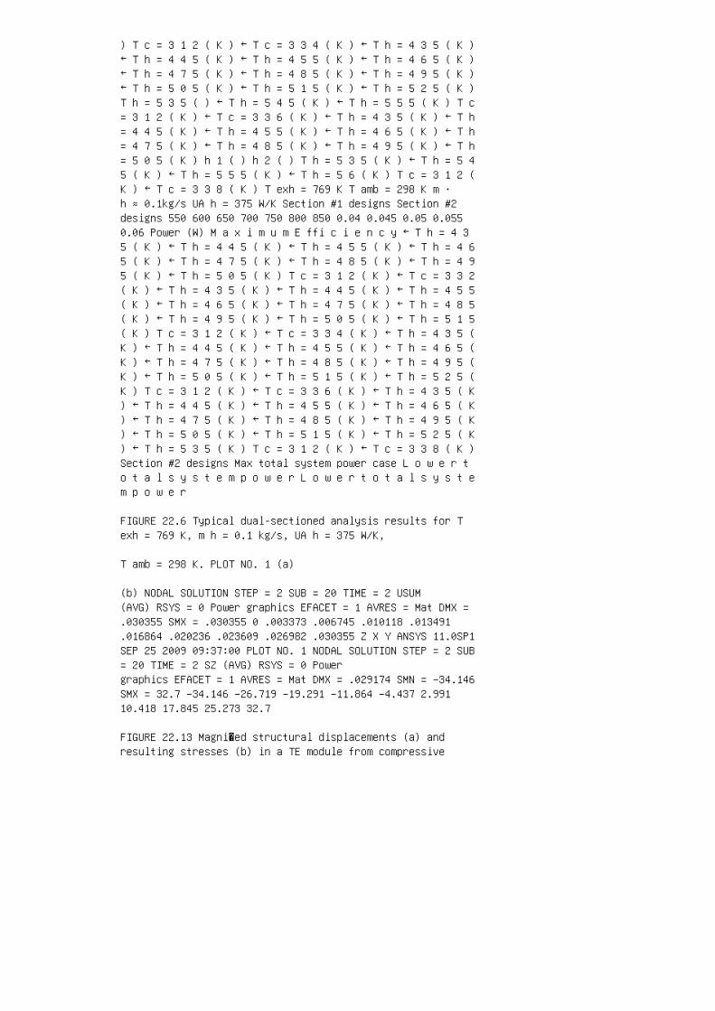
) T c = 3 1 2 ( K ) ← T c = 3 3 4 ( K ) ← T h = 4 3 5 ( K )← T h = 4 4 5 ( K ) ← T h = 4 5 5 ( K ) ← T h = 4 6 5 ( K )← T h = 4 7 5 ( K ) ← T h = 4 8 5 ( K ) ← T h = 4 9 5 ( K )← T h = 5 0 5 ( K ) ← T h = 5 1 5 ( K ) ← T h = 5 2 5 ( K )T h = 5 3 5 ( ) ← T h = 5 4 5 ( K ) ← T h = 5 5 5 ( K ) T c= 3 1 2 ( K ) ← T c = 3 3 6 ( K ) ← T h = 4 3 5 ( K ) ← T h= 4 4 5 ( K ) ← T h = 4 5 5 ( K ) ← T h = 4 6 5 ( K ) ← T h= 4 7 5 ( K ) ← T h = 4 8 5 ( K ) ← T h = 4 9 5 ( K ) ← T h= 5 0 5 ( K ) h 1 ( ) h 2 ( ) T h = 5 3 5 ( K ) ← T h = 5 45 ( K ) ← T h = 5 5 5 ( K ) ← T h = 5 6 ( K ) T c = 3 1 2 (K ) ← T c = 3 3 8 ( K ) T exh = 769 K T amb = 298 K m ·h ≈ 0.1kg/s UA h = 375 W/K Section #1 designs Section #2designs 550 600 650 700 750 800 850 0.04 0.045 0.05 0.0550.06 Power (W) M a x i m u m E ffi c i e n c y ← T h = 4 35 ( K ) ← T h = 4 4 5 ( K ) ← T h = 4 5 5 ( K ) ← T h = 4 65 ( K ) ← T h = 4 7 5 ( K ) ← T h = 4 8 5 ( K ) ← T h = 4 95 ( K ) ← T h = 5 0 5 ( K ) T c = 3 1 2 ( K ) ← T c = 3 3 2( K ) ← T h = 4 3 5 ( K ) ← T h = 4 4 5 ( K ) ← T h = 4 5 5( K ) ← T h = 4 6 5 ( K ) ← T h = 4 7 5 ( K ) ← T h = 4 8 5( K ) ← T h = 4 9 5 ( K ) ← T h = 5 0 5 ( K ) ← T h = 5 1 5( K ) T c = 3 1 2 ( K ) ← T c = 3 3 4 ( K ) ← T h = 4 3 5 (K ) ← T h = 4 4 5 ( K ) ← T h = 4 5 5 ( K ) ← T h = 4 6 5 (K ) ← T h = 4 7 5 ( K ) ← T h = 4 8 5 ( K ) ← T h = 4 9 5 (K ) ← T h = 5 0 5 ( K ) ← T h = 5 1 5 ( K ) ← T h = 5 2 5 (K ) T c = 3 1 2 ( K ) ← T c = 3 3 6 ( K ) ← T h = 4 3 5 ( K) ← T h = 4 4 5 ( K ) ← T h = 4 5 5 ( K ) ← T h = 4 6 5 ( K) ← T h = 4 7 5 ( K ) ← T h = 4 8 5 ( K ) ← T h = 4 9 5 ( K) ← T h = 5 0 5 ( K ) ← T h = 5 1 5 ( K ) ← T h = 5 2 5 ( K) ← T h = 5 3 5 ( K ) T c = 3 1 2 ( K ) ← T c = 3 3 8 ( K )Section #2 designs Max total system power case L o w e r to t a l s y s t e m p o w e r L o w e r t o t a l s y s t em p o w e r
FIGURE 22.6 Typical dual-sectioned analysis results for Texh = 769 K, m h = 0.1 kg/s, UA h = 375 W/K,
T amb = 298 K. PLOT NO. 1 (a)
(b) NODAL SOLUTION STEP = 2 SUB = 20 TIME = 2 USUM(AVG) RSYS = 0 Power graphics EFACET = 1 AVRES = Mat DMX =.030355 SMX = .030355 0 .003373 .006745 .010118 .013491.016864 .020236 .023609 .026982 .030355 Z X Y ANSYS 11.0SP1SEP 25 2009 09:37:00 PLOT NO. 1 NODAL SOLUTION STEP = 2 SUB= 20 TIME = 2 SZ (AVG) RSYS = 0 Powergraphics EFACET = 1 AVRES = Mat DMX = .029174 SMN = –34.146SMX = 32.7 –34.146 –26.719 –19.291 –11.864 –4.437 2.99110.418 17.845 25.273 32.7
FIGURE 22.13 Magni�ed structural displacements (a) andresulting stresses (b) in a TE module from compressive
and expansive forces (displacements in mm, stresses inMPa). 0 10 20 30 40 C o s t ( £ ) p e r w a t t 50 (dt = 80K) 42.06 31.55 31.38 24.00 14.34 11.77 5.00 4.49 4.42 3.1212.74 11.98 18.93 63.39 11.90 12.50 60 70
FIGURE 23.6 Cost per watt. 0 0.0 0.2 0.4 0.6 0.8 M o d u le p o w e r o u t p u t ( W ) 1.0 1.2 1.4 1.6 1.8 2.0 10 2030 40 50 60 70 80 90 Temperature difference
FIGURE 23.7 Corresponding power output.
FIGURE 23.11 �ermoelectric generator. (T. Kajikawa, ShonanInstitute of Technology.)
FIGURE 23.10 �e Kusatsu hot spring. (T. Kajikawa, ShonanInstitute of Technology.) Latitude 40°N 40°E 80°E 120°E160°E Longitude 160°W120°W80°W 40°W 0°W 20°N Equator 20°S40°S Less than 18°C 22° to 24°C More than 24°C Depth lessthan 1000 m 18° to 20°C 20° to 22°C Temperature differencebetween surface and depth of 1000 m
FIGURE 23.16 Ocean temperature gradient.


