Embed Size (px)
Citation preview

Optical Characterization of Compound Semiconductors UsingPhotoconductivity and Photoreflectance
Vladimir A. Stoica
Thesis submitted to Eberly College of Arts and Sciencesat West Virginia University
in partial fulfillment of the requirementsfor the degree of
Master of Sciencein
Physics
Thomas H. Myers, Ph.D. ChairLarry E. Halliburton, Ph.D.
David Lederman, Ph.D.
Department of Physics
Morgantown, West Virginia2000
Keywords: Photoreflectance, Photoconductivity, GaN, CdZnTe, Mapping

ii
ABSTRACT
Optical Characterization of Compound Semiconductors UsingPhotoconductivity and Photoreflectance
Vladimir A. Stoica
Custom photoreflectance modulation spectroscopy and photoconductivity spectroscopy set-ups
were constructed and used to characterize semiconductor materials. The ternary Cd1-xZnxTe
compound was studied to achieve fine control over its composition to provide lattice-matched
substrates for the growth of Hg1-xCdxTe which is used in infrared detectors. Photoreflectance
spectroscopy, capable of accurate estimations of energy levels in semiconductors, was applied to
determine composition in CdZnTe standards via band gap energy determinations. The excitonic
contributions at room temperature were shown to be in agreement with literature data. The lack
of lattice matched substrates for the growth of GaN is still providing material with considerable
defect densities despite substantial efforts in material research to date. Photoconductivity
spectroscopy was used to characterize various epitaxially grown GaN samples via studying
defects and imperfections present in the material. Distinct photoconductance features were
observed near the GaN band edge, being attributed to sub-band imperfection levels.

iii
Acknowledgments
I am truly indebted to my wife and life partner, Dana, for her uninterrupted love, patience
and encouragement that made possible my whole dedication toward the present study.
My deepest appreciation and gratitude is dedicated to my research advisor, Dr. Thomas
H. Myers. I recognize that he is a preeminent professor and specialist as well as being a good
person, providing me continuous support and guidance along the whole way of this work. He has
set a positive example that is one I haven’t encountered many times in my life and one I will
never forget.
I would like to thank Dr. Nancy Giles and Dr. Larry Halliburton for providing me
assistance through the use of their lab equipment or data taken in their labs. I would also like to
thank Luke Holbert and Dr. Monica Moldovan for doing experiments and providing me data that
represent important complementary information to the methods I used.
Special thanks go out to Aaron Ptak not only for growth and preparation of the samples
but also for useful discussions related to the common research area.
I would like to acknowledge Dr. Larry Halliburton and Dr. David Lederman for taking
the time to serve on my committee. Especially, I want to thank to Dr. David Lederman for
spending a lot of time with me discussing research-related matters.
Finally, I thank my family and my colleagues and teachers around the department that
helped and supported me during my study.
The work performed on GaN was supported by the Office of Naval Research on Grant
N00014-96-1-1008. The work performed on CdZnTe was part of a National Institute of
Advanced Technology Program, “Chemical Imaging for Semiconductor Metrology”, in
collaboration with eV-Products, Inc. and ChemIcon, Inc.

iv
Table of Contents
Abstract. . . . . . . . . . . . . . . . . . . . . . . . . . . . . . . . . . . . . . . . . . . . . . . . . . . . . . . . . . . . . . . . . . . . . .ii
Acknowledgments . . . . . . . . . . . . . . . . . . . . . . . . . . . . . . . . . . . . . . . . . . . . . . . . . . . . . . . . . . . . .iii
Table of Contents. . . . . . . . . . . . . . . . . . . . . . . . . . . . . . . . . . . . . . . . . . . . . . . . . . . . . . . . . . . . . . iv
1. Introduction . . . . . . . . . . . . . . . . . . . . . . . . . . . . . . . . . . . . . . . . . . . . . . . . . . . . . . . . . . . . . . .1
1.1 Impact of Semiconductor Research . . . . . . . . . . . . . . . . . . . . . . . . . . . . . . . . . . . . . . . . . 1
1.2 The Potential of Gallium Nitride. . . . . . . . . . . . . . . . . . . . . . . . . . . . . . . . . . . . . . . . . . . . 1
1.3 CdTe and CdZnTe Materials for Detectors . . . . . . . . . . . . . . . . . . . . . . . . . . . . . . . . . . . .3
1.4 Objectives and Goals . . . . . . . . . . . . . . . . . . . . . . . . . . . . . . . . . . . . . . . . . . . . . . . . . . . . .4
2. Theory. . . . . . . . . . . . . . . . . . . . . . . . . . . . . . . . . . . . . . . . . . . . . . . . . . . . . . . . . . . . . . . . . . . .6
2.1 Photoreflectance Modulation Spectroscopy . . . . . . . . . . . . . . . . . . . . . . . . . . . . . . . . . . . .6
2.2 Photoconductivity Spectroscopy . . . . . . . . . . . . . . . . . . . . . . . . . . . . . . . . . . . . . . . . . . . 11
3. Experimental details . . . . . . . . . . . . . . . . . . . . . . . . . . . . . . . . . . . . . . . . . . . . . . . . . . . . . . 15
3.1 Basic Set-up . . . . . . . . . . . . . . . . . . . . . . . . . . . . . . . . . . . . . . . . . . . . . . . . . . . . . . . . . . .15
3.2 Photoreflectance Set-up . . . . . . . . . . . . . . . . . . . . . . . . . . . . . . . . . . . . . . . . . . . . . . . . . 18
3.3 Photoconductivity Set-up . . . . . . . . . . . . . . . . . . . . . . . . . . . . . . . . . . . . . . . . . . . . . . . . 27
4. Results . . . . . . . . . . . . . . . . . . . . . . . . . . . . . . . . . . . . . . . . . . . . . . . . . . . . . . . . . . . . . . . . . . 32
4.1 Concentration determination of small amounts of Zn in Cd1-xZnxTe bulk semiconductors
using photoreflectance spectroscopy . . . . . . . . . . . . . . . . . . . . . . . . . . . . . . . . . . . . . . . .48
4.2 Photoconductivity spectroscopy studies of epitaxially grown GaN using various growth
methods . . . . . . . . . . . . . . . . . . . . . . . . . . . . . . . . . . . . . . . . . . . . . . . . . . . . . . . . . . . . . . 61
5. Summary and suggested future research . . . . . . . . . . . . . . . . . . . . . . . . . . . . . . . . . . . . . . 65
References . . . . . . . . . . . . . . . . . . . . . . . . . . . . . . . . .. . . . . . . . . . .. . . . . . . . . . .. . .. . . . .. . . . . .67

1
1. INTRODUCTION
1.1 Impact of Semiconductor Research
In the last century considerable advances have been realized in the research and
applications of semiconductors. It is well known that semiconductor technology has a great
impact on our society. We know the power of television or the personal computers that are in
almost everyone’s house or office, changing the way we communicate. Semiconductor
applications are present everywhere around us: on roads, in houses, on your desk, even in your
pocket. When a new material or semiconductor device is produced, it often opens never before
imagined gates or connections that influence your life. This immediate application is why
semiconductor research attracts more and more interest at all scientific levels.
1.2 The Potential of Gallium Nitride
More than a promising material for optoelectronics and electronics, GaN already
represents an economic reality. Widely explored in the last ten years, with a publication rate that
increased by more than 200 % each year, GaN development has gone from an exploratory
research activity to producing an industrial product. Tremendous effort has been carried out to
understand the physical properties of nitrides so that this has been by far the most active
semiconductor research field during the latter part of this decade.1
Due to promising properties such as excellent conductivity, large breakdown field, and
resistance to chemical attack, GaN represents an ideal candidate for electronic devices capable of
operation at high power levels, high temperatures and in caustic environments. The need to
tolerate high temperature and hostile environments required by industry application including
aerospace, automotive, petroleum and others has stimulated many researchers to turn their
attention to GaN as a material candidate to meet these requirements.2 GaN transistors have
already been demonstrated3 that work at temperatures up to 600 oC.
Increased attention toward the wide band gap semiconductors such as GaN is also due in
part to the desire to create electro-optical devices operating at blue and ultraviolet (UV)
wavelengths. Development of semiconductor device technology for applications in the blue

2
region of the electromagnetic spectrum would allow production of the three primary colors of the
visible spectrum that would have a major impact on graphic and imaging applications.
Many companies are working on nitride lasers for optical storage, since their short
wavelength produces a smaller spot size when the beam is focused by an optical system. This
smaller laser spot can read and write features which are closer together, allowing more data
marks to be put into the disk. Since the diffraction-limited spot size is proportional to the laser
wavelength, which in case of GaN is about 360 nm, such UV light allows a spot smaller than
today's widely used lasers, which typically use infrared light (780 to 850 nm) or red light (650 to
670 nm).4 The recently produced GaN-based blue lasers operating at a shorter wavelength (460
to 410 nm) already have the capability to overcome performance limitations of the classical red
lasers used for the optical storage of information. In addition, the shorter wavelength of the blue
laser can also be used in laser printers to increase the resolution. The predicted increase in the
amount of information stored using blue lasers is by a factor of 20 for the case of CDs and by a
factor of 6 in case of DVDs. Although blue lasers based on solid state technology have
demonstrated the advantage of blue or UV light, they are not light and compact enough for
consumer electronics. Research is ongoing to produce semiconductor laser diodes (LDs) and
light emitting diodes (LEDs) that offer a better cost/performance/size solution.5 The most
successful material used to produce green and blue LEDs is InGaN, completely dominating the
market. White and yellow LEDs using GaN are also being commercialized. These products, with
high light emission efficiency, should find wide use in applications such as full color displays,
traffic signs and automobile and aircraft lighting.6 Violet LDs with continuous wave operation
have also been recently demonstrated, having a lasing output power of 5 mW.7
Wide band gap compounds using GaN have important applications in communications.
By creating lasing and detection devices that operate in the 240-280 nm range, the earth’s
atmosphere could be used as an effective communications screen. This is due to the large degree
of absorption of the ozone layer in this wavelength range that renders the atmosphere nearly
opaque to these devices. This would allow space to space communications to be secure from the
earth and also allow imaging array detectors to provide sensitive surveillance of objects coming
up through the atmosphere.8
Also of great importance are GaN photoconductive devices that are highly suited as
solar-blind UV photodetectors for applications such as missile detection, flame sensing and solar

3
UV monitoring. GaN-based materials are ideal for these applications due to their wide and direct
band gaps, making detectors transparent to visible and infrared radiation.9,10 For the case of
military application such as missile launching detection, tracking and interception, the detectivity
has to be extremely large, and the spectral selectivity (how well it rejects solar light) must be as
high as possible. This means that the spectral response of the device should have a flat
responsivity with a sharp band edge transition and no discernable responsivity below the band
gap, which is an important property for solar-blind detectors. In civilian applications, flame
detectors and sensors are needed for monitoring the combustion in large industrial burners and
boilers. In order to observe the flame in a daylight environment, solar blind detectors are needed.
In the deeper ultraviolet (225 to 275 nm), pilot landing aid systems have been proposed based on
UV lights put on the edges of runways and taxiways, with a UV camera on board. Since this
wavelength is much smaller than rain or fog particles, the light can propagate over reasonable
distances. Initial evaluation has shown that visibility can gain a factor of three when going from
visible to the ultraviolet. Another application for UV detectors is the dosimeter for personal use
in UV-rich environments such as beaches or mountains.
Looking at the main applications produced to the date, the field of GaN has been and will
remain in the near future driven by optical sources and detectors in the violet, blue and green,
where other choices of materials have failed to provide similar performance. The market for GaN
based optoelectronic products exists with the potential for large production volumes. At the same
time, other applications are still under development and will take advantage of the large progress
made in the area of optoelectronics.1
1.3 CdTe and CdZnTe Materials for Detectors
Considerable progress has been made in II-VI semiconductor material and in methods for
improving performance of the associated radiation detectors. New high-resistivity CdZnTe
(CZT) material, contact technologies, detector structures, and electronic correction methods have
opened the field of nuclear and x-ray imaging for industrial and medical applications. The
physical properties of CdTe (CT), including its unique combination of high atomic number
providing good photon quantum efficiency, wide band gap and high resistivity leading to low
leakage currents, good lifetime-mobility product and room temperature operation, make it an

4
attractive material for x-ray and γ-ray detectors. Keeping in mind the quality and properties of
the crystals required by the applications, advances were made in the growth of bulk CdTe or
Cd1-xZnxTe using new methods such as the one recently developed by Digirad, Inc. and eV-
Products, Inc. based on the high pressure Bridgeman method (HPBM).11
With recent success made by the crystal growers, a large variety of detection applications
using CT and CZT materials are possible at the present in the fields of medicine, industry,
astronomy and security.11-14 Spectrometers using CT and CZT are considered as a replacement to
scintillation detectors, since they posses a higher energy resolution. Although CT and CZT
detectors have been already demonstrated, continuing effort is still underway to improve the
characteristics of both CT and CZT materials in order to achieve reproducible detectors.
Beside the detection application of CZT materials, this ternary semiconductor alloy also
has promising applications in a variety of solid state devices such as solar cells and light emitting
diodes because its band gap is tunable from 1.5 to 2.3 eV by controlling the stoichiometry.
Moreover, at the present, Cd1-xZnxTe substrates are the favored material for epitaxial deposition
of the important infrared detector material Hg1-xCdxTe (MCT). Its popularity relies on the
possibility of lattice matching and has been found that using Cd1-xZnxTe with x ≈ 0.04 optimizes
lattice matching between these two crystals. In this situation, improvements in the material
quality can be obtained by reducing the density of defects associated with misfit dislocations in
the MCT layer.15 This critical need to produce high quality CZT material and its later use as a
substrate for epitaxial growth results in the need for contactless and nondestructive
characterization techniques. The proposed techniques should be capable of revealing the required
structural or optical properties for the applications mentioned above, and at the same time to
provide fine control over the composition, which is necessary to achieve such applications.
1.4 Objectives and Goals
Automation of experimental systems capable of collecting large amounts of data is an
efficient approach helping the researcher to make rapid progress toward a specific goal. Not only
the continuously increasing number of samples produced by molecular beam epitaxy (MBE)
growers from West Virginia University but also the number of samples coming from other labs

5
has introduced the necessity to quickly investigate individual sample characteristics. This helps
optimize the growth processes in order to obtain high quality materials.
Optical characterization methods for analyzing semiconducting materials have been
successfully used in the past such as spectral photoconductivity16 (SPC) and modulation
photoreflectance17 (PR) techniques. These two methods proved to be an effective method of
determining the sample quality and revealing the role of imperfections or impurities, which is in
agreement with West Virginia University MBE Lab characterization necessities. At the same
time the PR technique is a tool capable of making accurate determination of the band gap
energies of compound semiconductors which are directly correlated with the relative
composition.
Accordingly, the following goals were determined, which motivated the research
presented in this thesis:
1. To construct a custom PR set-up capable of accurately determining energy levels in
semiconductors.
2. To construct a custom SPC setup to study optical properties of GaN to reveal impurity and
defect states in the band gap and to correlate these features with other optical characterization
techniques.
3. To characterize a set of CdZnTe standards by determining and mapping the sample
composition across the surface, using the capability for accurate band gap determination of
the PR technique

6
2. THEORY
2.1 Photoreflectance Modulation Spectroscopy
The photoreflectance technique is a modulation spectroscopy based on very general
principles of experimental physics. Instead of directly measuring the optical spectrum
(reflectance or transmittance), the derivative with respect to some parameter is evaluated. This
can be accomplished by modulating some property of the sample or measuring a system in a
periodic fashion and measuring the corresponding change in the reflectance. Examples of the
perturbations, which correspond to different modulation methods, are changes in the electric or
magnetic field, heat pulse, or uniaxial stress. Such repetitive perturbations modify the spectral
response of the sample, giving rise to differential-like spectra in the region where optical
excitation processes occur. Because of this derivative-like nature, a large number of sharp
spectral features can be observed in modulated reflectance spectra of semiconductors even at
room temperature. With these sharp, well-resolved spectra, it is possible to analyze and directly
yield the properties of the material under study. Changes in reflectance as small as 10-6-10-7 can
be observed using phase -sensitive techniques. The ability to perform a lineshape fit is one of the
great advantages of photoreflectance modulation spectroscopy. Since, for the modulated signal,
the features are localized in photon energy, it is possible to account for the lineshapes to yield
accurate values of important parameters such as energies and broadening functions of interband
(intersubband) transitions. For example, even at 300 K it is possible to obtain the energy of a
particular feature to within a few meV. The extensive fundamental experimental and theoretical
work in the area of modulation spectroscopy during the last 25 years, particularly the
electroreflectance and photoreflectance methods, have provided the necessary framework to
develop the technique into a powerful tool for material, device and processing characterization.17-
23 In this thesis, the application of photoreflectance spectroscopy to determine topographical
variations in composition of compound semiconductors is considered.
In the photoreflectance technique, a modulated laser beam with an energy above the band
gap of the material being studied creates the photoinduced variation in the built-in electric field.
The experimental details are considered in the next chapter. The field modulation mechanism23 is
depicted in Figure 2.1, for a case of an n-type semiconductor. Because of the pinning of the
7
Figure 2.1 Schematic representation of the photoreflectance effect for an n-type sample. In a)
the sample is in the dark, and the Fermi-level pinning to surface states induces a built-in field. In
b) photoexcited carriers separate in the field, with minority carriers neutralizing charge in surface
states (after Reference 23).

8
Fermi energy at the surface, there exists a space-charge layer. The occupied surface states
contain electrons from the bulk. Photoexcited electron-hole pairs are separated by the built-in
field, with the minority carrier (holes for this case) being swept toward the surface. At the
surface, the holes neutralize the trapped charge, reducing the built-in field. The surface field
modulation is resolved in the reflection spectra and it has been shown to be sensitive to critical
point transitions in the Brillouin zone, with the resulting spectrum exhibiting sharp derivative-
like features and typically a featureless background. Also, weak features that may have been
difficult to observe in the absolute reflection or absorption spectrum can be enhanced. While it is
difficult to calculate a full reflectance spectrum, this is not the case for modulation spectroscopy.
For well-known critical points in the Brillouin zone, it is possible to account for the lineshapes in
a modulation spectrum.17
Differential changes in the reflectivity can be related to the perturbation of the complex
dielectric function [ε(=ε1+iε2)] through the following relationship:17-23
∆R/R = a(ε1, ε2) ∆ε1 + b(ε1, ε2) ∆ε2 (2.1)
where a and b are the Seraphin19 coefficients, related to the unperturbed dielectric function, and
∆ε1 and ∆ε2 are the changes in the complex dielectric function due to the perturbation. The
Seraphin coefficients a and b can be written as:20
21
1;1εε ∂
∂=∂∂= R
RbR
Ra (2.2)
Near the fundamental gap of bulk material, b ≈ 0, so that ∆R/R ≈ a∆ε1 is the only significant
term. The quantities ∆ε1 and ∆ε2 are related by Kramers-Kronig inversion. The functional form
of ∆ε1 and ∆ε2 can be calculated for a given perturbation provided that the dielectric function and
critical point are known.
Photoreflectance spectroscopy follows the theoretical treatment applied for the
electromodulation that can be classified into two categories, i.e. high- and low-field regimes,
depending on the relative strength of certain characteristic energies.20
In the high-field case Γ≥θh , the band structure is unchanged and the spectra lineshape
contains Franz-Keldysh oscillations,24 where Γ is the broadening parameter and θh is the
electro-optic energy given by:
Chh µθ 2/)( 2223 Fq= (2.3)

9
where F is the magnitude of the electric field and µII is the reduced interband effective mass in
the direction of the field. This high field regime is not appropriate for studying near band gap
transitions and thus will not be considered in detail in the present study.
The low-field case is defined by Γ≤θh , and this regime is probed by our PR
experiment case. It has been demonstrated for this condition that the third-derivative modulation
is an adequate method to describe the behavior of the involved phenomena in electromodulation
spectroscopy.25 In this case the band-to-band transitions in the bulk material are involved and
electromodulation can destroy the translational symmetry of the material, being able to
accelerate unbound electron and/or holes. The time-dependent Schrodinger equation for an
electron in the presence of a uniform electric field F can be written as:20,25
tirFeH
∂∂=⋅+ ψψ h
rr)( 0 (2.4)
where the crystal Hamiltonian H0, with crystal potential V(r), is:
)(2 0
2
0 rVmpH += (2.5)
The time evolution of the wavefunction, which at time t = 0 is the Bloch function Ψn(k0,r), is
given by:
),()(
exp),,( 00 rktrFeHitrk nn ψψ
⋅+−=
h
rr
(2.6)
The main effect of the electric field is to change the wavevector from 0kr
to hrr
/0 tFek − .
As a result, states with kr
vector along the field direction are mixed. The solution of the time
dependent Schrodinger equation can be approximately written as:
),,()(exp),( trkdtkEirk nnn ψψ
−= ∫h
(2.7)
where hrrr
/)( 0 tFektk −= . (2.8)
It is possible to determine the optical constants in the presence of an electric field by
taking into account the time dependence of kr
and the broadening parameter Γ. Considering the
case of a weak electric field, F, or a large broadening Γ parameter (in both cases having Γ >>
θh ), the real and imaginary parts of the dielectric function are obtained:20

10
[ ] ...),0,(12
)(),0,(),,( 23
32
3
+Γ∂∂+Γ=Γ EEE
EEFE iii εθεε h (2.9)
where i = 1,2 gives the indices for real or imaginary part of the dielectric function.
It can be concluded that the low-field electromodulation ( Γ<<θh ) gives a third
derivative spectroscopy for band-to-band transitions and the change in the complex dielectric
function is correspondingly given by:
[ ]),0,(12
)( 23
3
2
3
Γ∂∂=∆ EEEE
εθε h (2.10)
In the case when the distribution of states near the critical point exhibits a Lorentzian
type dispersion, then ε(E, 0, Γ) will have a Lorentzian shape and ∆ε in Equation 2.10 can be
computed. Ultimately, Equations 2.1 and 2.10 can be written in the simplified form when this is
true:
( )[ ]mg
i iEEeCRR −Γ+−=∆ φRe/ (2.11)
where C is the amplitude, φ is a phase angle that accounts for the mixture of real and imaginary
components of ε in Equation 2.1 as well as the influence of non-uniform electric fields,
interference and electron-hole interaction effects, and Eg is the band gap energy. The parameter
m in Equation 2.11 depends on the type of critical point. For three-dimensional critical points,
such as the direct gap of CdTe or Cd1-xZnxTe materials that are studied in this thesis, m = 2.5.
However, if bound states such as excitons in the bulk are to be considered, then the
perturbing electric field does not accelerate electrons and/or holes. These particles do not have
translational symmetry and are confined in space. Their energy spectrum is discrete and the
modulating field can alter the binding energy of the particle.17 For confined systems, the energies
are discrete and result in an infinite effective mass in that direction. An applied electric field adds
a linear potential, which tilts the confining potential, changing the shape. The electrons and holes
become spatially polarized, but still remain confined. This alters both the electronic energies and
the wavefunction overlap (intensity, I). Also the tilting of the potential can result in a change in
lifetime as a result of tunneling that modifies Γ.
In terms of electromodulation, the infinite mass means that Equation 2.10 is no longer
applicable, since 0=θh . Under these conditions the change in the dielectric function induced by
the modulation field, Fa.c., is first-derivative and not the third derivative as for 3D systems. For

11
this case, it has been shown that ∆ε can be expressed in a compact manner as a first derivative
functional form for the modulated dielectric function:17, 20
........
cacacaca
g
g
FF
IIFF
EE
∂
∂∂∂+
∂Γ∂
Γ∂∂+
∂∂
∂∂=∆ εεεε (2.12)
where ../ cag FE∂ is the change in energy due to the Stark effect, ../ caFΓ∂ is the change in
broadening parameter due to a variation of the lifetime, and ../ caFI∂ is the change in intensity
due to redistribution of charges.
Again, if the distribution of states near the critical point exhibits a Lorentzian type
dispersion and the third term of Equation 2.12 can be neglected, combining Equation 2.1 with
Equation 2.12 can be written as:17, 20
( )[ ]2Re/ −Γ+−=∆ iEEeCRR giφ (2.13)
for the case of excitonic transitions. In the case of a Gaussian dispersion near the critical point,
the expression for the lineshape is more complicated in relation to Equation 2.13 and is given in
Reference 17.
In the present work only the Lorentzian line profiles will be considered in Chapter 4 since
Equations 2.11 and 2.13 are good descriptions for the near band gap transitions that are measured
at room temperature with photoreflectance spectroscopy.
2.2 Photoconductivity Spectroscopy
Photoconductivity (PC) is an important property of semiconductors by means of which
the conductivity of the sample changes due to incident radiation. The spectroscopy based on PC
represents an alternative to regular absorption spectroscopy. Photoconductivity is an elementary
process in solids, and as the name suggests, it involves the generation and recombination of
charge carriers and their transport to the electrodes. The phenomenon of PC also includes the
thermal carrier relaxation process, charge carrier statistics, effects of electrodes, and several
mechanisms of recombination. As every mechanism mentioned here is complicated, PC in
general is a very complex process. For interpretation purposes, complementary information from
other experimental techniques such as photoluminescence, optical absorption, and
electroreflectance is often needed. Despite the complexity of the photoconductance process, PC

12
spectroscopy is able to provide useful and valuable information about physical properties of
materials and offers applications in photodetection and radiation measurements.26
Taking place by photon absorption into the material, the photoconductivity process
occurs as a result of several mechanisms that compete with generation of the PC carriers. Band-
to-band transitions, impurity levels to band edge transitions, ionization of donors, and deep-level
(located in the valence band) to conduction band transitions are possible phenomena which may
contribute or dominate the PC signal with respect to the energy range and the material band
structure characteristics. When the energy of the incident photons on material is greater than the
band gap, it will create electrons and holes in the conduction and valence bands respectively,
providing the main contribution to the PC signal. If we measure PC in a doped semiconductor
and the photon energy is slightly less than the band gap then the impurity atom can absorb the
photon, creating a free electron in the conduction band. In this case photoresponse starts from the
low-energy side of the band gap and photoconduction occurs due to excitation near the band
edge. It is also possible to observe photoconductivity when the energy of the incident photon is
much smaller than that of the band gap. When the energy of the incident photons matches the
ionization energy of the impurity atoms, they are ionized, creating extra electrons in the
conduction band, and hence an increase in the conductivity is observed.
Whatever the main contribution to the PC signal is at a specific energy, PC is due to the
absorption of photons, either by an intrinsic process or by impurities with or without phonons,
leading to the creation of free charge carriers in the conduction band and/or the valence band.
The measurement of the photoconductivity effect requires the application of electrical
contacts and an electric field to measure the photogenerated carriers in the material under
investigation at the contacts (see the experimental set-up described in the Section 3.3). In this
configuration, the photoconductivity is related to the change in the dark electrical conductivity,
which is described by:
)( hn pne µµσ += (2.14)
where e is the electron charge, n and p are the density (number per unit volume) of free electrons
and holes, respectively, and µn and µp are the electron mobility and hole mobility, respectively. If
considering a homogenous material in which n, p, µn and µp are uniform throughout the material,
photoconductivity results when absorbed radiation changes the values of the mentioned
parameters:

13
)()( hnhn pnepne µµµµσ ∆+∆+∆+∆=∆ (2.15)
Mechanisms exist for both changes in carrier densities: ∆n and ∆p, and carrier mobilities:
∆µn and ∆µp. However, in actual materials the first term on the right of Equation 2.15 almost
always dominates.27 The second term including the carrier mobility changes will be neglected
and Equation 2.15 simplifies to:
)( pne hn ∆+∆=∆ µµσ (2.16)
It is convenient to express the relationship between the change in carrier densities and the
excitation intensity f (number of electron-hole pairs per second per unit volume created in the
photoconductor) in terms of electron and hole lifetimes for steady-state conditions,
pn fpfn ττ =∆=∆ , (2.17)
Then taking into account experimental concerns such as reflection and absorption, we can
rewrite Equation 2.16:
)()1)(1( phnnxeRfe τµτµσ α +−−=∆ − (2.18)
which shows that the mobility and lifetime are the key parameters in PC. R is the reflection
coefficient, α is the absorption coefficient and x is the penetration depth of the radiation.
Another way to describe photoconductivity is to consider the change in the current
produced by incident photons:16
20 )(LVVfei phnn τµτµ +=∆ (2.19)
where V0 is the volume in which radiation penetrates, V is the applied voltage and L is the
distance between electrodes. In the case of the real experiment, we should consider the reflection
and absorption of radiation mechanisms, and Equation 2.19 transforms into:
20 ))(1)(1(LVeRVfei phnn
x τµτµα +−−=∆ − (2.20)
Looking at the Equations 2.18 and 2.20 that describe the material response under the
radiation excitation we may keep in mind that the photoconductivity process will be lead by the
absorption and the mobility-lifetime products to generate the signal. If spectral changes are
considered, the changes in the parameters mentioned above will participate to provide the overall
spectral response. Carrier lifetimes, excitation or recombination contributions to PC are
considered in great detail by several authors,16,26,27 taking into account and distinguishing

14
between specific energy levels of the material under study. This work is limited to only a
qualitative description, in which spectral photoconductivity is seen to be dominated by band-to-
band transitions near the band gap edge and by dopants or imperfections in the lower energy
range.
15
3. EXPERIMENTAL DETAILS
3.1 Basic Set-up
The experimental set-ups were based on arrangements previously described in the
literature. The set-ups were realized step-by-step, via optimizing the techniques involved in this
work in order to obtain meaningful final results with respect to the theory. In addition to the
experimental instrumentation a computer-based system for data acquisition and experiment
control was designed. The different arrangements corresponding to specific methods or
calibration needs are summarized in the next subsections.
The personal computer interface was programmed using the Lab-View (National
Instruments) software and available instrument drivers supplied by various instrument
merchants. The hardware was controlled using an IEEE 488 interface (National Instruments PCI-
GPIB) using parallel communication for most instruments. Serial communication was used with
the spectrometer. Careful troubleshooting was required to facilitate proper communication in
sequences of sending commands and reading data from instruments. The user interface
application is illustrated in Figure 3.1, displaying the spectra window for real-time visualization.
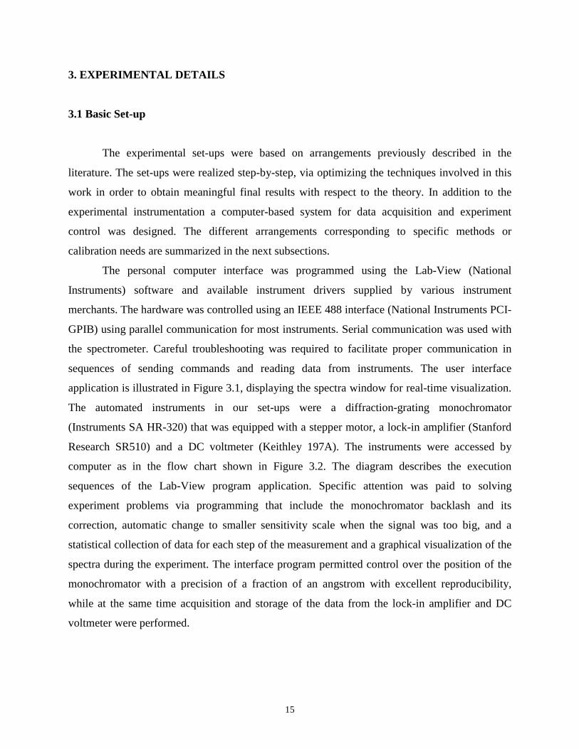
The automated instruments in our set-ups were a diffraction-grating monochromator
(Instruments SA HR-320) that was equipped with a stepper motor, a lock-in amplifier (Stanford
Research SR510) and a DC voltmeter (Keithley 197A). The instruments were accessed by
computer as in the flow chart shown in Figure 3.2. The diagram describes the execution
sequences of the Lab-View program application. Specific attention was paid to solving
experiment problems via programming that include the monochromator backlash and its
correction, automatic change to smaller sensitivity scale when the signal was too big, and a
statistical collection of data for each step of the measurement and a graphical visualization of the
spectra during the experiment. The interface program permitted control over the position of the
monochromator with a precision of a fraction of an angstrom with excellent reproducibility,
while at the same time acquisition and storage of the data from the lock-in amplifier and DC
voltmeter were performed.

16
Figure 3.1 User interface of the program for data acquisition and experiment control.
17
Figure 3.2 Flow chart for the data acquisition and experiment control program.
START, go to first wavelength
Wait three times longer than thelock-in amplifier time constant
Read ∆V (~ ∆R), the AC voltagefrom lock-in amplifier
Read V (~ R), the DC voltagefrom the voltmeter
Calculate ∆V/ V = ∆R/ R
Plot ∆R/ R versus wavelength
Store λ, ∆V, V, and ∆R/ R
More ?
Go tonext λ
Is the signaltoo large?
STOPYes No
No
Yes
DecreaseSensitivity

18
For a good accuracy in the estimation of real wavelengths corresponding to the data, the
monochromator was carefully calibrated. A mercury calibration lamp with very narrow emission
lines was used as the light source at the input of monochromator to make the correspondence
between the wavelength indicated by the instrument and the corresponding mercury lamp
wavelengths. The light from the mercury lamp was chopped to facilitate the detection of small
signals using phase sensitive detection (lock-in amplifier). The reference frequency fixed by the
chopper is also used as an input for the lock-in amplifier to detect only that AC component
having a frequency that is equal to the chopper reference frequency.
To observe the resolution provided by the use of a particular slit dimension, the detected
peaks were fitted with Gaussian functions (Figure 3.3) to obtain the full width at half maximum
(FWHM) corresponding to each slit and look at the width versus slit dependency. The
differences between true wavelengths from the mercury lamp and the monochromator dial
wavelengths are symbolized with ∆λ, and these values were calculated from the maximum peak
positions. The change in ∆λ versus the true wavelength is represented in Figure 3.4 and the data
from the fits are found the Table 3.1. Polynomial function fits were employed to estimate the ∆λ
function variation for the entire range of considered wavelengths. The monochromator
calibration furnished an accuracy of wavelength determination of about 1 Å.
3.2 Photoreflectance Set-up
We have chosen to use photoreflectance in our laboratory because it is a contactless and
nondestructive technique. The method takes advantage of the application of a small periodic
perturbation to a physical property of the sample. The change in optical function (reflectivity) is
only a small fraction of its unperturbed value, typically 1 part in 104 or less. The perturbation is
extracted through the use of a lock-in amplifier tuned to the modulation frequency.28 The
conventional photoreflectance apparatus17 uses a mechanical chopper to modulate the laser light
and is represented in Figure 3.5. The modulation of the sample is produced by photoexcitation of
electron-hole pairs created by the laser. The laser light will have a characteristic wavelength
corresponding to radiation with an energy above the band gap of the sample studied to assure
that an adequate number of electron-hole pairs are photoexcited to produce the PR signal.

19
Figure 3.3 Mercury lamp line seen at the detector as a function of horizontal slit. All curves
were rescaled for width comparison.
Wavelength (Å)
5460 5465 5470 5475 5480 5485 5490
Arb.
Units
Slit 0.1 mmSlit 0.25 mmSlit 0.5 mmSlit 1 mm

20
Figure 3.4 Monochromator calibration corresponding to different horizontal slits.
Wavelength (Å)
3000 4000 5000 6000 7000 8000 9000 10000 11000
∆ λ (Å
)
12
13
14
15
16
17
18
19
Slit 0.10 mmSlit 0.15 mmSlit 0.30 mmPolynomial fit

21
Slit(mm)
Mercury lampwavelength, λ0, (Å)
Monochromatorwavelength, λe, (Å)
∆λ = λe-λ0, (Å) FWHM, (Å)
0.5 3131.56 3147.72 17.74 5.853131.84 3148.44 17.46 4.753650.15 3665.71 15.56 5.043654.83 3668.6 13.77 5.893663.28 3679.58 16.3 8.784046.56 4063.64 17.08 6.054358.35 4375.34 16.99 4.845460.74 5476.79 16.05 4.695769.6 5786.38 16.78 4.725790.66 5807.25 16.59 4.776907.5 6923.13 15.63 4.97
4046.56 x 2 8107.3 14.2 4.544358.35 x 2 8730.52 13.82 4.58
0.3 3650.15 3667.57 17.42 3.853654.83 3672.58 17.75 3.363663.28 3680.37 17.09 3.914046.56 4064.34 17.78 3.684358.35 4376.33 17.98 3.745460.74 5477.72 16.98 3.655769.6 5786.9 17.3 3.675790.66 5807.91 17.25 3.746907.5 6923.84 16.34 4.3
3650.15 x 2 7316.02 15.72 3.514046.56 x 2 8108.25 15.15 3.54358.35 x 2 8731.11 14.41 3.71
0.25 3131.56 3147.66 16.1 2.543131.84 3148.2 16.36 2.753650.15 3666.76 16.61 2.453654.83 3671.56 16.73 2.33663.28 3679.73 16.45 2.794046.56 4063 16.44 2.354358.35 4375.17 16.82 2.375460.74 5476.72 15.98 2.355769.6 5786.1 16.5 2.335790.66 5807.1 16.44 2.37
3131.84 x 2 6278.73 15.65 2.374358.35 x 2 8730.6 13.9 2.265460.74 x 2 10933.45 11.97 3.05

22
Slit(mm)
Mercury lampwavelength, λ0, (Å)
monochromatorwavelength, λe, (Å)
∆λ = λe-λ0, (Å) FWHM, (Å)
0.15 3650.15 3667.35 17.2 1.943654.83 3671.92 17.09 1.793663.28 3680.18 16.9 2.064046.56 4063.87 17.31 2.04358.35 4375.82 17.47 1.975460.74 5477.4 16.66 1.965769.6 5786.74 17.14 1.885790.66 5807.76 17.1 1.886907.5 6923.54 16.04 1.75
3650.15 x 2 7315.72 15.42 1.794046 x 2 8108.09 14.99 1.68
4358.35 x 2 8730.98 14.28 1.675460.74 x 2 10934.48 13 1.55
0.10 3650.15 3667.4 17.25 1.43654.83 3672.02 17.19 1.213663.28 3680.46 17.18 1.654046.56 4064.3 17.74 1.394358.35 4376.31 17.96 1.315460.74 5477.48 16.74 1.265769.6 5786.8 17.2 1.35790.66 5807.83 17.17 1.36907.5 6923.6 16.1 1.32
3650.15 x 2 7315.93 15.63 1.14046 x 2 8108.13 15.03 1.1
4358.35 x 2 8731.05 14.35 1.115460.74 x 2 10933.64 12.16 1.55
Table 3.1 Mercury lamp calibration of the monochromator.

23
Figure 3.5 Schematic representation of a conventional photoreflectance experiment
arrangement (after Reference 17).

24
In addition, a monochromatic beam of light coming from the monochromator is hitting
the sample surface in the same area as the impinging laser light. The detector will collect the
reflected light from the sample that contains three components: a DC signal I0(λ)R(λ), an AC
signal proportional with the modulated reflectance I0(λ)∆R(λ) and another AC signal ∆IPL(λ) that
represents the photoluminescence (PL) signal, where R(λ) is the unperturbed reflectance of the
sample and ∆R(λ) is the modulated reflectance. Because the PL signal entering the detector will
have the same frequency as the modulated reflectance, its contribution will mix with the useful
reflectance signal acting as a constant background. One of the challenges of the PR technique is
to eliminate the PL contribution to the signal. Shen and Dutta29 proposed a sweeping
photoreflectance (SPR) technique to minimize the effect of the PL during the measurements.
Using their set-up as a model, the PR experimental set-up realized in our lab is presented in
Figure 3.6. Light from a tungsten lamp is sent to a monochromator having a focal length of 1/4 m
that will output a certain wavelength controlled via the PC interface. The output light from the
monochromator will be focused on the sample with a lens forming a narrow spot (0.5 mm width
by 6 mm height), where the modulated laser light is also focused. The laser light is incident at a
different angle to prevent its later collection in the detector used to monitor the reflected light. As
the source for the coherent light, we used a semiconductor laser diode (Philips CQL806/30)
combined with a constant power laser driver (Thorlabs LD1100) to supply the constant current.
The detector placed at the reflection angle for the probe beam was protected with a bandpass
filter to block the wavelength of scattered light corresponding to the laser wavelength. The
detector is a silicon PIN photodiode detector that sends the signal to the lock-in amplifier for the
AC signal detection and to a DC voltmeter via a V/A preamplifier (Ithaco 1641 preamplifier).
The quantity of interest in the PR technique, ∆R/R is obtained through the normalization
procedure realized by dividing I0∆R measured with the lock-in amplifier by I0R measured with
the DC voltmeter, both signals being recorded and stored at the same time with the
corresponding monochromator wavelength using the LabView data acquisition system.
In the sweeping technique, the mechanical chopper from the classical setup (Fig. 3.5) is
replaced by an acousto-optic modulator/deflector which operates in the deflection mode (Fig.
3.6). The pump beam is swept on the sample with respect to the probe beam position. During
half of its periodic oscillation, the pump beam spot will coincide with the probe beam spot to

25
Figure 3.6 Schematic representation of the photoreflectance set-up.

26
modulate the reflectance from the sample. The sweeping distance is kept smaller than the active
area of the detector and the laser intensity is kept constant. If collected properly, the PL signal
produced by the sweeping beam is seen by the detector as a DC luminescence IPL(λPL). This way
the detector will not see two-mixed AC signals but only the useful PR signal separated from the
PL contribution. Moreover, the PL elimination was useful for the increase of the relative signal-
to-noise ratio. A few experiments were done with the acousto-optic modulator working in
chopping mode to observe differences in PR signal amplitudes, but without observing any
significant changes. In the chopping modulation case the PL signal was bigger as expected.
Each component of the set-up and its influence to the final PR signal was carefully
checked and replaced if necessary. One of the components that influenced the noise in the
detection scheme is the V/A preamplifier. Two types were investigated: an Oriel preamplifier
(model 70710) and a Ithaco preamplifier (model 1641) with different amplification factors. At a
certain wavelength the photodiode was kept in the dark chamber that was used for PC
experiments without external illumination and the chopper supplied the AC reference signal.
During a time period of ~ 30 min. the AC and DC signals detected by the lock-in and voltmeter
were monitored to look at the mean value and standard deviation of the signals recorded. These
signals represent the dark, or noise, AC and DC signal. The Ithaco preamplifier was preferred
because of its higher capacity to detect AC signals for the same amplification scale while
providing lower levels of noise due to the DC background signal.
To minimize the PL contribution to the lock-in signal while the PR contribution was
increased, another set-up correction was performed by optimizing the system of lenses before the
sample and after the reflection along the probe beam path. To collect the same solid angle of
light at the detector as the one sent to the sample from the monochromator, the L1 and L2
corresponding focal numbers n1=d1/f1 and n2=d2/f2 need to be matched, where d1 and d2 are the
corresponding lens diameters, and f1 and f2 are the corresponding lens focal lengths. This
optimization was able to decrease the relative effect of the PL by almost an order of magnitude.
At the same time an adequate diameter was chosen for the L2 lens to collect the sweeping PL
generated by the laser in order to see it as a DC signal by keeping it in the active area of the
detection photodiode. To check, the initial photodiode with a square active area of 16 mm2 was
replaced with a photodiode having larger active area of 100 mm2 to see the influence on

27
minimizing the PL signal. However, a considerable improvement has not been observed with
enlarging the active area of the detector.
3.2 Photoconductivity Set-up
The potential of the spectral photoconductivity (SPC) characterization technique to study
the photoconductor properties of semiconductors and to reveal imperfection states in the band
gap16 were the arguments to apply the SPC method in our lab. In the case of the GaN samples
considered in our study, the PC signal is very small compared with the dark current. Detection of
such weak photosignals needs a careful selection of several parameters. It is necessary to know
the change in the resistance of the sample caused by incident radiation, the impedance of the
measuring circuit, the response time, the capabilities and limitations of the photodetector, and
sources of noise and their magnitudes. The combined knowledge of these factors helps in
selecting the proper instruments.26
To resolve the weak photoconductivity signal in the case of epitaxial layers of GaN we
have employed a modulation technique, using a mechanical chopper to modulate the incident
light on the sample. The schematic of the SPC experiment is shown in Figure 3.7. The output
signal is an AC signal mixed with the dark current. Even though very weak, the induced AC
photosignal can be separated by a lock-in phase sensitive amplifier, having the same frequency
as that of the chopper. The frequency of modulation of the light beam is determined in such a
way as to match the response time of the photoconductor. In the case of GaN samples the
response time was slow due to persistent photoconductivity, taking a long time to attain the
steady state photocurrent. This is why the frequency for the type of samples we studied was
chosen to be as low as possible, about 6-7 Hz. This lower limit was imposed by frequency
nonhomogenity of the chopper that is seen by the amplifier at lower frequencies. The use of an
appropriate frequency to maximize the signal needs to be done while considering at the same
time the possibility of high 1/f noise. Four contacts were made at the corners of rectangular
samples and the contacts were connected in pairs in such a way that the incident monochromatic
light was focused between the two pairs. We have used soldered indium to make ohmic contacts
on the n-type GaN. Other p-type GaN samples had Ni/Au contacts deposited on them that

28
Figure 3.7 Phase-sensitive system for photoconductivity measurement.

29
provided to be ohmic for this type of material. A load resistor was placed in series with the
photoconductor being studied. The voltage was collected either from the sample or from the
load resistor. As the voltage source we have used either a battery or a constant current source.
Both cases provide the same relation of proportionality between the light generated
photoconductivity and the voltages measured across the photoconductor as stated below.
In the case of the circuit with the battery providing a constant voltage, the photovoltage
across the sample can be determined by evaluating the difference between the voltages with and
without radiation:26
d
Ld R
RV+
=LR
V (3.1)
When the sample is illuminated the voltage is:
Ill
LIll R
RV+
=LR
V (3.2)
where Rd is the dark resistance of the sample, RIll is the illuminated sample resistance and V is
the applied voltage. The signal response is given by:
++
∆=−=∆))(( LdIllL
LdIll RRRRRVRVVV (3.3)
where ∆R = Rd – RIll.
In the case when a constant current source is used to power the circuit, the photovoltage
across the sample can be evaluated using a similar procedure to the one mentioned above.
The dark voltage is:
d
dd R
RV
+=
LRV
(3.4)
and the voltage when the sample is illuminated is:
Ill
IllIll R
RV
+=
LRV
(3.5)
Then the difference in conductance caused by the radiation is given by:
dIll RRG 11 −=∆ (3.6)
that will transform Equation 3.3 into:

30
))(( dLIllL
IlldL
RRRRGRRR
VV
++∆
=∆ (3.7)
For the case when the change in the dark resistance is small (Rd ≈ RIll) as our samples
case, the Equation 3.7 becomes:
2
2
)( dL
dL
RRGRR
VV
+∆
=∆ (3.8)
which is the same as the Equation 2.10 from Reference 26, calculated for a constant voltage
source. Equation 3.8, which assumes that the sample is illuminated uniformly, states the
proportionality between the change in conductivity and the ratio between the measured DC and
AC voltages. This equation will be applicable in case of either a constant voltage source or a
constant current source.
The value of the load resistance RL that is controlled by the user can be optimized in
order to obtain the maximum photoresponse. This will be obtained when the relation d(∆V)/dRL
= 0 is satisfied. The value for the photoresponse maximization will be RL = Rd. Thus we used
load resistors matched to our sample resistance.
Thus Equation 3.8 permits us to determine the spectral photoresponse experimentally
under the assumption that the intensity of light on the sample remains constant over the
wavelength range of the measurement, which is not a true statement for the tungsten lamp we
have used. A lamp power calibration was done to eliminate the lamp power contribution to the
photoresponse signal. For this purpose we replaced the sample circuit with a calibrated power
meter borrowed from Prof. N.C. Giles’ laboratory to measure the spectral power distribution of
the entire system including the lamp, monochromator and optics.
Another particular problem with the SPC set-up was that the diffraction grating of the
monochromator generates second order diffraction beams that are the doubled initial wavelength.
This means that the first order diffraction on the monochromator grating of the long wavelengths
are mixed together with the second order diffraction of the short wavelengths. To eliminate this
problem we have used a set of bandpass filters, one cutting any wavelength below 300 nm to
study the band gap response of the GaN samples that we measured, while for studying the states
in the band gap, the second filter was necessary to cut all wavelengths below 570 nm that
includes the second order diffraction of the short wavelengths. The two filters were considered,
including their wavelength association, when doing the power calibration. As we will see in the

31
next chapter, the power calibration influences the final SPC data and calibration curves from two
different power meters were considered in the present study.

32
4. RESULTS
4.1 Concentration determination of small amounts of Zn in Cd1-xZnxTe bulk
semiconductors using photoreflectance spectroscopy
As outlined in Section 2.1, PR spectroscopy has been demonstrated to be very effective
for accurate determination of characteristic energy levels in compound semiconductors. The
band gap energy in ternary or quaternary semiconductor compounds is dependent on the relative
concentration of the constituents. It was proposed30 that the room temperature band gap energy
of Cd1-xZnxTe compounds can be estimated using PR with an accuracy of 0.4 meV for small
concentrations of Zn (x < 0.2), leading to a precision in composition determination of about
0.001 by way of band gap energy determination. Based on these data and on the research
motivation presented in Section 1.3, the experiments presented here are focused on obtaining a
high accuracy in Cd1-xZnxTe compound concentration determination based on band gap
estimation.
The first study included a set of twelve bulk Cd1-xZnxTe samples with 0 ≤ x ≤ 0.1,
which was furnished by eV-Products, Inc. The samples were grown using the vertical Bridgeman
method and are considered to be high quality monocrystalline materials. The samples were 16 ×
16 × 1 mm3 and most of them are oriented (211) or (111). This particular set of samples was
used to obtain an estimation of the experimental precision for concentration determination. They
were then sent to ChemIcon, Inc. as standards necessary for the calibration of their imaging
technique as part of a larger, collaborative program.
The modulation of the samples to reveal the PR effect was done using a Phillips laser
diode with a wavelength of 675 nm. The energy corresponding to the emission line was above
the band gap of materials studied and the output laser power was adjustable up to 30mW. The
modulation frequency was kept at 200 Hz. On each sample, five different spots were used to map
the composition variation, four at the corners and one in the center. The wavelength ranges for
the scans corresponded to the region were the band gap transition or excitonic transition should
take place.
Various experimental parameters were optimized as described in Section 3.2 to obtain the
maximum PR signal unperturbed by other effects such as PL or Franz-Keldysh oscillations.24 To

33
avoid such perturbations and to optimize the maximum PR signal, a study of the laser output
power influence on the signal was done on several samples. Some representative PR spectra for
various laser powers are illustrated in Figure 4.1. It can be seen that with increasing the laser
power the PL background also increases, a phenomenon that is not wanted. At the same time, the
PR amplitude of the signal increases up to a laser power of 14.25 mW, and then decreases for
higher values. For the highest values of the laser power a feature is observed to the left of the
main PR transition, corresponding to smaller energies, that can be attributed to either defects or
impurities present in the material starting to contribute to the spectrum. The optimum power for
which PL is sufficiently small and no “extra” feature is present to the left while the PR signal is
maximized was chosen to be 9.5 mW. This power was used for obtaining the PR spectrum of the
entire set of eV-Products samples.
Values of Eg as a function of concentration have to be extracted from a theoretical fit.
The third derivative modulation theory presented in Section 2.1 is adequate for the experiments
considered here, and the equation used to fit the measured spectra was deduced based on
Equation 2.13:
)cos(])[(/ 2/22 ψφ mEECRR mg −×Γ+−×=∆ − (4.1)
where:
Γ+−
−= −
22
1
)(cos
g
g
EE
EEψ (4.2)
and the other parameters were explained in Section 2.1. The m value for the band gap fit is 2.5,
while for an excitonic fit m = 2, as previously outlined. The experimental data were fit to
Equation 4.1 using a non-linear least-squares fitting routine based on a modified Marquardt-
Levenberg algorithm. These fits were performed using SigmaPlot (Jandel Scientific). All
experiments were done at room temperature and an excitonic contribution to the PR signal was
expected.15, 30
An equation based on a prior study linking alloy composition with band gap30 was used
to calculate the compound concentration from the band gap value (in eV):
Eg (Cd1-xZnxTe) = Eg (CdTe) + 0.631x + 0.128x2 (4.3)

34
Figure 4.1 Output laser power influence on the photoreflectance signal for a Cd0.954Zn0.046Te
sample (8222-T3).
Energy (eV)
1.42 1.44 1.46 1.48 1.50 1.52 1.54 1.56 1.58 1.60
∆ R/R
-1e-5
0
1e-5
2e-5
3e-5
2.4 mW9.5 mW14.25 mW28.5 mW

35
The first term gives the base band gap for CdTe with the other terms giving the change in Eg
with composition. Tobin et al.30 have used an Eg for CdTe of 1.5045 eV based on an
interpretation of the PR signal as originating from a band-to-band transition. This conflicts with
analysis of this transition by Yu et al.31 and Sanchez-Almazan et al.15 For each of the two x = 0
samples, the spectra from all five spots on each sample were fitted taking into account both band
gap and excitonic effects. The exciton binding energy was fixed at 10 meV, as reported in
literature.31 The fit results can be found in Table 4.1 together with all other fit results for the eV-
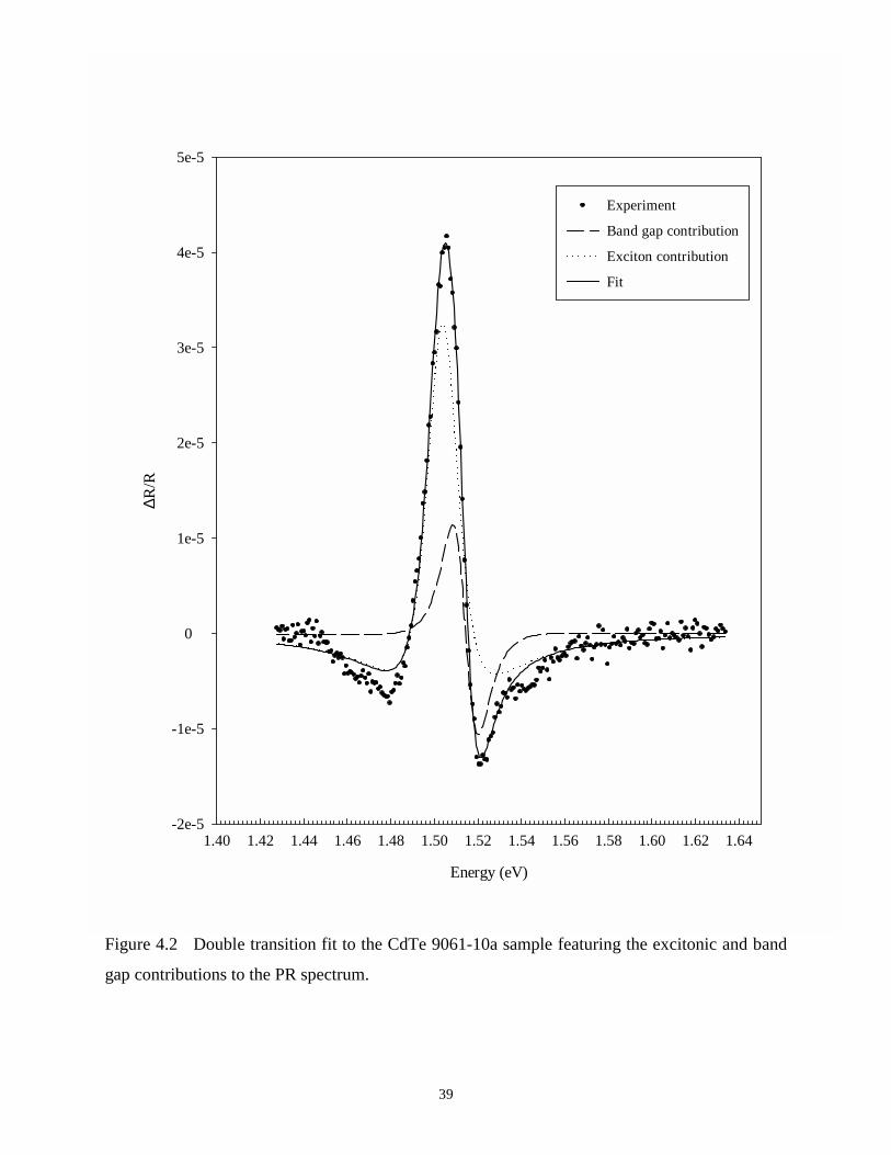
Products twelve-sample set. A typical spectra for the CdTe samples is plotted in Figure 4.2,
including the fit that adds the two relative contributions of the transitions considered. The band
gap of CdTe was calculated as the mean value of all the measurements of the two samples. The
average band gap energy was found to be 1.5145 eV, in very good agreement with the value of
1.514 eV that is reported earlier.31 The value obtained for our x = 0 samples was used as the
endpoint for the CdTe band gap energy in Equation 4.3 to compute the x-value, which resulted in
the following equation for x:
7562.58125.74648.2 −+−= gEx (4.4)
where Eg of the Cd1-xZnxTe compound is measured in eV.
Analysis of the PR spectra of the Cd1-xZnxTe samples with 0 < x < 0.1 revealed that a
single excitonic line fits the experimental results well (Figure 4.3) for the laser power chosen.
Γ broadening values resulting from the fits are below 20 meV which indicates high quality
material, so it was considered that excitonic effects are the main contribution to the PR spectra as
also suggested in other work.15 The higher quality of material is associated with the presence of
excitons and ultimately with their domination of the PR spectra. Band gap energies obtained
from the PR fit results can be found in Table 4.1. The exciton binding energy of 10 meV for
CdTe was added to the excitonic transition energies to compute Eg and determine the Zn
concentration using Equation 4.4. The maps of the concentration variation for samples with x
smaller than 0.1 are presented in Figure 4.4. Mean values for each of the sample are also
indicated. The relative order of the mean values for composition are in good agreement with
transmittance experiments on the same set of samples that was done in Professor L. Halliburton’s
laboratory. The transmittance spectra can be found in Figure 4.5, where it can be observed that
the order in composition of samples deduced from PR corresponds to the same order in
wavelengths for absorption revealed by transmittance experiments.
36
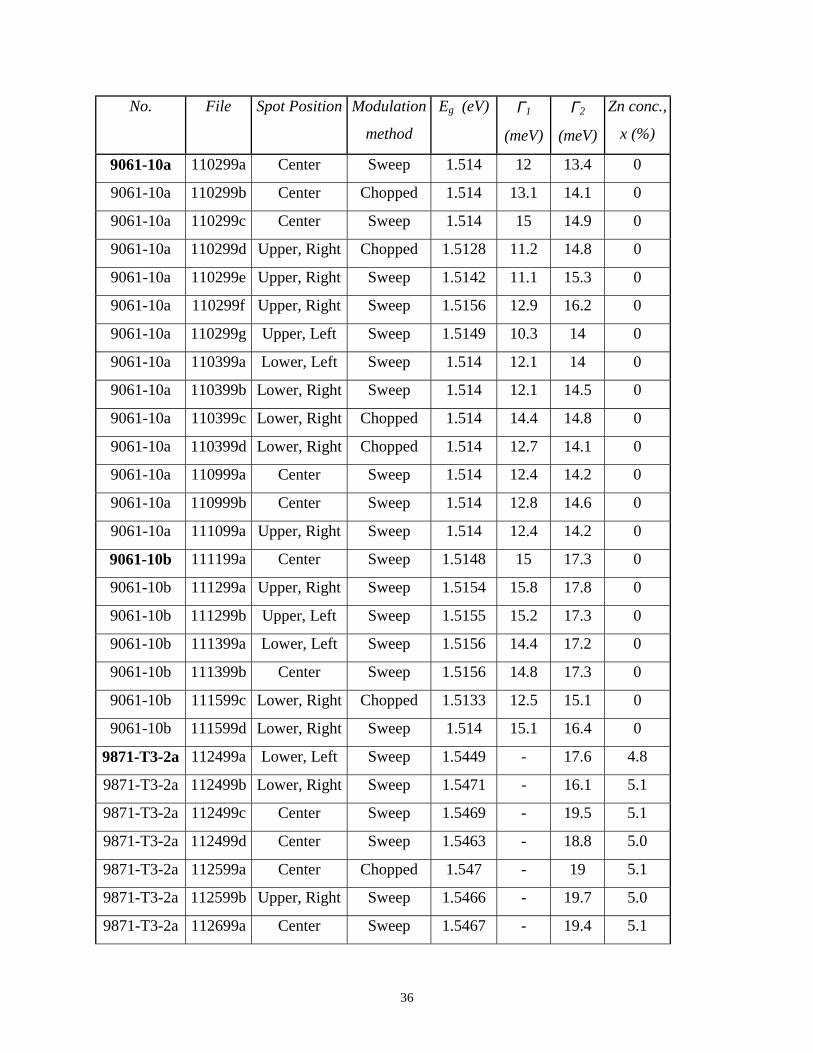
No. File Spot Position Modulation
method
Eg (eV) Γ1
(meV)
Γ2
(meV)
Zn conc.,
x (%)
9061-10a 110299a Center Sweep 1.514 12 13.4 0
9061-10a 110299b Center Chopped 1.514 13.1 14.1 0
9061-10a 110299c Center Sweep 1.514 15 14.9 0
9061-10a 110299d Upper, Right Chopped 1.5128 11.2 14.8 0
9061-10a 110299e Upper, Right Sweep 1.5142 11.1 15.3 0
9061-10a 110299f Upper, Right Sweep 1.5156 12.9 16.2 0
9061-10a 110299g Upper, Left Sweep 1.5149 10.3 14 0
9061-10a 110399a Lower, Left Sweep 1.514 12.1 14 0
9061-10a 110399b Lower, Right Sweep 1.514 12.1 14.5 0
9061-10a 110399c Lower, Right Chopped 1.514 14.4 14.8 0
9061-10a 110399d Lower, Right Chopped 1.514 12.7 14.1 0
9061-10a 110999a Center Sweep 1.514 12.4 14.2 0
9061-10a 110999b Center Sweep 1.514 12.8 14.6 0
9061-10a 111099a Upper, Right Sweep 1.514 12.4 14.2 0
9061-10b 111199a Center Sweep 1.5148 15 17.3 0
9061-10b 111299a Upper, Right Sweep 1.5154 15.8 17.8 0
9061-10b 111299b Upper, Left Sweep 1.5155 15.2 17.3 0
9061-10b 111399a Lower, Left Sweep 1.5156 14.4 17.2 0
9061-10b 111399b Center Sweep 1.5156 14.8 17.3 0
9061-10b 111599c Lower, Right Chopped 1.5133 12.5 15.1 0
9061-10b 111599d Lower, Right Sweep 1.514 15.1 16.4 0
9871-T3-2a 112499a Lower, Left Sweep 1.5449 - 17.6 4.8
9871-T3-2a 112499b Lower, Right Sweep 1.5471 - 16.1 5.1
9871-T3-2a 112499c Center Sweep 1.5469 - 19.5 5.1
9871-T3-2a 112499d Center Sweep 1.5463 - 18.8 5.0
9871-T3-2a 112599a Center Chopped 1.547 - 19 5.1
9871-T3-2a 112599b Upper, Right Sweep 1.5466 - 19.7 5.0
9871-T3-2a 112699a Center Sweep 1.5467 - 19.4 5.1

37
No. File Spot Position Modulation
method
Eg (eV) Γ1
(meV)
Γ2
(meV)
Zn conc.,
x (%)
10118-3a 112799a Center Sweep 1.5316 - 14.5 2.7
10118-3a 117799b Upper, Right Sweep 1.5312 - 15 2.6
10118-3a 112799c Upper, Left Sweep 1.5313 - 14.6 2.7
10118-3a 112899a Lower, Left Sweep 1.5317 - 14.6 2.7
10118-3a 112899b Lower, Right Sweep 1.5316 - 14.7 2.7
9759-19a 112999a Center Sweep 1.5254 - 14.4 1.7
9759-19a 112999b Upper, right Sweep 1.5254 - 15.3 1.7
9759-19a 112999c Upper, Left Sweep 1.5252 - 14.4 1.7
9759-19a 120799a Lower, Left Sweep 1.5252 - 14.8 1.7
9759-19a 120799b Lower, Right Sweep 1.5248 - 14.4 1.6
9759-19a 120899a Center Sweep 1.5252 - 14.5 1.7
10118-4b 120299a Center Sweep 1.5344 - 10.3 3.1
10118-4b 121099a Upper, Right Sweep 1.5356 - 11.4 3.3
10118-4b 121099b Upper, Left Sweep 1.5348 - 9.3 3.2
10118-4b 121699a Lower, Left Sweep 1.5345 - 9.9 3.2
10118-4b 121699b Lower, Right Sweep 1.5352 - 10.5 3.3
10118-4b 121799a Center Sweep 1.535 - 10.3 3.2
9478-c3-18c 121999a Center Sweep 1.5429 - 14.4 4.5
9478-c3-18c 121999b Upper, Left Sweep 1.5438 - 14.2 4.6
9478-c3-18c 122199a Upper, Right Sweep 1.5441 - 15.4 4.7
9478-c3-18c 122199b Upper, Right Sweep 1.5451 - 15.2 4.8
9478-c3-18c 010200a Lower, Right Sweep 1.5441 - 14.5 4.7
9478-c3-18c 010200b Lower, Left Sweep 1.5433 - 14.4 4.5
9038-H3-7 012300c Upper, Right Sweep 1.5329 - 17.8 2.9
9038-H3-8 012300d Upper, Left Sweep 1.5302 - 13.3 2.5
9038-H3-10 012300e Lower, Left Sweep 1.5305 - 14.8 2.5
9038-H3-11 012400b Lower, Right Sweep 1.5309 - 14.5 2.6
9038-H3-11 012400c Center Sweep 1.5302 - 14.8 2.5

38
No. File Spot Position Modulation
method
Eg (eV) Γ1
(meV)
Γ2
(meV)
Zn conc.,
x (%)
10118-3 012700a Upper, Right Sweep 1.5326 - 14.8 2.9
10118-3 012800a Upper, Left Sweep 1.5327 - 15.1 2.9
10118-3 012800b Lower, Left Sweep 1.5323 - 15.2 2.8
10118-4 012800c Lower, Right Sweep 1.5322 - 15.2 2.8
10118-3 013100a Center Sweep 1.533 - 14 2.9
9478-C3-18 020100a Upper, Right Sweep 1.5443 - 14.6 4.7
9478-C3-18 020200a Center Sweep 1.544 - 14 4.6
9478-C3-18 020300a Upper, Left Sweep 1.5435 - 14.4 4.6
9478-C3-18 020300b Lower, Left Sweep 1.5427 - 15.2 4.4
9478-C3-18 020400a Lower, Right Sweep 1.5444 - 14.9 4.7
9478-C3-18 020400b Center Sweep 1.5431 - 14.2 4.5
8222-T3 102299a Upper, Right Sweep 1.5445 23.1 14.1 4.7
8222-T3 102299c Upper, Left Sweep 1.5444 23.5 14.2 4.7
8222-T3 102599a Lower, Right Sweep 1.5452 22.7 14.5 4.8
8222-T3 102799a Center Sweep 1.5433 23 14.1 4.5
8222-T3 102799c Upper, Right Sweep 1.5434 22 13.8 4.5
8222-T3 102799c Upper, Right Sweep 1.5429 - 14.4 4.5
8222-T3 102799d Upper, Right Chopped 1.5433 22.6 13.9 4.5
8222-T3 102799d Upper, Right Chopped 1.5428 - 14.2 4.4
A57-18b 050900f Center Sweep 1.5790 8.2 11.2 10.0
A57-18c 051000b Center Sweep 1.5785 8.1 11 10.0
Table 4.1 Results of fitting the PR spectra for the eV-Products samples obtained using an output
laser power of 9.5 mW. Γ1 and Γ2 represent the broadening parameters for band gap transition
and excitonic transition, respectively.
39
Figure 4.2 Double transition fit to the CdTe 9061-10a sample featuring the excitonic and band
gap contributions to the PR spectrum.
Energy (eV)
1.40 1.42 1.44 1.46 1.48 1.50 1.52 1.54 1.56 1.58 1.60 1.62 1.64
∆R/R
-2e-5
-1e-5
0
1e-5
2e-5
3e-5
4e-5
5e-5
Experiment
Band gap contribution
Exciton contribution
Fit

40
Figure 4.3 Representative PR spectra for all Cd1-xZnxTe eV-Products samples with x < 0.1,
including the single excitonic transition fit (this is sample 9478-C3-18c with x = 0.046).
Energy (eV)
1.40 1.42 1.44 1.46 1.48 1.50 1.52 1.54 1.56 1.58 1.60 1.62 1.64
∆R/R
-2e-5
-1e-5
0
1e-5
2e-5
3e-5
4e-5
ExperimentExciton fit

41
Figure 4.4 Compositional variation on the surface of the eV-Products Cd1-xZnxTe samples with
0 < x < 0.1.
1.7 %
1.6 %
1.7 %
1.7 %
1.7 % 2.9 %
2.8 %
2.9 %
2.8 %
2.9 % 2.6 %
2.7 %
2.7 %
2.7 %
2.7 % 3.3 %
3.3 %
3.2 %
3.2 %
3.1 %
5.0 %
5.1 % 4.8 %
5.1 % 4.7 %
4.7 %
4.6 %
4.4 %
4.6 % 2.9 %
2.6 %
2.5 %
2.5 %
2.5 % 4.7 %
4.7 %
4.6 %
4.5 %
4.5 %
9759-19a xmean = 1.7 %
10118-3xmean = 2.9 %
10118-3a xmean = 2.7 %
10118-4b xmean = 3.2 %
9871-T3-2a xmean = 5.0 %
9478-C3-18 xmean = 4.6 %
9038-H3-7 xmean = 2.6 %
9478-C3-18cxmean = 4.6 %

42
Figure 4.5 Experimental transmittance data for the eV-Products sample set. In parenthesis are
the calculated Zn concentrations from PR fits and the values furnished by eV-Products,
respectively.
Wavelength (nm)
800 820 840 860 880 900
Tran
smitt
ance
(%)
0.1
1
10
100
9478-C3-18C (4.6/4.0)10118-3(2.9/2.4) 9038-H3-7 (2.6/4.0)9061-10B (0/0)9759-19A (1.7/1.2)10118-4B (3.2/2.4)9871-T3-2A (5.0/4.0)9478-C3-18 (4.6/4.0)10118-3A (2.7/2.4)9061-10A (0/0)A57-18B (10.0/10.0)A57-18C (10.0/10.0)

43
The eV-Products samples supposed to have 10 % of Zn in composition cannot be fitted
with excitonic line shape only and again the double contribution transition fit was used with the
excitonic contribution being dominant. The calculated relative Zn concentrations from the band
gap energy are 10.0 %, which is exactly the same as the ones provided by the crystal growers. A
PR spectrum is represented in Figure 4.6. Both the two transitions fit and the excitonic only fit
are plotted. The two-transition fit is better despite the other imperfections of the spectra that can
be found at higher and lower energies than the transition. To the right of the PR transition the
Franz-Keldysh oscillations can be observed which could not be reduced by lowering the laser
power. This is considered to be an indication that this oscillation effect is not dependent on the
intensity of the laser light but on the strength of the built-in surface electric field. This indicates
that we are in the high field regime, which requires a more complicated analysis. The feature at
lower energies that is not well fit is believed to correspond to the perturbation of the excitonic
transition, and its contribution can be reduced by laser power adjustment.
The estimation of error in the concentration determination is a delicate matter and will
depend more on the accuracy of the model used to fit the PR spectra than on experiment
uncertainties and the reproducibility of the data. The experimental reproducibility was studied
using both sweeping and chopping PR techniques and sample measurement repetition. The
experimental measurement uncertainties are small when compared with the fit issues. It is
supposed that the value for the band gap energy providing the composition will be determined
more accurately if the spectrum exhibits only one transition. In this case better precision in the
determination of the band gap energy can be obtained since the number of fitting parameters is
smaller and their values can be more easily controlled by physics theory. Once the uncertainty of

44
the band gap determination is known, the uncertainty in composition determination can be
calculated using Equation 4.4.
Another poorer quality material was considered in the PR analyses of the Cd1-xZnxTe
composition determination. The area of the sample was 11 × 9 × 0.3 cm3 but the sample was
broken into four smaller pieces. Figure 4.7 shows the sample, including the composition
mapping done by using the PR method. Table 4.2 contains the PR parameters obtained from the
fits. For most of the experimental spectra obtained on the surface of this sample the double
transition is easily distinguished as illustrated in Figure 4.8. However, a particular region of the

45
Figure 4.6 A typical PR spectrum and its fit attempts for the case of 10 % Zn eV-Products
samples (sample A57-18c).
Energy (eV)
1.46 1.48 1.50 1.52 1.54 1.56 1.58 1.60 1.62 1.64 1.66 1.68 1.70
∆R/R
-0.00015
-0.00010
-0.00005
0.00000
0.00005
0.00010
0.00015
ExperimentTwo transition fitExciton fit

46
Figure 4.7 A large (11 × 9 × 0.3 cm3) Cd1-xZnxTe sample, mapped in composition along its
surface using the PR technique. Exciton only fits are indicated.
4.3 % 4.2 %
3.9 % 4.4 %
3.7 % 4.1 %
4.0 %
4.7 % (double fit)
4.3 %
4.5 % (exciton fit)
4.4 % (exciton fit)
5.0 % (double fit)
3.2 %
3.2 %
3.1 %
3.7 %
3.8 % 3.3 %
3.2 %
4.7 % (exciton fit)
black
red
red
yellow
blue

47
No. Fragment Spot Position Imaging
Colors
Eg (eV) Γ1
(meV)
Γ2
(meV)
Zn conc.,
X (%)
010300d 4 lower yellow 1.5403 12.2 15.2 4.1
010400a 4 center - right yellow 1.5396 19.5 15.8 4.0
010400b 4 center - right yellow 1.5399 14.3 16.7 4.1
010500a 4 center - right yellow 1.5388 13.7 14.6 3.9
010600b 4 center - left yellow 1.5440 20.5 18.8 4.7
010600b 4 center - left yellow 1.5420 - 18.6 4.4
011200a 4 upper yellow 1.5430 - 23.0 4.5
011100a 4 center yellow 1.5416 21.4 17.5 4.3
011500b 3 upper blue 1.5461 25.3 18.6 5.0
011500b 3 upper blue 1.5440 - 18.8 4.7
011700a 2 right - edge red, black 1.5422 17.8 16.8 4.4
011700b 2 center red 1.5378 13.3 15.6 3.7
011800a 2 left - edge red 1.5343 13.5 15.7 3.2
011900c 2 lower black 1.5414 17.7 15.1 4.3
012200a 1 upper - left red, black 1.5379 14.5 15.4 3.7
012200b 1 upper - right red 1.5385 15.9 15.3 3.8
012300a 1 lower red 1.5346 13.2 16.0 3.2
012300b 1 center-right red 1.5352 12.0 16.2 3.3
Table 4.2 PR fit results for the large (11×9×0.3 cm3) Cd1-xZnxTe sample corresponding to
different spots on the sample.

48
Figure 4.8 Typical double transition PR spectrum and fit for large (11×9×0.3 cm3) Cd1-xZnxTe
sample, featuring the excitonic and band gap contributions to the fit.
Energy (eV)
1.40 1.45 1.50 1.55 1.60 1.65
∆R/R
-2e-5
-1e-5
0
1e-5
2e-5
3e-5
ExperimentFitBandgap contributionExciton contribution

49
sample (the upper–right portion in Fig. 4.7) is observed to provide spectra that are believed to be
only excitonic in nature. One of these spectra and its fit can be found in Figure 4.9. Taking into
account the large area of the sample and supposing that inhomogeneities can easily occur, it is
believed that this region contains higher quality material. The explanation for this effect can be
attributed to a better local polishing resulting in a smoother surface or to sample growth issues
such as an optimized growth for that particular region.
4.2 Photoconductivity spectroscopy studies of epitaxially grown GaN using various growth
methods
The defect states in the forbidden gap of GaN are usually studied by luminescence
measurements giving information about the defect state participating in the radiative
recombination processes. Spectral photoconductivity (SPC) analysis can provide valuable
information about the defect or impurity states and also the near band edge transitions
participating in the absorption of light. Moreover, the SPC technique is capable of extracting
useful information about the defect/impurity density of state distribution in the band gap.32
A set of GaN samples grown by rf-plasma MBE in our lab on sapphire substrates was
selected for the SPC experiments. The samples were squares of 13 × 13 mm2 and the epitaxially-
grown GaN layers were typically a few µm thick. Thickness values for each sample from
transmittance experiments can be found in Table 4.3. These samples exhibit a wide range of
optical and electrical properties as can be observed in the same table. All of the samples have n-
type conductivity and are unintentionally doped.33 Several of the samples were of high electrical
and structural quality, as indicated by their high mobility and low carrier concentration.
Persistent photoconductivity (PPC) effects were observed in these samples and the analyses of
the PPC data can be found in a prior publication.34 The reflectance and transmittance
measurements were done in Prof. L.E. Halliburton lab and the photoluminescence experiments in
Prof. N.C. Giles lab.
To obtain the material spectral photoresponse when using the experimental set-up
described in Section 3.2, it is necessary to divide the ratio of the measured DC and AC voltages
by the spectral power distribution of the light that is used to excite the sample.
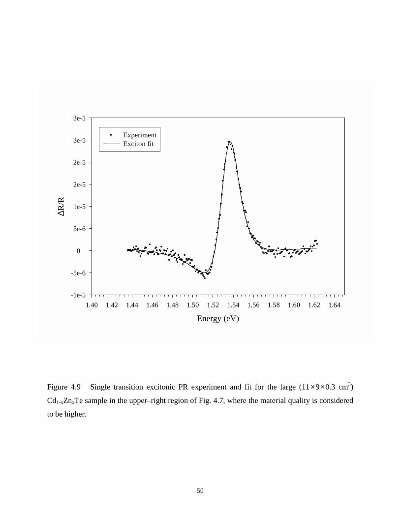
50
Figure 4.9 Single transition excitonic PR experiment and fit for the large (11×9×0.3 cm3)
Cd1-xZnxTe sample in the upper–right region of Fig. 4.7, where the material quality is considered
to be higher.
Energy (eV)1.40 1.42 1.44 1.46 1.48 1.50 1.52 1.54 1.56 1.58 1.60 1.62 1.64
∆R/R
-1e-5
-5e-6
0
5e-6
1e-5
2e-5
2e-5
3e-5
3e-5
ExperimentExciton fit

51
Sample(Thickness)
(µm)
ττττ50%
ττττ10%(s)
ττττshort(10-3 s)
a-Hduringgrowth
YellowPL
Mobility(cm2/Vs)
NConc.
(1016cm-3)
Excitonin RT
Reflectance
9824(9.2)
4.0246
0.7 weak 202 1.7 yesstrong
9821(2.0)
4.8622
0.5 weak 15 9.2 no
9826(7.5)
5.14,044
1.2 weak 9.0 1.8 yes
9825(2.6)
7.07,171
1.4 N.D. 12 1.7 yes
9910(1.72)
1329,521
1.2 weak 330 0.10 yes
9671(1.0)
646,704
2.3 yes moderate 120 77 no
9730(0.98)
21421,061
2.3 yes N.D. 4 7.2 no
9710(0.85)
29332,564
1.8 yes weak 50 85 no
9823(2.1)
3088,703
1.6 yes weak 232 140 yes
9822(2.1)
35752,922
1.0 moderate 13 0.67 (?)
Table 4.3 Various properties of some GaN samples grown by rf-plasma MBE included in this
investigation.

52
Therefore, the influence of the spectral power calibration on the final photoresponse curves was
carefully considered. Figure 4.10 illustrates the power variation versus energy corresponding to
the radiation used to photoexcite the samples. The two curves correspond to two different power
meters and slightly different optical alignments used to perform the same experiment. In the
lower energy range we can observe two main peaks, with the lower energy peak corresponding
to the maximum intensity light emission from the lamp and the higher energy peak resulting
from the blaze of the diffraction grating of the monochromator. It can be observed that the
relative ratio of the two main peaks is changed for the two curves with the lower energy peak
intensity larger in the case of the second power calibration curve. This phenomenon that can be
explained by a combination of the replacement of the tungsten lamp bulb and the optimization
process to maximize the lamp image on the monochromator diffraction grating. More
importantly, the second power meter was a newer model (Coherent, Laser Mate-QTM) than the
first (Coherent, model 212) with a vastly improved spectral sensitivity correction factor. Note
that the kinks observed at energies > 3 eV on the first power meter curve are eliminated by the
better correction of the sensitivity factor in the case of second power meter. This precludes these
artifacts from being interpreted as a feature in measured SPC spectrum.
First, the samples from Table 4.3 were measured in the SPC setup using the first power
calibration curve and a 9 V battery as a constant voltage source to collect the photoexcited
carriers. Some of the samples (9730, 9710, 9823, 9822) had a too small signal to noise ratio for
performing the SPC measurement. Equation 2.13 corrected for the incident photon flux was used
to calculate the photoconductance signal variation as a function of energy of the incident light:
∆G (hν) ~ ∆V/V/P (4.5)
where P is the incident power, hν is the energy of the incident light, and the other parameters are
explained in Section 3.2. The photoresponse curves are shown in Figure 4.11 and the spectra
were normalized to the photoresponse above the band gap of GaN, but they were not normalized
for the sample thickness. Samples 9826 and 9824 were significantly thicker than the others (7.5
and 9.2 µm vs 1 to 2 µm), which resulted in a much stronger below-gap signal.
The proposed SPC study tried to reveal defect or impurity-related states in the band gap
participating in photoconductive processes, below the band edge transition. A discussion of the
SPC data obtained on the samples from Table 4.3 can be found elsewhere.34

53
Figure 4.10 Power calibration curves for two and experimental set-ups. The inset represents the
same result on a log scale. Power meter 1 corresponds to Coherent model 212 and power meter 2
to Coherent Laser Mate-QTM.
Energy (eV)
1.0 1.2 1.4 1.6 1.8 2.0 2.2 2.4 2.6 2.8 3.0 3.2 3.4 3.6 3.8
Arb
. Uni
ts
0
1
Power meter 1Power meter 2
Energy (eV)
1.0 1.5 2.0 2.5 3.0 3.5 4.0
Log
scal
e, a
rb. u
nits
0.001
0.01
0.1
1

54
Figure 4.11 Spectral photoconductivity responses for selected GaN samples grown by rf-plasma
MBE in our lab. The sample thickness is shown in parentheses. The inset is a close-up of the
near band gap region. The Fx is the free exciton energy and Eg is the band gap energy.
Energy (eV)
1.0 1.5 2.0 2.5 3.0 3.5
Nor
mal
ized
Pho
toco
nduc
tanc
e
10-5
10-4
10-3
10-2
10-1
100 9671 (1 µm)9821 (2 µm)9822 (2.1 µm)9824 (9.2 µm)9825 (2.6 µm)9826 (7.5 µm)9910 (1.7 µm)
3.1 3.2 3.3 3.4 3.510-4
10-3
10-2
10-1
100
EgFx
3.1 eV
2.1 eV1.9 eV

55
Initially, we were trying to interpret some PC onset features that can be distinguished in case of
samples 9826 and 9824. However, using the second, improved power calibration and repeating
the measurements on sample 9824 we did not observe these particular features. A comparison
between two separate measurements of the same sample (9824) that use the power calibration
curves appropriate to the particular set-up but with the first using the original power meter and
calibration and the second the newer power meter and calibration is represented in Figure 4.12. It
can be seen that features present in the earlier experiment at 1.92 eV and 2.15 eV in the below
band gap region are removed in the later experiment and were apparently experimental artifacts.
In this study, we cannot distinguish any definite features in SPC spectra below the band edge that
could be related with exact energetic levels of impurities or defects. However, we still can get
important information about the defect states by looking at the shape of the photoresponse
spectra in the sub-band gap region. It can be see that the photoresponse starts to build up with an
onset somewhere below 1.2 eV. We cannot say where because of our set–up wavelength limits.
The increase continues monotonically until another sharp transition starts at about 3.09 eV,
which corresponds to near band edge transitions. This type of photoresponse in n-type
conducting materials can be interpreted using the model for the defect/impurity density of states
distribution in the semiconductor band gap suggested by Qiu et al.32 that is illustrated in Figure
4.13. The existence of two band tails is proposed, one that is abrupt and close to the band edges
and a gradual tail deeper into the gap. The abrupt tail revealed by the sharply stepped
photoresponse near the band edge may reflect the usual Urbach edge, while the deep gradual tail
is tentatively attributed to defect states.
Another important feature of the photoresponse spectra represented in Figure 4.11 is the
apparent resonance peak centered at 3.39 eV, observed for the case of the thicker samples 9824
and 9826. Since the free exciton binding energy in GaN is 26-28 meV35, which is about the same
as the thermal activation energy at room temperature (kBT ≈ 25.5 meV), then excitonic
contribution is expected in absorption-emission processes at room temperature. The reflectance
and photoluminescence experimental data confirm its presence at room temperature as shown in
Figure 4.14 (a) and (b) with a transition energy of about 3.415 eV. Based on these experimental
data and on a room temperature study of excitons in photoconductivity spectra,36 it was expected
that the exciton would contribute to the SPC signal.

56
Figure 4.12 Effect of the power calibration on the spectral photoresponse curve of sample 9824.
Energy (eV)
1.2 1.4 1.6 1.8 2.0 2.2 2.4 2.6 2.8 3.0 3.2 3.4 3.6 3.8
Nor
mal
ized
Pho
toco
nduc
tanc
e
0.001
0.01
0.1
1Power calibration 1Power calibration 2
Experimental Artifacts

57
Figure 4.13 Schematic distribution of states available for optical transitions in n-type GaN. The
states between Ec and Ev are assumed to be localized states. The arrow represents schematically
an optical transition for sub-band gap light absorption.

58
Figure 4.14 Room temperature reflectance (a) and photoluminescence (b) showing excitonic
transitions on MBE GaN samples (9824 and 9826, respectively)
Energy (eV) (a)
3.2 3.3 3.4 3.5 3.6
Ref
lect
ance
GaN 9824
3.415 eV
(b)

59
However, the 3.39 eV peak from our SPC spectra is too low in energy to be an excitonic
transition and is thus suspected to be related to an unidentified “impurity” rather than to an
excitonic transition. The other thinner samples do not exhibit the feature at 3.39 eV and their
photoresponse signal saturates at the value of the excitonic transition.
Another SPC study was done to observe the effect of Mg doping of GaN on the
photoresponse spectra. This time the MBE epilayer was grown on top of GaN samples that were
previously grown by metal-organic chemical vapor deposition (MOCVD) and were furnished by
Xerox-PARC. The MOCVD layers grown on sapphire substrates were n-type conducting and
were unintentionally doped during the growth. Sample 9975 is a MBE-grown undoped layer on
the MOCVD (B1410) substrate and the SPC experiment was done before and after the MBE
growth process. Results are represented in Figure 4.15, showing that the initial peak present at
3.418 eV in the SPC spectrum of the B1410 sample is shifted to 3.409 eV by the growth of the
MBE layer on top. A similar sample, but this time Mg doped GaN (9979), was also grown on
MOCVD GaN (B1647). The SPC signal response is somewhat similar to the previous case: the
saturation PC point of 3.408 eV for the B1647 sample is shifted to the lower energy of 3.394 eV
by the contribution of the Mg doped GaN top layer (Figure 4.16). This is the same energy for the
transition revealed in samples 9824 and 9826, suggesting that we have introduced the same type
of impurity when growing sample 9979 as in the case of growing samples 9824 and 9826.
Interestingly, the intensity of the resonance peak for the Mg doped sample is the most intense
from those measured in our lab, suggesting that the impurity contribution is stronger.
Finally, two hydride vapor phase epitaxy (HVPE) samples were measured in the SPC set-
up. Comparison of the two samples, LH 1089 and LH 735 featuring the near band edge peak and
MBE grown 9910 and 9824, one without and the other with peak. It is observed that one HVPE
sample (LH 1089) has the PC saturation point at the band gap energy but the other saturates at
the same energy corresponding to the excitonic transition as our sample 9910. In addition,
sample LH 735 starts to build up a feature in its shape at about the same energy as the peak of
sample 9824.
At this point, the interpretation of the near band edge transitions is not very conclusive,
but it can be noted that specific transitions that correspond to different growth conditions can be
measured providing particular energy values. The set of samples listed in Table 4.3 exhibit either
a resonance peak in SPC at 3.39 eV or a SPC saturation point corresponding to the excitonic

60
Figure 4.15 SPC response comparison of the MOCVD grown GaN and the MBE grown GaN
on top of it.
Energy (eV)
3.0 3.1 3.2 3.3 3.4 3.5 3.6 3.7 3.8
Nor
mal
ized
Pho
toco
nduc
tanc
e
0.01
0.1
1
MOCVD grown GaN substrate (B1410) Undoped MBE grown GaN (9975)
3.409 eV 3.418 eV

61
Figure 4.16 SPC response comparison of the MOCVD grown GaN and the Mg doped MBE
grown GaN on top of it.
Energy (eV)
3.0 3.1 3.2 3.3 3.4 3.5 3.6 3.7
Nor
mal
ized
Pho
toco
nduc
tanc
e
0.001
0.01
0.1
1
10
MOCVD GaN substrate (B1647)MBE Mg doped GaN (9979)
3.394 eV
3.408 eV

62
Figure 4.17 Photoconductivity spectra comparison for HVPE and MBE grown GaN. The
thickness of each sample can be found in parentheses.
Energy (eV)
3.0 3.1 3.2 3.3 3.4 3.5
Nor
mal
ized
Pho
toco
nduc
tanc
e
0.01
0.1
1
3.39 eV Fx=3.412 eV
Eg=3.438 eV
GaN - HVPE LH 1089 (1.23 mm)GaN - HVPE LH 735 (15.4 mm)GaN - MBE 9824 (9.2 mm)GaN - MBE 9910 (1.72 mm)

63
transition energy. In the case of the MBE samples grown on MOCVD GaN substrates, the initial
MOCVD sample PC saturation point or the resonance peak that is close to the excitonic energy is
shifted to lower energies toward the 3.39 eV level by the contribution of the MBE layer. This
type of phenomenon could be explained by assuming that MBE growth systematically introduces
some unwanted “impurity” seen in SPC spectra. The same type of impurity may be present in the
LH 735 HVPE sample that starts to build up a feature at an energy between 3.3 and 3.4 eV.
Future complementary photoluminescence studies may help to explain the “peak” effects that
were observed in this work.
The use of the constant current source to supply the voltage to the sample studied by SPC
helped to improve the signal to noise ratio in some of the samples. Two samples measured
initially with the battery as a voltage source that had noisy responses in the sub-band energy
region were measured again with the constant current source, this time exhibiting nice
interference effects with the light reflected from the sapphire substrate. The results are shown in
Figure 4.18. Analysis of the interference patterns using refraction indices from literature
determined the sample thickness. For 9821 a thickness of 1.87 µm and for 9910 a thickness of
1.92 µm were obtained. These values are in agreement with the values obtained by transmittance
measurements that are used to find the sample thickness and can be found in Table 4.3.
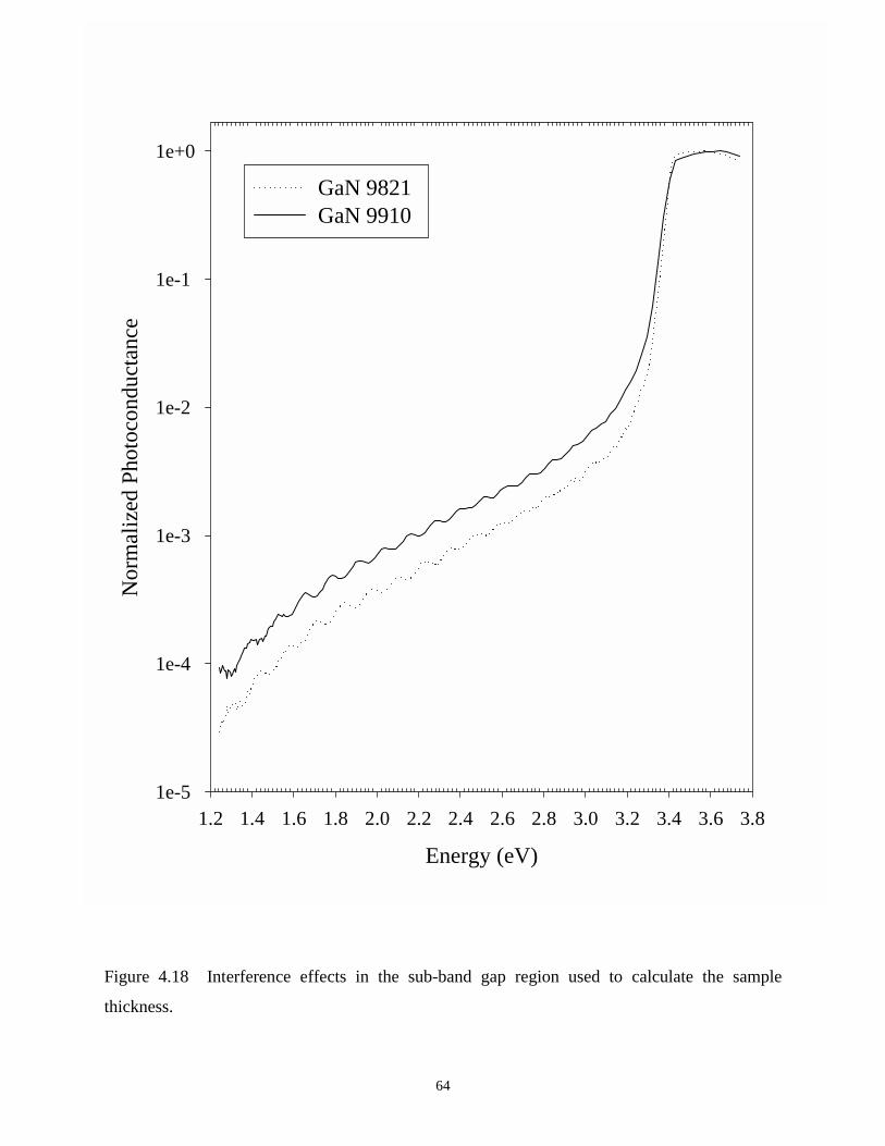
64
Figure 4.18 Interference effects in the sub-band gap region used to calculate the sample
thickness.
Energy (eV)
1.2 1.4 1.6 1.8 2.0 2.2 2.4 2.6 2.8 3.0 3.2 3.4 3.6 3.8
Nor
mal
ized
Pho
toco
nduc
tanc
e
1e-5
1e-4
1e-3
1e-2
1e-1
1e+0
GaN 9821 GaN 9910

65
5. Summary and suggested future research
Progress in compound semiconductor growth technologies is made continuously with the
demand to produce high quality materials, control their composition and move forward to
produce applications. Two types of compound semiconductor materials were considered in this
study: the ternary bulk Cd1-xZnxTe system and the epitaxial GaN system. In the case of Cd1-
xZnxTe, material it is important to achieve fine control over its composition to provide lattice-
matched substrates for the growth of Hg1-xCdxTe, which is important for infrared detection. In
the other case, the lack of lattice matched substrates for the growth of epitaxial GaN still
provides material with considerable defect densities despite the substantial amount of research on
this material date. The optical characterization techniques that were used in the present work
represent powerful tools for investigating material issues. Photoreflectance spectroscopy can
make accurate composition determinations of Cd1-xZnxTe via energy level determination, and
photoconductivity spectroscopy can be used to study defects and imperfections in the band gap
of GaN. To build the experimental set-ups for these two techniques and apply them to the
materials of interest were the principal objectives that motivated this research. The results
obtained demonstrate that the objectives were successfully accomplished.
Optimization of the experiment set-ups conditions to provide maximum responses in the
PR and PC spectra was accomplished by considering each component of the experimental
arrangement and its influence on the spectra. The aim of minimizing instrumental perturbations
to the measured spectra was attained by making successive measurements and varying conditions
for one set-up component at a time. In this way, it was assured that the observed spectra were
providing only physical information about the sample under study and not experimental
uncertainties.
After refinement the PR set-up allowed the measurement of high resolution, repeatable
spectra. The band gap energy was accurately determined considering either excitonic or
excitonic and band gap contributions to the photoreflectance spectra. Consecutively, the
composition of Cd1-xZnxTe compounds was determined using the band gap energy values. It is
concluded that the main uncertainty of the band gap determination is the fitting procedure when
using a double transition contribution, which has a large number of fitting parameters that are not
easily controlled. Further studies can optimize the PR spectra for obtaining only excitonic

66
contributions that are easier to control in the fitting procedure and obtain accurate band gap
energy data more easily. This might be possible through the use of an adequate laser power for
each sample as some preliminary results have revealed. To understand the effect of the laser on
the built-in surface electric field and make quantitative evaluations about its strength and/or
interaction with the laser incident radiation, future studies may focus on the Franz-Keldysh
oscillations.24 Complementary optical characterization techniques such as photoluminescence at
room temperature may confirm the assumption that in the case of the samples considered the
excitonic contribution is the dominant one.
Spectral photoconductivity was successfully used to study transitions near the band edge
of epitaxial layers of GaN, obtained by various growth methods. It is observed that in the case of
photoconductivity studies, further progress can be made by using a real time monitoring of the
intensity of the incident light on the sample, eliminating the uncertainties related to the influence
of the power calibration. Another set-up change can be attempted to surpass the difficulty of
measuring samples with small signal to noise ratio by using a sample electrical circuit similar to
the one described in Reference 26, page 48. To make quantitative comparisons between various
measured samples, future experiments need to take into account the sample thickness to
normalize the photoconductance spectra.

67
References
1. J.-Y. Duboz, Phys. Stat. Sol. (a) 176 (5), 5 (1999).
2. H. Morkoc, S. Strite, G.B.Gao, M.E. Lin, B. Sverdlov, and M. Burns, J. Appl. Phys.
76, 1363 (1994).
3. S. Yoshida and J. Suzuki, Jpn. J. Appl. Phys. 37, L482 (1998).
4. Compound Semiconductors 5 (4), 16 (1999).
5. Compound Semiconductors 5 (2), 12 (1999).
6. O. Ambacher, J. Phys. D: Appl. Phys. 31, 2653 (1998).
7. S. Nakamura, M. Senoh, S.I. Nagahama, T. Matsushita, K. Kiyoku, Y. Sugimoto,
T. Kozaki, H. Umemoto, M. Sano, and T. Mukai, Jpn. J. Appl. Phys. 38 (3A),
L226 (1999).
8. S. Strite and H.Morkoc, J. Vac. Sci. Technol. B 10 (4), 1237 (1992).
9. G.M. Smith, J.M Redwing, R.P. Vaudo, E.M. Ross, J.S. Flynn, and V.M. Phanse,
Appl. Phys. Lett., 75 (1), 25 (1999).
10. J.C. Carrano, T. Li, D.L. Brown, P.A. Grudowski, C.J. Eiting, R.D. Dupuis, and
J.C. Campbell, Elec. Lett., 34 (18), 1779 (1998).
11. L. Verger, J.P Bonnefoy, F. Glasser and P. Ouvrier-Buffet Leti, J. Electron. Mat.
26 (6), 738 (1997).
12. C. Scheiber, Nucl. Inst. and Meth A 380, 385 (1996).
13. Y. Eisen and A. Shor, J. Cryst. Growth 184-185, 1302 (1998).
14. Y. Eisen, A. Shor and I. Mardor, Nucl. Inst. and Meth A 428, 158 (1999).
15. F.G. Sanchez-Almazan, H. Navarro-Contreras, G. Ramirez-Flores, M.A. Vidal, O.
Zelaya-Angel, M.E. Rodriguez, and R. Baquero, J. Appl. Phys. 79 (10), 7713 (1996).
16. R.H. Bube, Photoconductivity of Solids, Wiley, New York, (1960).
17. O.J. Glembocki and B.V. Shanabrook, in Semiconductors and Semimetals 36, chapter
4, 239 (1987), ed. by David G. Seiler, and Christopher L. Littler.
18. M. Cardona, Modulation Spectroscopy, Academic Press, New York, (1969).
19. B.O. Seraphin and N. Bottka, Phys. Rev. 145, 628 (1966).
20. F.H. Pollak, in Group III Semiconductor Compounds, Clarendon Press, Oxford,
Chapter 5, (1998), ed. By Bernard Gil.

68
21. F.H. Pollak and H. Shen, J. of Electron. Mat. 19 (5), 399 (1990).
22. F.H. Pollak, Proceedings of the SPIE 276, 142 (1981).
23. O.J. Glembocki, B.V. Shanabrook, N. Bottka, W.T. Beard, and J. Comas, Appl.
Phys. Lett. 46, 970 (1985).
24. H. Shen and M. Dutta, J. Appl. Phys. 78 (4), 2151 (1995).
25. D.E. Aspnes, Surface Sci. 37, 418 (1973).
26. N.V. Joshi, Photoconductivity: art, science and technology, New York: Marcel
Dekker, (1990).
27. R.H. Bube, Electronic Proprieties of Crystalline Solids, Academic Press, New York,
(1974).
28. F.H. Pollack and O.J. Glembocki, Proceedings of the SPIE 946, 2 (1988).
29. H. Shen and M. Dutta, Appl. Phys. Lett. 57, 587 (1990).
30. S.P. Tobin, J.P. Tower, P.W. Norton, D. Chandler-Horowitz, P.M. Amirtharaj,
V.C. Lopes, W.M. Duncan, A.J. Syllaios, C.K. Ard, N.C. Giles, J. Lee,
R. Balasubramanian, A.B. Bollong, T.W. Steiner, M.L.W. Thewalt, D.K. Bowen,
and B.K. Tanner, J. Electron. Mat. 24 (5), 697 (1995).
31. Z. Yu, S.G. Hofer, N.C. Giles, and T.H. Myers, Phys. Rev. B 51 (19), 51 (1995).
32. C.H. Qiu, C. Hoggatt, W. Melton, M.W. Leksono and J.I. Pankove, Appl. Phys. Lett.
66 (20), 2712 (1995).
33. S.C. Jain, M. Willander, J. Narayan, R. Van Overstraeten, J. of Appl. Phys. 87 (3), 965
(2000).
34. A.J. Ptak, V.A. Stoica, L.J. Holbert, M. Moldovan, and T.H. Myers, MRS Internet
J. Nitride Semicond. Res. 5S1, W11.45 (2000).
35. A.K. Viswanath, J.I. Lee, S. Yu, D. Kim, Y. Choi and C. Hong, J. Appl. Phys. 84,
3848 (1998).
36. F. Binet, J.Y. Duboz, E. Rosencher, F. Scholz, and V. Harle, Phys. Rev. B 54 (11),
8116 (1996).