Embed Size (px)
Citation preview

ENGINEERING STRAIN-INDUCED SELF-ROLLING
SEMICONDUCTOR TUBES THROUGH GEOMETRY AND
PATTERNING
BY
ARCHANA CHALLA
THESIS
Submitted in partial fulfillment of the requirements
for the degree of Master of Science in Electrical and Computer Engineering
in the Graduate College of the
University of Illinois at Urbana-Champaign, 2010
Urbana, Illinois
Adviser:
Assistant Professor Xiuling Li
ii
ABSTRACT
This thesis investigates the effect of the geometry of the strained bilayer mesa on the physical
shape of semiconductor nanotubes, which is essential for precise positioning and uniform large
area assembly. Experimental and simulation results of the rolling behavior of tubes are discussed
for various geometries. The study attempts to understand the energy minimization process of
strained heterofilms at the nanoscale level and to successfully interpret these phenomena for
design and control of semiconductor nanotubes. Generally, III-V compound semiconductor tubes
tend to roll up along the length of the mesa due to the lowest energy associated with the state in
contrast to short side or mixed rolling behavior. However, the configuration of tubes can be
modified by engineering the mesa geometry through additional patterning. Possible applications
of new structures and devices obtained through semiconductor nanotubes are considered.

iii
To Harish, my parents, and my sister

iv
ACKNOWLEDGMENTS
I would like to thank Professor Xiuling Li for her invaluable guidance and continuous
encouragement throughout the term of the project. I would also like to specially mention Ik Su
Chun’s contribution during the initial stages of the project. He has been my mentor and has put
in a lot of time and effort to train me in cleanroom fabrication processes and concepts used for
this thesis project.

v
TABLE OF CONTENTS
Chapter I: Introduction........................................................................................................................1
Chapter II: Experimental Procedure.................................................................................................12
Chapter III: Effect of Mesa Geometry...............................................................................................21
Chapter IV: Conclusion.......................................................................................................................41
References........................................................................................................................43

1
CHAPTER I: INTRODUCTION
Over the last decade, tremendous effort for the heterogeneous integration of III-V and CMOS
(complementary metal-oxide-semiconductor) functionality has been made. One of the biggest
challenges that nanotechnology faces is fabrication and reproducibility of precisely dimensioned
nano- and micro-objects and their reproducibility. Research shows that deviation of more than
10% of an element’s size in semiconductor devices is intolerable for accurate device operation
[1, 2]. Hence, precise positions and dimensions are essential. Lately, nano-objects such as
nanotubes, nanoscrolls, nanohelices and various other structures have acquired great significance
in many fields due to their ease in fabrication and unique physical and optical characteristics.
This thesis discusses the characteristics of semiconductor nanotubes and the essential parameters
required for achieving a precise, ordered, and uniform large area assembly of these tubes.
1.1 Compound Semiconductors
Compound semiconductors have been an integral part of solid state electronics for more than
three decades. This unique class of compounds is formed by integrating elements from group II
to group VI of the periodic table. Most often, compounds obtained from groups III-V and II-VI
have been widely studied and are known to exhibit distinctive optical and electrical properties.
While silicon-based systems are manufactured at production scale in the microelectronics
industry, III-V compound semiconductors are being used for development of novel electronic
and optoelectronic device structures in industry because of the advantages they offer such as
direct bandgap, better bandgap tunability, versatile heterojunctions, increased carrier mobility
and controllability of doping levels and types [3, 4]. The composition of the constituent materials
determines the physical characteristics of these semiconductors, which are being used in many

2
optoelectronic and photonic devices, such as high electron mobility and heterostructure bipolar
transistors [5], diode lasers [6], light emitting diodes [7, 8], and photo detectors [9] etc.
1.2 Properties of Compound Semiconductors
Compound semiconductors are binary and ternary alloys composed of elements from different
groups of the periodic table. Because of the combination of different elements, the physical
properties of these materials have various bandgaps, crystal lattices, electron and hole mobility,
and thermal conductivity. The difference in the electronegativity of these elements results in
both covalent and ionic bonds between the neighboring atoms. The atomic arrangement is
usually either a zinc-blende cubic crystal or an hexagonal wurtzite structure depending on the
nature of the bond formed. Larger bandgaps are possible when the bonds are more ionic. In
direct bandgap materials, electron transition from valence to the conduction band is possible
without any phonon generation, as opposed to indirect bandgap materials. The lattice constant of
these structures depends on the constituent atoms and increases with diameter of the atoms.
Thus, by tailoring the bandgap of these materials, various optoelectronic and photonic devices
can be produced. The electrical and optical behavior is influenced by the role of dopants, defects,
and impurities in the semiconductor materials. The electrical properties of compound
semiconductors depend mainly on the carrier concentration and mobility, which are influenced
by scattering mechanisms inside the crystal lattice. Because of the direct transition bandgap and
small effective mass, electron mobility in compound semiconductors is greater than in silicon.
These electrical and optical properties are strongly temperature dependent and hence can be
tuned appropriately.

3
1.3 Compound Semiconductor Nanostructures
Three-dimensional nanostructures are important for the realization of quantum effects at the
device level. The physics at small dimensions not only is interesting but can be exploited of for
the purpose of discovering novel device structures. Semiconductor nanostructures have been an
active research proposition for many years now and are becoming significant in such fields as
solar cells, CMOS engineering, and biological and sensing applications. Structures like
nanowires [10], nanotubes [11, 12], nanorods, and nanohelices [13] incorporated with active
materials such as quantum wells and quantum dots are used to control the available energy states
within the semiconductor device. The fabrication of nanostructures includes a wide variety of
approaches starting from bottom-up self-assembly techniques like MOCVD (metal organic
chemical vapor deposition), MBE (molecular beam epitaxy), template-assisted growth to top-
down lithographic etch techniques. The bottom-up approach allows for formation of
nanostructures as small as 1 nm because of the atomic-level precision which is otherwise
physically impossible to fabricate using top-down lithographic processes. An emerging class of
3-D nanostructures and nano-objects can be fabricated by strain-driven engineering: a
combinatorial approach that uses top-down and bottom-up fabrication methods to form self-
rolling structures. Of these, semiconductor nanotubes are studied in detail and analyzed in this
thesis.
1.4 Classification of Nanotubes
The term nanotube refers to any hollow cylindrical tube-like structure having dimensions of the
order of a few tens of nanometers (10-9
m). Nanotubes are classified based on the basis of their
structural properties and the materials they are formed from; for example there are carbon

4
nanotubes, metal oxide nanotubes, and semiconductor nanotubes. To date, carbon nanotubes
(CNTs) have been of tremendous interest for many applications of nano- and microelectronics,
optics, bioengineering, sensors, and solar cells [14, 15]. The III – V semiconductor nanotubes,
on the other hand, are proven to exhibit novel optical properties that are promising for
optoelectronic applications such as photonic crystals, waveguides, and lasers [16].
Semiconductor nanotubes are made from elements in groups IIIA, IVA, and VA of the periodic
table. Some of the common elements are In, Ga, As, Sb, N and P. Although the name nanotube is
common to semiconductor nanotubes and carbon nanotubes, their synthesis and structural
properties differ significantly.
1.4.1 Carbon nanotubes
Carbon nanotubes (CNTs) are essentially an arrangement of graphitic carbon sheets of mono-
layer thicknesses wrapped into cylindrical and cyclical tubular structures. These versatile
structures have been reported to have extraordinary mechanical strength and excellent electronic
and thermal properties. Carbon nanotubes can either be semiconductors or metals depending on
the chirality and diameter; thus they offer infinite possibilities for integration into nanoelectronic
devices or active components in transistors. The synthesis of CNTs involves a bottom-up
approach [17] through methods of arc discharge, laser ablation of graphite targets, or chemical
vapor deposition of carbon.
1.4.2 Inorganic nanotubes
Inorganic nanotubes, sometimes referred to as metal oxide nanotubes, consist of elements from
groups II and VI of the periodic table. The importance of these inorganic semiconductor
nanotubes is their incorporation of ferroelectric, ferromagnetic, luminescence, and piezoelectric

5
properties into nanostructures for practical applications. Some popular examples of this class of
nanotubes are TiO2, CdSe, and ZnO. Fabrication usually is template assisted in that the
nanotubes are grown by thermal evaporation or electrodeposition over nanorods or nanowires
[18-20]. These nanotubes, because of their large surface area, nontoxicity and high reactivity, are
used in environmental applications, dye sensitized photovoltaic cells, and lithium ion batteries.
1.4.3 Semiconductor nanotubes
Semiconductor nanotubes made from InGaAs/GaAs were first fabricated by Prinz et al. in 2000
[12, 13]. Subsequently, this method was applied to form GeSi/Si [21] micro- and nanotubes that
could add to the silicon technology for ICs. Strain-induced formation of other nano-objects [22]
has been demonstrated on many epitaxial structures, such as InGaAs/GaAs, InSbAs/InAs,
InP/InAs, Si/GeSi, Si/GeSi/Si3N4/Cr, InAs, and Au/Ti films, polymers. On the other hand,
semiconductor nanotubes made from other materials such as InP, GaP, GaN can be fabricated
using chemical deposition or electrodeposition on nanowires [23-25].
1.5 Compound Semiconductor Nanotubes
Semiconductor InGaAs/GaAs nanotubes are fabricated using self-rolling, strained bilayer films.
Heterostructure thin films are grown on a substrate, which is then patterned according to the
dimensions of the nanotube required. A buried-in, sacrificial layer underneath acts as a strain-
inducing agent that provides entry to the etchant to release the strained bilayer. When these
bilayer films are debonded from the substrate, they roll up into micro- or nanotubes. It has been
observed that these bilayer films perfectly adhere to form the walls of the tube.
This method combines top-down and bottom-up approaches in fabrication. While the lattice
matched bilayer films are grown in a bottom-up fashion using MOCVD (metal organic chemical

6
vapor deposition) or MBE (molecular beam epitaxy), etching the sacrificial layer to release the
bilayer film entails the top-down approach. Such a method has been demonstrated to produce
highly ordered arrays of nanotubes of precise length and diameter control [11] with
reproducibility. The tube diameter can be controlled according to the lattice mismatch (strain)
between the bilayer films and the thickness of the bilayer films. It is important to remember that
the thickness of the bilayer films should be less than the critical thickness value for
pseudomorphic metastable growth. The top-down technique used to define the mesa pattern
ultimately governs the nanotube parameters, such as the number of rotations, location, and
orientation of the tube with respect to the substrate. Nanotubes are loosely held on the substrate
because of surface tension van der Waals forces. Hence, the tubes can be dispersed in solution
and transfer printed to other substrates [26]. Thus, semiconductor nanotubes of precise
dimensions can be formed by processes compatible with IC and planar technology.
The formation of the tube is the result of minimizing the total strain energy, which is realized by
strain relaxation of the bilayer system. Such a strain-induced formation mechanism has also been
applied to construct other 3-D architectures useful for micro-machining and MEMS devices. Due
to the possibility of using different materials, controlling the shape of objects and embedding
different active materials inside the strained layer system, these 3-D objects are promising
candidates for integrated optoelectronic devices, cavity quantum electrodynamics, and bio-
sensing applications.
1.5.1 Physics behind the formation mechanism
A clear understanding of the rolling mechanism is important to obtaining nano- or microtubes of
precise dimensions. The bilayer film in nanotubes usually consists of two films, which are
7
somewhat lattice mismatched (typically less than 7% for III—V material systems) and
pseudomorphically grown using MBE or MOCVD techniques. Shown in Figure 1.1 is a
schematic representation of the formation process.
In the schematic, the InGaAs layer is shown to have a larger lattice constant compared to
AlGaAs and GaAs layers and thus undergoes compressive strain when it is pseudomorphically
grown. Throughout this thesis, the bilayer refers to the composite stack grown from above the
sacrificial layer. During selective etching of the underlying sacrificial layer, the bilayer film is
detached from the substrate. This detachment tends to relax one of the layers with the larger
lattice constant in the bilayer film allowing it to expand to its original lattice constant; but such
an expansion is restrained by the other layer. Since these forces are generated in adjacent layers
and are opposite in direction, a moment of force is created there by bending the bilayer film. The
bending is such that the layer with the larger lattice constant forms the outer wall and the layer
with smaller lattice constant assembles as the inner wall [27]. It is apparent that an inverted tube
can be formed by engineering an opposite type of strain in the bilayer stack. Shown in Figure
1.1 (b) is a schematic of the formation process of a strain-induced self-rolling semiconductor
nanotube in three stages. As the sacrificial layer is etched, the bilayer film rolls up to form a
tubular structure.
1.6 Properties of III-V Nanotubes
At room temperature, III-V nanotubes are stable and are semiconducting with bandgaps that vary
with the composition, thickness, and curvature of the active structure. The III-V nanotubes can
be transfer printed onto other substrates and are compatible with large area assembly of ordered
arrays [11]. To ensure uniformity in diameter through an individual tube and between tubes, it is

8
essential to know the factors affecting the resultant tube dimensions such as orientation,
geometry of the stripe pattern, and strain in the bilayer. Because of the combination of top-down
and bottom-up approach, nanotubes can be fabricated with high aspect ratios while maintaining
epitaxially smooth sidewalls with ultra-thin profiles.
Radial flexibility is a significant parameter for tubular structures. InGaAs/GaAs nanotubes roll
up along the <100> crystal direction irrespective of the stripe pattern orientation because rolling
is influenced by the anisotropy of Young’s modulus in A3B
5 cubic [28, 29] crystals. The
Young’s modulus of GaAs in the <100> direction is far less than that in the <111> direction.
Compound semiconductor nanotubes are said to optically superior due to the confinement of
light in both radial and axial directions. High index contrast is essential for obtaining strong
optical mode confinement. Total internal reflection of light leads to wave guiding in the tube
wall and formation of ring modes by constructive interference after a round trip. Due to the high
lateral refractive index contrast of semiconductor nanotubes, the field is tightly confined in the
lateral direction so that small bending radii can be achieved. A long cavity length folded in a
small area increases the quality factor and relaxes the resonance matching condition while
maintaining a compact footprint of the device. Three-dimensional nanostructures have been
demonstrated to provide an appropriate platform for confining light on the scale of its
wavelength in semiconductor microcavities, and are being used to understand the physics of
quantum emitters in optical cavities at the nano-scale level. Nanotubes, embedded with light
emitting structures such as quantum wells, and quantum dots, have been proven to produce
enhanced optical properties. Photoluminescence studies indicate greater than 10-fold
enhancement in the intensity compared to the planar analogue due to quantum confinement
effects. Some of the devices realized include photonic crystal microcavities, optical microtube

9
resonators [30, 31], and microtube lasers [32]. Quantum well micro- and nanotubes [33] have
been demonstrated to increase the emission intensity before and after formation of the tubular
structure due to the radiative recombination of the electron and heavy-hole ground sub-band
states inside the strained QW and better optical confinement. Because of the smooth interfaces
between layers and the high contrast in refractive index of the semiconductor and air, light is
guided efficiently in the tube wall around the tube axis; this makes it possible to design optical
microtube ring resonators and lasers. The non-radiative carrier recombination and optical
scattering losses are greatly reduced because of the smooth surface of these tubes, which further
lowers the threshold and enhances output power. The lasing behavior and optical properties can
be further enhanced by modulating the geometry of the edge of the nanotube [34].
1.7 Applications of III-V Nanotubes
Optoelectronics: Quantum dots embedded in III-V semiconductor nanotubes have been
used to produce nanoscale lasers [32, 35]. Nanotubes can be designed to form
nanocavities that can be included in photonic crystal cavities, or waveguides [31, 36-38] .
Biomedical engineering: Active research is being done to investigate the use of nanotubes
as a vessel for drug transport or delivery. The need for microfabricated needles with
smaller diameters is tremendous, and III-V semiconducting nanotubes answer this need.
To deliver DNA and other molecules into living cells for the purpose of diagnosis or
treatment, nanotubes are multifunctional and act as microinjecting needles [39, 40]. They
also serve as dissection tools that provide deep penetration and reduced tissue damage.
Inorganic nanotubes are also used in cell guiding and growth applications [41].
10
Microfluidics: Nanotubes filled with colloidal nanocrystals [42] or fluorescent dye
molecules form nanopipelines, nanochannels or nanoneedles used in biosensors,
biolabeling and fluorescence experiments.
Devices: Nanotubes can be doped either n or p type, and hence can be used for
implementing non-planar low-dimensional electron systems [43, 44]. Their use as active
devices (p-n junctions, diodes) has not been demonstrated yet remains an active research
proposition.
NEMS: Nanotubes are being used as NEMS (nanoelectromechanical systems) elements
because of their reduced feature sizes, submicron bending radius, mechanical degree of
freedom in fabrication, and scalable structures suitable for practical applications such as
magnetic conductors, electrostatic actuators, and hot tube sensors [45].

11
1.8 Figures
(a)
(b)
Figure 1.1 Schematic showing (a) the pseudomorphic growth process and (b) the formation of a strain-induced self
rolling semiconductor InxGa1-xAs/GaAs nanotube during selective etching of the AlGaAs sacrificial layer. The
formation process involves a bottom-up epitaxial growth with defined thickness and misfit strain, and a top-down
aspect with the release of the strained bilayer to form precisely positioned nanotubes.

12
CHAPTER II: EXPERIMENTAL PROCEDURE
2.1 Process Design and Mask Patterns
There are two primary aspects that need to be considered for the formation of nanotubes through
a strain-induced rolling mechanism. The first step is to build up a strain in a plane by
pseudomorphic growth of bilayers on a substrate. The second step is selective etching of the
sacrificial layer to release the strain in the bilayer. Before the growth procedure, the strain and
composition of each layer in the nanotube stack is calculated from theory. Since most layers are
ternary or quaternary alloys, the corresponding lattice constant varies linearly with composition
and is calculated based on Vegard’s law. The strain between two adjacent layers is a function of
their lattice constants and is represented by the following equation:
𝜀 =𝑎𝑒 − 𝑎𝑠
𝑎𝑠
where ε represents the misfit strain between the substrate with lattice constant as and the
epitaxially grown layer ae. The final tube diameter is a function of the thickness of the strained
bilayer stack above the sacrificial layer and the built-in strain. The following equation is used to
estimate the diameter of the resultant tubes:
𝐷 = 𝑑 3(1 + 𝑚)2 + (1 + 𝑚. 𝑛)[𝑚2 + 𝑚𝑛 −1]
3𝜀(1 + 𝑚)2
where D is the final diameter of the tube, m is the thickness ratio of the layers, n is the Young’s
modulus ratio of the two layers, and ε is the misfit strain between them. Experimental values are
normally 15% – 20% smaller for the materials system studied in this thesis [11, 46], probably
due to surface tension, which is not considered in the above equation.

13
Shown in Figure 2.1 is an example of a typical planar stack structure grown on a GaAs (100)
substrate with a buffer layer on top. The structure usually consists of an optically active material
such as a quantum well or a quantum dot layer sandwiched between barrier layers (AlGaAs here)
grown on a strained layer (InGaAs) with a sacrificial layer of AlGaAs (different composition
than the barrier layer) underneath.
It is important to note that while growing the stack structure epitaxially, misfit locations are
generated if the layer thickness is greater than the critical thickness at the interface between the
adjacent layers. To minimize such defects, calculations are performed to determine the boundary
of pseudomorphic and relaxed growth regions for different misfits on the basis of the
composition of the individual layers. While this is helpful, the critical thickness can also vary
according to experimental parameters, such as growth temperature, rate of growth, and
preparation of substrate surface.
Prior to growth, mask patterns consisting of squares and rectangles with dimensions ranging
between 3 to 105 µm were designed in LASI software. The rectangular strips were oriented 45º
to the wafer cleaving edge <110> during fabrication. It has been demonstrated earlier than
nanotubes tend to roll up in the <100> direction irrespective of the strip pattern. Thus, the 45º
angle conforms to the <100> direction for a (100) GaAs substrate. Shown in Figure 2.2 is a
schematic of the finished mask design for a pattern size of 19 × 50 µm.
2.2 Metal Organic Chemical Vapor Deposition (MOCVD)
For epitaxial growth of strain-engineered structures, a high degree of uniformity with precise
control of thickness, doping, and composition is required. Metal organic chemical vapor
deposition (MOCVD) is a growth technique based on vapor phase epitaxy (VPE) that deposits a
14
thin film on a crystalline substrate such that the atoms in the growing layer mimic the
arrangement of the substrate. Usually employed for compound semiconductors, MOCVD uses
metal organic compounds and offers the advantages of abrupt interfaces, in situ doping, and
faster growth rate compared to other VPE growth techniques such as molecular beam epitaxy
(MBE). Metal organic precursor sources containing the target element such as tri-methyl gallium
(TMGa) for Ga or tri-methyl indium (TMIn) for indium, are flown into a quartz tube reactor
along with hydrides, such as arsine (AsH3) or phosphine, and dopants such as diethyl zinc
(DEZn) or disilane (Si2H6), which are typical p and n type dopants, respectively. Under suitable
growth temperatures, the chemical reaction undergone by the precursors and the hydride sources
deposits the target material on the substrate, and the by-products are released through an exhaust.
The samples required for this study were grown by Kevin Bassett and Ik Su Chun in an
AIXTRON low pressure MOCVD reactor or a Thomas Swan atmospheric MOCVD reactor. To
grow the nanotube structure, a semi-insulating (100) on axis GaAs substrate is placed on the
susceptor inside the reactor chamber. The precursor and hydride gases are flown, and deposition
occurs on the surface of the substrate. Starting with a growth of a GaAs buffer layer, an AlGaAs
sacrificial layer is grown next, followed by the growth of strained InGaAs bilayer. The growth is
finished with a final cap layer of GaAs to prevent oxidation of the sacrificial layer during
etching. To obtain the required thickness, the growth of each layer is controlled by a particular
temperature, precursor gas volume, and time.
2.3 Fabrication
Fabrication of semiconducting InGaAs/GaAs nanotubes can be done by two methods. The first
method involves deposition and patterning of SiO2 and subsequent transfer of the pattern on the

15
epitaxial structure using dry etching techniques. This method is employed for smaller feature
sizes where undercutting is an issue. The second method, which was used to fabricate nanotubes
for this study, employs traditional photolithography and isotropic wet chemical etching.
The sample obtained after growth was thoroughly degreased using acetone, methanol, and
isopropyl alcohol in succession to remove organic and metallic impurities. Lithography and wet
chemical etching were performed to define the rectangular strip pattern on the bilayer stack all
the way down to the sacrificial layer. After degreasing, the sample was placed on a hot plate for
3 min at 125 ºC to drive out any moisture, following which photoresist (AZ 5214E) was spun on
for 30 s at the rate of 4500 rpm. Positive lithography was done for 60 s and the sample was
developed for 50 s in AZ-327 developer. The sample was inspected for any underdevelopments.
The mesa strips defined by lithography act as etch masks for shallow etching. The concentration
of the etchant and etch rates are discussed in the following section. After shallow etching, the
photoresist was removed with acetone before selective etching of the sacrificial layer using an
HF solution. The bilayer is detached from the substrate and results in a strain relaxation process
that leads to spontaneous rolling and formation of a tubular structure. The resultant sample was
then rinsed thoroughly in de-ionized (DI) water and soaked in methanol prior to drying the
sample on a hot plate. Methanol was used to address the problem of hydrophobicity in nanotubes
so that the tubular structure does not collapse on evaporation.
Patterning self-rolled-up nanotubes with metal-assisted chemical etching involved additional
steps – such as patterning gold spots prior to sacrificial layer etching and etching the self-rolled-
up tubes with an oxidizing agent – to aid catalysis of metal on the bilayer. The preliminary stage
of defining the bilayer mesa was done as described above, following which a 1.5 nm layer of

16
gold was evaporated on the mesa. Lift-off was performed to obtain patterned gold spots on the
rectangular mesa. Subsequently, the samples were etched in HF to remove the sacrificial layer
and roll up the tubes. The last stage involved etching the sample for 15 s in a dilute solution of
potassium permanganate and hydrofluoric acid. The samples were then rinsed thoroughly in de-
ionized water and methanol before drying. This resulted in tubes with patterned holes.
2.4 Etching Solution and Etch Rates
Etch selectivity is the main criterion that decides the choice of the etchant. For most GaAs-based
structures, the underlying mechanism in etching involves oxidation of Ga and As on the surface,
and removal of these oxides using aqueous solution of acids or bases. More frequently, hydrogen
peroxide is used with most acids or bases to assist surface oxide formation in contrast to other
oxidizing agents such as nitric acid, or potassium dichromate. Some of the most popular etchants
for GaAs-based alloys are aqueous solutions of H2SO4, NH4OH, HCl combined with H2O2 and
Br2/methanol. The chemical reactions that occur on the surface are adsorption of reagents, oxide
formation, and removal of oxides. The dissolution of the oxide in the etchant determines the etch
rate and profile. The concentration of the etchant alters the selectivity and etch rate for different
GaAs-based alloys.
Based on previous studies [47, 48], a solution of H2SO4, H2O2, and DI water (in the ratio 1:8:80)
was prepared and samples were etched for 23 s to a depth of about 150 nm to define the shallow
mesa pattern all the way down to the sacrificial layer. During etching, the sidewalls are exposed
and thus the sacrificial layer for lateral etching. The solution etch rate was determined to be 0.5
µm/min and had very low selectivity between the InGaAs, GaAs, and AlGaAs compounds. The
sacrificial layer was then laterally etched using HF:DI (1:2), which showed good selectivity
17
towards AlxGa1-xAs for x > 0.6. The sample was etched for 5 min in HF solution to completely
remove the sacrificial layer. Etching was conducted at room temperature for this study. It is
critical to note that altering the temperature can increase or decrease the etch rate of the solution.
Metal assisted chemical etching was used to pattern the self-rolled-up nanotubes. The process
involves an oxidation reaction using metal as a catalyst on the surface of the semiconductor and
preferential etching of the semiconductor material directly beneath the metal. Thus, metallic
patterns can be transferred onto a semiconductor with appropriate choice of oxidizing agent,
acid, and suitable metal. In the case of InGaAs/GaAs nanotubes, a dilute solution of potassium
permanganate (KMnO4) and HF was used in the ratio KMnO4:HF:H20 = 1:2:10 to etch patterned
gold particles on the surface of the tube.
2.5 Characterization Techniques
The topography of the rolled-up semiconductor nanotubes was analyzed by scanning electron
microscopy (SEM) in an Hitachi S4800 microscope. The SEM images depicting the tube shape,
profile, number of rotations, and diameter were recorded and studied in detail.
2.6 Simulation
Simulations supporting the geometry effect were performed by Brad Derickson and Huan Li in
Professor K. Jimmy Hsia’s group from the Department of Mechanical Science and Engineering,
University of Illinois. The rolling behavior of nanotubes was simulated using a finite element
model (FEM) in ABAQUS v6.5 software program. The bilayer of InGaAs and GaAs was
simulated to incorporate and vary properties based on thickness using an eight-node thick shell
plate.

18
The epitaxial strain mismatch between the bilayer was introduced using an in-plane thermal
coefficient for the InGaAs layer and varying the temperature during simulation. The concept of
symmetry was invoked and only one quadrant of the plate was modeled to reduce the
computational time.
19
2.7 Figures
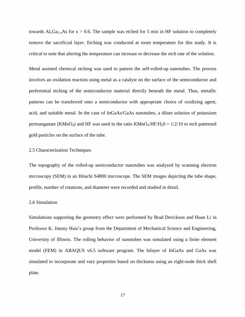
Figure 2.1 Schematic showing an example of a planar stack structure grown by metal organic chemical vapor
deposition (MOCVD) for fabrication of strain-induced semiconductor tubes. The stack contains an In0.3Ga0.7As
strained layer along with a GaAs quantum well (QW) layer grown between Al0.33Ga0.67As barrier layers on an
Al0.75Ga0.25As sacrificial layer.

20
Figure 2.2 Mask pattern designed in LASI software consisting of 19 × 50 µm rectangles oriented 45° to the wafer
cleaving edge <110> used for defining rectangular mesas on the planar structure.

21
CHAPTER III: EFFECT OF MESA GEOMETRY
3.1 Geometry Dependence Plot
For large area fabrication, it is important to ensure uniformity in diameter along the individual
tube and throughout the sample in every tube. It was reported that nanotubes rolled along the
<100> crystal orientation direction, irrespective of the stripe pattern orientation, because rolling
is influenced by the anisotropy of Young’s modulus in A3B
5 cubic crystals [13, 29, 49]. For
InxGa1-xAs-GaAs materials, the crystal is less stiff along <100> directions than along <110>
directions. Any variance from the <100> direction would result in a nanotube with a non-
uniform diameter. Thus, crystal direction was an important parameter in the formation of strain-
induced self-rolling nanotubes.
This thesis presents details on another parameter significant for the ordered large area assembly
of nanostructures. The self-rolling process of detached hetero-structures leading to micro- and
nano-objects has been demonstrated earlier for various geometries such as helices, spirals, tubes,
rings [22, 45, 50]. While a rectangular geometry is proposed for fabricating nanotubes, the effect
of stripe dimensions on the tube structure has not been studied.
Nanotubes required for the study were fabricated as described in Section 2.3 of Chapter II of this
thesis. Experiments were performed using stripe patterns with lengths and widths in the range of
5–100 µm on samples with diameters between 1–10 µm. The diameter can be precisely
predetermined in the epitaxial growth process in the range of a few hundreds of micrometers to
several nanometers. The experimental results were systematically studied and plotted on the
basis of tube circumference, rolling behavior, and mesa dimensions. Shown in Figure 3.1 are the

22
2-D and 3-D plots for the rolling behavior as a function of three parameters: the circumference c,
the length b, and the width a of the rectangular stripe pattern.
Based on the trends observed, the rolling behavior can be broadly classified into the following
two categories. One, when the circumference (c) of the tube is much larger than the width (c/a >
1) or the aspect ratio of the mesa rectangle is large (b/a >1), rolling always occurs from the long
side (b side). In the 2-D plot, this region is highlighted in yellow and extends along the far right
and top portion of the graph.
When the circumference is smaller than or equal to the width (c/a < 1), rolling can take place
from the long side, short side, or meta-stable, depending on the aspect ratio (b/a) of the mesa
pattern, as shown in the 2-D plot.
The meta-stable region in the 2-D plot is indicated for patterns that have a very low aspect ratio
or a tube circumference that is much smaller than the pattern width. In this region, rolling occurs
short side on one end and long side on the other end which produces a deadlock ‘meta-stable’
state where further rolling from either direction is restricted and tubes lose their tendency to roll.
The samples obtained in the meta-stable region contained either tubes with mixed transitions or a
blend of tubes rolled up at the short and long sides.
In the 3-D plot shown on the right in Figure 3.1, a clear demarcation in the rolling trends was
observed by introducing the width of the stripe pattern as the third axis. While long-side rolling
seems to be limited to shorter widths, mixed- and short-side rolling occurred for higher values
for the same aspect ratio. As the width of the strip pattern increases, a larger area is accessible to
the etchant and hence the possibility of short-side or even mixed rolling is fairly intuitive. For

23
shorter widths, the amount of area etched along the length is greater compared to the width; thus,
a larger area exposed to the etchant instigates long-side rolling.
From the plot, it can be derived that rolling largely depends on two factors, the width of the
stripe and the circumference of the tube. For tubes where c < a, the width of the pattern decides
the rolling behavior, whereas for c > a, rolling occurs generally long side. Very high aspect ratio
(b/a) patterns also are found to result in long-side rolled up tubes. A lot depends on the
circumference of the tube that is formed as a result of the strain between the bilayer structures.
The rolling direction is determined by the amount of strain in the bilayer and the energy released
when the bilayer is detached from the substrate. However, it is important to remember that the
strain in the bilayer solely governs the final diameter of the tube and, hence, is independent of
the stripe geometry or dimensions. Accordingly, rolling in either direction should and will not
change the diameter of the resultant tube.
3.2 General Trends: Long-Side, Short-Side and Mixed Rolling
With the rectangular stripes oriented along <100> (the soft direction), tubes with different
lengths and different numbers of rotations were formed. In the soft rolling direction, all four
sides of the rectangular mesa are crystallographically equivalent and, hence, have an equal
tendency to roll up during etching of the sacrificial layer. Depending on the length, width, and
the diameter of the bilayer (and concurrently the built-in strain and thickness), different trends
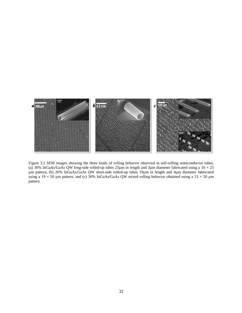
are observed. Figure 3.2, shows the three types of rolling trends obtained. Part (a) shows the
predominantly long-side rolled-up tubes fabricated with a 10 × 25 µm stripe pattern on an
In0.3Ga0.7As/GaAs stack. The diameter of these tubes is about 3µm. Shown in part (b) are the
short-side rolled-up tubes formed with a 19 × 50 µm rectangular stripe on an In0.2Ga0.8As/GaAs

24
stack with a diameter close to 4 µm. Part (c) displays a yield of long-side and short-side rolled-
up tubes fabricated using a 13 × 50 µm mesa pattern on an In0.3Ga0.7As/GaAs stack.
3.3 Time Evolution
In order to understand the mechanism involved in the rolling process, a time evolution of rolling
behavior was studied. Several samples of the same composition and mesa pattern were fabricated
and etched in dilute HF solution for different times, as described in the experimental section
earlier. The samples consisted of tubes fabricated using an In0.3Ga0.7As/GaAs stack with the 10 ×
25 µm strip to study long-side rolling behavior and an In0.2Ga0.8As/GaAs stack with 19 × 50 µm
strip pattern to study the rolling behavior occurring from short side. The dimensions of the
rectangular mesa were chosen so that the resultant tubes clearly pertained to the long-side and
short-side rolling regime. In the first example, 10 × 25 µm gave a b/a ratio of 2.5 and a c/a ratio
of 0.98. In the second example, 19 × 50 µm gave a b/a ratio of 2.63 and a c/a ratio of 0.66. These
two points are indicated on the 2-D plot (Figure 3.1) discussed earlier.
Shown in Figures 3.3 and 3.4 are the snapshots for both long-side and short-side rolled-up
behavior in nanotubes at the specified etching time. As discussed earlier, all four sides have an
equal tendency to roll up. Initially, after 30 s of etching, all four sides of the bilayer film tend to
curve as it starts to partially detach from the substrate during selective etching of the sacrificial
layer. This is shown in frame (a) in Figure 3.3 and Figure 3.4. The part of the sacrificial layer
that is still restricted to the substrate is the dark rectangular area visible in the centre of the strip.
In the case of long-side rolling (Figure 3.3), a stage (b) occurs where the bilayer film tends to
curve up from both the short side and the long side.
25
On further increasing the etching time to 55 s, a stage (c) occurs where long-side rolling
supersedes the short side. This provides a useful insight about the behavior of strained thin films
and the energy minimization process at the nanoscale level. The transition from stage (b) to stage
(c) can be explained on the basis of thermodynamic control. Since the length of the strip is longer
than the width, more area is etched along the length than the width at a particular time. This in
turn allows better access to the etchant and, thus, the tube assumes the length of the long side at
the end of 60 s, as shown in Figure 3.3 (d). It is presumed that the short side must have flattened
down in the process of energy minimization. In the case of short-side rolling (Figure 3.4), a
similar behavior is observed during initial etching of 30 s when all the four sides tend to curve up
(a). Interestingly enough, the etching times in this case are longer because of the larger pattern
(19 × 50 µm). Here, rolling from the short side predominates after 120 s of etching, as shown in
stage (b), and continues to form multi-turn tubes on each end until they are against each other as
the sacrificial layer is etched further for (c) 140 s and (d) 180 s, respectively. As the sacrificial
layer strip became narrower, a small tear in the tubular structure (i.e., a part of the bilayer film
was still attached to the substrate) was observed in almost all short-side rolled-up tubes.
3.4 Specific Ratio
In the size range studied, an interesting phenomenon occurred in samples with the specific ratio
of 2.63 (b/a = 2.63). All the tubes formed with this specific ratio rolled up from the short side. A
comparison between samples of three different diameters fabricated with the same mesa
dimensions was done. Shown in Figure 3.5 (a, b, and c), are short-side rolled-up tubes fabricated
using a 19 × 50 µm pattern on samples with diameters of 4, 7, and 9 µm. For an even
comparison, the diameters were varied only by altering the thickness of the barrier layer in the
stack and not the built-in strain. All samples consisted of an In0.2Ga0.8As/GaAs bilayer. Figure

26
3.5 (d, e, and f) shows short-side rolled-up tubes formed using patterns 19 × 50, 29 × 75, 38 ×
100 µm on three samples with a diameter of 4 µm. Thus, regardless of the absolute a and b
dimensions, and diameter, at this ratio, the patterned membranes resulted in short-side rolled-up
nanotubes. The specific aspect ratio for the short side observed in Figure 3.5 does not have a
significant physical meaning, other than the fact that it seems to lead to an intermediate state that
favors short-side rolling. Although a definite hypothesis of this phenomenon could not be
proposed, the observation could be useful for practical applications.
However, it is important to remember that the strain in the bilayer solely governs the final
diameter of the tube and, hence, is independent of the stripe geometry or dimensions.
Accordingly, rolling in either direction should and will not change the diameter of the resultant
tube.
3.5 Comparison with Simulated Results
To support these experimental results, collaboration with Professor Hsia’s group was initiated to
simulate the rolling behavior of nanotubes. Based on the finite element model created, a
comparison between the energy states associated with the two rolling directions was performed.
Figure 3.6 shows the energy states associated with three kinds of rolling behavior. It is calculated
that rolling along the long side has the lowest energy state and is preferable, because built-in
strain in the bilayer is most relaxed in this case. Note that for the simulations, the driving force
for rolling is analogous to the release of the bilayer with time. Promisingly, the enlarged view in
Figure 3.6 (b) shows energy states during initial time and indeed is consistent with the
experimental results in that mixed rolling is the lowest energy state. This is in good agreement
with our experimental results in the time evolution study, where both long and short side rolling

27
begin with all four sides curving up (Figure 3.3). Figure 3.7 shows the rolling behavior for two
mesa patterns (a) using the 19 × 50 µm pattern and (b) using the 4 × 25 µm pattern etched to
40% of the total area. While it is true that rolling begins to occur from both sides for either
geometry, the extent of etching differs along the length and width of the mesa, which ultimately
decides the rolling direction. The simulation and experimental results shown here imply that the
rolling history could very well drive the rolling along a different direction depending on the
intermediate state of the deformation. In Figure 3.7 (a), it is seen that the extent of etching along
the width of the mesa is greater than along the length. The edge along with the width is lifted
completely, whereas a part of the length and corner still remain pinned, which naturally leads to
short side rolling behavior.
By contrast, Figure 3.7 (b) shows an almost opposite rolling behavior in that the corner and
length are etched more than the width of the mesa, which leads to a long-side rolled-up tube.
These simulations again support experimental data that indicate short-side rolling for 19 × 50 µm
and long-side rolling for 4 × 25 µm strip dimensions as plotted in earlier Figure 3.1.
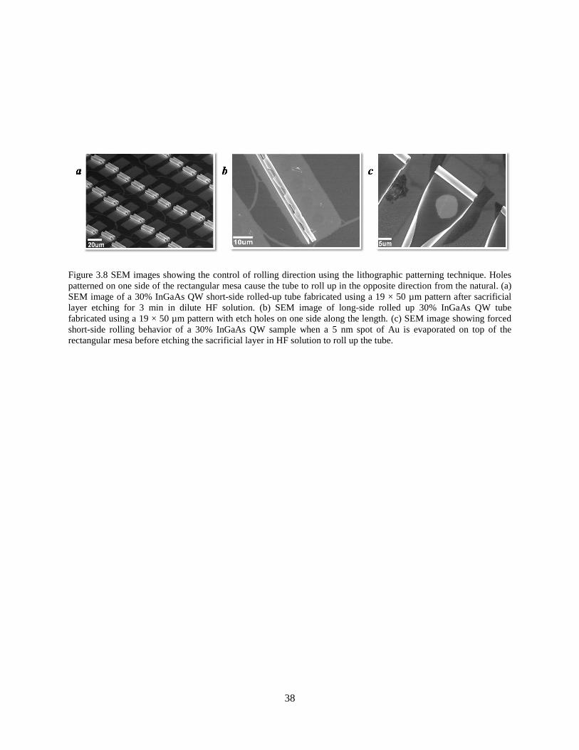
3.6 Forced Rolling
This study is noteworthy because it can be used to predict the rolling behavior in the design
stages prior to on-site fabrication. While this is true, at certain times it is necessary to defeat the
naturally occurring thermodynamic energy release process to achieve specific shape, length, and
tube orientation. In this case, the nanotube structure can be engineered to roll up short or long
side by introducing etch holes on the mesa pattern to induce a fraction of anisotropy. By
introducing etch holes, the concept of kinetics comes into play. During etching, the areas
surrounding the holes are etched faster and provide better passage to the etchant, thereby creating

28
an asymmetry in etching between the penetrable (with holes) and sealed areas (without holes).
Shown in Figure 3.8 (a) is one such example where the rectangular mesa dimensions yield a
short-side rolled-up tube. By introducing an array of uniform holes on one side of the rectangular
stripe, the tube rolls up along the length as shown in Figure 3.8 (b). Note that the patterning of
the rolled-up bilayer does not affect the diameter. It would be counter- intuitive that the
introduction of holes had little or no effect on the internal strain in the bilayer or cause atypical,
non-uniform rolling. However, this can be explained on the basis of discrete and uniform strain
distribution. It is for the same reason that the introduction of quantum wells or quantum dots
uniformly in the microtube wall does not cause uneven rolling or strain. The idea is to introduce
an asymmetry in etching, which causes rolling to dominate in one direction. While holes were
used to demonstrate this idea, other uniform geometries such as squares, rectangles, and ellipses
can also be implemented. Conversely, a restrain can be used on the rectangular mesa that
restricts etching in that direction. As a result, the etchant tries to circumvent the restrain and
etches the bilayer mesa from an accessible region. Figure 3.8 (c) shows, for instance, how a
circular area on the rectangular mesa evaporated with a thin layer (5 nm) of metallic gold, holds
down the film in that direction. The tube rolls up from the opposite end, as shown in the figure.
3.7 Patterning Tubes using Metal-Assisted Chemical Etching
Metal-assisted chemical etching [51-53] is a contemporary top-down and scalable approach for
fabricating three-dimensional nanostructures. Using this method, nanotubes can be patterned to
form functional structures that can be used in plasmonic enhancement, photonic device crystals,
DBR (distributed bragg reflectors) lasers. It has been demonstrated earlier [16, 34, 36] that
geometry can play an active role in varying the optical properties of the nanotube.
29
Modifying the edge geometry to create a bottle-like triangular notch or to etch periodic structures
such as DBR gratings on the mesa enhances the optical confinement in nanotubes. Moreover,
nanotubes with a periodic array of holes can be designed to be used in 3-D photonic crystals.
Although this can be done using traditional lithographic techniques as described in the previous
section, the resolution and scalability becomes a limiting factor. With metal-assisted chemical
etching, tubes can be patterned in the nanoscale range. During metal-assisted chemical etching,
the metal on the semiconductor surface acts as a local cathode and a catalyst to promote the
oxidation reaction [54, 55]. The etch rate depends directly on the rate at which the oxidant
(KMnO4) can generate holes under the metal particle and indirectly the concentration of the
solution. Shown in Figure 3.9 (a), is an SEM image of a 30% InGaAs QW semi-porous long-side
rolled-up tube fabricated using metal-assisted etching. Gold (Au) nanoparticle islands obtained
by evaporation of 1.5 nm of Au on the rolled-up tube are etched in a solution of HF:KMnO4:DI
(2:1:10) for 10 s. The detailed fabrication procedure has been described in Section 2.3 of this
thesis. Figure 3.9 (b) presents a magnified view of the surface of the nanotube. It is seen that the
etching only occurred in dense areas where metal nanoparticles were found in clusters. A non-
uniform deposition of Au on the surface of the nanotube could be the possible reason for site-
selective etching. Subsequently, evaporation was performed before rolling up the tube structure
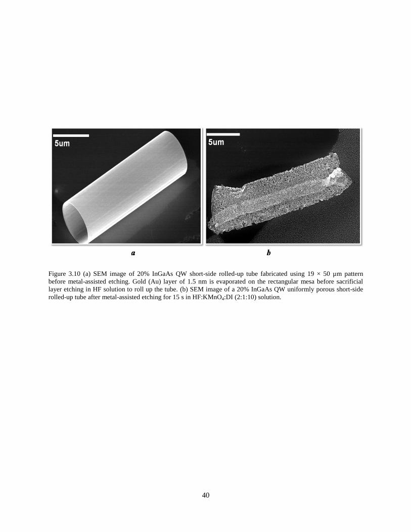
to ensure a uniform distribution on the surface of the rectangular mesa. Shown in Figure 3.10 (b)
is an SEM image of a 20% InGaAs QW uniform and porous short-side rolled-up tube after
metal-assisted chemical etching for 15 s in HF:KMnO4:DI (2:1:10) solution. In comparison with
Figure 3.10 (a), the tube appears to be collapsed due to the porosity.
The potential of metal-assisted chemical etching to create nanostructures extends far from the
preliminary results demonstrated in this work. The versatility in the process allows the formation

30
of various patterned nanostructures merely by controlling the etching concentration, etching
time, and type of metal used. Such a process could be used to pattern nanotubes with ordered
periodic arrays of holes to design photonic crystal cavity structures, which could be future
extensions of this project.

31
3.8 Figures
Figure 3.1 (a) 2-dimensional and (b) 3-dimensional plots summarizing rolling behavior as a function of
circumference of the tube (c), width (a), and length (b) of the rectangular strip pattern. Each unique rolling behavior
is color coded (blue: long side, red: short side, green: mixed) on the plot. Patterns with very high aspect ratios (far
right) always roll long side as shown in the yellow highlighted region of the 2-D plot. Rolling depends on the tube
diameter for smaller aspect ratios, as indicated in the bottom left of the 2-D plot. For the same aspect ratio (3-D
plot), long side rolling seems to be limited to shorter widths, and mixed and short side rolling are more likely to
occur for bigger stripes.
32
Figure 3.2 SEM images showing the three kinds of rolling behavior observed in self-rolling semiconductor tubes.
(a) 30% InGaAs/GaAs QW long-side rolled-up tubes 25µm in length and 3µm diameter fabricated using a 10 × 25
µm pattern, (b) 20% InGaAs/GaAs QW short-side rolled-up tubes 19µm in length and 4µm diameter fabricated
using a 19 × 50 µm pattern, and (c) 30% InGaAs/GaAs QW mixed rolling behavior obtained using a 13 × 50 µm
pattern.

33
Figure 3.3 SEM images of 30% InGaAs/GaAs QW long-side rolled-up tubes 25µm in length and 3µm diameter
fabricated using a 10 × 25 µm mesa pattern, formed after sacrificial Al0.75Ga0.25As layer etching for (a) 30 s, (b) 45 s,
(c) 55 s and (d) 60 s in 1:2 HF:DI solution. As the bilayer is released from the substrate, the bilayer lifts up in both
directions. Increasing etch times shows preferential long-side rolling.

34
Figure 3.4 SEM images of 20% InGaAs/GaAs QW short-side rolled-up tubes 19µm in length and 4µm diameter
fabricated using a 19 × 50 µm mesa pattern, formed after sacrificial Al0.75Ga0.25As layer etching for (a) 30 s, (b) 120
s, (c) 140 s and (d) 180 s in 1:2 HF:DI solution. As the bilayer is released from the substrate, the bilayer lifts up in
both directions. Increasing etch times shows preferential short-side rolling. Note that a tear developed during the
rolling process.

35
Figure 3.5 SEM images of short-side rolled-up tubes obtained using a 19 × 50 µm pattern on 20% InGaAs/GaAs
QW samples with diameter (a) 4 µm, (b) 7 µm and (c) 9 µm after sacrificial layer etching for 3 mins in 1:2 HF:DI
solution. SEM images of short-side rolled-up tubes using (d) 19 × 50 µm, (e) 28 × 75 µm and (f) 38 × 100 µm
patterns on samples with diameter of 4 µm.

36
a
b
Figure 3.6 (a) Graph showing the simulation results of the energy state of a strained membrane, where the x-axis is
the driving force for rolling and the y axis is the total energy of the geometry. Long-side rolling is the lowest energy
state at equilibrium condition. (b) Enlargement of area shown in (a), showing the relationship between strain energy
and rolling force during initial etching time. Mixed rolling is the lowest energy state initially.
0
0.005
0.01
0.015
0.02
0.025
0 0.001 0.002 0.003 0.004 0.005
Str
ain
En
erg
y (
arb
itra
ry u
nit
)
Rolling Force (arbitrary unit)
Mixed
Short
Long
0.00E+00
5.00E-07
1.00E-06
1.50E-06
2.00E-06
2.50E-06
0.0E+00 5.0E-07 1.0E-06 1.5E-06 2.0E-06 2.5E-06 3.0E-06
Str
ain
En
ergy (
arbit
rary
unit
)
Rolling Force (arbitrary unit)
Mixed
Short
Long

37
Figure 3.7 Simulation results showing a comparison between etching behavior of two different patterns. (a) 19 × 50
µm pattern, showing the corner and a small area along the length are pinned compared to the width. (b) 4 × 25 µm
pattern, showing the corner is lifted and most of the length is etched compared to the width. These behaviors reflect
opposing rolling directions and are experimentally verified for short- and long-side rolling, respectively.
38
Figure 3.8 SEM images showing the control of rolling direction using the lithographic patterning technique. Holes
patterned on one side of the rectangular mesa cause the tube to roll up in the opposite direction from the natural. (a)
SEM image of a 30% InGaAs QW short-side rolled-up tube fabricated using a 19 × 50 µm pattern after sacrificial
layer etching for 3 min in dilute HF solution. (b) SEM image of long-side rolled up 30% InGaAs QW tube
fabricated using a 19 × 50 µm pattern with etch holes on one side along the length. (c) SEM image showing forced
short-side rolling behavior of a 30% InGaAs QW sample when a 5 nm spot of Au is evaporated on top of the
rectangular mesa before etching the sacrificial layer in HF solution to roll up the tube.

39
Figure 3.9 (a) SEM images of 30% InGaAs QW semi-porous long-side rolled-up tube fabricated using metal-
assisted etching. Gold (Au) nanoparticle islands obtained by evaporation of 1.5 nm of Au on the rolled-up tube are
etched in a solution of HF:KMnO4:DI (2:1:10) for 15 s. (b) Magnified view of (a) showing porosity in regions where
Au nanoparticles are dense.
40
Figure 3.10 (a) SEM image of 20% InGaAs QW short-side rolled-up tube fabricated using 19 × 50 µm pattern
before metal-assisted etching. Gold (Au) layer of 1.5 nm is evaporated on the rectangular mesa before sacrificial
layer etching in HF solution to roll up the tube. (b) SEM image of a 20% InGaAs QW uniformly porous short-side
rolled-up tube after metal-assisted etching for 15 s in HF:KMnO4:DI (2:1:10) solution.
41
CHAPTER IV: CONCLUSION
4.1 Summary
In conclusion, yet another parameter significant for ordered large area assembly of self-rolled-up
semiconductor tubes, i.e., the effect of the geometry of bilayer mesa on the tube shape, has been
discussed in detail. The rolling direction is a result of an energy minimization process that the
planar film undergoes at equilibrium condition when it is detached from the substrate. The
dimension of the stripe pattern plays an important role because it determines the extent of
anisotropic etching of the bilayer. Depending on the extent of anisotropy in etching, the energy
associated with the release differs along the length and width of the rectangular strip; thus, a
different rolling behavior is observed.
The rolling behavior can be broadly classified into two categories: tubes that roll up along the
length of the mesa and short-side rolled-up tubes. Usually, patterns with a high aspect ratio tend
to roll up long side, while patterns with comparable widths and lengths exhibit a different rolling
behavior, depending on the circumference of the tube. Simulation results of strained bilayers for
various geometries demonstrated that rolling along the long side is the lowest energy state,
probably because the built-in strain in the bilayer is most relaxed in this state. The simulated and
experimental results consistently establish the fact that rolling begins from all four sides of the
mesa despite the geometry and later takes over either direction, depending on the anisotropy in
etching. By means of this analysis, the factors affecting the rolling behavior can be carefully
controlled to ensure uniformity in tubes for large area fabrication.
This thesis also provides insights on engineering tube geometry through forced rolling or
patterning. The characteristic rolling behavior of semiconductor tubes can be remodeled by

42
introducing etch holes or through metal-assisted chemical etching. Indeed, it is critical to be able
to conceive and control the rolling direction in order to design tubes for a specific length and
number of rotations.
4.2 Potential Application and Future Directions
Nanotechnology has the potential to create many new structures and devices with a vast range
of applications in medicine, electronics, and energy production. An emerging class of 3-D
nanostructures and objects can be fabricated by strain-driven engineering: a combinatorial
approach that uses top-down and bottom-up fabrication methods to form self-rolling structures.
One such example is semiconductor tubes, which can be embedded with versatile hetero-
junctions and active materials in the tube wall that make them unique in the world of
nanostructures. By providing an additional third dimension, the out-of-plane curvature, the
functionality of microtube optics extends beyond the conventional planar structures.
This additional dimension helps to control the internal strain in the system, thereby intrinsically
modifying the optical properties of the microtube. Much can be done in this area by designing
the tube geometry to produce low-threshold optical devices such as resonators or lasers. By
including a metal layer in the tube wall, the concept of plasmonics can be introduced to design a
wide range of possible plasmonic-based devices and low detection limit sensing applications.
Biological materials such as DNA or chromosomes can be embedded inside the tube wall and
can be used as drug delivery vehicles or for cancer detection. By patterning semiconductor tubes
with a periodic array of holes, the possibility they can be used as photonic crystals can be
explored.

43
REFERENCES
[1] D. Vasileska, H. R. Khan, S. S. Ahmed, C. Ringhofer, and C. Heitzinger, "Quantum and
Coulomb effects in nanodevices," International Journal of Nanoscience, vol. 4, pp. 305-
361, 2005.
[2] J. D. Meindl and M. Tobman, "The coming era of microelectronics," in 16th Annual
Symposium on Frequency Control, 1962, pp. 211-226, 1962.
[3] I. Vurgaftman, J. R. Meyer, and L. R. Ram-Mohan, "Band parameters for III-V
compound semiconductors and their alloys," Journal of Applied Physics, vol. 89, pp.
5815-5875, Jun. 2001.
[4] J. Kwo and M. Hong, "Research advances on III-V MOSFET electronics beyond Si
CMOS," Journal of Crystal Growth, vol. 311, pp. 1944-1949, Mar. 2009.
[5] B. Kelley, B. Dodrill, J. Lindemuth, G. Du, and J. R. Meyer, "Electronic transport
characterization of HEMT structures," Solid State Technology, vol. 43, pp. 130-135, Dec
2000.
[6] B. Bo, X. Tang, B. Zhang, G. Huang, Y. Zhang, and T. S. Chuan, "Lasing properties of
AlGaAs/GaAs material diode lasers grown by MOCVD using TBA in N2 ambient,"
Journal of Crystal Growth, vol. 268, pp. 415-419, 2004.
[7] S.-j. Hon, C. T. Kuo, T. P. Chen, and M. H. Hsieh, "High-power GaN LED chip with low
thermal resistance," in Gallium Nitride Materials and Devices III, San Jose, CA, USA, p.
689411, 2008.
[8] I. L. Fang, H. w. Huang, C. Ching-Hua, C. F. Lai, T. C. Lu, H. C. Kuo, and S. C. Wang,
"InGaN/GaN MQW nanorods LED fabricated by ICP-RIE and PEC oxidation
processes," in Conference on Lasers and Electro-Optics/Quantum Electronics and Laser
Science Conference and Photonic Applications Systems Technologies, p. CMO3, 2007.
[9] R. Dahal, B. Pantha, J. Li, J. Y. Lin, and H. X. Jiang, "InGaN/GaN multiple quantum
well solar cells with long operating wavelengths," Applied Physics Letters, vol. 94, p.
063505, 2009.
[10] S. A. Fortuna, J. G. Wen, I. S. Chun, and X. L. Li, "Planar GaAs nanowires on GaAs
(100) substrates: self-aligned, nearly twin-defect free, and transfer-printable," Nano
Letters, vol. 8, pp. 4421-4427, Dec. 2008.
[11] C. Ik Su and L. Xiuling, "Controlled assembly and dispersion of strain-induced
InGaAs/GaAs nanotubes," IEEE Transactions on Nanotechnology, vol. 7, pp. 493-495,
2008.

44
[12] V. Y. Prinz, A. V. Chekhovskiy, V. V. Preobrazhenskii, B. R. Semyagin, and A. K.
Gutakovsky, "A technique for fabricating InGaAs/GaAs nanotubes of precisely
controlled lengths," Nanotechnology, vol. 13, pp. 231-233, 2002.
[13] V. Y. Prinz, V. A. Seleznev, A. K. Gutakovsky, A. V. Chehovskiy, V. V.
Preobrazhenskii, M. A. Putyato, and T. A. Gavrilova, "Free-standing and overgrown
InGaAs/GaAs nanotubes, nanohelices and their arrays," Physica E: Low-Dimensional
Systems and Nanostructures, vol. 6, pp. 828-831, 2000.
[14] R. H. Baughman, A. A. Zakhidov, and W. A. de Heer, "Carbon nanotubes--The route
toward applications," Science, vol. 297, pp. 787-792, 2002.
[15] M. Zheng, A. Jagota, E. D. Semke, B. A. Diner, R. S. McLean, S. R. Lustig, R. E.
Richardson, and N. G. Tassi, "DNA-assisted dispersion and separation of carbon
nanotubes," Nature Materials, vol. 2, pp. 338-342, 2003.
[16] F. Li, Z. Mi, and S. Vicknesh, "Coherent emission from ultrathin-walled spiral
InGaAs/GaAs quantum dot microtubes," Optics Letters, vol. 34, pp. 2915-2917, 2009.
[17] S. Iijima, "Helical microtubules of graphitic carbon," Nature, vol. 354, pp. 56-58, 1991.
[18] D. Gong, C. A. Grimes, O. K. Varghese, W. C. Hu, R. S. Singh, Z. Chen, and E. C.
Dickey, "Titanium oxide nanotube arrays prepared by anodic oxidation," Journal of
Materials Research, vol. 16, pp. 3331-3334, Dec. 2001.
[19] X. C. Jiang, B. Mayers, T. Herricks, and Y. N. Xia, "Direct synthesis of Se@CdSe
nanocables and CdSe nanotubes by reacting cadmium salts with Se nanowires,"
Advanced Materials, vol. 15, pp. 1740-1743, Oct. 2003.
[20] Y. J. Xing, Z. H. Xi, X. D. Zhang, J. H. Song, R. M. Wang, J. Xu, Z. Q. Xue, and D. P.
Yu, "Nanotubular structures of zinc oxide," Solid State Communications, vol. 129, pp.
671-675, Mar. 2004.
[21] S. V. Golod, V. Y. Prinz, V. I. Mashanov, and A. K. Gutakovsky, "Fabrication of
conducting GeSi/Si micro- and nanotubes and helical microcoils," Semiconductor
Science and Technology, vol. 16, pp. 181-185, 2001.
[22] V. Y. Prinz, "Precise, molecularly thin semiconductor shells: From nanotubes to
nanocorrugated quantum systems," Physica Status Solidi (B), vol. 243, pp. 3333-3339,
2006.
[23] E. P. A. M. Bakkers and M. A. Verheijen, "Synthesis of InP nanotubes," Journal of the
American Chemical Society, vol. 125, pp. 3440-3441, 2003.

45
[24] F. Scholz, S. B. Thapa, M. Fikry, J. Hertkorn, T. Wunderer, F. Lipski, A. Reiser, Y. Xie,
M. Feneberg, K. Thonke, R. Sauer, M. Durrschnabel, L. D. Yao, and D. Gerthsen,
"Epitaxial growth of coaxial GaInN-GaN hetero-nanotubes," IOP Conference Series:
Materials Science and Engineering, vol. 6, issue 1, p. 012002, 2009.
[25] W. Qiang, H. Zheng, L. Chun, W. Xizhang, C. Yi, and L. Yinong, "Synthesis and optical
properties of gallium phosphide nanotubes," ChemInform, vol. 37, p. 03217, 2006.
[26] X. Li, "Strain induced semiconductor nanotubes: From formation process to device
applications," Journal of Physics D: Applied Physics, vol. 41, p. 193001, 2008.
[27] A. B. Vorob'ev and V. Y. Prinz, "Directional rolling of strained heterofilms,"
Semiconductor Science and Technology, vol. 17, pp. 614-616, 2002.
[28] W. A. Brantley, "Calculated elastic constants for stress problems associated with
semiconductor devices," Journal of Applied Physics, vol. 44, pp. 534-535, 1973.
[29] R. I. Cottam and G. A. Saunders, "The elastic constants of GaAs from 2 K to 320 K,"
Journal of Physics C: Solid State Physics, vol. 6, pp. 2105-2118, 1973.
[30] T. Kipp, "Optical microtube ring cavities," in Advances in Solid State Physics, 2008, pp.
17-28.
[31] T. Kipp, H. Welsch, C. Strelow, C. Heyn, and D. Heitmann, "Optical modes in
semiconductor microtube ring resonators," Physical Review Letters, vol. 96, pp. 077403
(1-4), 2006.
[32] F. Li and Z. Mi, "Optically pumped rolled-up InGaAs/GaAs quantum dot microtube
lasers," Optics Express, vol. 17, pp. 19933-19939, 2009.
[33] K. Kubota, P. O. Vaccaro, N. Ohtani, Y. Hirose, M. Hosoda, and T. Aida,
"Photoluminescence of GaAs/AlGaAs micro-tubes containing uniaxially strained
quantum wells," Physica E: Low-Dimensional Systems and Nanostructures, vol. 13, pp.
313-316, 2002.
[34] C. Strelow, H. Rehberg, C. M. Schultz, H. Welsch, C. Heyn, D. Heitmann, and T. Kipp,
"Optical microcavities formed by semiconductor microtubes using a bottlelike
geometry," Physical Review Letters, vol. 101, pp. 127403-4, 2008.
[35] Z. Mi, S. Vicknesh, F. Li, and P. Bhattacharya, "Self-assembled InGaAs/GaAs quantum
dot microtube coherent light sources on GaAs and silicon," in Silicon Photonics IV, San
Jose, CA, USA, pp. 72200S-72200S-9, 2009.
[36] C. Strelow, H. Rehberg, C. M. Schultz, H. Welsch, C. Heyn, D. Heitmann, and T. Kipp,
"Spatial emission characteristics of a semiconductor microtube ring resonator," Physica
E: Low-Dimensional Systems and Nanostructures, vol. 40, pp. 1836-1839, 2008.

46
[37] C. Strelow, M. Sauer, S. Fehringer, T. Korn, C. Schüller, A. Stemmann, C. Heyn, D.
Heitmann, and T. Kipp, "Time-resolved studies of a rolled-up semiconductor microtube
laser," Applied Physics Letters, vol. 95, pp. 221115 (1-3), 2009.
[38] S. Vicknesh, F. Li, and Z. Mi, "Optical microcavities on Si formed by self-assembled
InGaAs/GaAs quantum dot microtubes," Applied Physics Letters, vol. 94, p. 081101,
2009.
[39] A. V. Prinz and V. Y. Prinz, "Application of semiconductor micro- and nanotubes in
biology," Surface Science, vol. 532-535, pp. 911-915, 2003.
[40] A. V. Prinz, V. Y. Prinz, and V. A. Seleznev, "Semiconductor micro- and nanoneedles
for microinjections and ink-jet printing," Microelectronic Engineering, vol. 67-68, pp.
782-788, 2003.
[41] G. S. Huang, Y. F. Mei, D. J. Thurmer, E. Coric, and O. G. Schmidt, "Rolled-up
transparent microtubes as two-dimensionally confined culture scaffolds of individual
yeast cells," Lab on a Chip, vol. 9, pp. 263-268, 2009.
[42] C. Giordano, M. T. Todaro, A. Salhi, L. Martiradonna, I. Viola, A. Passabì, L. Carbone,
G. Gigli, A. Passaseo, and M. De Vittorio, "Nanocrystals cylindrical microcavities
exploiting thin-walled InGaAs/GaAs microtubes," Microelectronic Engineering, vol. 84,
pp. 1408-1411, 2007.
[43] N. Shaji, H. Qin, I. Knezevic, C. Deneke, O. G. Schmidt, M. A. Eriksson, and R. H.
Blick, "Electron transport in curved low dimensional electron systems," in
Nonequilibrium Carrier Dynamics in Semiconductors, pp. 1-5, 2006.
[44] A. B. Vorob'ev, V. Y. Prinz, Y. S. Yukecheva, and A. I. Toropov, "Magnetotransport
properties of two-dimensional electron gas on cylindrical surface," Physica E: Low-
Dimensional Systems and Nanostructures, vol. 23, pp. 171-176, 2004.
[45] V. Y. Prinz, V. A. Seleznev, A. V. Prinz, and A. V. Kopylov, "3D heterostructures and
systems for novel MEMS/NEMS," Science and Technology of Advanced Materials, vol.
10, p. 034502, 2009.
[46] I. S. Chun, V. B. Verma, V. C. Elarde, S. W. Kim, J. M. Zuo, J. J. Coleman, and X. Li,
"InGaAs/GaAs 3D architecture formation by strain-induced self-rolling with
lithographically defined rectangular stripe arrays," Journal of Crystal Growth, vol. 310,
pp. 2353-2358, 2008.
[47] I. Barycka and I. Zubel, "Chemical etching of (100) GaAs in a sulphuric acid-hydrogen
peroxide-water system," Journal of Materials Science, vol. 22, pp. 1299-1304, 1987.

47
[48] H. G. Lee, M. S. Jusoh, A. Dolah, A. Yusof, M. R. Yahya, and B. Y. Majlis, "The study
of etching selectivity between InGaAs and AlGaAs in acid based etching solution," in
Proceedings ICSE 2004 - 2004 IEEE International Conference on Semiconductor
Electronics, pp. 423-426, 2004.
[49] S. Mendach, O. Schumacher, C. Heyn, S. Schnüll, H. Welsch, and W. Hansen,
"Preparation of curved two-dimensional electron systems in InGaAs/GaAs-microtubes,"
Physica E: Low-Dimensional Systems and Nanostructures, vol. 23, pp. 274-279, 2004.
[50] V. Y. Prinz, D. Grutzmacher, A. Beyer, C. David, B. Ketterer, and E. Deckardt, "A new
technique for fabricating three-dimensional micro- and nanostructures of various shapes,"
Nanotechnology, vol. 12, pp. 399-402, 2001.
[51] I. S. Chun, E. K. Chow, and X. Li, "Nanoscale three dimensional pattern formation in
light emitting porous silicon," Applied Physics Letters, vol. 92, p. 191113, 2008.
[52] Y. Yasukawa, H. Asoh, and S. Ono, "Site-selective chemical etching of GaAs through a
combination of self-organized spheres and silver particles as etching catalyst,"
Electrochemistry Communications, vol. 10, pp. 757-760, 2008.
[53] Y. Yasukawa, H. Asoh, and S. Ono, "Site-selective metal patterning/metal-assisted
chemical etching on GaAs substrate through colloidal crystal templating," Journal of The
Electrochemical Society, vol. 156, pp. H777-H781, 2009.
[54] X. Li and P. W. Bohn, "Metal-assisted chemical etching in HF/H2O2 produces porous
silicon," Applied Physics Letters, vol. 77, pp. 2572-2574, 2000.
[55] T. Hadjersi, N. Gabouze, E. S. Kooij, A. Zinine, A. Ababou, W. Chergui, H. Cheraga, S.
Belhousse, and A. Djeghri, "Metal-assisted chemical etching in HF/Na2S2O8 or
HF/KMnO4 produces porous silicon," Thin Solid Films, vol. 459, pp. 271-275, 2004.