Embed Size (px)
Citation preview

Introduction toCMOS VLSI
Design
SPICE Simulation

Slide 2CMOS VLSI Design
Outline Introduction to SPICE DC Analysis Transient Analysis Subcircuits Optimization Power Measurement Logical Effort Characterization

Slide 3CMOS VLSI Design
Introduction to SPICE Simulation Program with Integrated Circuit Emphasis
– Developed in 1970’s at Berkeley– Many commercial versions are available– HSPICE is a robust industry standard
• Has many enhancements that we will use Written in FORTRAN for punch-card machines
– Circuits elements are called cards– Complete description is called a SPICE deck

Slide 4CMOS VLSI Design
Writing Spice Decks Writing a SPICE deck is like writing a good program
– Plan: sketch schematic on paper or in editor• Modify existing decks whenever possible
– Code: strive for clarity• Generously comment
– Test:• Predict what results should be• Compare with actual• Garbage In, Garbage Out!

Slide 5CMOS VLSI Design
Example: RC Circuit* rc.sp* [email protected] 2/2/03* Find the response of RC circuit to rising input
*------------------------------------------------* Parameters and models*------------------------------------------------.option post
*------------------------------------------------* Simulation netlist*------------------------------------------------Vin in gnd pwl 0ps 0 100ps 0 150ps 1.8 800ps 1.8R1 in out 2kC1 out gnd 100f
*------------------------------------------------* Stimulus*------------------------------------------------.tran 20ps 800ps.plot v(in) v(out).end
R1 = 2K
C1 =100fF
Vin
+Vout
-

Slide 6CMOS VLSI Design
Result (Textual)legend: a: v(in) b: v(out) time v(in) (ab ) 0. 500.0000m 1.0000 1.5000 2.0000 + + + + + 0. 0. -2------+------+------+------+------+------+------+------+- 20.0000p 0. 2 + + + + + + + + 40.0000p 0. 2 + + + + + + + + 60.0000p 0. 2 + + + + + + + + 80.0000p 0. 2 + + + + + + + + 100.0000p 0. 2 + + + + + + + + 120.0000p 720.000m +b + + a+ + + + + + 140.0000p 1.440 + b + + + + + a + + + 160.0000p 1.800 + +b + + + + + +a + 180.0000p 1.800 + + b + + + + + +a + 200.0000p 1.800 -+------+------+b-----+------+------+------+------+a-----+- 220.0000p 1.800 + + + b + + + + +a + 240.0000p 1.800 + + + +b + + + +a + 260.0000p 1.800 + + + + b + + + +a + 280.0000p 1.800 + + + + b+ + + +a + 300.0000p 1.800 + + + + +b + + +a + 320.0000p 1.800 + + + + + b + + +a + 340.0000p 1.800 + + + + + b + + +a + 360.0000p 1.800 + + + + + b + +a + 380.0000p 1.800 + + + + + +b + +a + 400.0000p 1.800 -+------+------+------+------+------+--b---+------+a-----+- 420.0000p 1.800 + + + + + + b + +a + 440.0000p 1.800 + + + + + + b + +a + 460.0000p 1.800 + + + + + + b+ +a + 480.0000p 1.800 + + + + + + b +a + 500.0000p 1.800 + + + + + + +b +a + 520.0000p 1.800 + + + + + + +b +a + 540.0000p 1.800 + + + + + + + b +a + 560.0000p 1.800 + + + + + + + b +a + 580.0000p 1.800 + + + + + + + b +a + 600.0000p 1.800 -+------+------+------+------+------+------+---b--+a-----+- 620.0000p 1.800 + + + + + + + b +a + 640.0000p 1.800 + + + + + + + b +a + 660.0000p 1.800 + + + + + + + b +a + 680.0000p 1.800 + + + + + + + b +a + 700.0000p 1.800 + + + + + + + b+a + 720.0000p 1.800 + + + + + + + b+a + 740.0000p 1.800 + + + + + + + b+a + 760.0000p 1.800 + + + + + + + b+a + 780.0000p 1.800 + + + + + + + ba + 800.0000p 1.800 -+------+------+------+------+------+------+------ba-----+- + + + + +

Slide 7CMOS VLSI Design
Result (Graphical)
t(s)0.0 100p 200p 300p 400p 500p 600p 700p 800p 900p
0.0
0.5
1.0
1.5
2.0 v(in)
v(out)

Slide 8CMOS VLSI Design
Sources DC Source
Vdd vdd gnd 2.5
Piecewise Linear SourceVin in gnd pwl 0ps 0 100ps 0 150ps 1.8 800ps 1.8
Pulsed SourceVck clk gnd PULSE 0 1.8 0ps 100ps 100ps 300ps 800ps
PULSE v1 v2 td tr tf pw per
v1
v2
td tr tfpw
per

Slide 9CMOS VLSI Design
SPICE ElementsLetter ElementR ResistorC CapacitorL InductorK Mutual InductorV Independent voltage sourceI Independent current sourceM MOSFETD DiodeQ Bipolar transistorW Lossy transmission lineX SubcircuitE Voltage-controlled voltage sourceG Voltage-controlled current sourceH Current-controlled voltage sourceF Current-controlled current source

Slide 10CMOS VLSI Design
UnitsLetter Unit Magnitude
a atto 10-18
f fempto 10-15
p pico 10-12
n nano 10-9
u micro 10-6
m mili 10-3
k kilo 103
x mega 106
g giga 109
Ex: 100 femptofarad capacitor = 100fF, 100f, 100e-15
Slide 11CMOS VLSI Design
DC Analysis* mosiv.sp
*------------------------------------------------* Parameters and models*------------------------------------------------.include '../models/tsmc180/models.sp'.temp 70.option post
*------------------------------------------------ * Simulation netlist*------------------------------------------------*nmosVgs g gnd 0Vds d gnd 0M1 d g gnd gnd NMOS W=0.36u L=0.18u
*------------------------------------------------* Stimulus*------------------------------------------------.dc Vds 0 1.8 0.05 SWEEP Vgs 0 1.8 0.3.end
Vgs Vds
Ids
4/2

Slide 12CMOS VLSI Design
I-V Characteristics
Vds
0.0 0.3 0.6 0.9 1.2 1.5 1.8
Ids(A)
0
50
100
150
200
250
Vgs = 1.8
Vgs = 1.5
Vgs = 1.2
Vgs = 0.9
Vgs = 0.6
nMOS I-V
– Vgs dependence
– Saturation

Slide 13CMOS VLSI Design
MOSFET ElementsM element for MOSFET
Mname drain gate source body type
+ W=<width> L=<length>
+ AS=<area source> AD = <area drain>
+ PS=<perimeter source> PD=<perimeter drain>

Slide 14CMOS VLSI Design
Transient Analysis* inv.sp
* Parameters and models*------------------------------------------------.param SUPPLY=1.8.option scale=90n.include '../models/tsmc180/models.sp'.temp 70.option post
* Simulation netlist*------------------------------------------------Vdd vdd gnd 'SUPPLY'Vin a gnd PULSE 0 'SUPPLY' 50ps 0ps 0ps 100ps 200psM1 y a gnd gnd NMOS W=4 L=2 + AS=20 PS=18 AD=20 PD=18M2 y a vdd vdd PMOS W=8 L=2+ AS=40 PS=26 AD=40 PD=26
* Stimulus*------------------------------------------------.tran 1ps 200ps.end
a y
4/2
8/2

Slide 15CMOS VLSI Design
Transient Results
(V)
0.0
1.0
t(s)0.0 50p 100p 150p 200p
v(a)
v(y)
tpdr = 15pstpdf = 12ps
tf = 10ps
tr = 16ps
0.36
1.44
1.8
Unloaded inverter– Overshoot– Very fast
edges

Slide 16CMOS VLSI Design
Subcircuits Declare common elements as subcircuits
Ex: Fanout-of-4 Inverter Delay– Reuse inv– Shaping– Loading
.subckt inv a y N=4 P=8M1 y a gnd gnd NMOS W='N' L=2 + AS='N*5' PS='2*N+10' AD='N*5' PD='2*N+10'M2 y a vdd vdd PMOS W='P' L=2+ AS='P*5' PS='2*P+10' AD='P*5' PD='2*P+10'.ends
a b c d eX1 X2 X3 X4
1
2
4
8
16
32
64
128 fX5
256
512
Shape input
DeviceUnderTest Load
Load onLoad

Slide 17CMOS VLSI Design
FO4 Inverter Delay* fo4.sp
* Parameters and models*----------------------------------------------------------------------.param SUPPLY=1.8.param H=4.option scale=90n.include '../models/tsmc180/models.sp'.temp 70.option post
* Subcircuits*----------------------------------------------------------------------.global vdd gnd.include '../lib/inv.sp'
* Simulation netlist*----------------------------------------------------------------------Vdd vdd gnd 'SUPPLY'Vin a gnd PULSE 0 'SUPPLY' 0ps 100ps 100ps 500ps 1000psX1 a b inv * shape input waveformX2 b c inv M='H' * reshape input waveform

Slide 18CMOS VLSI Design
FO4 Inverter Delay Cont.X3 c d inv M='H**2' * device under testX4 d e inv M='H**3' * loadx5 e f inv M='H**4' * load on load
* Stimulus*----------------------------------------------------------------------.tran 1ps 1000ps.measure tpdr * rising prop delay+ TRIG v(c) VAL='SUPPLY/2' FALL=1 + TARG v(d) VAL='SUPPLY/2' RISE=1.measure tpdf * falling prop delay+ TRIG v(c) VAL='SUPPLY/2' RISE=1+ TARG v(d) VAL='SUPPLY/2' FALL=1 .measure tpd param='(tpdr+tpdf)/2' * average prop delay.measure trise * rise time+ TRIG v(d) VAL='0.2*SUPPLY' RISE=1+ TARG v(d) VAL='0.8*SUPPLY' RISE=1.measure tfall * fall time+ TRIG v(d) VAL='0.8*SUPPLY' FALL=1+ TARG v(d) VAL='0.2*SUPPLY' FALL=1.end

Slide 19CMOS VLSI Design
FO4 Results
(V)
0.0
0.5
1.0
1.5
2.0
t(s)0.0 200p 400p 600p 800p 1n
a
b
c
d
e
ftpdf = 66ps tpdr = 83ps

Slide 20CMOS VLSI Design
Optimization HSPICE can automatically adjust parameters
– Seek value that optimizes some measurement Example: Best P/N ratio
– We’ve assumed 2:1 gives equal rise/fall delays– But we see rise is actually slower than fall– What P/N ratio gives equal delays?
Strategies– (1) run a bunch of sims with different P size– (2) let HSPICE optimizer do it for us

Slide 21CMOS VLSI Design
P/N Optimization* fo4opt.sp
* Parameters and models*----------------------------------------------------------------------.param SUPPLY=1.8.option scale=90n.include '../models/tsmc180/models.sp'.temp 70.option post
* Subcircuits*----------------------------------------------------------------------.global vdd gnd.include '../lib/inv.sp'
* Simulation netlist*----------------------------------------------------------------------Vdd vdd gnd 'SUPPLY'Vin a gnd PULSE 0 'SUPPLY' 0ps 100ps 100ps 500ps 1000psX1 a b inv P='P1' * shape input waveformX2 b c inv P='P1' M=4 * reshape inputX3 c d inv P='P1' M=16 * device under test

Slide 22CMOS VLSI Design
P/N OptimizationX4 d e inv P='P1' M=64 * loadX5 e f inv P='P1' M=256 * load on load
* Optimization setup*----------------------------------------------------------------------.param P1=optrange(8,4,16) * search from 4 to 16, guess 8.model optmod opt itropt=30 * maximum of 30 iterations.measure bestratio param='P1/4' * compute best P/N ratio
* Stimulus*----------------------------------------------------------------------.tran 1ps 1000ps SWEEP OPTIMIZE=optrange RESULTS=diff MODEL=optmod.measure tpdr * rising propagation delay+ TRIG v(c)VAL='SUPPLY/2' FALL=1 + TARG v(d) VAL='SUPPLY/2' RISE=1.measure tpdf * falling propagation delay+ TRIG v(c) VAL='SUPPLY/2' RISE=1+ TARG v(d) VAL='SUPPLY/2' FALL=1 .measure tpd param='(tpdr+tpdf)/2' goal=0 * average prop delay.measure diff param='tpdr-tpdf' goal = 0 * diff between delays.end

Slide 23CMOS VLSI Design
P/N Results P/N ratio for equal delay is 3.6:1
– tpd = tpdr = tpdf = 84 ps (slower than 2:1 ratio)
– Big pMOS transistors waste power too– Seldom design for exactly equal delays
What ratio gives lowest average delay?
.tran 1ps 1000ps SWEEP OPTIMIZE=optrange RESULTS=tpd MODEL=optmod
– P/N ratio of 1.4:1
– tpdr = 87 ps, tpdf = 59 ps, tpd = 73 ps

Slide 24CMOS VLSI Design
Power Measurement HSPICE can measure power
– Instantaneous P(t)– Or average P over some interval
.print P(vdd)
.measure pwr AVG P(vdd) FROM=0ns TO=10ns
Power in single gate
– Connect to separate VDD supply
– Be careful about input power

Slide 25CMOS VLSI Design
Logical Effort Logical effort can be measured from simulation
– As with FO4 inverter, shape input, load output
X1 X2X3 X4
X5
a bc d
efM=1
M=h M=h2M=h3
M=h4
Shape input
DeviceUnderTest Load
Load onLoad
Slide 26CMOS VLSI Design
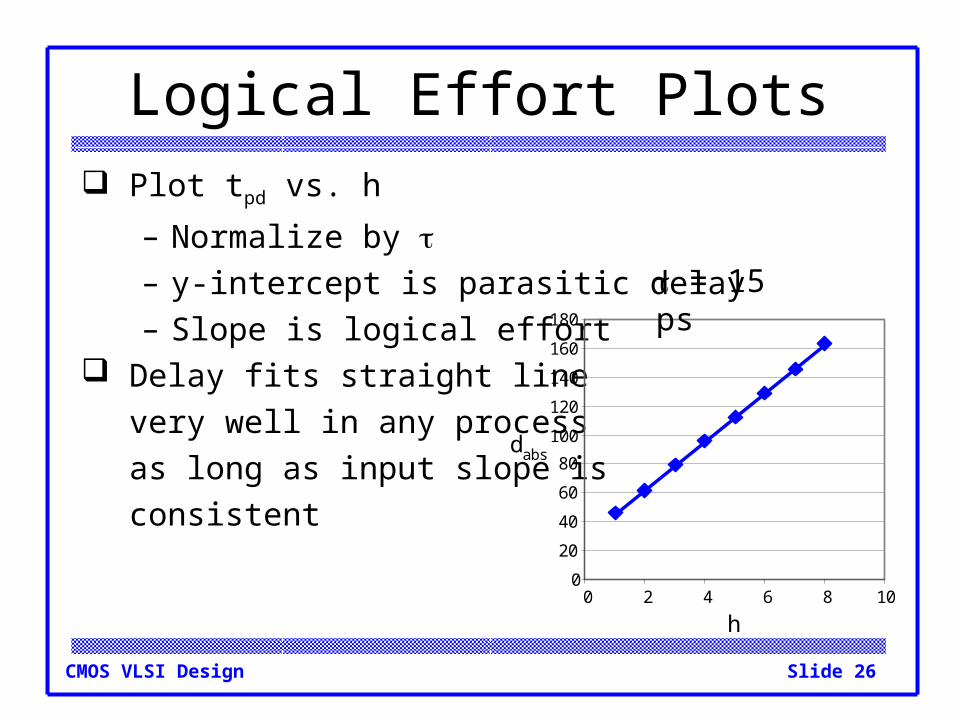
Logical Effort Plots Plot tpd vs. h
– Normalize by – y-intercept is parasitic delay– Slope is logical effort
Delay fits straight line
very well in any process
as long as input slope is
consistent
0
20
40
60
80
100
120
140
160
180
0 2 4 6 8 10
h
dabs
= 15 ps

Slide 27CMOS VLSI Design
Logical Effort Data For NAND gates in TSMC 180 nm process:
Notes:– Parasitic delay is greater for outer input– Average logical effort is better than estimated

Slide 28CMOS VLSI Design
Comparison