Embed Size (px)
Citation preview

EECS 247 Lecture 3: Filters © 2009 H.K. Page 1
EE247Administrative
• Due to office hour conflict with EE142 class:– New office hours:
• Tues: 4 to 5pm (same as before)• Wed.: 10:30 to 11:30am (new)• Thurs.: no office hours
– Office hours held @ 567 Cory Hall
EECS 247 Lecture 3: Filters © 2009 H.K. Page 2
EE247Course Reading Material
• Note that the class website includes a section named: Reading Material including:
• List of books (on reserve in the library)• List of articles (as pdf files):
– Articles for Filters – Articles for Nyquist Rate Data Converters – Articles for Oversampled Data Converters
– You will be asked to read some of the articles and answer questions
– If you plan to embark on a career in Mixed Signal Circuit Design consider reading all the publications listed

EECS 247 Lecture 3: Filters © 2009 H.K. Page 3
EE247 Lecture 3
• Active Filters– Active biquads
• How to build higher order filters?• Integrator-based filters
– Signal flowgraph concept– First order integrator-based filter– Second order integrator-based filter & biquads
– High order & high Q filters• Cascaded biquads & first order filters
– Cascaded biquad sensitivity to component mismatch• Ladder type filters
EECS 247 Lecture 3: Filters © 2009 H.K. Page 4
Higher-Order Filters in the Integrated Form
• One way of building higher-order filters (n>2) is via cascade of 2nd
order biquads & 1st order , e.g. Sallen-Key,or Tow-Thomas, & RC
2nd orderFilter ……
Nx 2nd order sections Filter order: n=2N
1 2 Ν
Cascade of 1st and 2nd order filters:☺ Easy to implement
Highly sensitive to component mismatch -good for low Q filters only
For high Q applications good alternative: Integrator-based ladder filters
2nd orderFilter
1st or 2nd orderFilter
EECS 247 Lecture 3: Filters © 2009 H.K. Page 5
Integrator Based Filters• Main building block for this category of filters
Integrator• By using signal flowgraph techniques
Conventional RLC filter topologies can be converted to integrator based type filters
• How to design integrator based filters?– Introduction to signal flowgraph techniques– 1st order integrator based filter– 2nd order integrator based filter– High order and high Q filters
EECS 247 Lecture 3: Filters © 2009 H.K. Page 6
What is a Signal Flowgraph (SFG)?
• SFG Topological network representation consisting of nodes & branches- used to convert one form of network to a more suitable form (e.g. passive RLC filters to integrator based filters)
• Any network described by a set of linear differential equations can be expressed in SFG form
• For a given network, many different SFGs exists
• Choice of a particular SFG is based on practical considerations such as type of available components
*Ref: W.Heinlein & W. Holmes, “Active Filters for Integrated Circuits”, Prentice Hall, Chap. 8, 1974.

EECS 247 Lecture 3: Filters © 2009 H.K. Page 7
What is a Signal Flowgraph (SFG)?• Signal flowgraph technique consist of nodes & branches:
– Nodes represent variables (V & I in our case) – Branches represent transfer functions (we will call the
transfer function branch multiplication factor or BMF)• To convert a network to its SFG form, KCL & KVL is used to
derive state space description• Simple example:
Circuit State-space description SFG
ZZ
VoinIinI
VoI Z Vin o× =
EECS 247 Lecture 3: Filters © 2009 H.K. Page 8
Signal Flowgraph (SFG)Examples
1SL
Circuit State-space description SFG
R
L
R
oV
C 1SC
Vin
Vo
oI
VoinI
inI
inI
inI Vo
Vin oI
I R Vin o
1V Iin o
SL
1I Vin o
SC
× =
× =
× =
EECS 247 Lecture 3: Filters © 2009 H.K. Page 9
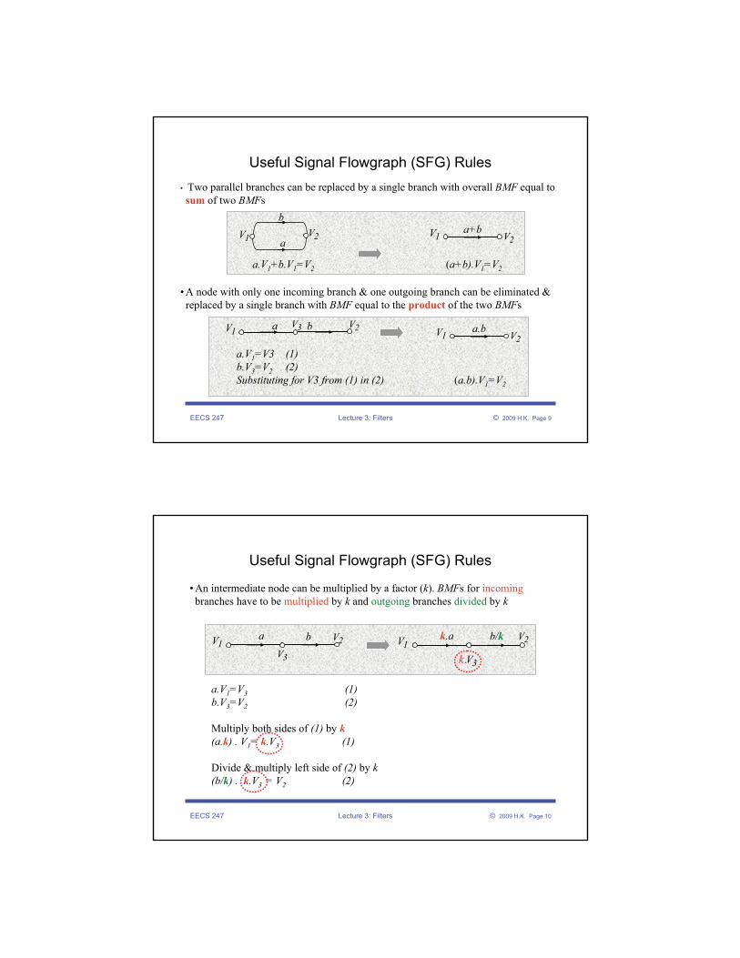
Useful Signal Flowgraph (SFG) Rules
1Va
2Vb
a+b1V
2V
a.b1V
2V3Va b1V 2V
a.V1+b.V1=V2 (a+b).V1=V2
a.V1=V3 (1)b.V3=V2 (2)Substituting for V3 from (1) in (2) (a.b).V1=V2
• Two parallel branches can be replaced by a single branch with overall BMF equal to sum of two BMFs
• A node with only one incoming branch & one outgoing branch can be eliminated & replaced by a single branch with BMF equal to the product of the two BMFs
EECS 247 Lecture 3: Filters © 2009 H.K. Page 10
Useful Signal Flowgraph (SFG) Rules
• An intermediate node can be multiplied by a factor (k). BMFs for incomingbranches have to be multiplied by k and outgoing branches divided by k
3V
a b1V 2V k.a b/k
1V 2V
3.Vk
a.V1=V3 (1)b.V3=V2 (2)
Multiply both sides of (1) by k(a.k) . V1= k.V3 (1)
Divide & multiply left side of (2) by k(b/k) . k.V3 = V2 (2)

EECS 247 Lecture 3: Filters © 2009 H.K. Page 11
Useful Signal Flowgraph (SFG) Rules
hiV2V a
oV
b
g-b
3VhiV
2V a/(1+b)oV
b
g
3V
3VciV
2V aoV
b
d-bciV2V a
oV-1 -b
1 d
3V
• Simplifications can often be achieved by shifting or eliminating nodes• Example: eliminating node V4
• A self-loop branch with BMF y can be eliminated by multiplying the BMFof incoming branches by 1/(1-y)
V4
EECS 247 Lecture 3: Filters © 2009 H.K. Page 12
Integrator Based Filters1st Order LPF
• Conversion of simple lowpass RC filter to integrator-based type by using signal flowgraph techniques
in
V 1os CV 1 R
=+
oV
RsCinV

EECS 247 Lecture 3: Filters © 2009 H.K. Page 13
What is an Integrator?Example: Single-Ended Opamp-RC Integrator
∫inVoV
C
inV
-
+R -
Note: Practical integrator in CMOS technology has input & output both in the form of voltage and not current Consideration for SFG derivation
oV
RCτ =
a ≈ ∞
in sC ,o o in o inV 1 1V V V , V V dtR sRC RC
= − = = − × = − ∫
EECS 247 Lecture 3: Filters © 2009 H.K. Page 14
Integrator Based Filters1st Order LPF
1. Start from circuit prototype-Name voltages & currents for all components
2. Use KCL & KVL to derive state space description in such a way to have BMFs in the integrator form:
Capacitor voltage expressed as function of its current VCap.=f(ICap.)Inductor current as a function of its voltage IInd.=f(VInd.)
3. Use state space description to draw signal flowgraph (SFG) (see next page)
1IoV
RsCinV
2I
1V+ −
CV
+
−

EECS 247 Lecture 3: Filters © 2009 H.K. Page 15
Integrator Based FiltersFirst Order LPF
1IoV
1
RsCinV
2I
1V+ −
1Rs
1sC
2I1I
CVinV 1−1 1V
• All voltages & currents nodes of SFG
• Voltage nodes on top, corresponding current nodes below each voltage node
SFG
CV
+
−
oV1
Integrator formV V V1 in C
1V IC 2 sCV Vo C
1I V1 1 RsI I2 1
= −
= ×
=
= ×
=
EECS 247 Lecture 3: Filters © 2009 H.K. Page 16
Normalize• Since integrators are the main building blocks require in & out signals
in the form of voltage (not current)
Convert all currents to voltages by multiplying current nodes by a scaling resistance R*
Corresponding BMFs should then be scaled accordingly
1 in o
11
2o
2 1
V V VV
IRsI
VsC
I I
=
=
= −
=
1 in o*
*1 1
*2
o *
* *2 1
V V V
RI R V
Rs
I RV
sC R
I R I R
=
=
= −
=
* 'x xI R V=
1 in o*
'1 1
'2
o *
' '2 1
V V V
RV V
Rs
VV
sC R
V V
=
=
= −
=
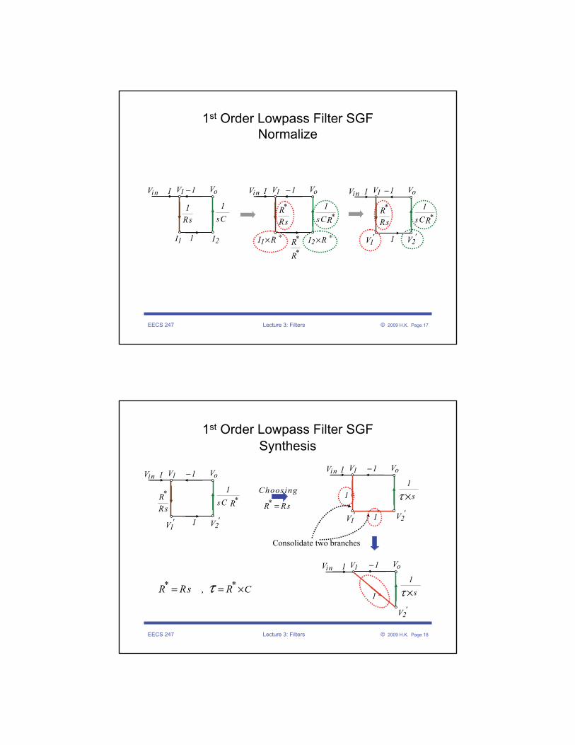
EECS 247 Lecture 3: Filters © 2009 H.K. Page 17
1st Order Lowpass Filter SGFNormalize
'2V
*1
sCR
oVinV 1−1 1V
1
*RRs
1Rs
1sC
2I1I
oVinV 1−1
1
1V
'1V
oVinV 1−1 1V
*RRs
1I R ∗× 2I R ∗×
*1
sCR
*
*R
R
EECS 247 Lecture 3: Filters © 2009 H.K. Page 18
1st Order Lowpass Filter SGFSynthesis
'1V
1*1
sC R
oVinV 1−1 1V
'2V1
*RRs
* * CR Rs , Rτ= = ×
'1V
1sτ ×
oVinV 1−1 1V
'2V1
1sτ ×
oVinV 1−1 1V
'2V
1
Consolidate two branches
*Choosing
R Rs=
EECS 247 Lecture 3: Filters © 2009 H.K. Page 19
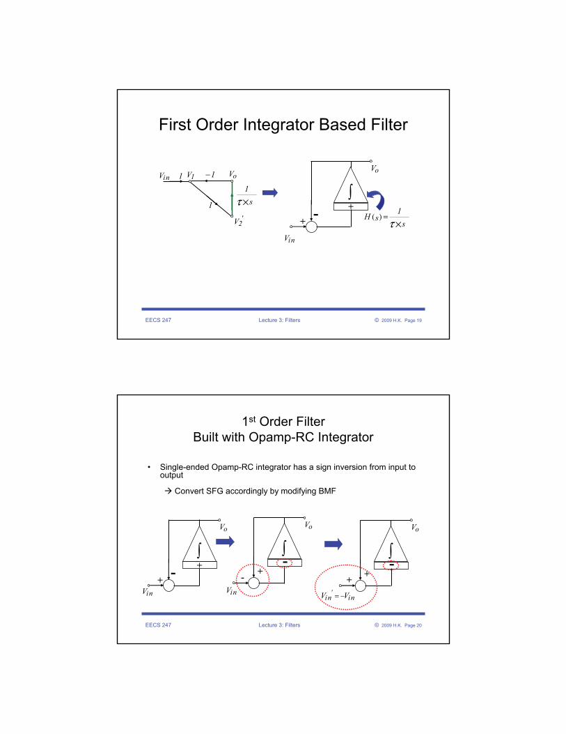
First Order Integrator Based Filter
oV
inV
-+ ( )1
H ssτ
=×
∫+
1sτ ×
oVinV 1−1 1V
'2V
1
EECS 247 Lecture 3: Filters © 2009 H.K. Page 20
1st Order Filter Built with Opamp-RC Integrator
oV
inV
-+
∫+
• Single-ended Opamp-RC integrator has a sign inversion from input to output
Convert SFG accordingly by modifying BMF
oV
inV-
∫+
-
oV
'in inV V= −
+
∫+
-

EECS 247 Lecture 3: Filters © 2009 H.K. Page 21
1st Order Filter Built with Opamp-RC Integrator
• To avoid requiring an additional opamp to perform summation at the input node:
oV
'in inV V= −
+
∫+
-
oV
'inV
∫--
EECS 247 Lecture 3: Filters © 2009 H.K. Page 22
1st Order Filter Built with Opamp-RC Integrator (continued)
o'
in
V 11 sRCV
= −+
oV
C
in'V
-
+R
R
--
oV'
inV
∫
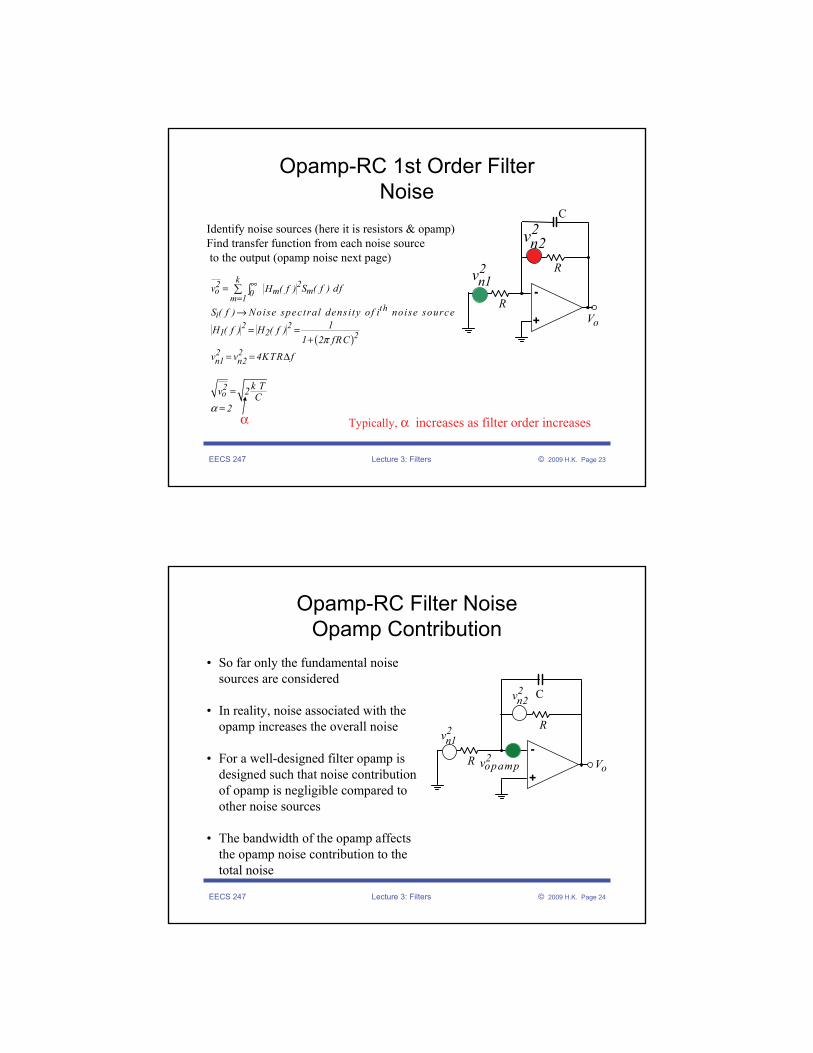
EECS 247 Lecture 3: Filters © 2009 H.K. Page 23
Opamp-RC 1st Order Filter Noise
2n1v
( )
k 22o mm0m 1
thi
2 21 2 2
2 2n1 n2
2o
v S ( f ) dfH ( f )
S ( f ) Noise spec tral densi ty of i noise source1H ( f ) H ( f )
1 2 fRCv v 4KTR f
k Tv 2 C2
π
α
∞=
=
→
= =+
= = Δ
=
=
∑ ∫
oV
C
-
+R
R
Typically, α increases as filter order increases
Identify noise sources (here it is resistors & opamp)Find transfer function from each noise sourceto the output (opamp noise next page)
2n2v
α
EECS 247 Lecture 3: Filters © 2009 H.K. Page 24
Opamp-RC Filter NoiseOpamp Contribution
2n1v
2opampv oV
C
-
+R
R
• So far only the fundamental noise sources are considered
• In reality, noise associated with the opamp increases the overall noise
• For a well-designed filter opamp is designed such that noise contribution of opamp is negligible compared to other noise sources
• The bandwidth of the opamp affects the opamp noise contribution to the total noise
2n2v

EECS 247 Lecture 3: Filters © 2009 H.K. Page 25
Integrator Based Filter2nd Order RLC Filter
oV
1
1sL
R CinI•State space description:
R L C o
CC
RR
LL
C in R L
V V V VI
VsC
VI
RV
IsL
I I I I
=
=
= = =
=
= − −
• Draw signal flowgraph (SFG)
SFG
L
1R
1sC
CIRI
CV
inI
1−1
RV 1
1−
LV
LI
CV
LI
+
- CILV
+
-
Integrator form
+
-RV
RI
EECS 247 Lecture 3: Filters © 2009 H.K. Page 26
1 1
*RR *
1sCR
'1V
2V
inV
1−1
1V
*RsL
1−
oV
'3V
2nd Order RLC Filter SGFNormalize
1
1R
1sC
CIRI
CV
inI
1−1
RV 1
1−
LV
LI
1sL
• Convert currents to voltages by multiplying all current nodes by the scaling resistance R*
* 'x xI R V=
'2V
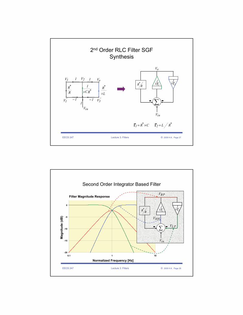
EECS 247 Lecture 3: Filters © 2009 H.K. Page 27
inV
1*R R 21
sτ11
sτ1 1
*RR *
1sCR
'1V
2V
inV
1−1
1V
*RsL
1−
oV
'3V
2nd Order RLC Filter SGFSynthesis
∑
oV
--
* *1 2R C L Rτ τ= × =
EECS 247 Lecture 3: Filters © 2009 H.K. Page 28
-20
-15
-10
-5
0
0.1 1 10
Second Order Integrator Based Filter
Normalized Frequency [Hz]
Mag
nitu
de (d
B)
inV
1*R R 21
sτ11
sτ
BPV
-- LPV
HPV
∑
Filter Magnitude Response

EECS 247 Lecture 3: Filters © 2009 H.K. Page 29
Second Order Integrator Based Filter
inV
1*R R 21
sτ11
sτ
BPV
-- LPV
HPV
∑
BP 22in 1 2 2
LP2in 1 2 2
2HP 1 2
2in 1 2 2* *
1 2*
0 1 2
1 2
1 2 *
V sV s s 1V 1V s s 1V sV s s 1
R C L R
R R11
Q 1
From matching pointof v iew desirable :RQ
R
L C
β
β
β
β
β
ττ τ τ
τ τ ττ τ
τ τ τ
ω τ τ
τ τ
τ τ
τ τ
=+ +
=+ +
=+ +
= × =
=
= =
= ×
= → =
EECS 247 Lecture 3: Filters © 2009 H.K. Page 30
Second Order Bandpass Filter Noise
2 2n1 n2
2o
v v 4KTRdf
k Tv 2 Q C
= =
=
inV
1*R R2
1sτ
11
sτ
BPV
--
2n1v
2n2v
• Find transfer function of each noise source to the output
• Integrate contribution of all noise sources
• Here it is assumed that opamps are noise free (not usually the case!)
k 22o mm0m 1
v S ( f ) dfH ( f )∞=
= ∑ ∫
Typically, α increases as filter order increasesNote the noise power is directly proportion to Qα
∑
EECS 247 Lecture 3: Filters © 2009 H.K. Page 31
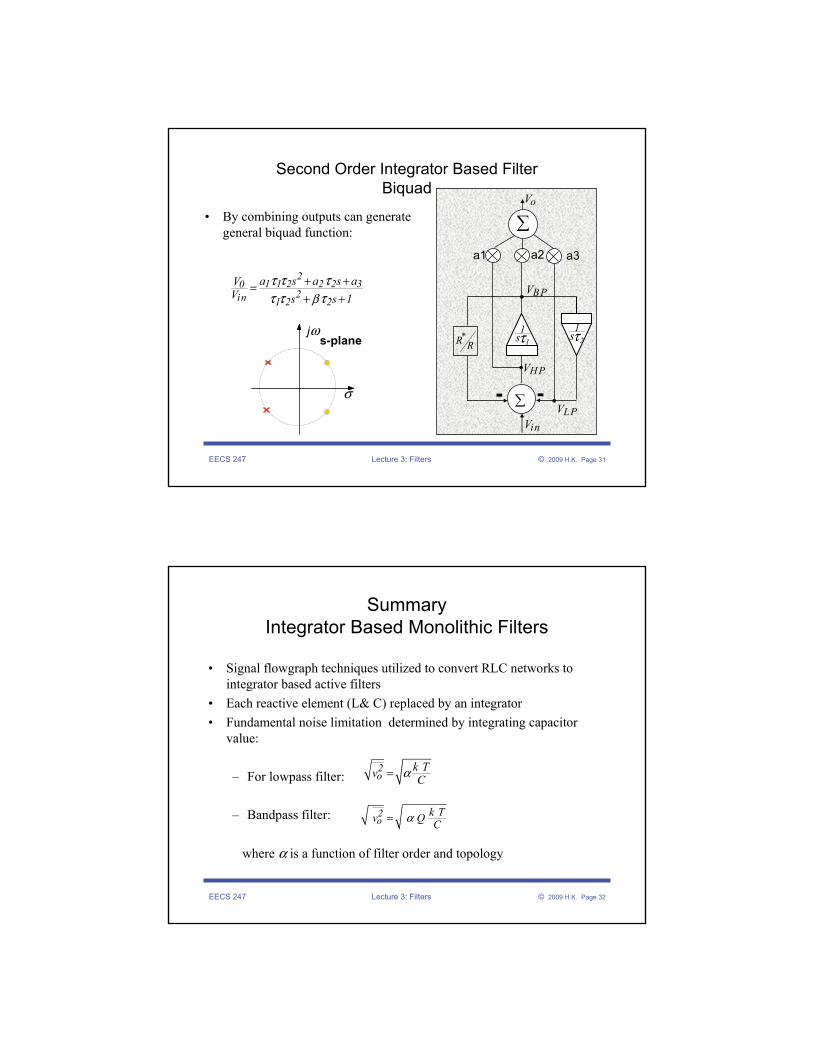
Second Order Integrator Based FilterBiquad
inV
1*R R 21
sτ11
sτ
BPV
--
21 1 2 2 2 30
2in 1 2 2
a s a s aVV s s 1β
τ τ ττ τ τ
+ +=+ +
∑oV
∑
a1 a2 a3
HPV
LPV
• By combining outputs can generate general biquad function:
s-planejω
σ
EECS 247 Lecture 3: Filters © 2009 H.K. Page 32
SummaryIntegrator Based Monolithic Filters
• Signal flowgraph techniques utilized to convert RLC networks to integrator based active filters
• Each reactive element (L& C) replaced by an integrator• Fundamental noise limitation determined by integrating capacitor
value:
– For lowpass filter:
– Bandpass filter:
where α is a function of filter order and topology
2o
k Tv Q Cα=
2o
k Tv Cα=

EECS 247 Lecture 3: Filters © 2009 H.K. Page 33
Higher Order Filters• How do we build higher order filters?
– Cascade of biquads and 1st order sections• Each complex conjugate pole built with a biquad and real pole
with 1st order section• Easy to implement• In the case of high order high Q filters highly sensitive to
component mismatch– Direct conversion of high order ladder type RLC filters
• SFG techniques used to perform exact conversion of ladder type filters to integrator based filters
• More complicated conversion process• Much less sensitive to component mismatch compared to cascade
of biquads
EECS 247 Lecture 3: Filters © 2009 H.K. Page 34
Higher Order FiltersCascade of Biquads
Example: LPF filter for CDMA cell phone baseband receiver • LPF with
– fpass = 650 kHz Rpass = 0.2 dB– fstop = 750 kHz Rstop = 45 dB– Assumption: Can compensate for phase distortion in the digital domain
• Matlab used to find minimum order required 7th order Elliptic Filter
• Implementation with cascaded BiquadsGoal: Maximize dynamic range– Pair poles and zeros– In the cascade chain place lowest Q poles first and progress to higher Q
poles moving towards the output node
EECS 247 Lecture 3: Filters © 2009 H.K. Page 35
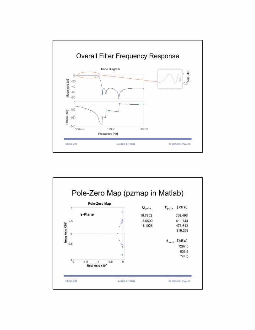
Overall Filter Frequency Response
Bode DiagramP
hase
(deg
)M
agni
tude
(dB
)
-80
-60
-40
-20
0
-540
-360
-180
0
Frequency [Hz]300kHz 1MHz
Mag
. (dB
)
-0.2
0
3MHz
EECS 247 Lecture 3: Filters © 2009 H.K. Page 36
Pole-Zero Map (pzmap in Matlab)
Qpole fpole [kHz]
16.7902 659.4963.6590 611.7441.1026 473.643
319.568
fzero [kHz]
1297.5836.6744.0
Pole-Zero Map
-2 -1.5 -1 -0.5 0-1
-0.5
0
0.5
1
Imag
Axi
s X1
07
Real Axis x107
s-Plane
EECS 247 Lecture 3: Filters © 2009 H.K. Page 37
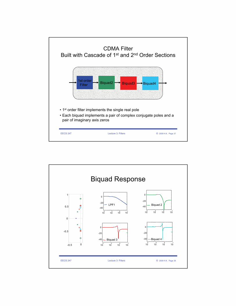
CDMA FilterBuilt with Cascade of 1st and 2nd Order Sections
• 1st order filter implements the single real pole• Each biquad implements a pair of complex conjugate poles and a
pair of imaginary axis zeros
1st orderFilter Biquad2 Biquad4 Biquad3
EECS 247 Lecture 3: Filters © 2009 H.K. Page 38
Biquad Response
104
105
106
107
-40
-20
0
LPF1
-0.5 0
-0.5
0
0.5
1
104
105
106
107
-40
-20
0
Biquad 2
104
105
106
107
-40
-20
0
Biquad 3
104
105
106
107
-40
-20
0
Biquad 4

EECS 247 Lecture 3: Filters © 2009 H.K. Page 39
Individual Stage Magnitude Response
Frequency [Hz]
Mag
nitu
de (d
B)
104 105 106 107-50
-40
-30
-20
-10
0
10
LPF1Biquad 2Biquad 3Biquad 4
-0.5 0
-0.5
0
0.5
1
EECS 247 Lecture 3: Filters © 2009 H.K. Page 40
Intermediate Outputs
Frequency [Hz]
Mag
nitu
de (d
B)
-80
-60
-40
-20
Mag
nitu
de (d
B)
LPF1 +Biquad 2
Mag
nitu
de (d
B)
Biquads 1, 2, 3, & 4
Mag
nitu
de (d
B)
-80
-60
-40
-20
0
LPF10
10kHz10
6
-80
-60
-40
-20
0
100kHz 1MHz 10MHz
5 6 7
-80
-60
-40
-20
0
4 5 6
Frequency [Hz]
10kHz10
100kHz 1MHz 10MHz
LPF1 +Biquads 2,3 LPF1 +Biquads 2,3,4
EECS 247 Lecture 3: Filters © 2009 H.K. Page 41
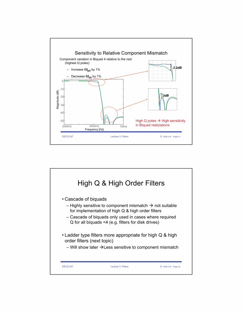
-10
Sensitivity to Relative Component MismatchComponent variation in Biquad 4 relative to the rest
(highest Q poles):
– Increase ωp4 by 1%
– Decrease ωz4 by 1%
High Q poles High sensitivityin Biquad realizations
Frequency [Hz]1MHz
Mag
nitu
de (d
B)
-30
-40
-20
0
200kHz
3dB
600kHz
-50
2.2dB
EECS 247 Lecture 3: Filters © 2009 H.K. Page 42
High Q & High Order Filters
• Cascade of biquads– Highly sensitive to component mismatch not suitable
for implementation of high Q & high order filters– Cascade of biquads only used in cases where required
Q for all biquads <4 (e.g. filters for disk drives)
• Ladder type filters more appropriate for high Q & high order filters (next topic)– Will show later Less sensitive to component mismatch

EECS 247 Lecture 3: Filters © 2009 H.K. Page 43
Ladder Type Filters
• Active ladder type filters – For simplicity, will start with all pole ladder type filters
• Convert to integrator based form- example shown– Then will attend to high order ladder type filters
incorporating zeros• Implement the same 7th order elliptic filter in the form of
ladder RLC with zeros– Find level of sensitivity to component mismatch – Compare with cascade of biquads
• Convert to integrator based form utilizing SFG techniques– Effect of integrator non-Idealities on filter frequency
characteristics
EECS 247 Lecture 3: Filters © 2009 H.K. Page 44
RLC Ladder FiltersExample: 5th Order Lowpass Filter
• Made of resistors, inductors, and capacitors• Doubly terminated or singly terminated (with or w/o RL)
RsC1 C3
L2
C5
L4
inV RL
oV
Doubly terminated LC ladder filters Lowest sensitivity to component mismatch

EECS 247 Lecture 3: Filters © 2009 H.K. Page 45
LC Ladder Filters
• First step in the design process is to find values for Ls and Csbased on specifications:– Filter graphs & tables found in:
• A. Zverev, Handbook of filter synthesis, Wiley, 1967.• A. B. Williams and F. J. Taylor, Electronic filter design, 3rd edition, McGraw-
Hill, 1995.– CAD tools
• Matlab• Spice
RsC1 C3
L2
C5
L4
inV RL
oV
EECS 247 Lecture 3: Filters © 2009 H.K. Page 46
LC Ladder Filter Design Example
Design a LPF with maximally flat passband:f-3dB = 10MHz, fstop = 20MHzRs >27dB @ fstop
• Maximally flat passband Butterworth
From: Williams and Taylor, p. 2-37
Stopband A
ttenuation
Νοrmalized ω
• Find minimum filter order :
• Here standard graphs from filter books are used
fstop / f-3dB = 2Rs >27dB
Minimum Filter Order5th order Butterworth
1
-3dB
2
-30dB
Pas
sban
d At
tenu
atio
n
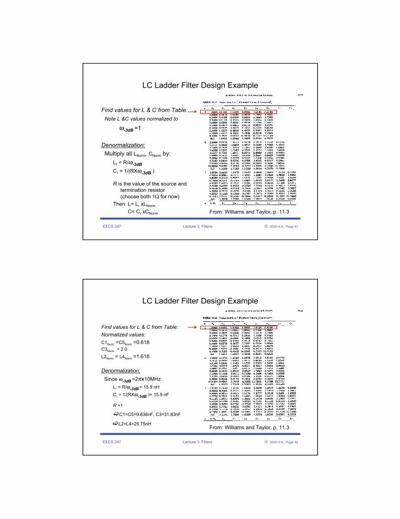
EECS 247 Lecture 3: Filters © 2009 H.K. Page 47
LC Ladder Filter Design Example
From: Williams and Taylor, p. 11.3
Find values for L & C from Table:Note L &C values normalized to
ω-3dB =1
Denormalization:Multiply all LNorm, CNorm by:
Lr = R/ω-3dBCr = 1/(RXω-3dB )
R is the value of the source and termination resistor (choose both 1Ω for now)
Then: L= Lr xLNorm
C= Cr xCNorm
EECS 247 Lecture 3: Filters © 2009 H.K. Page 48
LC Ladder Filter Design Example
From: Williams and Taylor, p. 11.3
Find values for L & C from Table:Normalized values:C1Norm =C5Norm =0.618C3Norm = 2.0L2Norm = L4Norm =1.618
Denormalization:Since ω-3dB =2πx10MHz
Lr = R/ω-3dB = 15.9 nHCr = 1/(RXω-3dB )= 15.9 nF
R =1
C1=C5=9.836nF, C3=31.83nF
L2=L4=25.75nH
EECS 247 Lecture 3: Filters © 2009 H.K. Page 49
Last Lecture:Example: 5th Order Butterworth Filter
Rs=1ΩC19.836nF
C331.83nF
L2=25.75nH
C59.836nF
L4=25.75nH
inV RL=1Ω
oV
Specifications:f-3dB = 10MHz, fstop = 20MHzRs >27dB
Used filter tables to obtain Ls & Cs
Frequency [MHz]
Mag
nitu
de (d
B)
0 10 20 30-50
-40
-30
-20
-10-50
-6 dB passband attenuationdue to double termination
30dB
SPICE simulation Results
EECS 247 Lecture 3: Filters © 2009 H.K. Page 50
Low-Pass RLC Ladder FilterConversion to Integrator Based Active Filter
1I2V
RsC1 C3
L2
C5
L4
inV RL
4V 6V
3I 5I
2I4I 6I 7I
• To convert RLC ladder prototype to integrator based filer:Use Signal Flowgraph technique
Name currents and voltages for all componentsUse KCL & KVL to derive equationsMake sure reactive elements expressed as 1/s terms V(C ) =f(I) & I(L)=f(V)
Use state-space description to derive the SFGModify & simply the SFG for implementation with
integrators e.g. convert all current nodes to voltage
1V+ − 3V+ − 5V+ −oV

EECS 247 Lecture 3: Filters © 2009 H.K. Page 51
Low-Pass RLC Ladder FilterConversion to Integrator Based Active Filter
1I2V
RsC1 C3
L2
C5
L4
inV RL
4V 6V
3I 5I
2I4I 6I
• Use KCL & KVL to derive equations:
1V+ − 3V+ − 5V+ −oV
1 in 2
1 31 3
25 6
5 74
I2V V V , V , V V V2 3 2 4sC1I I4 6V , V V V , V V V4 5 4 6 6 o 6sC sC3 5
V VI , I I I , I2 1 3Rs sL
V VI I I , I , I I I , I4 3 5 6 5 7sL RL
= − = = −
= = − = =
= = − =
= − = = − =
7I
EECS 247 Lecture 3: Filters © 2009 H.K. Page 52
Low-Pass RLC Ladder FilterSignal Flowgraph
SFG
1Rs 1
1sC
2I1I
2VinV 1−1
1
1V oV1− 11
3
1sC 5
1sC2
1sL 4
1sL
1RL
1− 1− 1−1 1
1− 13V 4V 5V 6V
3I 5I4I 6I 7I
1 in 2
1 31 3
25 6
5 74
I2V V V , V , V V V2 3 2 4sC1I I4 6V , V V V , V V V4 5 4 6 6 o 6sC sC3 5
V VI , I I I , I2 1 3Rs sL
V VI I I , I , I I I , I4 3 5 6 5 7sL RL
= − = = −
= = − = =
= = − =
= − = = − =

EECS 247 Lecture 3: Filters © 2009 H.K. Page 53
Low-Pass RLC Ladder FilterSignal Flowgraph
SFG
1Rs 1
1sC
2I1I
2VinV 1−1
1
1V oV1− 11
3
1sC 5
1sC2
1sL 4
1sL
1RL
1− 1− 1−1 1
1− 13V 4V 5V 6V
3I 5I4I 6I 7I
1I2V
RsC1 C3
L2
C5
L4
inV RL
4V 6V
3I 5I
2I4I 6I
7I1V+ − 3V+ − 5V+ −
EECS 247 Lecture 3: Filters © 2009 H.K. Page 54
Low-Pass RLC Ladder FilterNormalize
1
1
*RRs
*1
1sC R
'1V
2VinV 1−1 1V oV1− 1
*
2
RsL
1− 1− 1−1 1
1− 13V 4V 5V 6V
'3V'2V '
4V '5V '
6V '7V
*3
1sC R
*
4
RsL
*5
1sC R
*RRL
1Rs 1
1sC
2I1I
2VinV 1−1
1
1V oV1− 11
3
1sC 5
1sC2
1sL 4
1sL
1RL
1− 1− 1−1 1
1− 13V 4V 5V 6V
3I 5I4I 6I 7I

EECS 247 Lecture 3: Filters © 2009 H.K. Page 55
Low-Pass RLC Ladder FilterSynthesize
1
1
1
*RRs
*1
1sC R
'1V
2VinV 1−1 1V oV1− 1
*
2
RsL
1− 1− 1−1 1
1− 13V 4V 5V 6V
'3V'2V '
4V '5V '
6V '7V
*3
1sC R
*
4
RsL
*5
1sC R
*RRL
inV
1+ -
-+ -+
+ - + -
*R Rs−
*R RL21
sτ 31
sτ 41
sτ 51
sτ11
sτ
oV2V 4V 6V
'3V '
5V
EECS 247 Lecture 3: Filters © 2009 H.K. Page 56
Low-Pass RLC Ladder FilterIntegrator Based Implementation
* * * * *2* *
L L4C C C C.R , .R , .R , .R , C .R11 2 2 3 3 4 4 5 5R R
τ τ τ τ τ= = = = = = =
Main building block: IntegratorLet us start to build the filter with RC& Opamp type integrator
inV
1+ -
-+ -+
+ - + -
*R Rs−
*R RL21
sτ 31
sτ 41
sτ 51
sτ11
sτ
oV2V 4V 6V
'3V '
5V
EECS 247 Lecture 3: Filters © 2009 H.K. Page 57
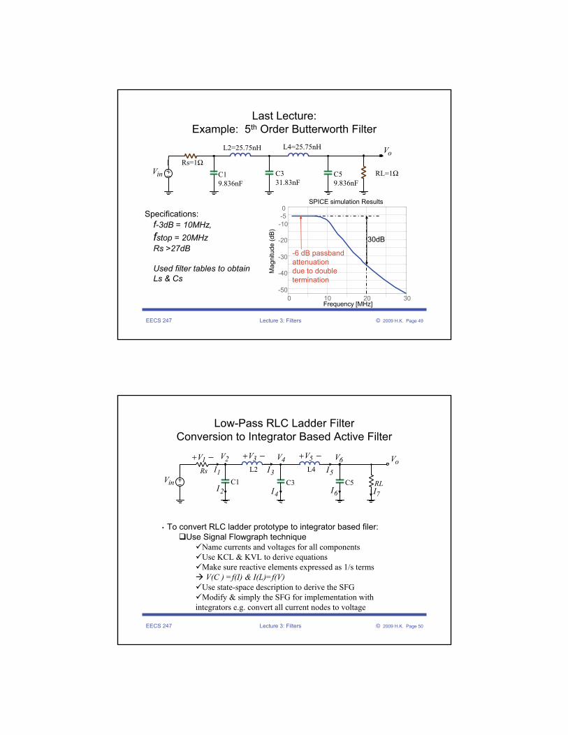
Opamp-RC Integrator
( )
( )1
2
o o in1 in1
in2 in2
1V V V VsR CI
1V VsR CI
+ − + −
+ −
− = − ×
+ − ×
oVCI
in1V-
+R1
Note: Implementation with single-ended integrator requires extra circuitry for sign inversion whereas in differential case both signal polarities are available
R2in2V
CI-
+
R1
R2
R2
R1
+-
Vin2+
Vin1+
Vin1−
Vin2−
Vo+
Vo −
Single-Ended Differential
1
2
o in1
in2
1V VsR CI
1VsR CI
= − ×
− ×
CI
EECS 247 Lecture 3: Filters © 2009 H.K. Page 58
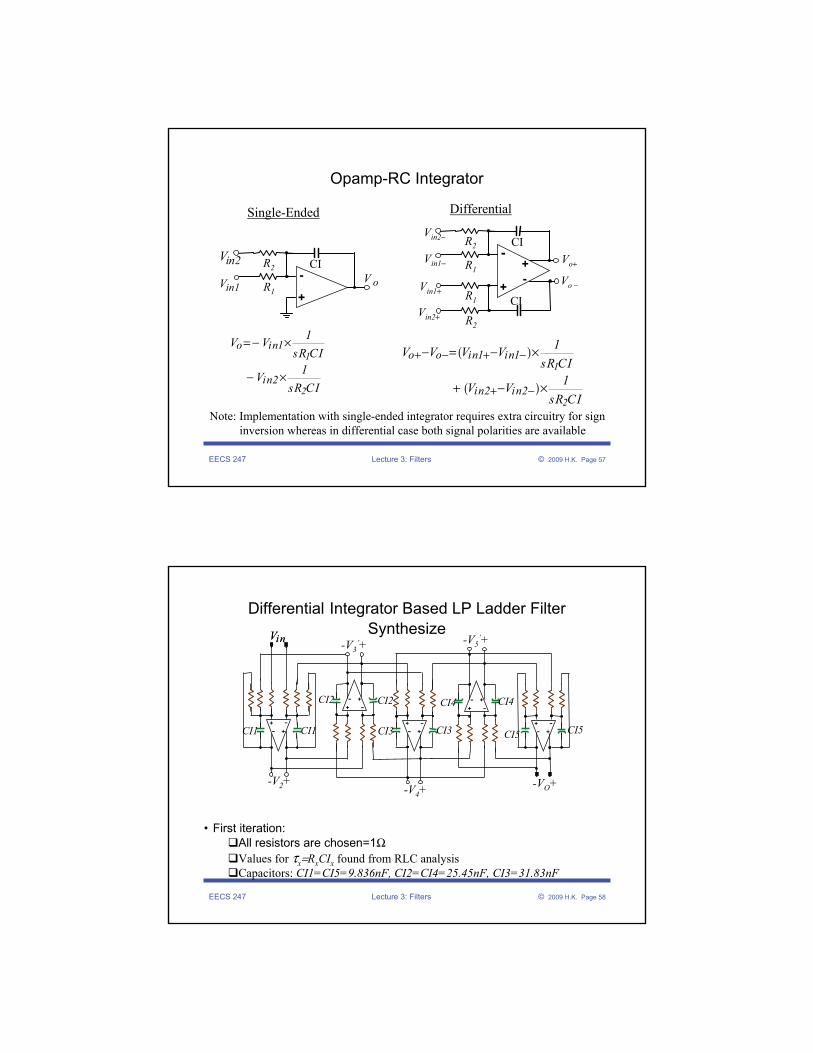
inV
Differential Integrator Based LP Ladder FilterSynthesize
• First iteration:All resistors are chosen=1ΩValues for τx=RxCIx found from RLC analysisCapacitors: CI1=CI5=9.836nF, CI2=CI4=25.45nF, CI3=31.83nF
+
+
--+
+
--
+
+--+
+--
+
+
--
inV
-V2+ -V4+-VO+
-V3’+ -V5
’+
CI1 CI1 CI3 CI3
CI2 CI2 CI4 CI4
CI5 CI5

EECS 247 Lecture 3: Filters © 2009 H.K. Page 59
Simulated Magnitude Response
oV
4V
'3V
'5V
2V
0.5
1
0.1
1
0.5
10MHz 10MHz
EECS 247 Lecture 3: Filters © 2009 H.K. Page 60
Scale Node Voltages
Scale Vo by factor “s”To maximize dynamic range
scale node voltages

EECS 247 Lecture 3: Filters © 2009 H.K. Page 61
inV
Differential Integrator Based LP Ladder FilterNode Scaling
• Second iteration:Nodes scaled, note output node x2Resistor values scaled according to scaling of nodesCapacitors the same : C1=C5=9.836nF, C2=C4=25.45nF, C3=31.83nF
+
+--
+
+--
+
+--+
+--
+
+
--
inV
VO X 2
X 2/
1.8
V4 X 1.6
V3’ X 1.2 V5
’ X 1.8
V2
X1.8
/2
X 1.
6/1.
8X 1.
8/1.
6
X 1.
2
X 1.
2/1.
6
X 1/
1.2
X 1.
6/1.
2
EECS 247 Lecture 3: Filters © 2009 H.K. Page 62
Maximizing Signal Handling by Node Voltage Scaling
Scale Vo by factor “s”
Before Node Scaling After Node Scaling
EECS 247 Lecture 3: Filters © 2009 H.K. Page 63
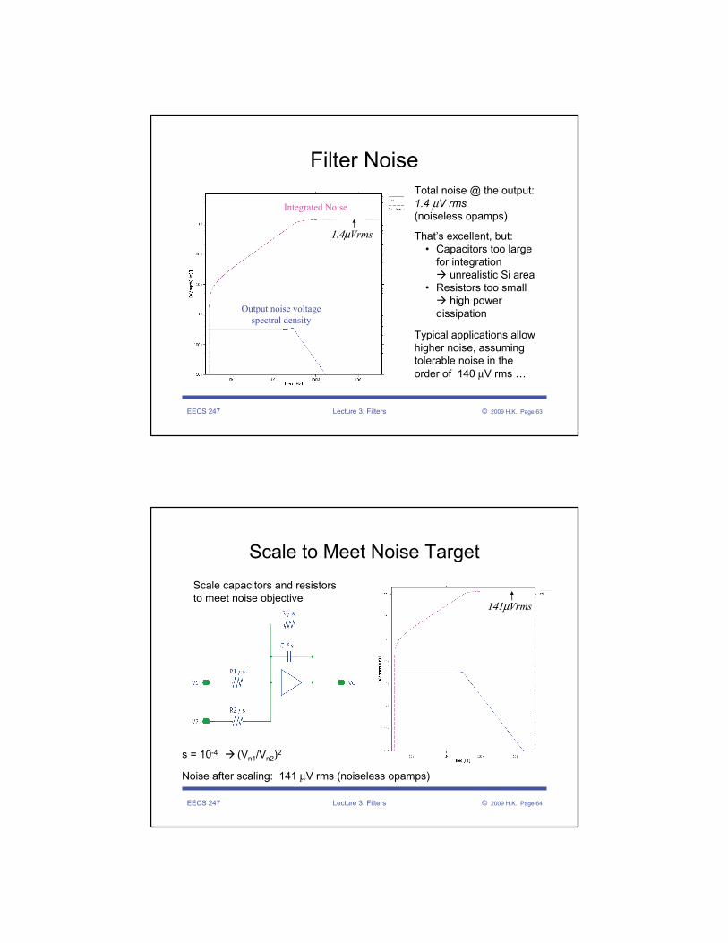
Filter NoiseTotal noise @ the output: 1.4 μV rms(noiseless opamps)
That’s excellent, but:• Capacitors too large
for integration unrealistic Si area
• Resistors too small high power
dissipation
Typical applications allow higher noise, assuming tolerable noise in the order of 140 μV rms …
Output noise voltage spectral density
Integrated Noise
1.4μVrms
EECS 247 Lecture 3: Filters © 2009 H.K. Page 64
Scale to Meet Noise TargetScale capacitors and resistors to meet noise objective
s = 10-4 (Vn1/Vn2)2
Noise after scaling: 141 μV rms (noiseless opamps)
141μVrms
EECS 247 Lecture 3: Filters © 2009 H.K. Page 65
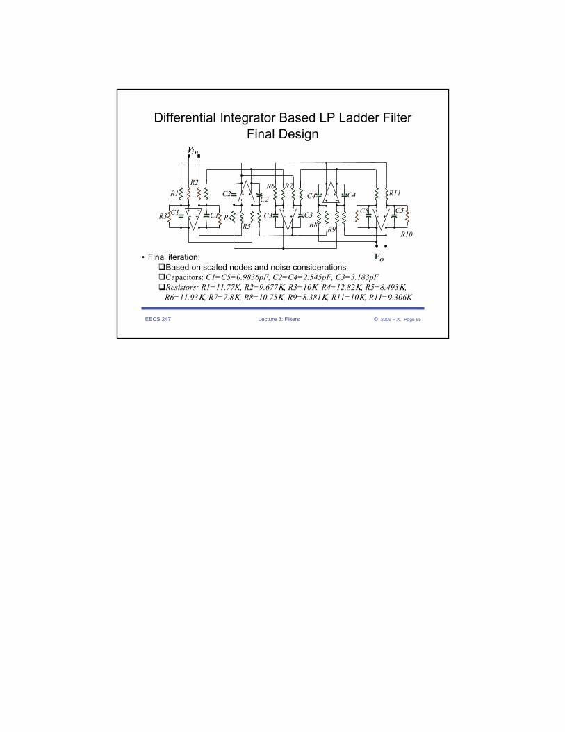
inV
Differential Integrator Based LP Ladder FilterFinal Design
• Final iteration:Based on scaled nodes and noise considerationsCapacitors: C1=C5=0.9836pF, C2=C4=2.545pF, C3=3.183pFResistors: R1=11.77K, R2=9.677Κ, R3=10Κ, R4=12.82Κ, R5=8.493Κ, R6=11.93Κ, R7=7.8Κ, R8=10.75Κ, R9=8.381Κ, R11=10Κ, R11=9.306K
+
+--
+
+--
+
+--+
+--
+
+
--
inV
VO
C1 C1 C3 C3
C2C2 C4 C4
C5 C5
R1R2
R3 R4R5
R6 R7
R8R9 R10
R11