Embed Size (px)
Citation preview

EECS 247- Lecture 18 Nyquist Rate ADCs-Sampling Networks © 2008 H.K. Page 1
EE247Lecture 18
ADC Converters– Sampling (continued)
• Sampling switch charge injection & clock feedthrough– Complementary switch– Use of dummy device– Bottom-plate switching
– Track & hold • T/H circuits• T/H combined with summing/difference function• T/H circuit incorporating gain & offset cancellation• T/H aperture uncertainty
EECS 247- Lecture 18 Nyquist Rate ADCs-Sampling Networks © 2008 H.K. Page 2
Practical SamplingIssues
vIN vOUT
CM1
φ1
• Switch induced noise due to M1 finite channel resistance• Clock jitter• Finite Rsw limited bandwidth finite acquisition time
• Rsw = f(Vin) distortion• Switch charge injection & clock feedthrough

EECS 247- Lecture 18 Nyquist Rate ADCs-Sampling Networks © 2008 H.K. Page 3
Sampling Switch Charge Injection & Clock FeedthroughSwitching from Track to Hold
Vi VO
Cs
M1
VG
• First assume Vi is a DC voltage• When switch turns off offset voltage induced on Cs• Why?
VG
t
VH
Vi
VL
Vi +Vth
VO
Vi
toff
ΔV
t
EECS 247- Lecture 18 Nyquist Rate ADCs-Sampling Networks © 2008 H.K. Page 4
SamplingSwitch Charge Injection
• Channel distributed RC network formed between G,S, and D• Channel to substrate junction capacitance distributed & voltage dependant• Drain/Source junction capacitors to substrate voltage dependant• Over-lap capacitance Cov = LDxWxCox
’ associated with G-S & G-D overlap
MOS xtor operating in triode regionCross section view
Distributed channel resistance & gate & junction capacitances
S
G
D
B
LD
L
Cov Cov
Cjdb
Cjsb
CHOLD

EECS 247- Lecture 18 Nyquist Rate ADCs-Sampling Networks © 2008 H.K. Page 5
Switch Charge Injection Slow Clock
• Slow clock clock fall time >> device speed During the period (t- to toff) current in channel discharges channel charge into low impedance signal source
• Only source of error Clock feedthrough from Cov to Cs
VG
t
VH
Vi
VL
Vi +Vth
tofft-
Device still conducting
EECS 247- Lecture 18 Nyquist Rate ADCs-Sampling Networks © 2008 H.K. Page 6
Switch Clock Feedthrough Slow Clock
VG
t
VH
Vi
VL
Vi +Vth
VO
Vi
toff
ΔV
t
D
Cov
VG
t-
Cs( )
( )
( ) ( )
( )
( )
ovi th L
ov sov
i th Ls
o i
ov ov ovo i i th L i th L
s s so i os
ov ovos th L
s s
CV V V V
C CC
V V VC
V V VC C C
V V V V V V 1 V VC C C
V V 1 V
C Cwhere ; V V V
C C
ε
ε
Δ = − + −+
≈ − + −
= + Δ⎛ ⎞
= − + − = − − −⎜ ⎟⎜ ⎟⎝ ⎠
= + +
= − = − −

EECS 247- Lecture 18 Nyquist Rate ADCs-Sampling Networks © 2008 H.K. Page 7
Switch Charge Injection & Clock Feedthrough Slow Clock- Example
VG
t
VH
Vi
VL
Vi +Vth
VO
Vi
toff
ΔV
t
Vi VO
Cs=1pF
M1
VG 10μ/0.18μ
t-
( )
' 2ov ox th L
ov
s
ovos th L
s
C 0.1 fF / C 9 fF / V 0.4V V 0
C 10 x0.1 fF /.1%
C 1pFAllowing 1 / 2LSB ADC resolut ion ~ 9bi t
CV V V 0.4mV
C
μ μ
μ με
ε
= = = =
= − = − = −
= → <
= − − = −
EECS 247- Lecture 18 Nyquist Rate ADCs-Sampling Networks © 2008 H.K. Page 8
Switch Charge Injection & Clock Feedthrough Fast Clock
VG
t
VH
Vi
VL
Vi +Vth
VO
Vi
toff
ΔV
t
Vi VO
Cs=1pF
M1VG
• Sudden gate voltage drop no gate voltage to establish current in channel channel charge has no choice but to escape out towards S & D
Qch
mQchnQch
n+m=1

EECS 247- Lecture 18 Nyquist Rate ADCs-Sampling Networks © 2008 H.K. Page 9
• For simplicity it is assumed channel charge divided equally between S & D • Source of error channel charge transfer + clock feedthrough via Cov to Cs
VG
t
VH
Vi
VL
Vi +Vth
VO
Vi
toff
ΔV
t
Switch Charge Injection & Clock FeedthroughFast Clock
Clock Fall-Time << Device Speed:
( )
( ) ( )( )
( )
( ) ( )
ov cho H L
ov s s
ox H i thovH L
ov s so i os
ox
sox H thov
os H Ls s
C 1 QV V V
C C 2 C
WC L V V VC 1V V
C C 2 CV V 1 V
1 WC Lwhere
2 CWC L V VC 1
V V VC 2 C
ε
ε
Δ = − − − ×+
− −≈ − − − ×
+= + +
= ×
−= − − − ×
EECS 247- Lecture 18 Nyquist Rate ADCs-Sampling Networks © 2008 H.K. Page 10
Switch Charge Injection & Clock FeedthroughFast Clock- Example
Vi VO
Cs=1pF
M1
VG 10μ/0.18μ
( ) ( )
ov ox th DD L2
2ox
s
ox H thovos H L
s s
fF fFC 0.1 , C 9 , V 0.4V ,V 1.8V , V 0
WLC 10 x0.18 x9 fF /1 / 2 1.6% ~ 5 bi t
C 1pF
WC L V VC 1V V V 1.8mV 14.6mV 16.4mV
C 2 C
μ μ
μ μ με
= = = = =
= = = → −
−= − − − × = − − = −
VG
t
VH
Vi
VL
Vi +Vth
VO
Vi
toff
ΔV
t

EECS 247- Lecture 18 Nyquist Rate ADCs-Sampling Networks © 2008 H.K. Page 11
Switch Charge Injection & Clock FeedthroughExample-Summary
Error function of:Clock fall time Input voltage level Source impedance Sampling capacitance size Switch size
Clock fall/rise should be controlled not to be faster (sharper) than necessary
Clock fall time
ε VOS
Clock fall time
1.6%
.1%
16mV
0.4mV
EECS 247- Lecture 18 Nyquist Rate ADCs-Sampling Networks © 2008 H.K. Page 12
Switch Charge InjectionError Reduction
• How do we reduce the error? Reduce switch size to reduce channel charge?
Reducing switch size increases τ increased distortion not a viable solutionSmall τ and small ΔV use minimum chanel length (mandated by technology)For a given technology τ x ΔV ~ constant
( )
( )
( )( )
cho
ss s
ON s
ox GS th
ox GS ths
o s ox H i th2
1 QV
2 CC T
R C ( note : kW 2C V VL
Consider the f igure of meri t (FOM):W
C V V1 CLFOM 2V C WC L V V V
FOM L
)μ
μ
μ
τ τ
τ
Δ = − ↓
= = ↑ =−
−= ≈ ×
Δ − −→ ∝
××

EECS 247- Lecture 18 Nyquist Rate ADCs-Sampling Networks © 2008 H.K. Page 13
Sampling Switch Charge Injection & Clock FeedthroughSummary
• Extra charge injected onto sampling capacitor @ switch device turn-off
–Channel charge injection–Clock feedthrough to Cs via Cov
• Issues due to charge injection & clock feedthrough:–DC offset induced on hold C–Input dependant error voltage distortion
• Solutions:–Slowing down clock edges as much as possible–Complementary switch?–Addition of dummy switches?–Bottom-plate sampling?
EECS 247- Lecture 18 Nyquist Rate ADCs-Sampling Networks © 2008 H.K. Page 14
Switch Charge Injection & Clock FeedthroughComplementary Switch
• In slow clock case if area of n & p devices widths are equal (Wn=Wp)effect of overlap capacitor for n & p devices to first order cancel (cancellation accuracy depends on matching of n & p width and overlap length LD)
• Since in CMOS technologies μn~2.5μp choice of Wn=Wp not optimal from linearity perspective (Wp>Wn preferable)
φ1φ1B
φ1
φ1B
VG
t
VH
Vi
VL
φ1 φ1B

EECS 247- Lecture 18 Nyquist Rate ADCs-Sampling Networks © 2008 H.K. Page 15
Switch Charge Injection Complementary Switch
Fast Clock
• In fast clock case To 1st order, offset due to overlap caps
cancelled for equal device widthInput voltage dependant error worse!
φ1
φ1B
VG
t
VH
Vi
VL
( )
( )
( )
ch n n ox n H i th n
th pch p p ox p i L
ch pch no
s s
o i os
n ox n p ox p
s
Q W C L V V V
VQ W C L V V
Q1 QV
2 C C
V V 1 V
1 W C L W C L2 C
ε
ε
− −
−−
−−
= − −
= − −
⎛ ⎞Δ ≈ − −⎜ ⎟⎜ ⎟
⎝ ⎠
= + +
+≈ ×
EECS 247- Lecture 18 Nyquist Rate ADCs-Sampling Networks © 2008 H.K. Page 16
Switch Charge InjectionDummy Switch
Vi
VO
Cs
t
VH
Vi
VL
VG VGB
WM2=1/2WM1
VG VGB
M1 M2
Q1 Q2
M 1 M 11 ch ov
M 2 M 22 ch ov
M 1 M 2M 2 M 1 2 1 ov ov
1Q Q Q
2
Q Q 2Q
1For W W Q Q & Q 2Q
2
≈ +
≈ +
= → = − =

EECS 247- Lecture 18 Nyquist Rate ADCs-Sampling Networks © 2008 H.K. Page 17
Switch Charge InjectionDummy Switch
Vi
VO
Cs
t
VH
Vi
VL
VG VGB
• Dummy switch same L as main switch but half W • Main device clock goes low, dummy device gate goes high dummy
switch acquires same amount of channel charge main switch needs to lose
• Effective only if exactly half of the charge stored in M1 is transferred to M2 (depends on input/output node impedance) and requires good matching between clock fall/rise
WM2=1/2WM1
VG VGB
M1 M2
Q1 Q2
EECS 247- Lecture 18 Nyquist Rate ADCs-Sampling Networks © 2008 H.K. Page 18
Switch Charge InjectionDummy Switch
Vi VOM1
VG
M2
VGB
To guarantee half of charge goes to each side create the same environment on both sides
Add capacitor equal to sampling capacitor to the other side of the switch + add fixed resistor to emulate input resistance of following circuit
Issues: Degrades sampling bandwidth
CsCs
RWM2=1/2WM1

EECS 247- Lecture 18 Nyquist Rate ADCs-Sampling Networks © 2008 H.K. Page 19
Dummy Switch Effectiveness Test
Ref: L. A. Bienstman et al, “ An Eight-Channel 8 13it Microprocessor Compatible NMOS D/A Converter with Programmable Scaling”, IEEE JSSC, VOL. SC-15, NO. 6, DECEMBER 1980
• Dummy switch W=1/2Wmain
• As Vin is increased Vc1-Vin is decreased channel charge decreased less charge injection
• Note large Lsgood device
area matching
EECS 247- Lecture 18 Nyquist Rate ADCs-Sampling Networks © 2008 H.K. Page 20
Switch Charge InjectionDifferential Sampling
Vi+
VO+
Vi-
VO-
• To 1st order, offset terms cancel• Note gain error ε still about the same• Has the advantage of better immunity to
noise coupling and cancellation of even order harmonics
φ
Cs
Cs
( )( )
( ) ( )
o o od i i id
o o i ioc ic
o i 1 os1
o i 2 os2
1 2od id id 1 2 ic os1 os2
V V V V V V
V V V VV V
2 2V V 1 V
V V 1 V
V V V V V V2
ε
ε
ε ε ε ε
+ − + −
+ − + −
+ +
− −
− = − =
+ += =
= + +
= + +
+= + + − + −
EECS 247- Lecture 18 Nyquist Rate ADCs-Sampling Networks © 2008 H.K. Page 21
Avoiding Switch Charge InjectionBottom Plate Sampling
• Switches M2 opened slightly earlier compared to M1Injected charge by the opening of M2 is constant since its GS
voltage is constant & eliminated when used differentially
• Since Cs bottom plate is already open when M1 is openedNo signal dependant charge injected on Cs
φ1VH
VL
t
φ1DVi
VO
M1
φ1D
φ1M2
Cs
EECS 247- Lecture 18 Nyquist Rate ADCs-Sampling Networks © 2008 H.K. Page 22
Flip-Around Track & Hold
vINvOUT
C
S1A
φ1D
S2
φ2
S2A
φ2
S3
φ1D
φ1 S1
vCM
• Concept based on bottom-plate sampling
φ1
φ2
φ1D
EECS 247- Lecture 18 Nyquist Rate ADCs-Sampling Networks © 2008 H.K. Page 23
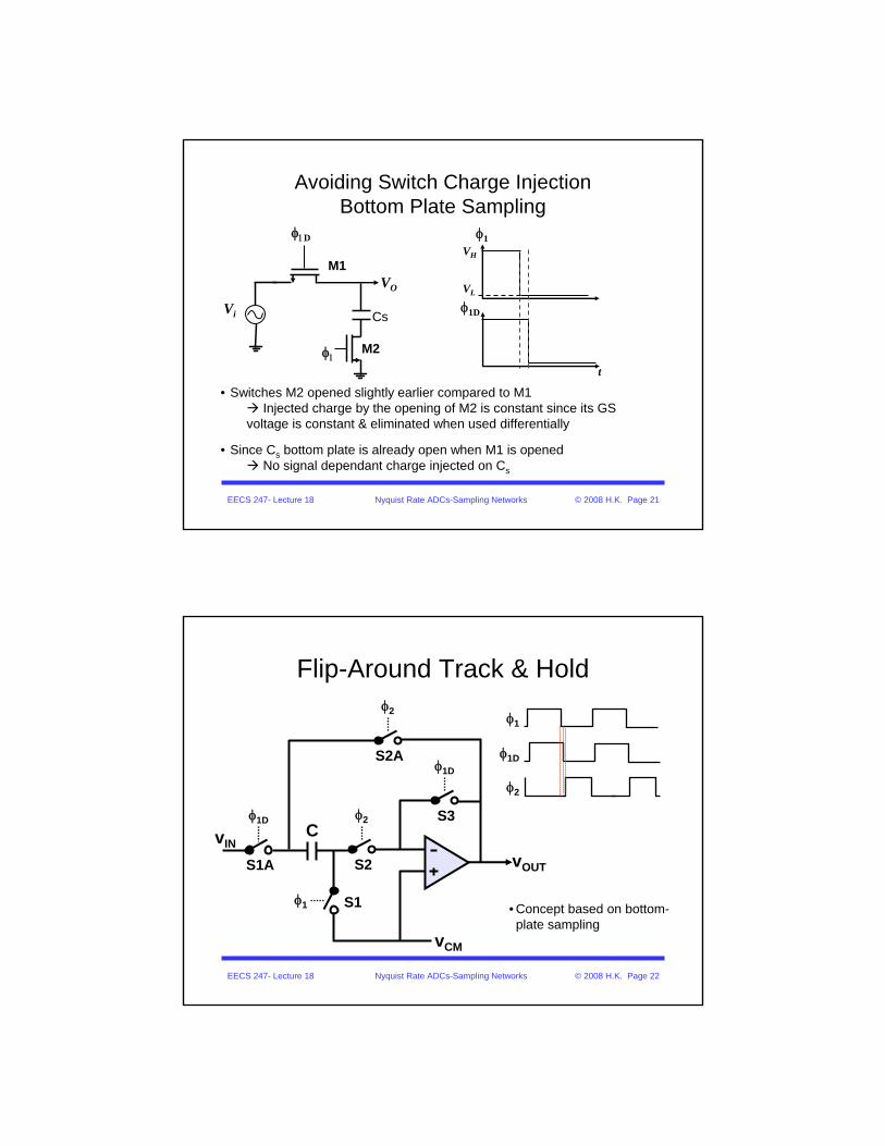
Flip-Around T/H-Basic Operationφ1 high
vIN vOUT
C
S1A
φ1D
S2
φ2
S2A
φ2
S3
φ1D
φ1 S1
vCM
Charging C
φ1
φ1D
φ2
Note: Opamp has to be stable in unity-gain configuration
Qφ1=VINxC
EECS 247- Lecture 18 Nyquist Rate ADCs-Sampling Networks © 2008 H.K. Page 24
Flip-Around T/H-Basic Operationφ2 high
vIN vOUT
C
S1A
φ1D
S2
φ2
S2A
φ2
S3
φ1D
φ1 S1
vCM
Holding
φ1
φ2
φ1D
Qφ2=VOUTxCVOUT=VIN

EECS 247- Lecture 18 Nyquist Rate ADCs-Sampling Networks © 2008 H.K. Page 25
Flip-Around T/H - Timing
S1 opens earlier than S1ANo resistive path from C bottom plate to Gnd charge can not change"Bottom Plate Sampling"
vIN
vOUT
C
S1A
φ1D
S2
φ2
S2A
φ2
S3
φ1D
φ1 S1
vCM
φ1
φ2
φ1D
EECS 247- Lecture 18 Nyquist Rate ADCs-Sampling Networks © 2008 H.K. Page 26
Charge Injection• At the instant of transitioning from track to hold
mode, some of the charge stored in sampling switch S1 is dumped onto C
• With "Bottom Plate Sampling", only charge injection component due to opening of S1 and is to first-order independent of vIN– Only a dc offset is added. This dc offset can be
removed with a differential architecture

EECS 247- Lecture 18 Nyquist Rate ADCs-Sampling Networks © 2008 H.K. Page 27
Flip-Around T/H
vIN vOUT
C
S1A
φ1D
S2
φ2
S2A
φ2
S3
φ1D
φ1 S1
vCM
Constant switch VGSto minimize distortion
Note: Among all switches only S1A & S2A experience full input voltage swing
φ1
φ2
φ1D
EECS 247- Lecture 18 Nyquist Rate ADCs-Sampling Networks © 2008 H.K. Page 28
Flip-Around T/H• S1 is chosen to be an n-channel MOSFET• Since it always switches the same voltage, it’s on-
resistance, RS1, is signal-independent (to first order) • Choosing RS1 >> RS1A minimizes the non-linear
component of R = RS1A+ RS1– Typically, S1A is a wide (much lower resistance than S1) &
constant VGS switch– In practice size of S1A is limited by the (nonlinear) S/D
capacitance that also adds distortion– If S1A’s resistance is negligible delay depends only on S1
resistance– S1 resistance is independent of VIN error due to finite
time-constant independent of VIN
EECS 247- Lecture 18 Nyquist Rate ADCs-Sampling Networks © 2008 H.K. Page 29
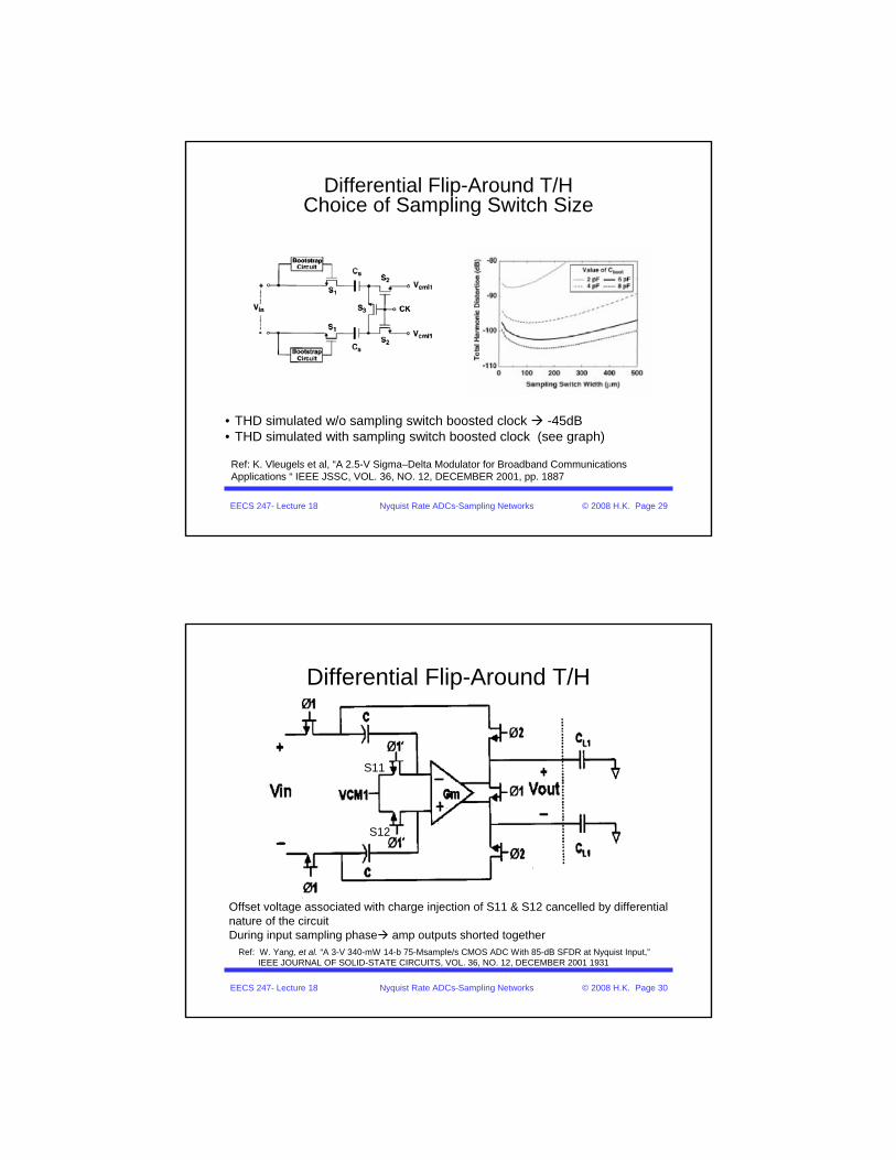
Differential Flip-Around T/HChoice of Sampling Switch Size
Ref: K. Vleugels et al, “A 2.5-V Sigma–Delta Modulator for Broadband Communications Applications “ IEEE JSSC, VOL. 36, NO. 12, DECEMBER 2001, pp. 1887
• THD simulated w/o sampling switch boosted clock -45dB• THD simulated with sampling switch boosted clock (see graph)
EECS 247- Lecture 18 Nyquist Rate ADCs-Sampling Networks © 2008 H.K. Page 30
Differential Flip-Around T/H
Ref: W. Yang, et al. “A 3-V 340-mW 14-b 75-Msample/s CMOS ADC With 85-dB SFDR at Nyquist Input,”IEEE JOURNAL OF SOLID-STATE CIRCUITS, VOL. 36, NO. 12, DECEMBER 2001 1931
Offset voltage associated with charge injection of S11 & S12 cancelled by differential nature of the circuitDuring input sampling phase amp outputs shorted together
S11
S12

EECS 247- Lecture 18 Nyquist Rate ADCs-Sampling Networks © 2008 H.K. Page 31
Differential Flip-Around T/H
• Gain=1• Feedback factor=1
φ1’φ1φ2
EECS 247- Lecture 18 Nyquist Rate ADCs-Sampling Networks © 2008 H.K. Page 32
Differential Flip-Around T/HIssues: Input Common-Mode Range
• ΔVin-cm=Vout_com-Vsig_com
Amplifier needs to have large input common-mode compliance
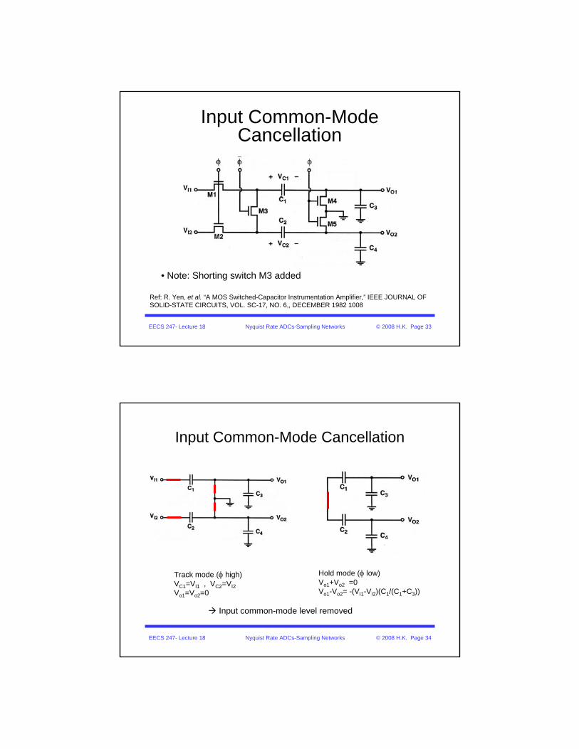
EECS 247- Lecture 18 Nyquist Rate ADCs-Sampling Networks © 2008 H.K. Page 33
Input Common-Mode Cancellation
Ref: R. Yen, et al. “A MOS Switched-Capacitor Instrumentation Amplifier,” IEEE JOURNAL OF SOLID-STATE CIRCUITS, VOL. SC-17, NO. 6,, DECEMBER 1982 1008
• Note: Shorting switch M3 added
EECS 247- Lecture 18 Nyquist Rate ADCs-Sampling Networks © 2008 H.K. Page 34
Input Common-Mode Cancellation
Track mode (φ high)VC1=VI1 , VC2=VI2Vo1=Vo2=0
Hold mode (φ low)Vo1+Vo2 =0Vo1-Vo2= -(VI1-VI2)(C1/(C1+C3))
Input common-mode level removed

EECS 247- Lecture 18 Nyquist Rate ADCs-Sampling Networks © 2008 H.K. Page 35
Switched-Capacitor Techniques Combining Track & Hold with Other Functions
• T/H + Charge Redistribution Amplifier
• T/H & Input Difference Amplifier
• T/H & Summing Amplifier
• Differential T/H Combined with Gain Stage
• Differential T/H Including Offset Cancellation
EECS 247- Lecture 18 Nyquist Rate ADCs-Sampling Networks © 2008 H.K. Page 36
T/H + Charge Redistribution Amplifier
Track mode: (S1, S3 on S2 off)VC1=Vos –VIN , VC2=0Vo=Vos

EECS 247- Lecture 18 Nyquist Rate ADCs-Sampling Networks © 2008 H.K. Page 37
T/H + Charge Redistribution AmplifierHold Mode
Hold/amplify mode (S1, S3 off S2 on)
Offset NOT cancelled, but not amplifiedInput-referred offset =(C2/C1) x VOS, & often C2<C1
2
1
2
EECS 247- Lecture 18 Nyquist Rate ADCs-Sampling Networks © 2008 H.K. Page 38
T/H & Input Difference Amplifier
Sample mode:(S1, S3 on S2 off)
VC1=Vos –VI1 , VC2=0Vo=Vos
EECS 247- Lecture 18 Nyquist Rate ADCs-Sampling Networks © 2008 H.K. Page 39
Input Difference AmplifierCont‘d
Subtract/Amplify mode (S1, S3 off S2 on)During previous phase:VC1=Vos –VI1 , VC2=0Vo=Vos
1
Offset NOT cancelled, but not amplifiedInput-referred offset =(C2/C1)xVOS, & C2<C1
EECS 247- Lecture 18 Nyquist Rate ADCs-Sampling Networks © 2008 H.K. Page 40
T/H & Summing Amplifier

EECS 247- Lecture 18 Nyquist Rate ADCs-Sampling Networks © 2008 H.K. Page 41
T/H & Summing AmplifierCont‘d
Sample mode (S1, S3, S5 on S2, S4 off)VC1=Vos –VI1 , VC2=Vos-VI3, VC3=0Vo=Vos
EECS 247- Lecture 18 Nyquist Rate ADCs-Sampling Networks © 2008 H.K. Page 42
T/H & Summing AmplifierCont‘d
Amplify mode (S1, S3, S5 off, S2, S4 on)
3

EECS 247- Lecture 18 Nyquist Rate ADCs-Sampling Networks © 2008 H.K. Page 43
Differential T/H Combined with Gain Stage
Ref: S. H. Lewis, et al., “A Pipelined 5-Msample/s 9-bit Analog-to-Digital Converter” IEEE JSSC, VOL. SC-22,NO. 6, DECEMBER 1987
Employs the previously discussed technique to eliminate the problem associated with high common-mode voltage excursion at the input of the opamp
EECS 247- Lecture 18 Nyquist Rate ADCs-Sampling Networks © 2008 H.K. Page 44
Ref: S. H. Lewis, et al., “A Pipelined 5-Msample/s 9-bit Analog-to-Digital Converter” IEEE JSSC, VOL. SC-22,NO. 6, DECEMBER 1987
Differential T/H Combined with Gain Stageφ1 High

EECS 247- Lecture 18 Nyquist Rate ADCs-Sampling Networks © 2008 H.K. Page 45
Ref: S. H. Lewis, et al., “A Pipelined 5-Msample/s 9-bit Analog-to-Digital Converter” IEEE JSSC, VOL. SC-22,NO. 6, DECEMBER 1987
• Gain=4C/C=4• Input voltage common-mode level removed opamp can have low input
common-mode compliance• Amplifier offset NOT removed
Differential T/H Combined with Gain Stage
EECS 247- Lecture 18 Nyquist Rate ADCs-Sampling Networks © 2008 H.K. Page 46
Ref: H. Ohara, et al., "A CMOS programmable self-calibrating 13-bit eight-channel data acquisition peripheral," IEEE Journal of Solid-State Circuits, vol. 22, pp. 930 - 938, December 1987.
• Operation during offset cancellation phase shown• Auxilary inputs added with Amain/Aaux.=10• During offset cancellation phase:
•Aux. amp configured in unity-gain mode: Vout=Vosmain offset stored
on CAZ & canceled
Differential T/H Including Offset Cancellation

EECS 247- Lecture 18 Nyquist Rate ADCs-Sampling Networks © 2008 H.K. Page 47
Differential T/H Including Offset CancellationOperational Amplifier
Ref: H. Ohara, et al., "A CMOS programmable self-calibrating 13-bit eight-channel data acquisition peripheral," IEEE Journal of Solid-State Circuits, vol. 22, pp. 930 - 938, December 1987.
• Operational amplifier dual input folded-cascode opamp
• M3,4 auxiliary input, M1,2 main input
• To achieve 1/10 gain ratio WM3, 4 =1/10x WM1,2 & current sources are scaled by 1/10
• M5,6,7 common-mode control
• Output stage dual cascode high DC gain
Vout=gm1,2roVin1 + gm3,4roVin2
EECS 247- Lecture 18 Nyquist Rate ADCs-Sampling Networks © 2008 H.K. Page 48
• During offset cancellation phase AZ and S1 closed main amplifier offset amplified by gm1/gm2 & stored on CAZ
• Auxiliary amp chosen to have lower gain so that:Aux. amp charge injection associated with opening of switch AZ reduced by
Aaux/Amain=1/10Insignificant increase in power dissipation resulting from addition of aux. inputs
• Requires an extra auto-zero clock phase
Differential T/H Including Offset Cancellation Phase
Voffset
+
-(VINAZ+ -VINAZ- )= -gm1,2/gm3,4Voffset

EECS 247- Lecture 18 Nyquist Rate ADCs-Sampling Networks © 2008 H.K. Page 49
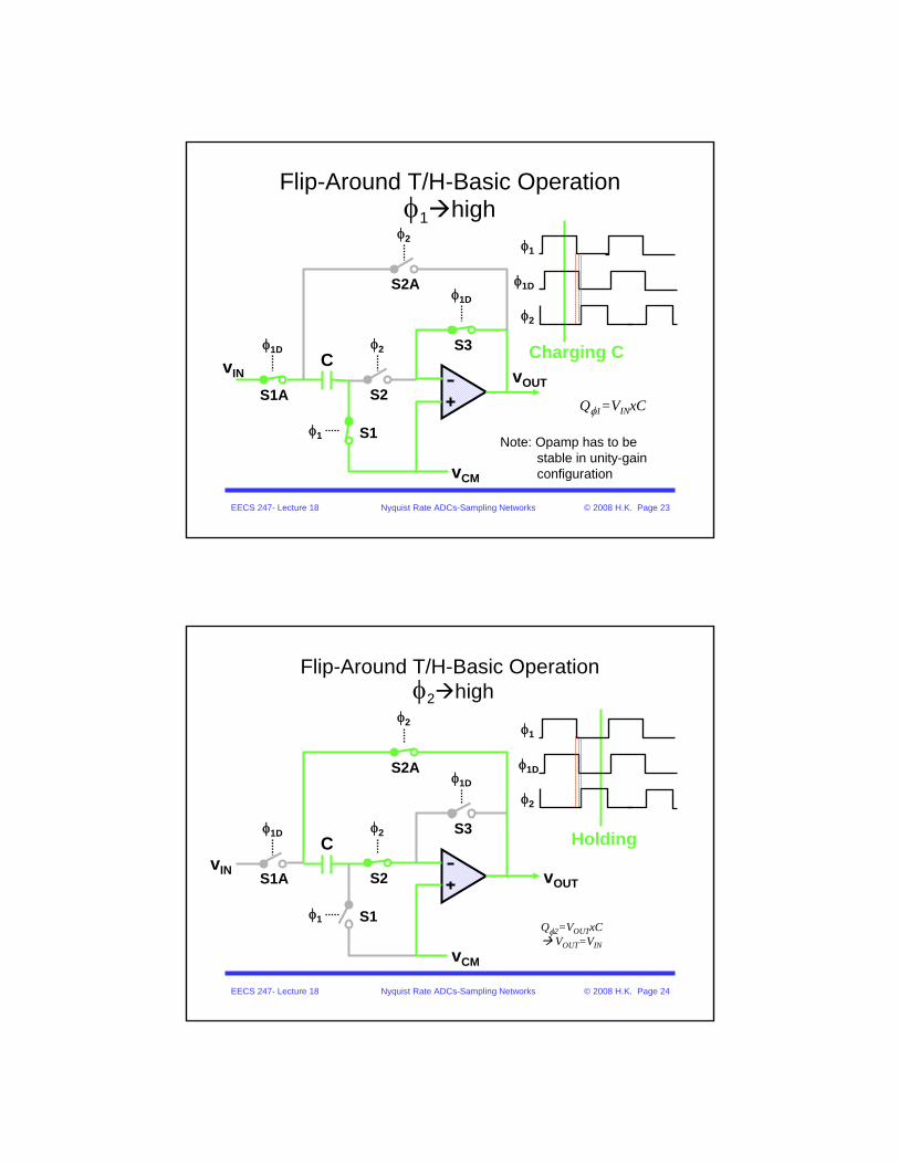
Track & HoldAperture Time Error
Time
V
Vin VOM1
VCLK
Vin
Vin +VTH
VCLK
Transition from track to hold:Occurs when device turns fully off
VCLK=Vin+VTH
Sharp fall-time wrt signal changeno aperture error
Cs
x
x
x
EECS 247- Lecture 18 Nyquist Rate ADCs-Sampling Networks © 2008 H.K. Page 50
Track & HoldAperture Time Error
Time
VSlow falling clock aperture errorVin=A sin(2π fin t)ε= fin xAx tfall /VCLK
SDR= - 20logε - 4 [dB] (imperical see Ref.)
Example: Nyquist rate 10-bit ADC & A=VCLK /4
SQNR=62dB for distortion due to aperture error
< quant noisetfall< 2x10⁻³/fin Worst case: fin= fs/2tfall < 4x10⁻³/fs
e.g. fs=100MHz, tfall<40psec
Vin
Vin +VTH
VCLK
Ref: P. J. Lim and B. A. Wooley, "A high-speed sample-and-hold technique using a Miller hold capacitance," IEEE Journal of Solid-State Circuits, vol. 26, pp. 643 - 651, April 1991.
x
x
x

EECS 247- Lecture 18 Nyquist Rate ADCs-Sampling Networks © 2008 H.K. Page 51
Track & HoldAperture Time Error
• Aperture error analysis applies to simple sampling network
• Bottom plate sampling minimizes aperture error
• Boosted clock reduces aperture error
Clock edge fall/rise trade-off between switch charge injection versus aperture error
Ref: P. J. Lim and B. A. Wooley, "A high-speed sample-and-hold technique using a Miller hold capacitance," IEEE Journal of Solid-State Circuits, vol. 26, pp. 643 - 651, April 1991.