Embed Size (px)
Citation preview

EECS 247 Lecture 16: Data Converters © 2004 H.K. Page 1
EE247Lecture 16
D/A Converters • D/A examples
– Serial charge redistribution DAC– Practical aspects of current-switch DACs– Segmented current-switch DACs
• DAC self calibration techniques– Current copiers– Dynamic element matching
ADC Converters• Sampling
– Sampling switch induced distortion– Sampling switch charge injection
EECS 247 Lecture 16: Data Converters © 2004 H.K. Page 2
Serial Charge Redistribution DAC• Nominally C1=C2
• Operation sequence:– Discharge C1 & C2, S3& S4
closed– For each bit in succession
beginning with LSB, b0:• S1 open- if bi=1 C1
precharge to VREF if bi=0 to GND
• S1 closed-S2 & S3 & S4 open- Charge sharing C1 & C2
à ½ of precharge on C1 +½ of charge previously stored on C2à C2

EECS 247 Lecture 16: Data Converters © 2004 H.K. Page 3
Serial Charge Redistribution DACExample: Input Code 101
• Example input code 101à output 5/8 VREF
• Very small area• N redistribution cycles for N-bits conversion
bo b1 b2
EECS 247 Lecture 16: Data Converters © 2004 H.K. Page 4
Resistor Ladder (MSB) & Binary Weighted
Charge Redistribution(LSB) Segmented DAC
CC2C4C8C32 C
reset
b1b2b3b5
16C
b4
Vout
b0
..........
SwitchNetwork
6bitresistorladder
6-bitbinary weighted charge redistribution DAC
• Example: 12bit DAC
– 6-bit MSB DACà R string
– 6-bit LSB DAC à binary weighted charge redistribution
• Complexity lower
than full R string– Full R stringà
4096 resistors– Segmented à
64 R + 7 Cs (65 unit caps)

EECS 247 Lecture 16: Data Converters © 2004 H.K. Page 5
Binary Weighted Charge Redistribution(MSB) &
Resistor Ladder (LSB) Segmented DAC
• Homework 6:• Compare sensitivity
of these two segmented DACs to component mismatches
CC2C4C8C32 C
VREF
reset
b1b2b3b5
16C
b4
Vout
..........
b0
SwitchNetwork
6bitresistorladder
EECS 247 Lecture 16: Data Converters © 2004 H.K. Page 6
Practical AspectsCurrent-Switched DACs
• Unit element DACs ensure monotonicity by turning on equal-weighted current sources in succession
• Typically current switching performed by differential pairs
• Based on the code only one of the diff. pair devices are onà device mismatch not an issue
• Issue: While binary weighted DAC can use the incoming binary digital code directly, unit element requiresà N to (2N-1) decoder
Binary Thermometer000 0000000001 0000001010 0000011011 0000111100 0001111101 0011111110 0111111111 1111111

EECS 247 Lecture 16: Data Converters © 2004 H.K. Page 7
SegmentedCurrent-Switched DAC
• 4-bit MSB Unit element DAC + 4-bit binary weighted DAC
• Note: 4-bit MSB DAC requires extra 4-to-16 bit decoder
• Digital code for both DACs stored in a register
EECS 247 Lecture 16: Data Converters © 2004 H.K. Page 8
Segmented Current-Switched DACCont’d
• 4-bit MSB Unit element DAC + 4-bit binary weighted DAC
• Note: 4-bit MSB DAC requires extra 4-to-16 bit decoder
• Digital code for both DACs stored in a register

EECS 247 Lecture 16: Data Converters © 2004 H.K. Page 9
Segmented Current-Switched DACCont’d
• MSB Decoderà Domino logicà Example: D4,5,6,7=1
Out=1
• Registerà Latched NAND gate:à CTRL=1 OUT=INB
Register
Domino Logic
IN
EECS 247 Lecture 16: Data Converters © 2004 H.K. Page 10
Segmented Current-Switched DACReference Current Considerations
• Iref is referenced to VDD
à Problem: Reference current varies with supply voltage

EECS 247 Lecture 16: Data Converters © 2004 H.K. Page 11
Segmented Current-Switched DACReference Current Considerations
• Iref is referenced to VssàGND
EECS 247 Lecture 16: Data Converters © 2004 H.K. Page 12
Segmented Current-Switched DACConsiderations
• Example: 2-bit MSB Unit element DAC + 3-bit binary weighted DAC
• To ensure monotonicity at the MSBà LSB transition: First OFF MSB current source is routed to LSB current generator

EECS 247 Lecture 16: Data Converters © 2004 H.K. Page 13
EECS 247 Lecture 16: Data Converters © 2004 H.K. Page 14
Current Source Replica Self-Calibration

EECS 247 Lecture 16: Data Converters © 2004 H.K. Page 15
I
I/2 I/2
Current Divider
EECS 247 Lecture 16: Data Converters © 2004 H.K. Page 16

EECS 247 Lecture 16: Data Converters © 2004 H.K. Page 17
I
I/2 I/2
Ideal Current Divider
Current Divider
I
I/2+dId /2
Real Current Divider
M1& M2 mismatched
d1 d 2d
d d1 d 2
d d
WLd
thWLd GS th
I II
2
dI I I
I I
ddI 2dV
I V V
+=
−=
= × +
−
I/2-dId /2
M1 M2M1 M2
àProblem: Device mismatch could severely limit DAC accuracy
EECS 247 Lecture 16: Data Converters © 2004 H.K. Page 18

EECS 247 Lecture 16: Data Converters © 2004 H.K. Page 19
Dynamic Element Matching
/ 2 error ∆1
I1
( )( )12
1)1(2
121)1(
1
1
1
∆−=
∆+=
o
o
II
II ( )( )12
1)2(2
121)2(
1
1
1
∆+=
∆−=
o
o
II
II
During Φ1 During Φ2
( ) ( )
2
211
2
211
)2(2
)1(2
2
o
o
I
I
III
=
∆++∆−=
+=
I2
fclk
Io
Io/2Io/2
EECS 247 Lecture 16: Data Converters © 2004 H.K. Page 20

EECS 247 Lecture 16: Data Converters © 2004 H.K. Page 21
Dynamic Element Matching
( )( )
( )( )( )214
1
2)1(
121)1(
3
121)1(
2
121)1(
1
11
1
1
1
∆+∆+=∆+=
∆−=
∆+=
o
o
o
I
II
II
II ( )( )
( )( )( )214
1
2)2(
121)2(
3
121)2(
2
121)2(
1
11
1
1
1
∆−∆−=∆−=
∆+=
∆−=
o
o
o
I
II
II
II
During Φ1 During Φ2
( )( ) ( )( )
( )21
2121
)2(3
)1(3
3
14
21111
4
2
∆∆+=
∆−∆−+∆+∆+=
+=
o
o
I
I
III
E.g. ∆1 = ∆2 = 1% à matching error is (1%)2 = 0.01%
/ 2 error ∆1
I1
I2
fclk
Io
Io/2
/ 2 error ∆2
I3 I4
fclk
Io/4Io/4
EECS 247 Lecture 16: Data Converters © 2004 H.K. Page 22
SummaryD/A Converter
• D/A architecture – Unit element – complexity proportional to 2B- excellent DNL – Binary weighted- complexity proportional to B- poor DNL– Segmented- unit element MSB + binary weighted LSBà complexity
proportional (2B1-1) + B2 – DNL compromise between the two• Static performance
– Component matching• Dynamic performance
– Glitches• DAC improvement techniques
– Symmetrical switching rather than sequential switching– Current source self calibration– Dynamic element matching

EECS 247 Lecture 16: Data Converters © 2004 H.K. Page 23
MOS Sampling Circuits
EECS 247 Lecture 16: Data Converters © 2004 H.K. Page 24
Re-Cap
• How can we build circuits that "sample"
Analog Post processing
D/AConversion
DSP
A/D Conversion
Analog Preprocessing
Analog Input
Analog Output
000...001...
110
Anti-AliasingFilter
Sampling+Quantization
"Bits to Staircase"
Reconstruction Filter

EECS 247 Lecture 16: Data Converters © 2004 H.K. Page 25
Ideal Sampling
• In an ideal world, zero resistance sampling switches would close for the briefest instant to sample a continuous voltage vIN onto the capacitor C
• Not realizable!
vIN vOUT
CS1
φ1
φ1
T=1/fS
EECS 247 Lecture 16: Data Converters © 2004 H.K. Page 26
Ideal T/H Sampling
vIN vOUT
CS1
φ1
• Vout tracks input when switch is closed• Grab exact value of Vin when switch opens• "Track and Hold" (T/H)
φ1
T=1/fS
EECS 247 Lecture 16: Data Converters © 2004 H.K. Page 27
Ideal T/H Sampling
ContinuousTime
T/H signal(SD Signal)
Clock
DT Signal
time
EECS 247 Lecture 16: Data Converters © 2004 H.K. Page 28
Practical Sampling
vIN vOUT
CM1
φ1
• kT/C noise• Finite Rswà limited bandwidth• Rsw = f(Vin) à distortion• Switch charge injection • Clock jitter

EECS 247 Lecture 16: Data Converters © 2004 H.K. Page 29
kT/C Noise
In high resolution ADCs kT/C noise usually dominates overall error (power dissipation considerations).
2
2
1212
12
−≥
∆≤
FS
B
B
B
VTkC
CTk
0.003 pF0.8 pF13 pF
206 pF52,800 pF
812141620
Cmin (VFS = 1V)B
EECS 247 Lecture 16: Data Converters © 2004 H.K. Page 30
Acquisition Bandwidth
• The resistance R of switch S1 turns the sampling network into a lowpass filter with risetime = RC = τ
• Assuming Vin is constant during the sampling period and C is initially discharged
vIN vOUT
CS1
φ1
R
( )τ/1)( tinout evtv −−=

EECS 247 Lecture 16: Data Converters © 2004 H.K. Page 31
Switch On-Resistance
Example:B = 14, C = 13pF, fs = 100MHz
T/τ >> 19.4, R << 40Ω
vIN vOUT
CS1
φ1
φ1
T=1/fS
R
( )
( )
12
12
Worst Case:
12 ln 2 1
1 12 ln 2 1
s
in outs
fin
in FS
B
Bs
V V tf
V e
V V
T
Rf C
τ
τ
−
− = << ∆
<< ∆=
<< −−
<< −−
EECS 247 Lecture 16: Data Converters © 2004 H.K. Page 32
Switch On-Resistance
( ) ( )
( )
( )( )
0
,2
for
1
DS
D triodeDSD triode ox GS TH DS ON
DS V
ON ox GS th ox DD th in
o ox DD th
inON o
DD th
dIW VI C V V V g
L dV
W Wg C V V C V V V
L L
Wg C V V
LV
g gV V
µ
µ µ
µ
→
= − − ≅
= − = − −
= −
= − −
•Switch conductance varies with input voltage•As the ratio of VDD /Vth gets smaller à conductance variation more pronounced
à Technology scaling aggravates the situation
EECS 247 Lecture 16: Data Converters © 2004 H.K. Page 33
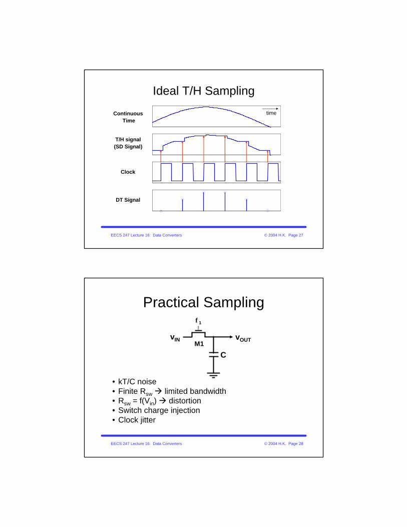
Sampling Distortion
in
DD th
outT V
12 V V
in
v
v 1 e τ
− − −
= −
10bit ADC & T/τ = 10VDD – Vth = 2V VFS = 1V
EECS 247 Lecture 16: Data Converters © 2004 H.K. Page 34
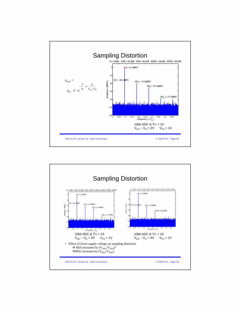
Sampling Distortion
10bit ADC & T/τ = 10VDD – Vth = 4V VFS = 1V
10bit ADC & T/τ = 10VDD – Vth = 2V VFS = 1V
• Effect of lower supply voltage on sampling distortionà HD3 increases by (VDD1/VDD2)2
àHD2 increases by (VDD1/VDD2)

EECS 247 Lecture 16: Data Converters © 2004 H.K. Page 35
Sampling Distortion
10bit ADC T/τ = 20VDD – Vth = 2V VFS = 1V
• SFDR is very sensitive to sampling distortion
• à Decreasing τ by a factor of 2 improves HD3 by 25dB!
• Solutions:• Overdesignà Larger
switchesà increased switch
charge injection• Complementary switch• Maximize VDD/VFSà decreased dynamic range
• Constant VGS ? f(Vin)à …
EECS 247 Lecture 16: Data Converters © 2004 H.K. Page 36
Complementary Switch
φ1φ1B
φ1
φ1B
gon
gop
goT =go
n + gopgo
•Complementary n & p switch advantages:•Increases the overall conductance•Linearize the switch conductance for the range Vtp< Vin <Vdd-Vtn

EECS 247 Lecture 16: Data Converters © 2004 H.K. Page 37
Complementary SwitchIssues
•Supply voltage scales down with technology scaling•Threshold voltages do not scale accordingly
Ref: A. Abo et al, “A 1.5-V, 10-bit, 14.3-MS/s CMOS Pipeline Analog-to-Digital Converter,” JSSC May 1999, pp. 599.
EECS 247 Lecture 16: Data Converters © 2004 H.K. Page 38
Complementary SwitchEffect of Supply Voltage Scaling
gon
gop
goT =go
n + gopgo
•As supply voltage scales down input voltage range for constant go shrinksà Complementary switch not effective when VDD becomes comparable to Vth
φ1φ1B
φ1
φ1B

EECS 247 Lecture 16: Data Converters © 2004 H.K. Page 39
Boosted & Constant VGS Sampling
• Increase gate overdrive voltage as much as possible + keep VGS constantØSwitch overdrive voltage is independent of signal levelØError from finite RON is linear (to first order)ØLower Ron achieved à lower time constant
VGS=const.
EECS 247 Lecture 16: Data Converters © 2004 H.K. Page 40
Constant VGS Sampling

EECS 247 Lecture 16: Data Converters © 2004 H.K. Page 41
Constant VGS Sampling Circuit
Supply
VDD = 3VVSS = 0V
Constant Vgs Switch
C11pF
C21pF
M110 / 0.35
M210 / 0.35
VDD
VP1100ns
Transient Analysisto 1.5us
M310 / 0.35
C31pF
M1210 / 0.35
M510 / 0.35
M410 / 0.35
M810 / 0.35
10 / 0.35
M9
10 / 0.35
M610 / 0.35
M11
10 / 0.35
M11
10 / 0.3510 / 0.35
M11
10 / 0.35
VS11.5V1MHz
Chold1pF
P
P
EECS 247 Lecture 16: Data Converters © 2004 H.K. Page 42
Clock Voltage DoublerSupply
VDD = 3VVSS = 0V
Clock Booster
C11pF
C21pF
M110 / 0.35
M210 / 0.35
VDD
VP1100ns
P
P_N
P_Boost
Transient Analysisto 500ns
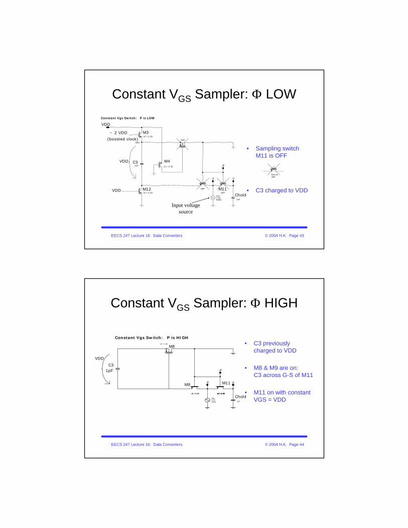
EECS 247 Lecture 16: Data Converters © 2004 H.K. Page 43
Constant VGS Sampler: Φ LOW
• Sampling switch M11 is OFF
• C3 charged to VDD
Input voltagesource
Constant Vgs Switch: P is LOW
VDD
M310 / 0.35
C31pF
M1210 / 0.35
M410 / 0.35
OFF
VS11.5V1MHz
Chold1pF
~ 2 VDD
(boosted clock)VDD
VDD
VDD
OFF M11OFF
DeviceOFF
EECS 247 Lecture 16: Data Converters © 2004 H.K. Page 44
Constant VGS Sampler: Φ HIGH
• C3 previously charged to VDD
• M8 & M9 are on:C3 across G-S of M11
• M11 on with constant VGS = VDD
Constant Vgs Switch: P is HIGH
C31pF
M810 / 0.35
10 / 0.35
M9
10 / 0.35 10 / 0.3510 / 0.3510 / 0.35
M11
10 / 0.35
VS11.5V1MHz
Chold1pF
VDD

EECS 247 Lecture 16: Data Converters © 2004 H.K. Page 45
Constant VGS Sampling
EECS 247 Lecture 16: Data Converters © 2004 H.K. Page 46
Complete Circuit
Ref: A. Abo et al, “A 1.5-V, 10-bit, 14.3-MS/s CMOS Pipeline Analog-to-Digital Converter,” JSSC May 1999, pp. 599.
Clock Multiplierfor M3
Switch
M7 & M13 for reliability

EECS 247 Lecture 16: Data Converters © 2004 H.K. Page 47
Advanced Clock Boosting
• An attempt to cancel body effect
[H. Pan et al., "A 3.3-V 12-b 50-MS/s A/D converter in 0.6um CMOS with over 80-dB SFDR," IEEE J. Solid-State Circuits, pp. 1769-1780, Dec. 2000]
EECS 247 Lecture 16: Data Converters © 2004 H.K. Page 48
Advanced Clock Boosting
• Gate tracks average of input and output, reduces effect of I·R drop at high frequencies
• Bulk also tracks signal ⇒ reduced body effect• SFDR = 76.5dB at fin=200MHz (measured)
[M. Waltari et al., "A self-calibrated pipeline ADC with 200MHz IF-sampling frontend," ISSCC 2002, Dig. Techn. Papers, pp. 314.]

EECS 247 Lecture 16: Data Converters © 2004 H.K. Page 49
Practical Sampling
vIN vOUT
CM1
φ1
• Rsw = f(Vin) à distortion• Switch charge injection
EECS 247 Lecture 16: Data Converters © 2004 H.K. Page 50
Sampling Switch Charge Injection
VIN VO
Cs
M1
VG
• First assume VIN is a DC voltage• When switch turns off à offset voltage induced on Cs• Why?
VG
t
VH
VIN
VL
VIN -Vth
VO
VIN
toff
∆V
t

EECS 247 Lecture 16: Data Converters © 2004 H.K. Page 51
SamplingSwitch Charge Injection
• Channel à distributed RC network• Channel to substrate junction capacitance à distributed & variable• Over-lap capacitance Cov = LDxWxCox associated with GS & GD overlap
MOS xtor operating in triode regionCross section view
Distributed channel resistance & gate & junction capacitances
S
G
D
B
LD
L
Cov Cov
EECS 247 Lecture 16: Data Converters © 2004 H.K. Page 52
Switch Charge InjectionSlow Clock
• Since clock fall time >> device speed à During the period (t- to toff) current in channel discharges channel charge into source
• Only source of error à Charge transfer from Cov into Cs
VG
t
VH
VIN
VL
VIN -Vth
VO
VIN
toff
∆V
tt-

EECS 247 Lecture 16: Data Converters © 2004 H.K. Page 53
Switch Charge InjectionSlow Clock
VG
t
VH
VIN
VL
VIN -Vth
VO
VIN
toff
∆V
t
D
Cov
VG
( )
( )
( )
( )
ovi th L
ov s
ovi th L
s
o i os
ov ovos th L
s s
CV V V V
C C
CV V V
CV V 1 V
C Cwhere ; V V V
C C
ε
ε
∆ = − + −+
≈ − + −
= + +
= − = − −
t-
Cs
EECS 247 Lecture 16: Data Converters © 2004 H.K. Page 54
Switch Charge InjectionSlow Clock- Example
( )
2ov ox th
ov
s
ovos th L
s
C 0.3 fF / C 5 fF / V 0.5V
C 12 x0.3 fF /.36% 7 bit
C 1pF
CV V V 1.8mV
C
µ µ
µ µε
= = =
= − = − = − → −
= − − = −
VG
t
VH
VIN
VL
VIN +Vth
VO
VIN
toff
∆V
t
VIN VO
Cs=1pF
M1
VG 12µ/0.35µ
t-

EECS 247 Lecture 16: Data Converters © 2004 H.K. Page 55
Switch Charge InjectionFast Clock
VG
t
VH
VIN
VL
VIN +Vth
VO
VIN
toff
∆V
t
VIN VO
Cs=1pF
M1
VG
• Sudden gate voltage drop à no gate voltage to establish current in channel àchannel charge has no choice but to escape out towards S & D
EECS 247 Lecture 16: Data Converters © 2004 H.K. Page 56
Switch Charge InjectionFast Clock
( )
( ) ( ) ( )( )
( )
( ) ( )
ov cho H L
ov s s
ox H i thov DH L
ov s s
o i os
ox
s
ov ox H thos H L
s s
C 1 QV V V
C C 2 C
WC V V VC 1 L 2LV V
C C 2 C
V V 1 V
1 WC Lwhere
2 C
C 1 WC L V VV V V
C 2 C
ε
ε
∆ = − − − ×+
− −−≈ − − − ×
+
= + +
= − ×
−= − − − ×
• Assumption à channel charge divided between S & D 50% & 50%• Source of error à channel charge transfer + charge transfer from Cov into Cs
VG
t
VH
VIN
VL
VIN -Vth
VO
VIN
toff
∆V
t

EECS 247 Lecture 16: Data Converters © 2004 H.K. Page 57
Switch Charge InjectionFast Clock- Example
( ) ( )
2ov ox th DD
ox
s
ov ox H thos H L
s s
C 0.3 fF / C 5 fF / V 0.5V V 3V
WLC 12 x0.35x5 fF /1 / 2 2.1% 4.5 bit
C 1pF
C 1 WC L V VV V V 9mV 26.3mV 45.3mV
C 2 C
µ µ
µ µε
= = = =
= − = = − → −
−= − − − × = − − = −
VIN VO
Cs=1pF
M1
VG 12µ/0.35µ VG
t
VH
VIN
VL
VIN -Vth
VO
VIN
toff
∆V
t
EECS 247 Lecture 16: Data Converters © 2004 H.K. Page 58
Switch Charge Injection
à Both errors are a function of clock fall time, input voltage level, source impedance & sampling capacitance
Clock fall time
ε VOS
Clock fall time
2.1%
.36%
45mV
1.8mV

EECS 247 Lecture 16: Data Converters © 2004 H.K. Page 59
Switch Charge InjectionError Reduction
( )
( )
( )( )
sON s
ox GS th
cho
s
ox H i thso
sox GS th
2
CR C W
C V VL
1 QV
2 C
WC L V V VC 1FOM V W 2 CC V V
L
LFOM
µ
µ
µ
τ
τ
= =−
∆ = −
− −= ∆ ≈ ×
−
≈
× ×
• How do we reduce the error?àReduce size switch?
àReducing switch size increases τ à increased distortionà not a viable solutionàSmall τ and ∆V à use minimum chanel lengthàFor a given technology t x ∆V àconts.
EECS 247 Lecture 16: Data Converters © 2004 H.K. Page 60
Sampling Switch Charge InjectionSummary
• Extra charge injected onto sampling capacitor @ switch device turn-off– Charge sharing with Cov
– Channel charge
• Issues:– DC offset– Input dependant error voltage à distortion
• Solutions:– Complementary switch?– Addition of dummy switches?– Bottom-plate sampling?