Embed Size (px)
Citation preview

Sam PalermoAnalog & Mixed-Signal Center
Texas A&M University
ECEN620: Network TheoryBroadband Circuit Design
Fall 2014
Lecture 13: Frequency Synthesizer Examples

Agenda
• Frequency Synthesizer Examples• Design of Frequency Synthesizers for Short Range
Wireless Transceivers• A Multi-Standard Frequency Synthesizer
2

Design of Frequency Synthesizers for Short Range
Wireless Transceivers
Ari Y. Valero - López
Department of Electrical EngineeringAnalog & Mixed-Signal Center
Texas A&M UniversityFebruary 23th, 2004A M S C
3

Most Popular Wireless Standards
ShortRange
Wireless
Bluetooth(2.45GHz, 1Mbps,10m)
WirelessLAN 802.1111a (5.25GHz, 54Mbps, 50m)11b (2.45GHz, 11Mbps, 100m)11g (2.45GHz, 24Mbps, 100m)
UWB(3.1-10.9GHz, 110Mbps, 10m)
4
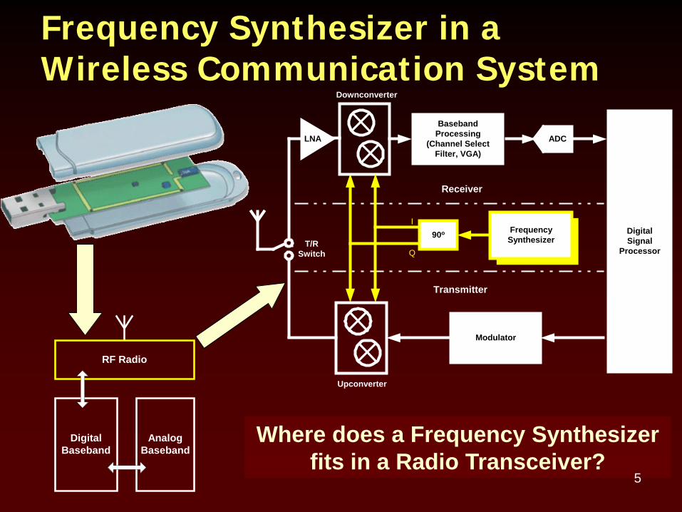
Frequency Synthesizer in a Wireless Communication System
RF Radio
DigitalBaseband
AnalogBaseband
Where does a Frequency Synthesizer fits in a Radio Transceiver?
DigitalSignal
Processor
FrequencySynthesizer
ADCLNA
90o
BasebandProcessing
(Channel SelectFilter, VGA)
Receiver
Modulator
Transmitter
Downconverter
Upconverter
T/RSwitch
I
Q
5

Function of a Frequency Synthesizer in a Radio
The Frequency Synthesizer generates the
required frequency reference for selection of a communication channel
The desired channel is downconverted to a
frequency corresponding to: fIF = fRF - fLO
DesiredChannel
Rec
eive
d Si
gnal
Syn.
Out
put
Rec
eive
r O
utpu
t
Desired Tone
fRF
fLO
fIF6
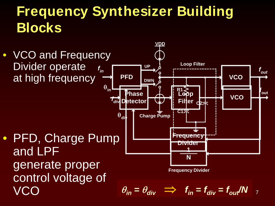
Frequency Synthesizer Building Blocks
• VCO and FrequencyDivider operateat high frequency
• PFD, Charge Pump and LPFgenerate proper control voltage of VCO
PFDfin fout
VCO
1N
C1
R1
C2
Charge Pump
Loop Filter
fdiv
VDD
UP
DWN
Frequency Divider
θin
θdiv
PhaseDetector
FrequencyDivider
foutLoopFilter VCO
θin = θdiv ⇒ fin = fdiv = fout/N 7

FS for Bluetooth Receiver
PLL
LNA
I
Q
RF filterPolyphase
Filter
Demodulator
OffsetCancellation
/Decision
2.4GHz 2MHz
Bluetooth Low IF Receiver in 0.35µm CMOS
PFD ChargePump
FrequencyDivider
fREF fOUT
Modulus Selection
LPF VCO
8

Micrograph
• Results– Tuning Range: 2.388 - 2.550 GHz– PN: -120dBc / Hz @ 1MHz– Frequency Step 1MHz– Power: 12 mA
Phase Noise Measurement
9

Dual Mode Receiver
reset
VGAwith offset cancellation
BT: 0/24dB, 1 stageWi-Fi: 0-62dB, 3 stage
Measuresignallevel
Gaincontrol
BT
Wi-Fi
BT
Wi-Fi
LPFBT: BW=600kHzWi-Fi: BW=6MHz ADC
BT: 11-bit 11MHzWi-Fi: 8-bit 44MHz
reset
Pipeline
Dig
ital M
UX
Pipeline
fref = 2MHz4.9GHz
2
2.45GHzI Q
LPF CP PFD
VCO
Phase SwitchingBlock
ProgrammableDivider
15/16 Prescaler
LNA
-15dB Attenuator
RF IN
Pipeline
Dig
ital M
UX
Pipeline
Direct Conversion Bluetooth/Wi-Fi Receiver10

Frequency Synthesizer Specifications
±60 kHz±75 kHzCenter frequency accuracy
-125 dBc/Hz @ 25 MHz
-124 dBc/Hz @ 3 MHz
Phase Noise
224 µs220 µsSettling time (max)
5 MHz1 MHzChannel Spacing
2401 – 2480 GHz
2401 – 2480 GHz
Frequency Range
IEEE 802.11bBluetooth
• Bluetooth specifications are more stringent• Complying with Bluetooth specs covers WiFi
11

Frequency Synthesizer Architecture• An Integer N Frequency Synthesizer
architecture is used.• The VCO oscillates at 5 GHz to
accommodate all the standards (requires 10% tuning range).
• A Divide-by-2 generates quadrature outputs for BT and 802.11b.
fref = 2MHz 4.9GHz
2
2.45GHz IQ
PFD CP LPF
VCO
Phase SwitchingBlock
ProgrammableDivider
15/16 Prescaler
BluetoohIEEE 802.11b
12

Design Considerations
( )( )
>−
+−∆
−−
<
−
∆
=
1 12
1ln
11
1 1
ln
2
2
2
2
ζξε
ξξ
ωξξ
ζωζε
ref
n
n
ref
lock
Nf
ζ
Nf
t
+
−
+=
−
=
−−
−−
1
1tan1tan
tantan
2
1
1
2
11
2
121
CCC
Cm
p
z
z
pm
φ
ωω
ωω
φ
• Phase Margin
• Settling Time
20 30 40 50 60 70 800
0.2
0.4
0.6
0.8
1
1.2
1.4
Phase Margin [Degrees]
Damping Factorξωn/ωc
20 30 40 50 60 70 801.15
1.2
1.25
1.3
1.35
1.4
1.45
1.5
1.55
1.6
Phase Margin [Degrees]
ω-3dB/ωc
( ) ( ) 11212 2223 ++++=− ζζωω ndB
• Design Parameters– Loop Bandwidth– VCO Gain– Charge Pump Current– Loop Filter Components
( )( )m
mvcofpd
NKKK
φφτζ
cos2sin
2==
13

Loop Filter
C1
R1
C2Vo
Icp
+
-
Kvco = 300MHz/V C1 = 340 pF
Icp = 35 µA C2 = 26.15 pF
N = 2450 R1 = 52.6 kΩ
• Trade offs– Settling Time– Close-in Phase Noise– Total Capacitance– Charge Pump Current
Loop Bandwidth = 35 kHz Phase Margin = 60°14

Capacitance Multiplier
• SchematicVdd
C
5 µA
VbiasN
VbiasPIin
1:M
1:M
M1
M2
M4
M3
A
B
10
+=
Mzzin
Z0i1 Mi1
iin
Zin
• Model
15

Loop Filter Layout• Active Filter.
• Reduced area• 240µm x 280µm
• Passive Filter. • Reduced spurs• 430µm x 780µm
Active vs. Passive 16

Phase Switching Prescaler
• Architecture
Phase switching prescaler for reduced power consumption
compared with traditional architectures.
Total Current: 4 mA
fin /4fin
÷ 2IQIQ
f in /2
5GHz
2.5GHz 1.25
GHz
To Mixers LO Port
625MHz
÷ 2IQIQ
PhaseSelection
÷ 2
ModulusControl
÷ 2fout
IQIQ
÷ 2
PhaseSelection
fin /8
/2 /
2
/2
/2
/2
I
QI
Q
p0p2p4p6
p1p3p5p7
ModulusControl
Mux
15/16 Dual Modulus 17

Phase Switching Prescaler
1 2 3 4 5 6 7 1 2 3 4 5 6 7 8
1 2 3 4 1 2 3 4
1 2 3
fout
Mux
p7
p6
p5
• Circuit Operation
fin /4
1.25GHz 625
MHz
IQIQ
PhaseSelection
÷ 2
ModulusControl
÷ 2fout
IQIQ
÷ 2
PhaseSelection
fin /8
/2
/2
p0p2p4p6
p1p3p5p7
ModulusControl
Mux
18

Phase Switching Prescaler
Vdd
CLK CLK
D
Q
Q
Vbias
R R
D
Ibias
÷ 2IQIQ
D Q
Q
D Q
QCLK
I Q
1st stage 2nd stage 3rd stage Ibias 500 µA 375 µA 250 µAR 1 kΩ 1.3 kΩ 2 kΩ
• Implementation: High Frequency D Flip-flop
2
2.45GHz IQ
Phase SwitchingBlock
15/16 Prescaler
19

Measurement Results• Phase Noise
Phase Noise:-124 dBc/Hz @ 3MHz
Settling time :150 µs (220 µs spec)
• Settling Time
20

Measurement Results
• Output Spectrum
Worst case measurement
Phase error ≈ 3°
Magnitude error ≈ 1dB
Tuning Range:
2.391 – 2.498 GHz
• I/Q Mismatch
21

Summary of FS Testing Results
Parameter Value Units
Frequency Range 2400 - 2500 GHz
Phase Noise -124 dBc @ 3MHz
Settling Time 150 µs
Reference Spur -35 dBc
Power Consumption 31.25 mW
I/Q MismatchPhaseAmplitude
< 3< 1
°dB 22

Summary of Testing Results• Power Consumption Distribution
VCO3mA
5GHz Buffer1.5mA
2.4 GHz Buffers3mA
Prescaler4mA
Digital0.6mA
CP, CM, Bias0.4mA
Total current consumption = 12.5mAwith buffers
23
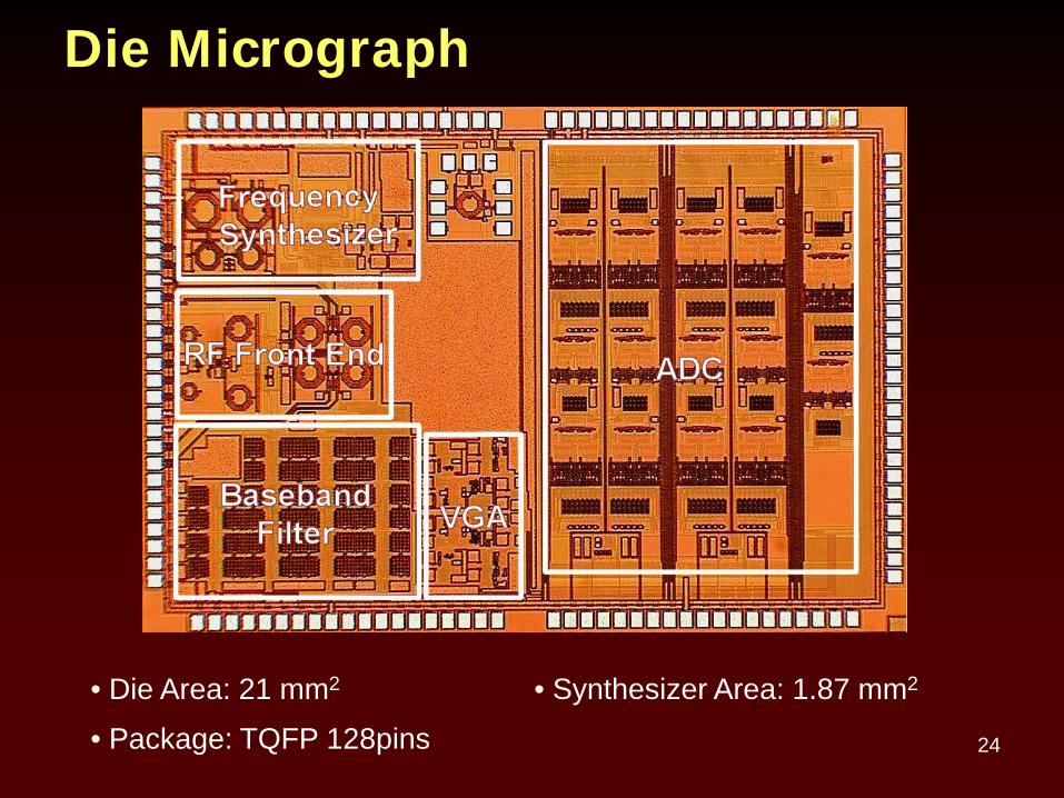
Die Micrograph
• Die Area: 21 mm2
• Package: TQFP 128pins
• Synthesizer Area: 1.87 mm2
24

A Multi-standard Frequency Synthesizer
Sung Tae MoonApril 4, 2003
25

Bluetooth + WLAN 802.11b Specification
Bluetooth WLAN 802.11b• Band 2.4~2.48 2.4~2.472 GHz• Channel 1 MHz 5 MHz• Settling 239 µsMAX 220 µsMAX
• Phase noise −124 dBc −126 dBc@3 MHz @25 MHz
• Accuracy ±75 kHz ±60 kHz
26
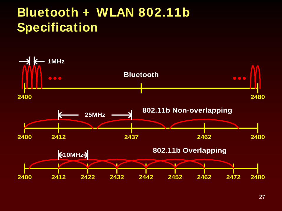
Bluetooth + WLAN 802.11b Specification
2400 2480
25MHz
2400 24802412 2437 2462
2400 24802412 2422 2432 2442 2452 2462 2472
Bluetooth
802.11b Non-overlapping
802.11b Overlapping
1MHz
10MHz
27

What’s the Challenge?
• Limited loop bandwidth : 100 kHz– Results in slow settling– Adaptive dual-loop PLL
• Wide band VCO Necessary– Multi-frequency bands to allow for low KVCO
and wide tuning range– Automatic calibration to switch between bands
28

Adaptive Dual-loop PLL
PFD1 CP1 LoopFilterfREF
%N
IL
VCO
PFD2 CP2
Dead-zone IH
Auxiliary Loop
29

Adaptive Dual-loop PLL
• Less costly solution to limited loop-bandwidth problem
• Flexible Loop-bandwidth• Glitch problem between bandwidth
switching• Smooth transition using dead-zone• Improved dead-zone control
30

Dead-zone Control
PFD1 CP1 LoopFilter
PFD2 CP2
Dead-zone
fREF
%N
IL
IH VCO
Digital Control
31

MATLAB simulation
32

Wide-Band VCO with Calibration
Vc
VcD0D1
• Discrete capacitor array– Without array, tuning gain is
too high• With array, both wide band
operation and low tuning gain are achieved
• Comparator loop for automatic calibration
33

Automatic Calibration
PLL VCO
Comparator
HI LO
34
Next Time
• Fractional-N Frequency Synthesizers
35


![ECEN620: Network Theory Broadband Circuit Design Fall 2019ece.tamu.edu/~spalermo/ecen620/lecture07_ee620_vcos.pdf• VCO Jitter 23. Oscillator Noise 24 Jitter [McNeill] Phase Noise](https://img.dokumen.tips/doc/110x75/5eb0f0afdb23476d411ded00/ecen620-network-theory-broadband-circuit-design-fall-spalermoecen620lecture07ee620vcospdf.jpg)