Embed Size (px)
Citation preview
Sam Palermo Analog & Mixed-Signal Center
Texas A&M University
ECEN620: Network Theory Broadband Circuit Design
Fall 2012
Lecture 22: Limiting Amplifiers (LAs)
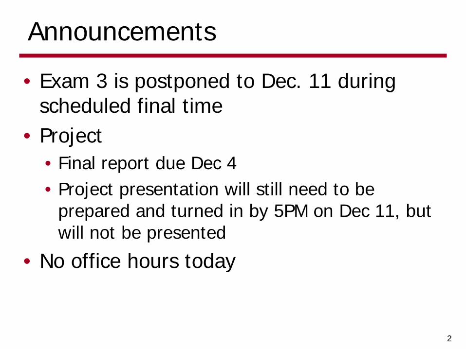
Announcements
• Exam 3 is postponed to Dec. 11 during scheduled final time
• Project • Final report due Dec 4 • Project presentation will still need to be
prepared and turned in by 5PM on Dec 11, but will not be presented
• No office hours today
2
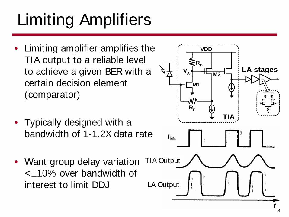
Limiting Amplifiers
• Limiting amplifier amplifies the TIA output to a reliable level to achieve a given BER with a certain decision element (comparator)
• Typically designed with a bandwidth of 1-1.2X data rate
• Want group delay variation <±10% over bandwidth of interest to limit DDJ
3
RF
M1
M2
RD
VDD
VA
TIA
LA stages
TIA Output
LA Output
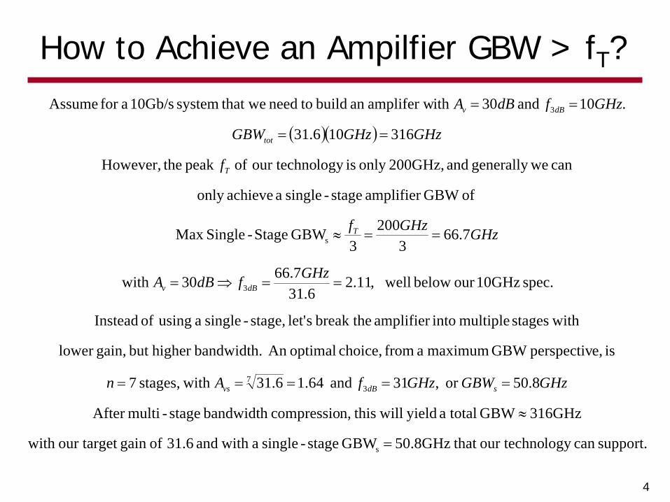
How to Achieve an Ampilfier GBW > fT?
4
( )( )
support.can logy our techno that 50.8GHzGBW stage-single a with and 31.6 ofgain our targetwith
316GHzGBW totala yield will thisn,compressiobandwidth stage-multiAfter
8.50or ,31 and 64.16.31 with stages, 7
is e,perspectivGBW maximum a from choice, optimalAn bandwidth.higher but gain,lower
withstages multiple intoamplifier break the slet' stage,-single a using of Instead
spec. 10GHzour below well,11.26.31
7.6630with
7.663
2003
GBW Stage-SingleMax
ofGBW amplifier stage-single a achieveonly
can wegenerally and 200GHz,only islogy our techno of peak theHowever,
316106.31
.10 and 30ith amplifer wan build toneed that wesystem 10Gb/s afor Assume
s
37
3
s
3
=
≈
=====
==⇒=
==≈
==
==
GHzGBWGHzfAn
GHzfdBA
GHzGHzf
f
GHzGHzGBW
GHzfdBA
sdBvs
dBv
T
T
tot
dBv
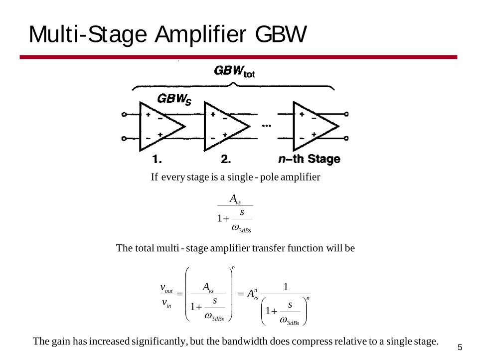
Multi-Stage Amplifier GBW
5 stage. single a torelative compress doesbandwidth but the tly,significan increased hasgain The
1
1
1
be illfunction wtransfer amplifier stage-multi totalThe
1
amplifier pole-single a is stageevery If
33
3
n
dBs
nvs
n
dBs
vs
in
out
dBs
vs
sAs
Avv
sA
+
=
+=
+
ωω
ω
Multi-Stage Amplifier Bandwidth Compression
6 approach.amplifier stage-multi a with achieved becan GBW in increaset significan a Thus,
gain.in increase than therateslower much aat although compress, doesbandwidth stage-multi totalThe
12
21
21
21
whereis , bandwidth, dB-3amplifier totalThe
1
33
2
3
3
2
3
3
3
3
3
−=
=
+
=
+
=+
=
ndBsdBtot
n
dBs
dBtot
nvs
n
dBs
dBtot
vs
n
n
dBs
dBtotin
out
dBtot
AA
AjA
vv
ωω
ωω
ωω
ωω
ω
Optimum Number of Gain Stages
7
12
stagesn with gain totala achieve will weand
1212
isbandwidth total that theRecall
bandwidth.gain potentail maximum afor stages ofnumber
optimuman bemust thereThus, stages. cascaded with compress willbandwidth theHowever, stages.
ofnumber theincrease andgain stage-per thereduce tohave webandwidth,high a achieve toneed weIf
rad/s)in isGBW here (Note,
supportcan y technolog that the stage-per maximum a is e that therAssuming
1
13
1
11
33
33
−=⇒=
−=−=
=⇒=
n
ntot
sdBtot
ntotvs
tot
n
vs
sndBsdBtot
vs
sdBsdBsvss
s
GGBWGA
G
AGBW
AGBWAGBW
GBW
ω
ωω
ωω
Optimum Number of Gain Stages
8
( ) ( ) ( ) 02lnlnln1ln21
2lnln1ln
optimum. same theyield should thisas
r,denominato theof log natural theminimize slet' easier, thismake toMoreover,
02ln
1
2ln1
stages ofnumber w.r.t thereciprocal its minimize slet' ,expression thismaximizing of instead Also,
2ln112
ionapproximat following
themake slet' this,do order toIn bandwidth. themaximize tolike would wegain, lgiven tota aFor
1
3
1
3
1
3
1
1
13
=
−+=
=
=
=
=
≈−=
stotn
totsdBtot
ntot
sdBtot
ntot
sdBtot
ntot
sn
ntot
sdBtot
GBWGn
ndndG
GBWn
dnd
dnd
GGBW
ndnd
dnd
GGBW
n
nGGBW
GGBW
ω
ω
ω
ω
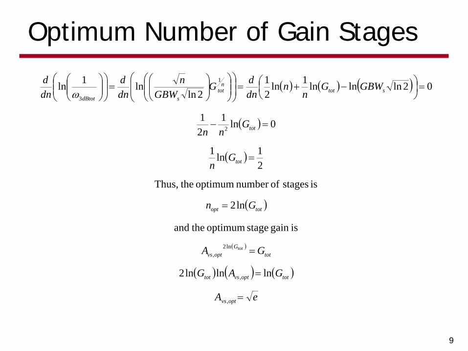
Optimum Number of Gain Stages
9
( ) ( ) ( )
( )
( )
( )
( )
( ) ( ) ( )
eA
GAG
GA
Gn
Gn
Gnn
GBWGn
ndndG
GBWn
dnd
dnd
optvs
totoptvstot
totG
optvs
totopt
tot
tot
stotn
totsdBtot
tot
=
=
=
=
=
=−
=
−+=
=
,
,
ln2,
2
1
3
lnlnln2
isgain stage optimum theand
ln2
is stages ofnumber optimum theThus,
21ln1
0ln121
02lnlnln1ln21
2lnln1ln
ω
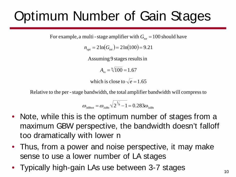
Optimum Number of Gain Stages
10
( ) ( )
dBsdBs
vs
totopt
tot
e
A
Gn
G
39
1
33dBtot
9
283.012
tocompress willbandwidth amplifier total thebandwidth, stage-per the toRelative
65.1 toclose iswhich
67.1100
in results stages 9 Assuming
21.9100ln2ln2
have should 100with amplifier stage-multi a example,For
ωωω =−=
=
==
===
=
• Note, while this is the optimum number of stages from a maximum GBW perspective, the bandwidth doesn’t falloff too dramatically with lower n
• Thus, from a power and noise perspective, it may make sense to use a lower number of LA stages
• Typically high-gain LAs use between 3-7 stages
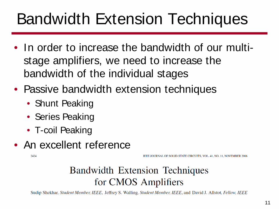
Bandwidth Extension Techniques
• In order to increase the bandwidth of our multi-stage amplifiers, we need to increase the bandwidth of the individual stages
• Passive bandwidth extension techniques • Shunt Peaking • Series Peaking • T-coil Peaking
• An excellent reference
11
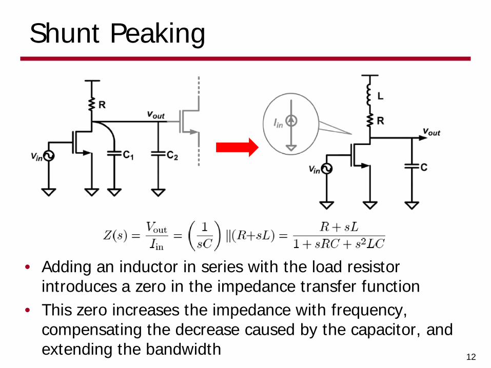
Shunt Peaking
12
• Adding an inductor in series with the load resistor introduces a zero in the impedance transfer function
• This zero increases the impedance with frequency, compensating the decrease caused by the capacitor, and extending the bandwidth

Shunt Peaking
13
• While the inductor can increase the bandwidth significantly, frequency peaking can occur if the inductor is too big
• For a flat frequency response, ~70% bandwidth increase can be achieved
• A maximum 85% bandwidth increase is possible with 1.5dB of peaking
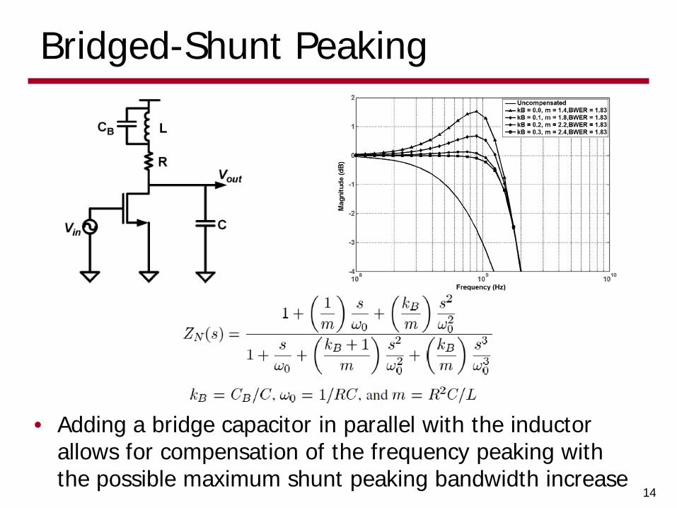
Bridged-Shunt Peaking
14
• Adding a bridge capacitor in parallel with the inductor allows for compensation of the frequency peaking with the possible maximum shunt peaking bandwidth increase
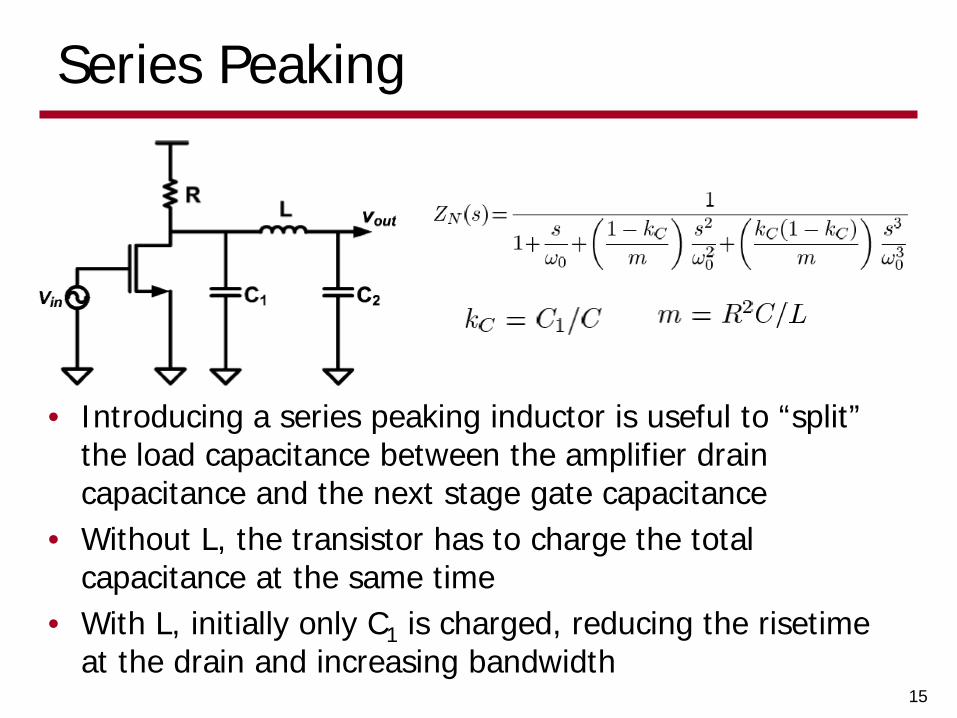
Series Peaking
• Introducing a series peaking inductor is useful to “split” the load capacitance between the amplifier drain capacitance and the next stage gate capacitance
• Without L, the transistor has to charge the total capacitance at the same time
• With L, initially only C1 is charged, reducing the risetime at the drain and increasing bandwidth
15
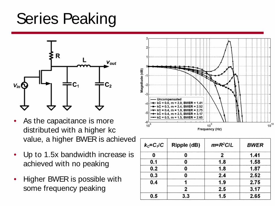
Series Peaking
• As the capacitance is more distributed with a higher kc value, a higher BWER is achieved
• Up to 1.5x bandwidth increase is achieved with no peaking
• Higher BWER is possible with some frequency peaking
16

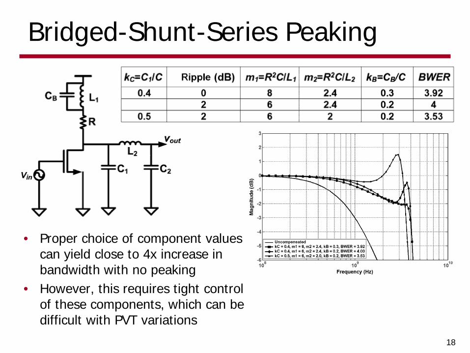
Bridged-Shunt-Series Peaking
17
• Combining both shunt and series peaking can yield even higher bandwidth extension
Bridged-Shunt-Series Peaking
18
• Proper choice of component values can yield close to 4x increase in bandwidth with no peaking
• However, this requires tight control of these components, which can be difficult with PVT variations
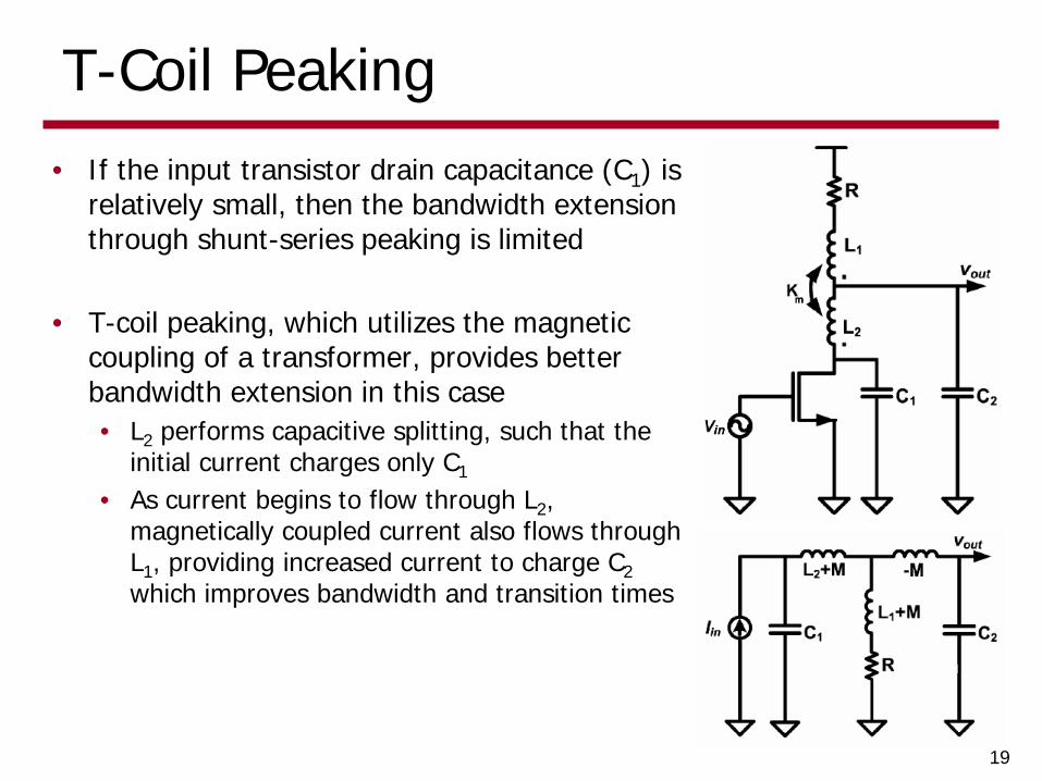
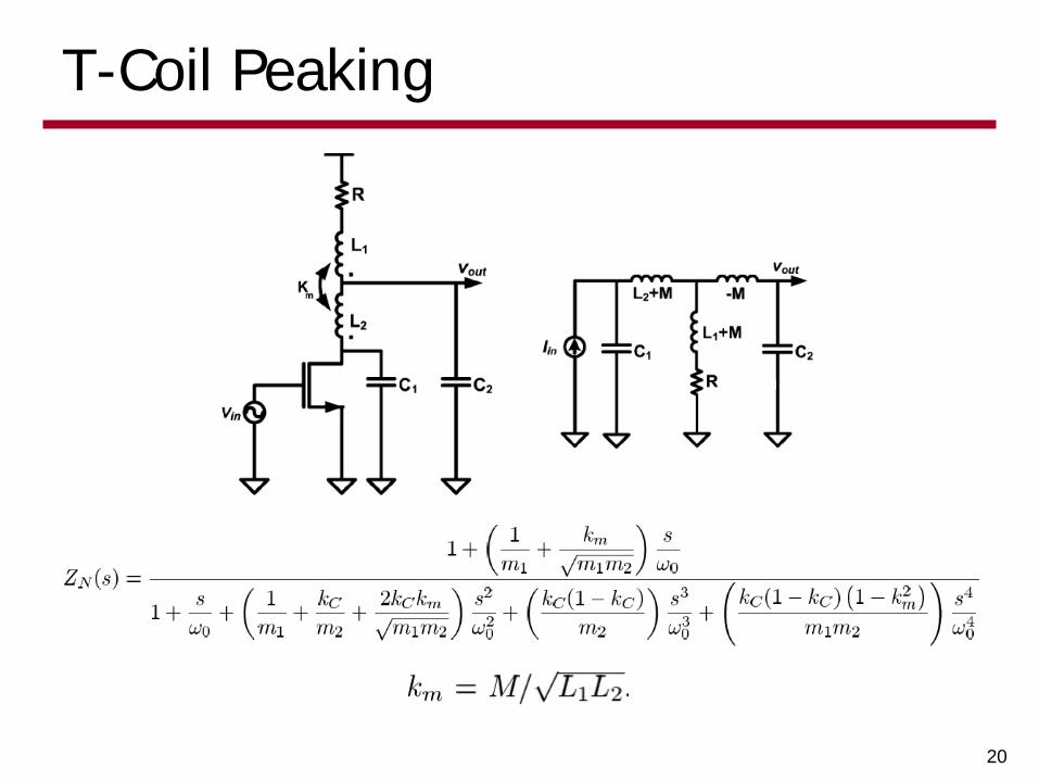
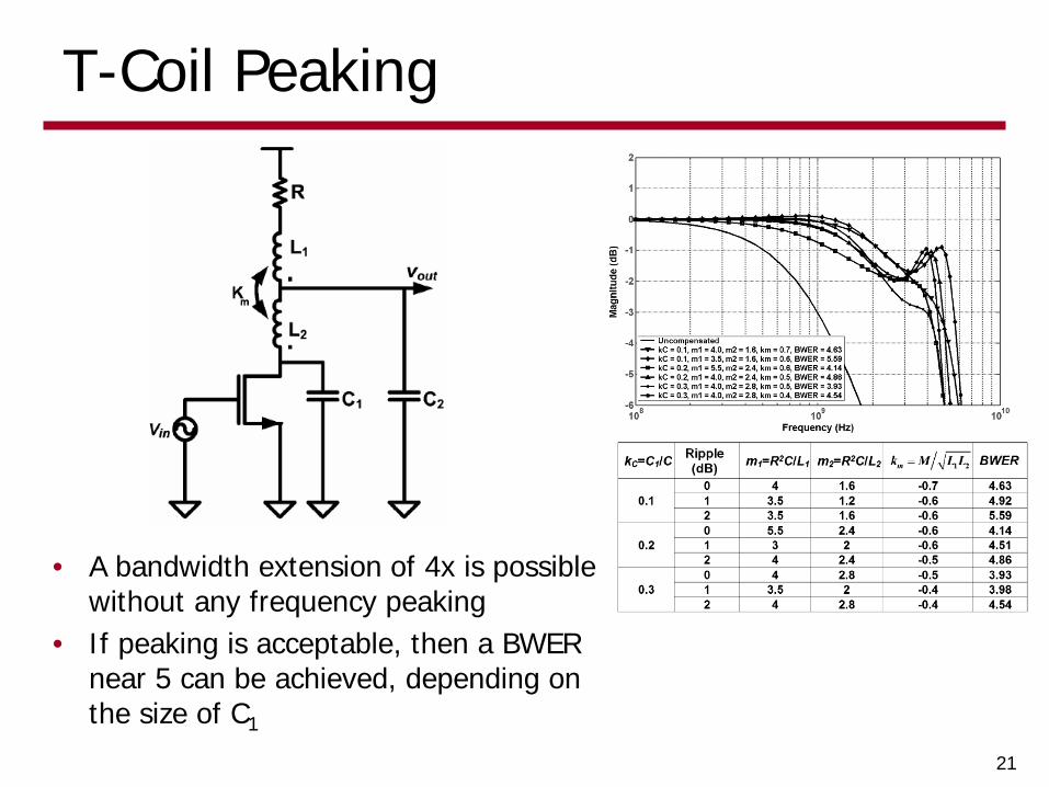
T-Coil Peaking
19
• If the input transistor drain capacitance (C1) is relatively small, then the bandwidth extension through shunt-series peaking is limited
• T-coil peaking, which utilizes the magnetic coupling of a transformer, provides better bandwidth extension in this case • L2 performs capacitive splitting, such that the
initial current charges only C1
• As current begins to flow through L2, magnetically coupled current also flows through L1, providing increased current to charge C2 which improves bandwidth and transition times
T-Coil Peaking
20
T-Coil Peaking
• A bandwidth extension of 4x is possible without any frequency peaking
• If peaking is acceptable, then a BWER near 5 can be achieved, depending on the size of C1
21
Active Bandwidth Extension Techniques
• While passive techniques offer excellent bandwidth extension at near zero power cost, there are some disadvantages • Generally large area • Process support/characterization of inductors/transformers
• Active circuit techniques can also be employed to extend amplifier bandwidth
• Some active bandwidth extension techniques • Negative Miller Capacitance • Active Negative Feedback
• There are numerous other techniques, but that is all we have time for this semester
22
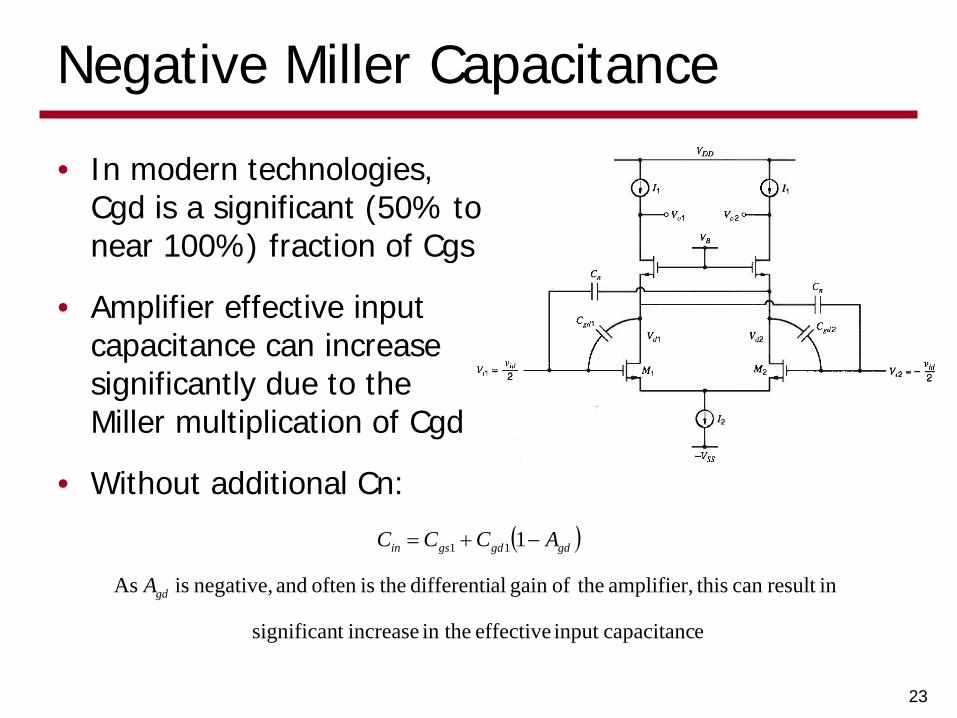
Negative Miller Capacitance
• In modern technologies, Cgd is a significant (50% to near 100%) fraction of Cgs
• Amplifier effective input capacitance can increase significantly due to the Miller multiplication of Cgd
• Without additional Cn:
23
( )
ecapacitancinput effective in the increaset significan
in result can thisamplifier, theofgain aldifferenti theisoften and negative, is As
111
gd
gdgdgsin
A
ACCC −+=
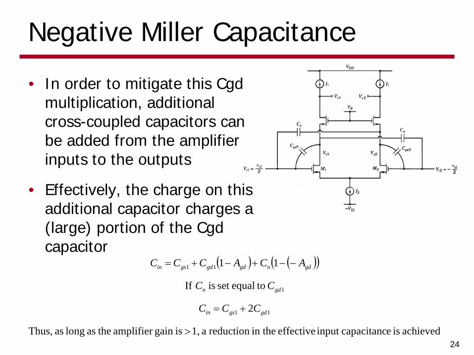
Negative Miller Capacitance
• In order to mitigate this Cgd multiplication, additional cross-coupled capacitors can be added from the amplifier inputs to the outputs
• Effectively, the charge on this additional capacitor charges a (large) portion of the Cgd capacitor
24
( ) ( )( )
achieved is ecapacitancinput effective in thereduction a 1, isgain amplifier theas long as Thus,
2
toequalset is If
11
11
1
11
>
+=
−−+−+=
gdgsin
gdn
gdngdgdgsin
CCC
CC
ACACCC
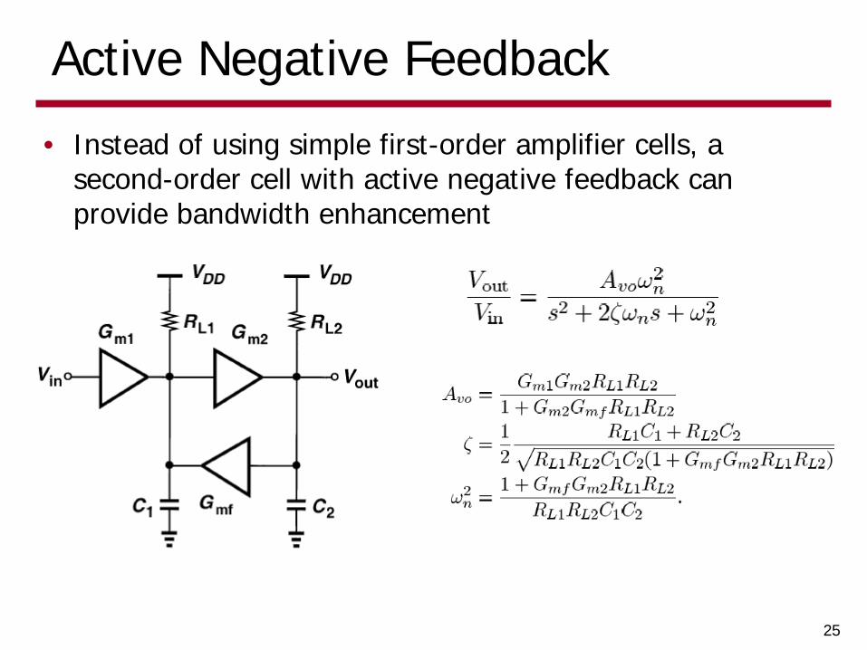
Active Negative Feedback
• Instead of using simple first-order amplifier cells, a second-order cell with active negative feedback can provide bandwidth enhancement
25
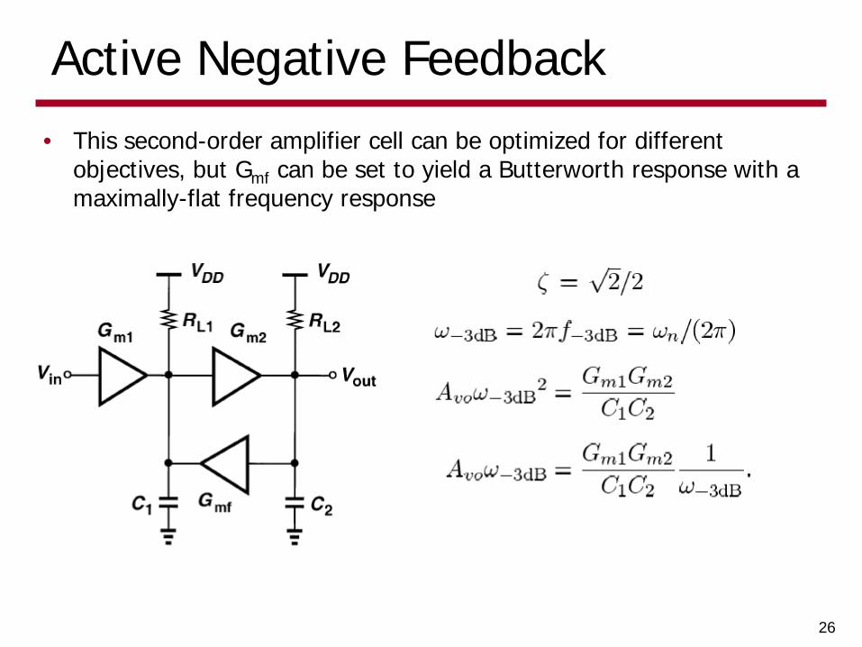
Active Negative Feedback • This second-order amplifier cell can be optimized for different
objectives, but Gmf can be set to yield a Butterworth response with a maximally-flat frequency response
26
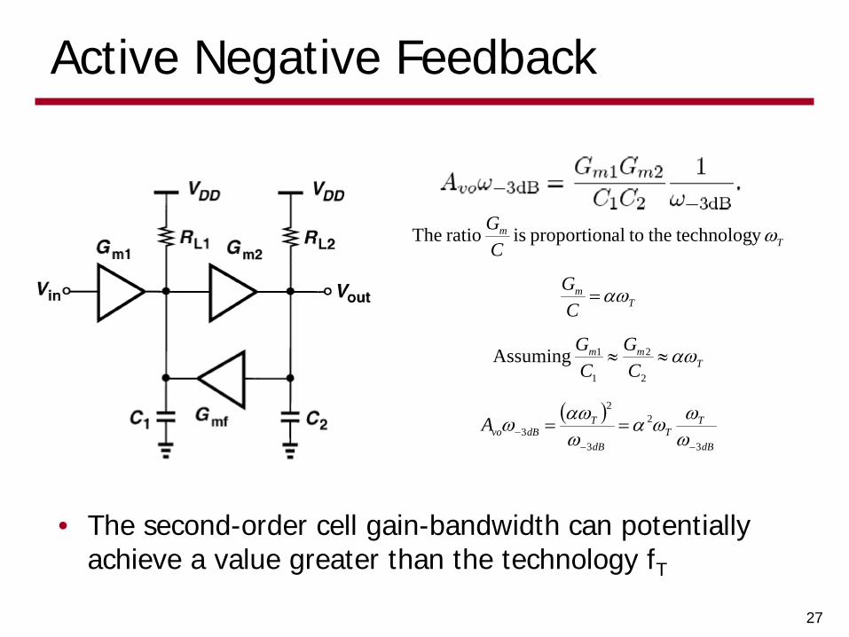
Active Negative Feedback
• The second-order cell gain-bandwidth can potentially achieve a value greater than the technology fT
27
( )dB
TT
dB
TdBvo
Tmm
Tm
Tm
A
CG
CG
CG
CG
3
2
3
2
3
2
2
1
1 Assuming
y technolog the toalproportion is ratio The
−−− ==
≈≈
=
ωωωα
ωαωω
αω
αω
ω
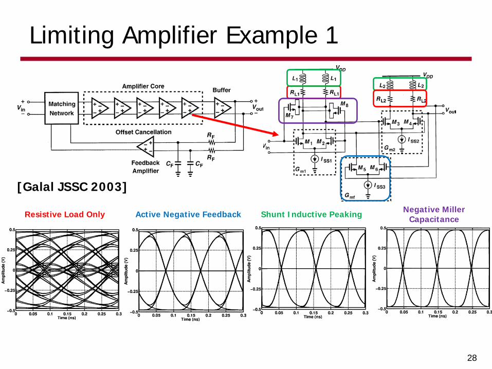
Limiting Amplifier Example 1
28
[Galal JSSC 2003]
Resistive Load Only Active Negative Feedback Shunt Inductive Peaking Negative Miller Capacitance
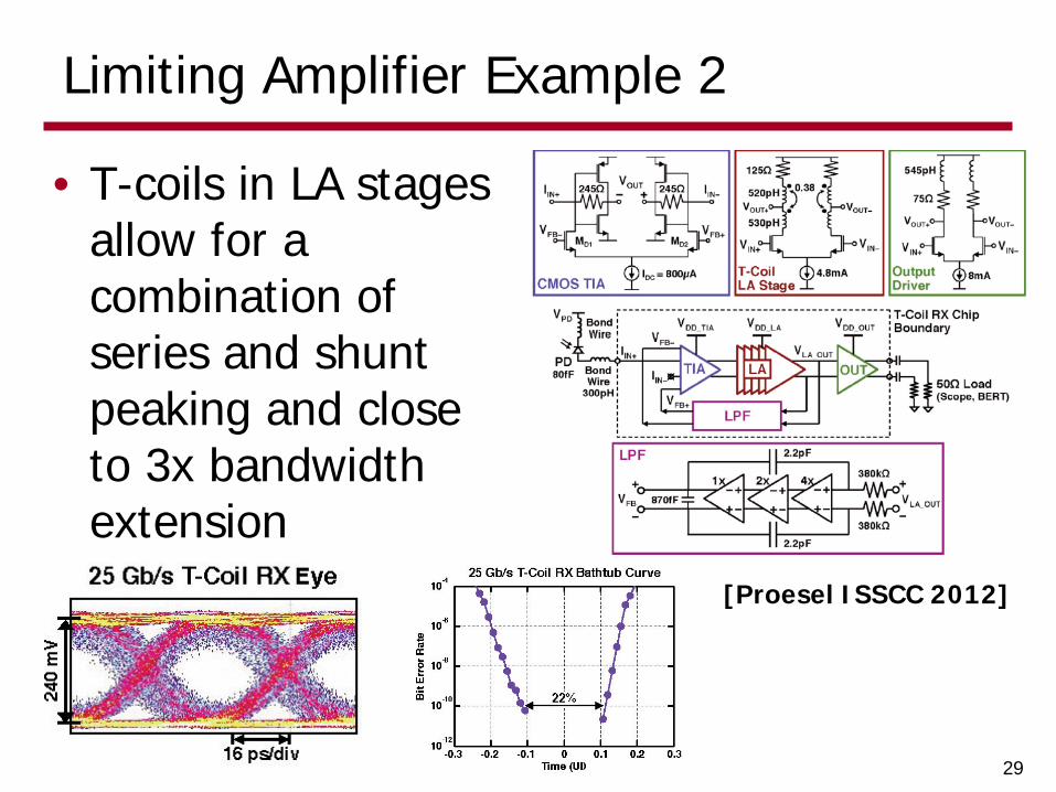
Limiting Amplifier Example 2
• T-coils in LA stages allow for a combination of series and shunt peaking and close to 3x bandwidth extension
29
[Proesel ISSCC 2012]
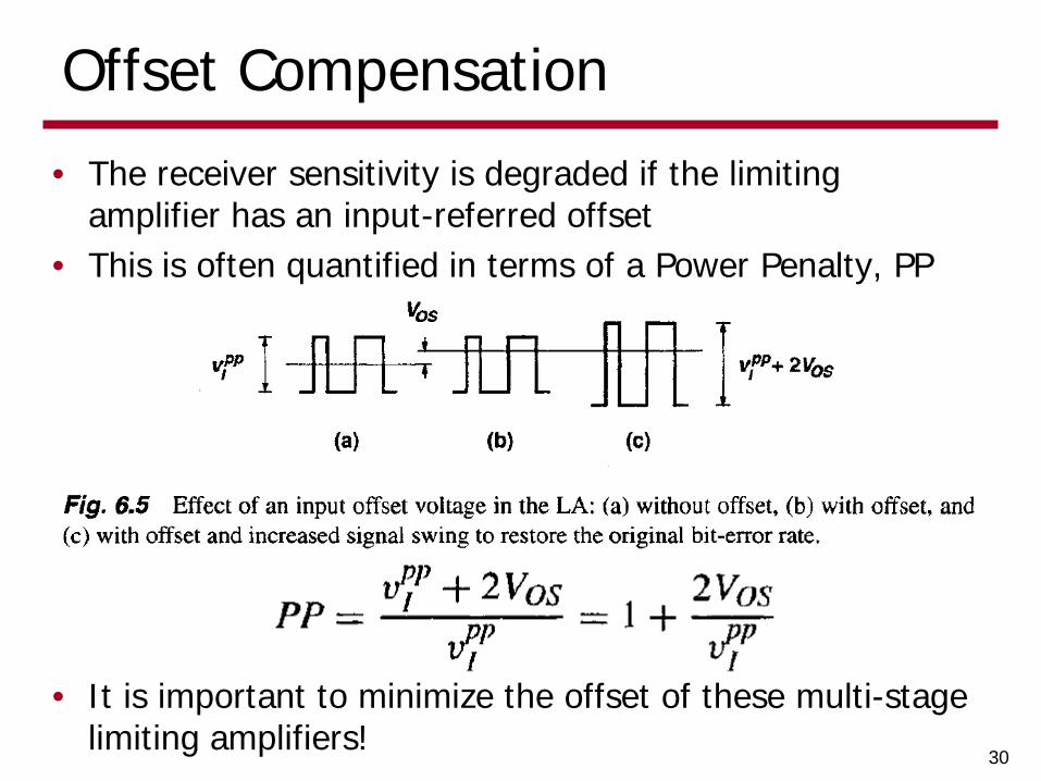
Offset Compensation
• The receiver sensitivity is degraded if the limiting amplifier has an input-referred offset
• This is often quantified in terms of a Power Penalty, PP
30
• It is important to minimize the offset of these multi-stage limiting amplifiers!
Offset Compensation
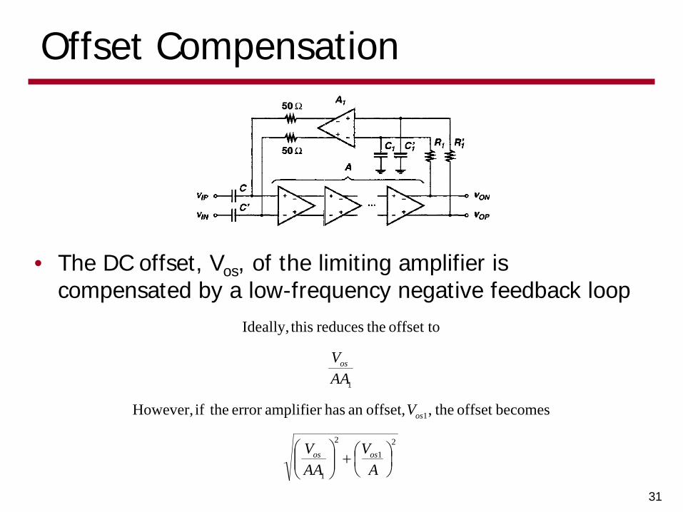
• The DC offset, Vos, of the limiting amplifier is compensated by a low-frequency negative feedback loop
31
21
2
1
1
1
becomesoffset the, offset,an hasamplifier error theif However,
offset to thereduces thisIdeally,
+
A
VAAV
V
AAV
osos
os
os
Offset Compensation
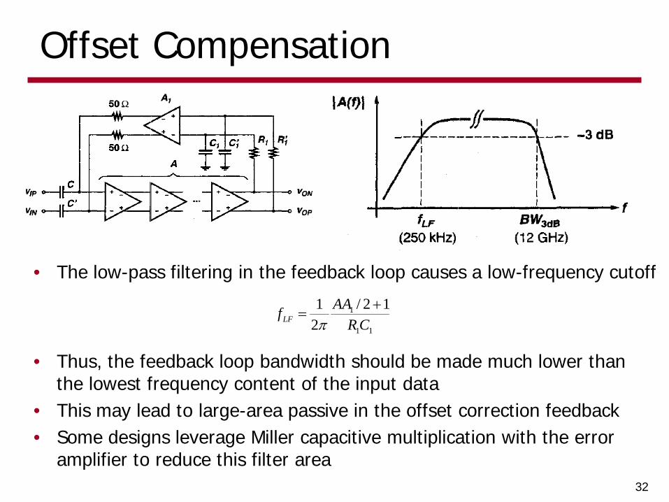
• The low-pass filtering in the feedback loop causes a low-frequency cutoff
32
11
1 12/21
CRAAfLF
+=
π
• Thus, the feedback loop bandwidth should be made much lower than the lowest frequency content of the input data
• This may lead to large-area passive in the offset correction feedback • Some designs leverage Miller capacitive multiplication with the error
amplifier to reduce this filter area


![ECEN620: Network Theory Broadband Circuit Design Fall 2014 · 2020. 10. 30. · Multiphase Clock Generation ... • Sinusoidal • Linear [Bulzacchelli] [Weinlader] 15. DLL Frequency](https://img.dokumen.tips/doc/110x75/60eb74e02337a65b583b6c1e/ecen620-network-theory-broadband-circuit-design-fall-2014-2020-10-30-multiphase.jpg)