Embed Size (px)
Citation preview

Sam PalermoAnalog & Mixed-Signal Center
Texas A&M University
ECEN 620: Network TheoryBroadband Circuit Design
Fall 2020
Lecture 16: High-Speed I/O Overview

Announcements• Exam 2 is on Nov. 19
• Covers through Lecture 15• Take home format assigned/turned-in via Google
Classroom• Posted at ~8AM and due 7PM• Open notes/references
• Project• Final report due Nov 24• Presentation on Dec 4 (2PM-4:30PM)
2
3
Outline
• Introduction
• Electrical I/O Overview Channel characteristics Transmitter & receiver circuits Clocking techniques & circuits
• Conclusion

4
ECEN 720: High-Speed Links Circuits & Systems
• Spring 2021• https://people.engr.tamu.edu/spalermo/ecen720.html• Covers system level and circuit design issues relevant to
high-speed electrical and optical links• Channel Properties
• Modeling, measurements, communication techniques
• Circuits• Drivers, receivers, equalizers, clocking
• Project• Link system design with statistical BER analysis tool• Circuit design of key interface circuits
• Prerequisite: ECEN 474/704 or my approval

High-Speed Serial I/O• Found in applications ranging from
high-end computing systems to smart mobile devices
• Typical processor platform• Processor-to-memory: DDR4• Processor-to-peripheral: PCIe & USB • Storage: SATA• Network: LAN
• Mobile systems• DSI : Display Serial Interface• CSI : Camera Serial Interface• UniPRO : MIPI Universal Protocol
5
AMD EPYC Rome Platform

6
Chip-to-Chip Signaling TrendsDecade Speeds Transceiver Features1980’s >10Mb/s Inverter out, inverter in
1990’s >100Mb/s Termination Source-synchronous clk.
2000’s >1 Gb/s Pt-to-pt serial streams Pre-emphasis equalization
Future >10 Gb/s Adaptive Equalization, Advanced low power clk.Alternate channel materials
Lumped capacitance
…Transmission line
Lossy transmission line
h(t)
Channel noiseSampler SlicerRX
EqualizerTransmit
Filter
CDR
Slide Courtesy of Frank O’Mahony & Brian Casper, Intel

Increasing I/O Bandwidth Demand
• Aggressive scaling of I/O data rates is required for data centers and HPC systems
• PAM4 modulation offers higher spectral efficiency and is commonly used in electrical I/Os operating above 50Gb/s
7
Ethernet Switch Bandwidth
[Zhou Opt. Fiber Tech. 2017]
PAM2 PAM4
8
Outline
• Introduction
• Electrical I/O Overview Channel characteristics Transmitter & receiver circuits Clocking techniques & circuits
• Conclusion
9
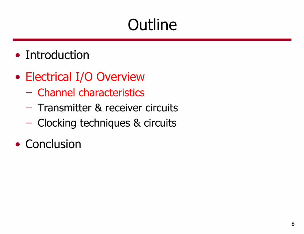
High-Speed Electrical Link System

10
Electrical Backplane Channel
• Frequency dependent loss Dispersion & reflections
• Co-channel interference Far-end (FEXT) & near-end (NEXT) crosstalk
11
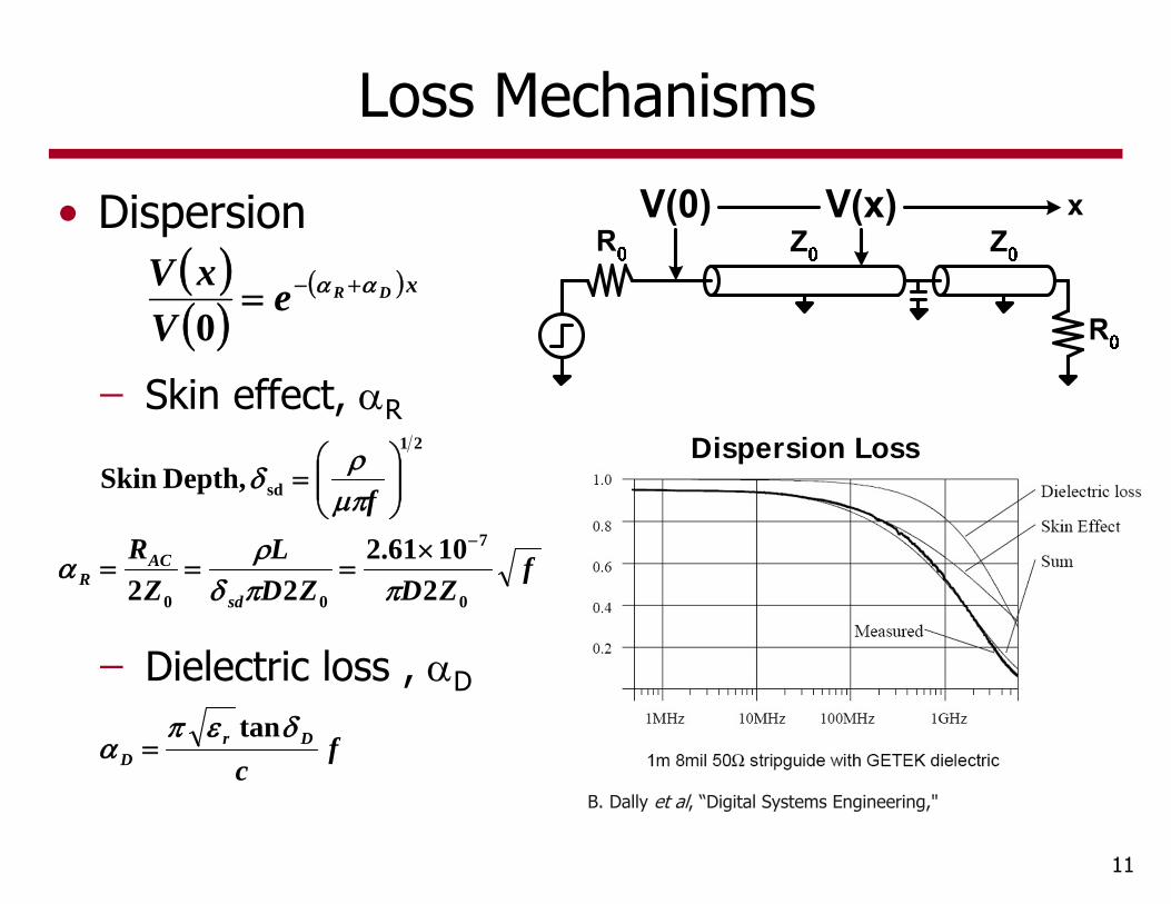
Loss Mechanisms
• Dispersion
Skin effect, R
Dielectric loss , D
xDReV
xV 0
21
sd Depth, Skin
f
fZDZD
LZ
R
sd
ACR
0
7
00 21061.2
22
fc
DrD
tan
Dispersion Loss
B. Dally et al, “Digital Systems Engineering,"

12
Reflections
0
0
ZZZZ
VV
r
r
i
r
• Commonly caused by board via stubs and on-chip termination mismatches
with via stubs

13
Crosstalk
• Occurs mostly in package and board-to-board connectors
• FEXT is attenuated by channel response and has band-pass characteristic
• NEXT directly couples into victim and has high-pass characteristic

14
Channel Performance Impact

15
Channel Performance Impact

16
Outline
• Introduction
• Electrical I/O Overview Channel characteristics Transmitter & receiver circuits Clocking techniques & circuits
• Conclusion

17
Link Speed Limitations• High-speed links can be
limited by both the internal electronics and the channel
• Clock generation and distribution is key circuit bandwidth bottleneck Requires data mux/demux
to use multiple clock phases Passives and/or CML
techniques can extend circuit bandwidth at the expense of area and/or power
• Limited channel bandwidth is typically compensated with equalization circuits
Clock Amplitude Reduction*
*C.-K. Yang, “Design of High-Speed Serial Links in CMOS," 1998.
tFO4 in 90nm ~ 30ps

18
Multiplexing Techniques• Data mux/demux operation
typically employs multiple clock phases
• ½ rate architecture (DDR) is most common Sends a bit on both the rising
and falling edge of one differential clock
50% duty cycle is critical
• Higher multiplexing factors with multiple clock phases further increases output data rate relative to on-chip clock frequency Phase spacing/calibration is
critical
2:1 Mux
8:1 Multiplexing TX*
*C.-K. Yang, “Design of High-Speed Serial Links in CMOS," 1998.
19
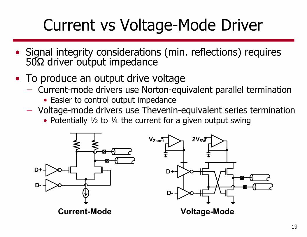
Current vs Voltage-Mode Driver• Signal integrity considerations (min. reflections) requires
50Ω driver output impedance• To produce an output drive voltage
Current-mode drivers use Norton-equivalent parallel termination• Easier to control output impedance
Voltage-mode drivers use Thevenin-equivalent series termination• Potentially ½ to ¼ the current for a given output swing
D+
D-
2VSWVZcont
D+
D-

20
TX FIR Equalization
• TX FIR filter pre-distorts transmitted pulse in order to invert channel distortion at the cost of attenuated transmit signal (de-emphasis)
L
L L
L
L
L
L
L
L
1x 4x 2x 1x
1/4 1 1/2 1/4IDACs&
BiasControl
sgn-1 sgn0 sgn1 sgn2
50Ω
Out-P
Out-N
4:2MUX
2
2
2
21
D0
D1
D2
D3
VDDA=1.2VVDD=1.0V
VDDIO=1.0V
VDDA=1.2V
1
1
1
C2 (5GHz)From on-chip PLL
2
(2.5
Gb/
s)
(10Gb/s)
(5Gb/s)
ESD
L
L L
L
L
L
L
L
L
LL
LL LL
LL
LL
LL
LL
LL
LL
1x 4x 2x 1x
1/4 1 1/2 1/4IDACs&
BiasControl
sgn-1 sgn0 sgn1 sgn2
50Ω
Out-P
Out-N
4:2MUX
2
2
2
21
D0
D1
D2
D3
VDDA=1.2VVDD=1.0V
VDDIO=1.0V
VDDA=1.2V
1
1
1
C2 (5GHz)From on-chip PLL
2
(2.5
Gb/
s)
(10Gb/s)
(5Gb/s)
ESD
2
21010 2101TERM
outRDIDIDIDIV
“A Low Power 10Gb/s Serial Link Transmitter in 90-nm CMOS,” A. Rylyakov et al., CSICS 2005
21
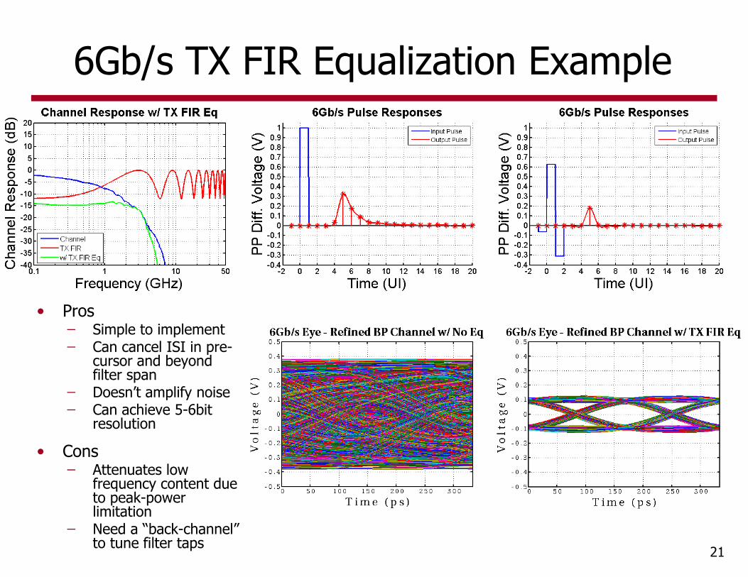
6Gb/s TX FIR Equalization Example
• Pros Simple to implement Can cancel ISI in pre-
cursor and beyond filter span
Doesn’t amplify noise Can achieve 5-6bit
resolution
• Cons Attenuates low
frequency content due to peak-power limitation
Need a “back-channel” to tune filter taps

22
Demultiplexing RX• Input pre-amp followed
by comparator segments Pre-amp may implement
peaking filtering Comparator typically
includes linear-amp & regenerative (positive feedback) latch
• Demultiplexing allows for lower clock frequency relative to data rate and extra regeneration and pre-charge time in comparators
Clk0Clk180
10Gb/s Data
5GHz Clocks
Clk0
Clk180
D[0]
D[1]
Out+Out-
clk
clk clkclk
Din-Din+
23
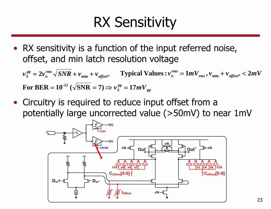
RX Sensitivity• RX sensitivity is a function of the input referred noise,
offset, and min latch resolution voltage
Out+Out-
x2x4x8x16
COffset[4:0]x2 x4 x8 x16
COffset[5:9]
clk
clk clkclk
Din-Din+
IOffset
Clk0
Clk180
D[0]
D[1]
• Circuitry is required to reduce input offset from a potentially large uncorrected value (>50mV) to near 1mV
*min2 offsetrmsn
ppS vvSNRvv mVvvmVv offsetrms
rmsn 2 ,1 :Values Typical *min
17)7SNR( 10BERFor -12pp
ppS mVv
24
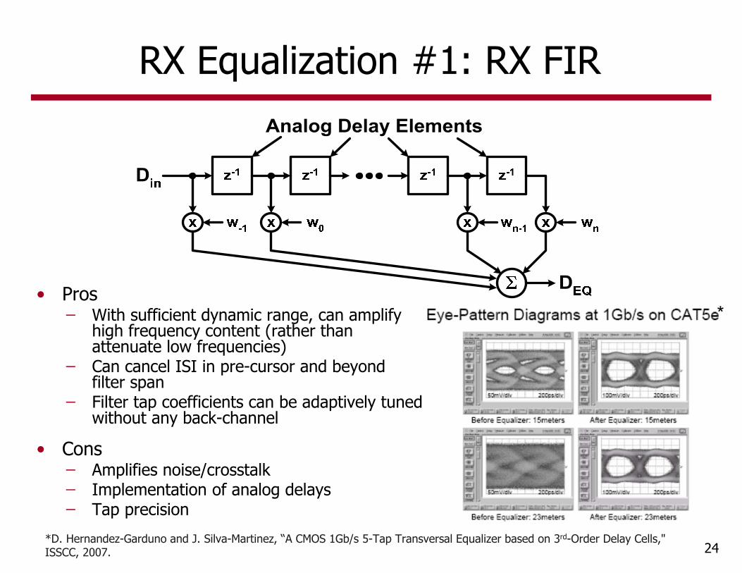
RX Equalization #1: RX FIR
• Pros With sufficient dynamic range, can amplify
high frequency content (rather than attenuate low frequencies)
Can cancel ISI in pre-cursor and beyond filter span
Filter tap coefficients can be adaptively tuned without any back-channel
• Cons Amplifies noise/crosstalk Implementation of analog delays Tap precision
*
*D. Hernandez-Garduno and J. Silva-Martinez, “A CMOS 1Gb/s 5-Tap Transversal Equalizer based on 3rd-Order Delay Cells," ISSCC, 2007.

25
RX Equalization #2: RX CTLE
Din- Din+
Vo-Vo+
• Pros Provides gain and
equalization with low power and area overhead
Can cancel both pre-cursor and long-tail ISI
• Cons Generally limited to 1st
order compensation Amplifies noise/crosstalk PVT sensitivity Can be hard to tune

26
RX Equalization #3: RX DFE
z-1clk
x
w1
z-1x
w2
z-1x
wn-1
z-1x
wn
Din DRX
• Pros No noise and crosstalk
amplification Filter tap coefficients
can be adaptively tuned without any back-channel
• Cons Cannot cancel pre-
cursor ISI Critical feedback timing
path Timing of ISI
subtraction complicates CDR phase detection

27
Outline
• Introduction
• Electrical I/O Overview Channel characteristics Transmitter & receiver circuits Clocking techniques & circuits
• Conclusion

28
Clocking Architecture #1Source Synchronous Clocking
• Common high-speed reference clock is forwarded from TX chip to RX chip
• “Coherent” clocking allows high frequency jitter tracking Jitter frequency lower than delay
difference (typically less than 10bits) can be tracked
Allows power down of phase detection circuitry
• Only periodic acquisition vs continuous tracking
• Requires one extra clock channel• Need good clock receive amplifier as
the forwarded clock can get attenuated by the low pass channel
• Low pass channel causes jitter amplification
*S. Sidiropoulos, “High Performance Inter-Chip Signalling," 1998.
29
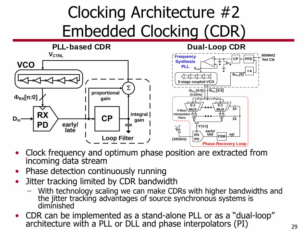
• Clock frequency and optimum phase position are extracted from incoming data stream
• Phase detection continuously running• Jitter tracking limited by CDR bandwidth
With technology scaling we can make CDRs with higher bandwidths and the jitter tracking advantages of source synchronous systems is diminished
• CDR can be implemented as a stand-alone PLL or as a “dual-loop” architecture with a PLL or DLL and phase interpolators (PI)
Clocking Architecture #2Embedded Clocking (CDR)
early/late
VCTRL
integral gain
proportional gain
Din
Loop Filter
RX[n:0]
FSM selearly/late
Phase-Recovery Loop
RXPD
CP
Vctrl
FrequencySynthesis
PLL
5-stage coupled VCO
4
800MHZ Ref ClkPFD
PLL[4:0]
(16Gb/s)
5 Mux/Interpolator
Pairs
5:1 MUX
5:1 MUX
PLL[4:0](3.2GHz)
PLL[0]
15
10
PLL-based CDR Dual-Loop CDR
30
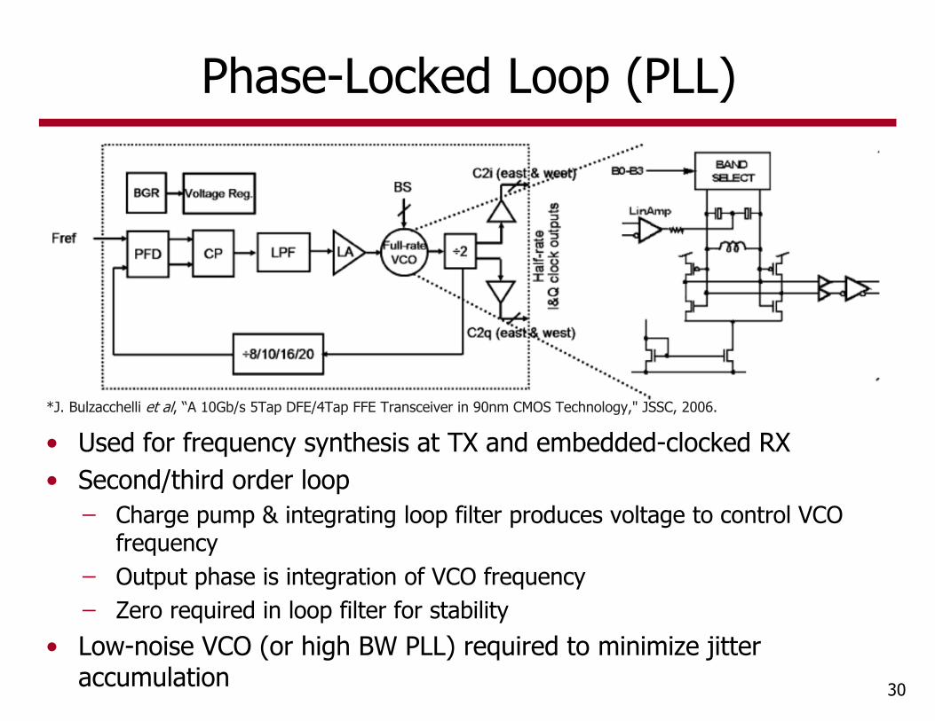
• Used for frequency synthesis at TX and embedded-clocked RX• Second/third order loop
Charge pump & integrating loop filter produces voltage to control VCO frequency
Output phase is integration of VCO frequency Zero required in loop filter for stability
• Low-noise VCO (or high BW PLL) required to minimize jitter accumulation
Phase-Locked Loop (PLL)
*J. Bulzacchelli et al, “A 10Gb/s 5Tap DFE/4Tap FFE Transceiver in 90nm CMOS Technology," JSSC, 2006.

31
Delay-Locked Loop (DLL)
• Typically used to generate multiple clock phases in RX• First order loop guarantees stability• Delay line doesn’t accumulate jitter like a VCO• Difficult to use for frequency synthesis

32
• Interpolators mix between two clock phases to produce the fine resolution clock phases used by the RX samplers
• Critical to limit bandwidth of PI mixing node for good linearity Hard to design over wide frequency range without bandwidth
adjustment and/or input slew-rate control
Phase Interpolator (PI)
*J. Bulzacchelli et al, “A 10Gb/s 5Tap DFE/4Tap FFE Transceiver in 90nm CMOS Technology," JSSC, 2006.

33
Clock Distribution
Architecture Jitter Power Area ComplexityInverter Moderate Moderate Low LowCML Good High Moderate ModerateT-line Good Low Low ModerateResonant T-line Excellent Low High High
*J. Poulton et al, “A 14mW 6.25Gb/s Transceiver in 90nm CMOS," JSSC, 2007.
• Careful clock distribution is required in multi-channel I/O systems
• Different distribution architectures trade-off jitter, power, area, and complexity
Resonant T-line DistributionExample

34
Conclusion• High-speed I/O systems offer challenges in both circuit
and communication system design
• Controlled-impedance drivers are necessary for high-speed signaling
• Achieving good RX sensitivity requires careful front-end noise analysis and sampler offset correction
• Low-noise clock generation, distribution, and recovery is necessary in high-performance serial links


![El Destino de Diez [ECEN]](https://img.dokumen.tips/doc/110x75/563db877550346aa9a93f1f9/el-destino-de-diez-ecen.jpg)