Embed Size (px)
Citation preview
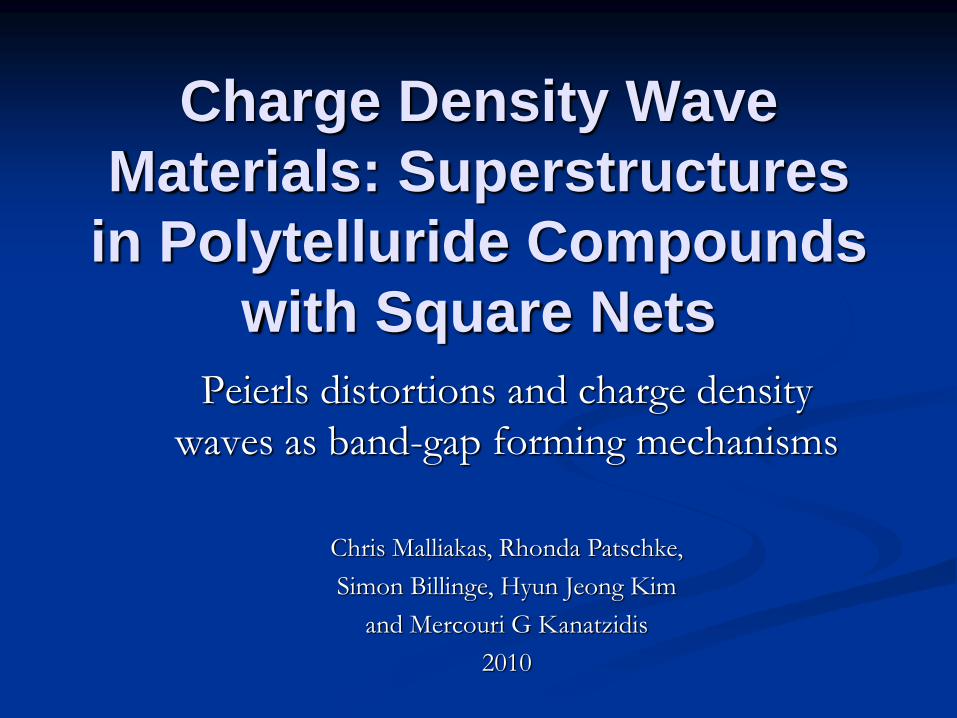
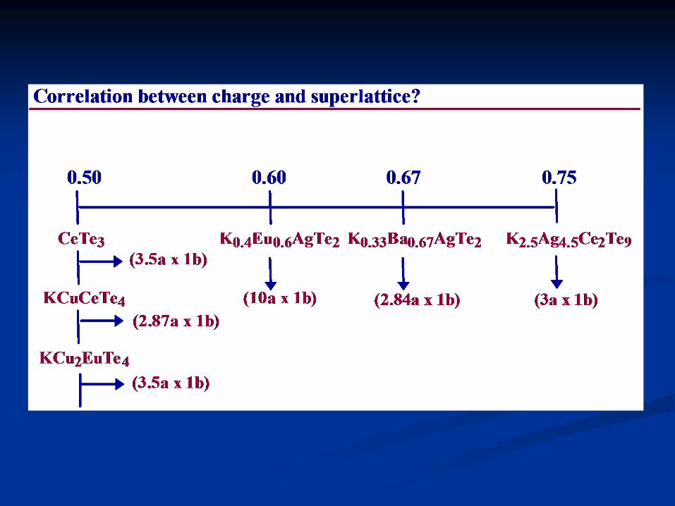
Charge Density Wave
Materials: Superstructures
in Polytelluride Compounds
with Square Nets
Peierls distortions and charge density
waves as band-gap forming mechanisms
Chris Malliakas, Rhonda Patschke,
Simon Billinge, Hyun Jeong Kim
and Mercouri G Kanatzidis
2010
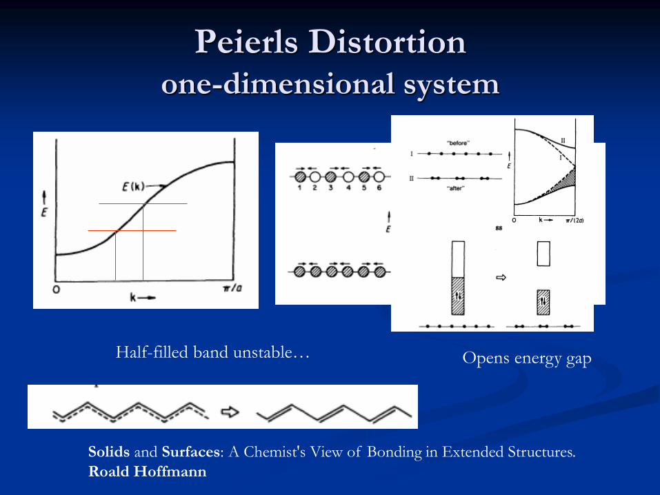
Peierls Distortion one-dimensional system
Solids and Surfaces: A Chemist's View of Bonding in Extended Structures.
Roald Hoffmann
Half-filled band unstable… Opens energy gap
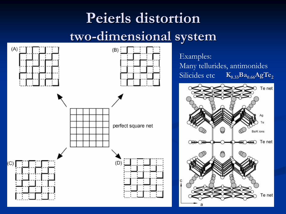
Peierls distortion two-dimensional system
Examples:
Many tellurides, antimonides
Silicides etc K0.33Ba0.66AgTe2
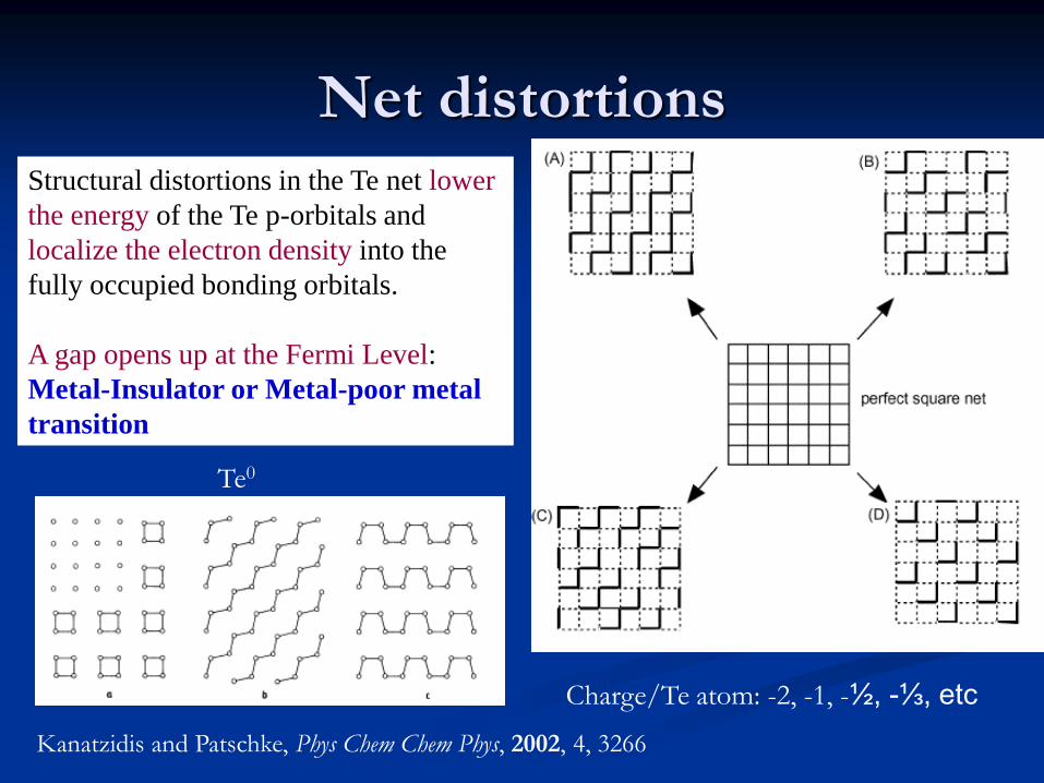
Net distortions Structural distortions in the Te net lower
the energy of the Te p-orbitals and
localize the electron density into the
fully occupied bonding orbitals.
A gap opens up at the Fermi Level:
Metal-Insulator or Metal-poor metal
transition
Kanatzidis and Patschke, Phys Chem Chem Phys, 2002, 4, 3266
Te0
Charge/Te atom: -2, -1, -½, -⅓, etc
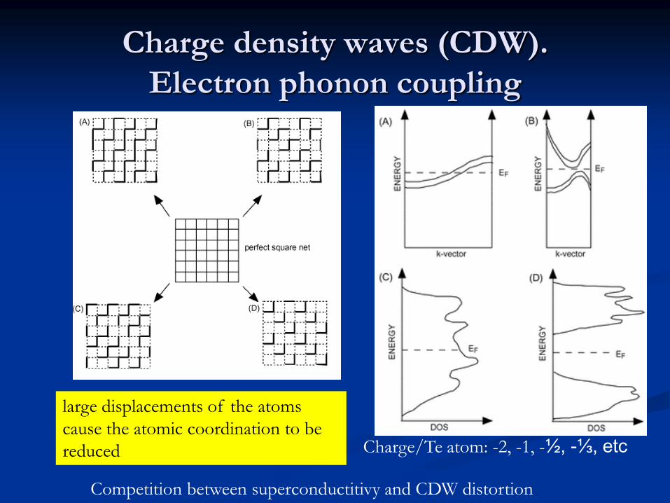
Charge density waves (CDW).
Electron phonon coupling
Competition between superconductitivy and CDW distortion
Charge/Te atom: -2, -1, -½, -⅓, etc
large displacements of the atoms
cause the atomic coordination to be
reduced
Mechanism for forming very narrow
gap semiconductors
Narrow gap semiconductors are of interest as long wavelength detector materials and thermoelectrics
PbTe 0.28 eV, Bi2Te3 0.14 eV, CsBi4Te6 0.08 eV, (Bi0.8Sb0.2) 0.03 eV.
Very narrow gaps (<0.05 eV) are very difficult to design.
may be possible with CDW systems arising from square nets of e.g. Te.
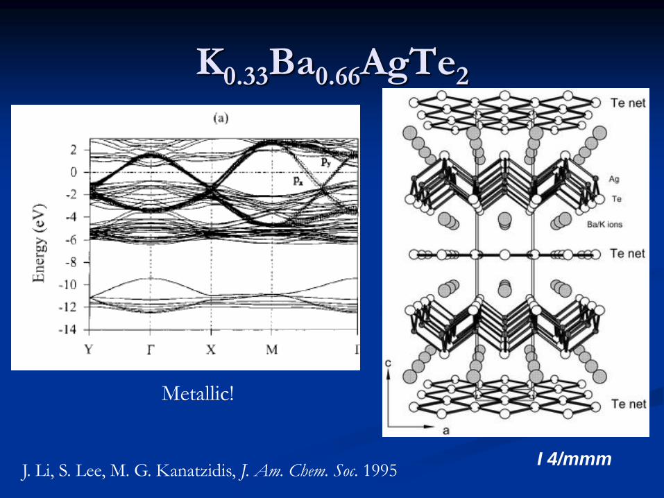
K0.33Ba0.66AgTe2
I 4/mmm
Metallic!
J. Li, S. Lee, M. G. Kanatzidis, J. Am. Chem. Soc. 1995
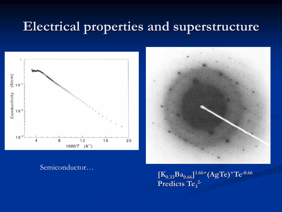
Electrical properties and superstructure
[K0.33Ba0.66]1.66+(AgTe)+Te-0.66
Predicts Te32-
Semiconductor…

Trimers (Te3)2-, bonding (proposed)

Distortion pattern in K0.33Ba0.66AgTe2
Te-0.66 or Te32-
3 Te32- or
1 Te32-, 1 Te5
2- and 1 Te2-
O. Gourdon, J. Hanko, F. Boucher, V. Petricek, M.-H. Whangbo, M. G. Kanatzidis & M Evain, Inorg. Chem. 2000, 39, 1398
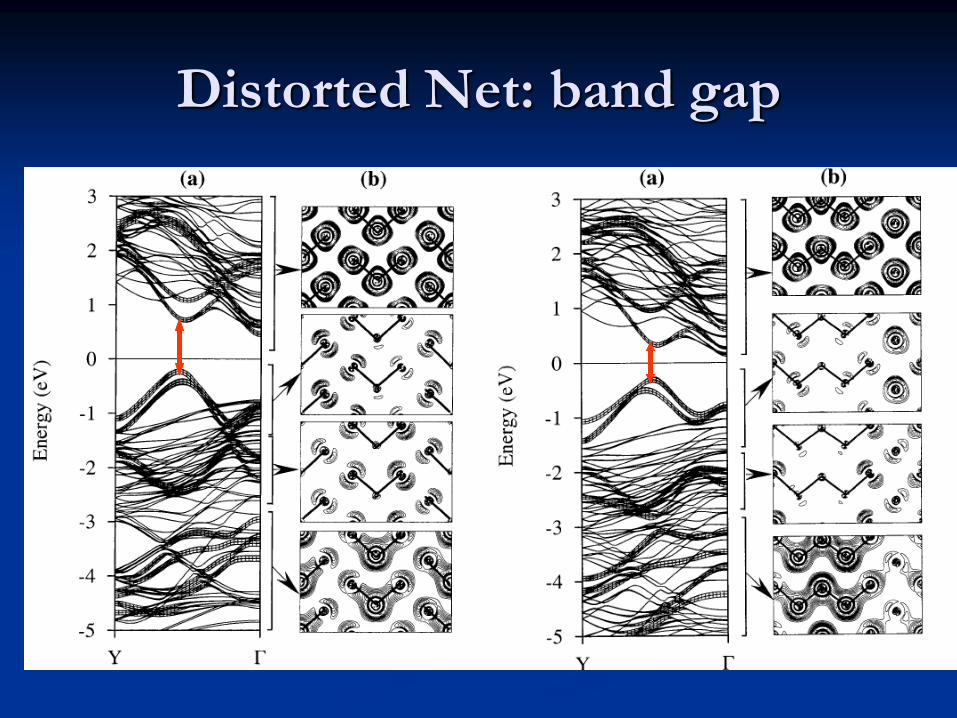
Distorted Net: band gap
a
c
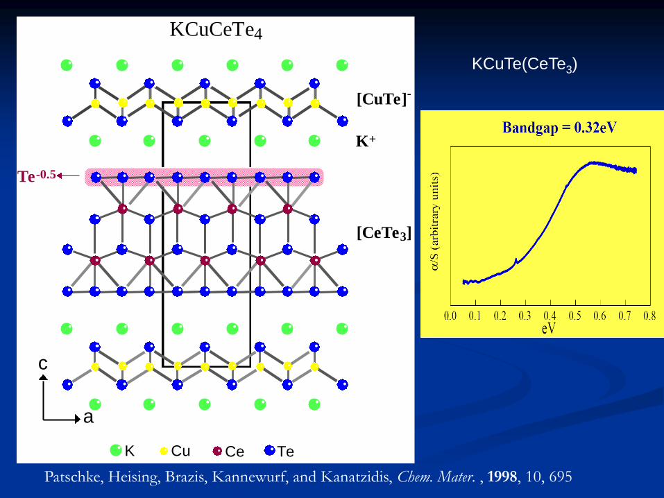
TeK Cu Ce
KCuCeTe4
[CeTe3]
[CuTe]-
K+
Te-0.5
Patschke, Heising, Brazis, Kannewurf, and Kanatzidis, Chem. Mater. , 1998, 10, 695
KCuTe(CeTe3)
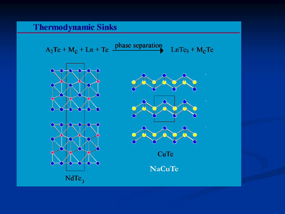
NaCuTe
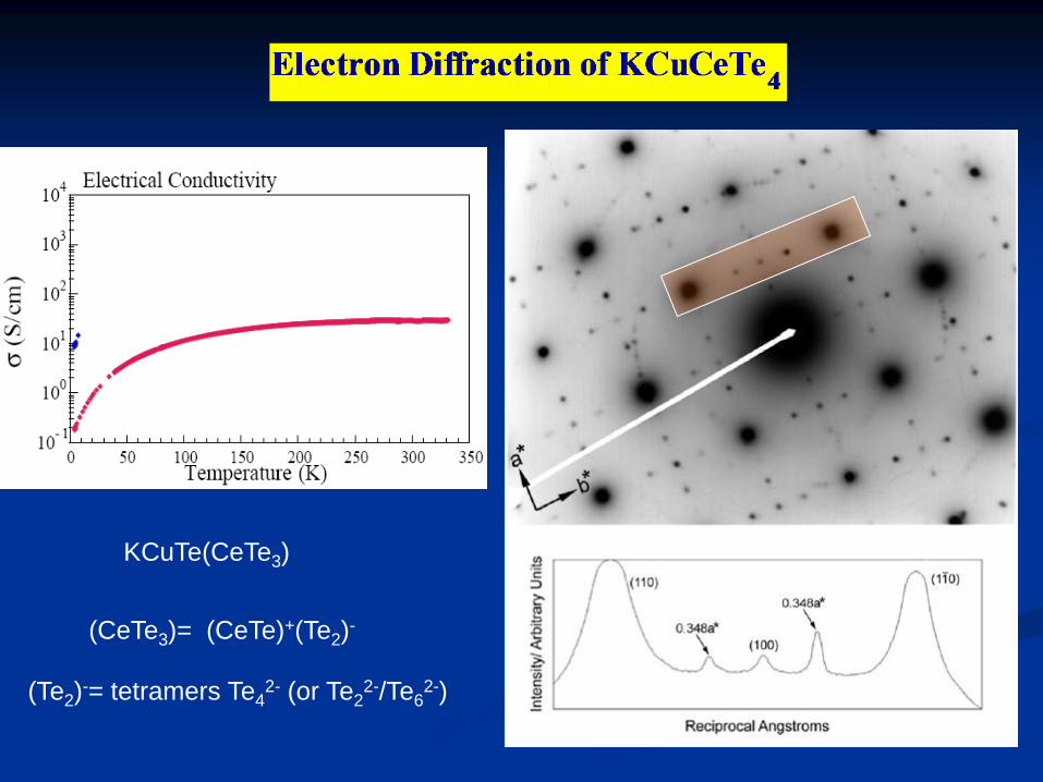
KCuTe(CeTe3)
(CeTe3)= (CeTe)+(Te2)-
(Te2)-= tetramers Te4
2- (or Te22-/Te6
2-)
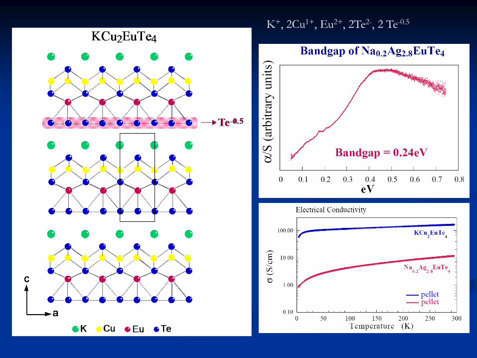
K+, 2Cu1+, Eu2+, 2Te2-, 2 Te-0.5

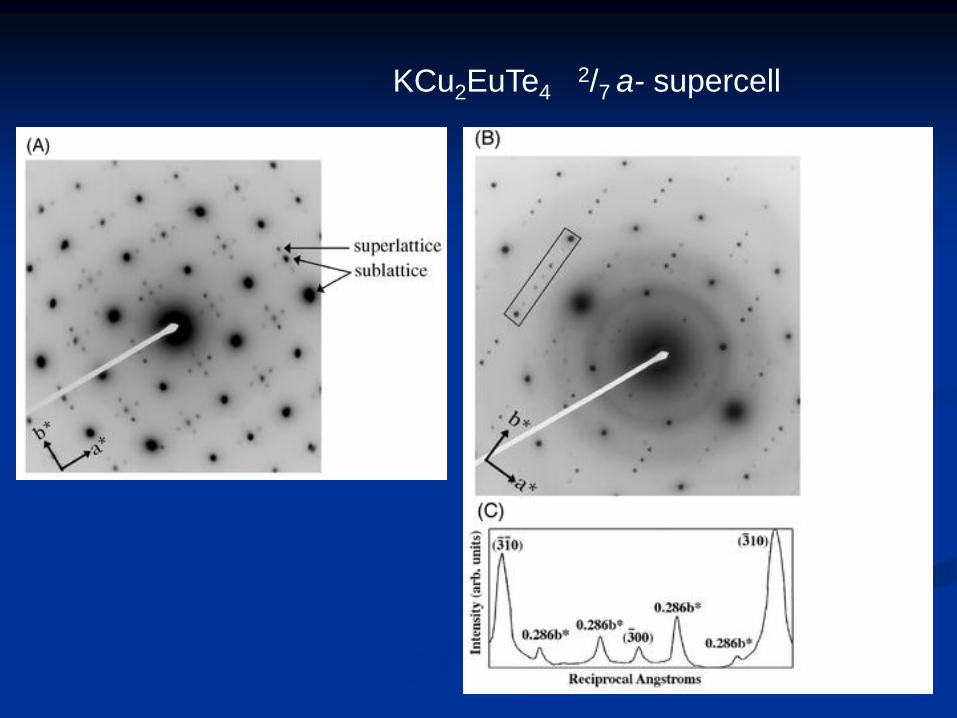
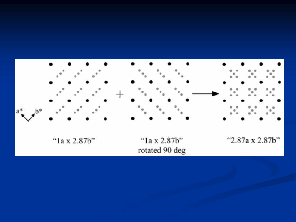
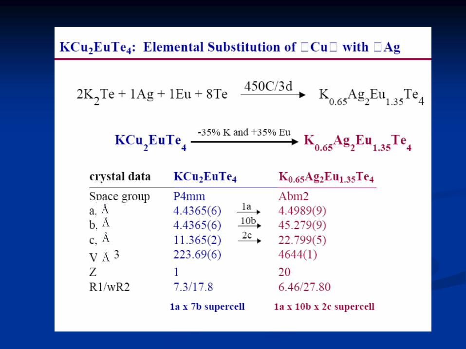
KCu2EuTe4 2/7 a- supercell
Å Å
Å
Å
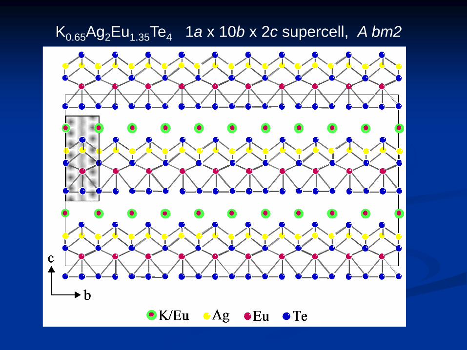
K0.65Ag2Eu1.35Te4 1a x 10b x 2c supercell, A bm2
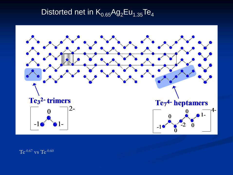
Distorted net in K0.65Ag2Eu1.35Te4
Te-0.67 vs Te-0.60
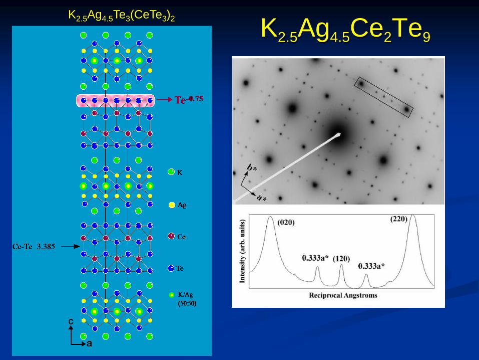
K2.5Ag4.5Ce2Te9
K2.5Ag4.5Te3(CeTe3)2

K2.5Ag4.5La2Te9 and K2.5Ag4.5Ce2Te9
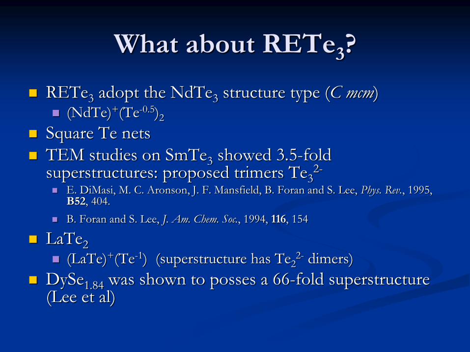
What about RETe3?
RETe3 adopt the NdTe3 structure type (C mcm) (NdTe)+(Te-0.5)2
Square Te nets
TEM studies on SmTe3 showed 3.5-fold superstructures: proposed trimers Te3
2-
E. DiMasi, M. C. Aronson, J. F. Mansfield, B. Foran and S. Lee, Phys. Rev., 1995, B52, 404.
B. Foran and S. Lee, J. Am. Chem. Soc., 1994, 116, 154
LaTe2 (LaTe)+(Te-1) (superstructure has Te2
2- dimers)
DySe1.84 was shown to posses a 66-fold superstructure (Lee et al)
b-
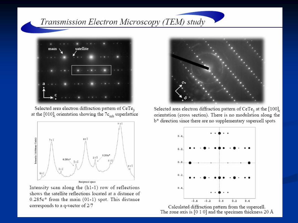

Single Crystal Diffraction Analysis Precession photos
a*
c*
Crystal Data
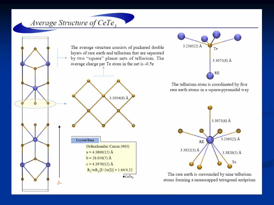
CeTe3
Ama2 (#40)
a = 30.800(8) Å
b = 26.055(7) Å
c = 4.3810(12) Å
R1/wR
2 = 3.82/8.83
PrTe3
NdTe3
SmTe3
GdTe3
Ama2 (#40)
a = 30.640(8) Å
b = 25.915(7) Å
c = 4.3598(11) Å
R1/wR
2 = 4.98/14.69
Ama2 (#40)
a = 30.561(6) Å
b = 25.859(5) Å
c = 4.3563(9) Å
R1/wR
2 = 4.81/12.43
Ama2 (#40)
a = 30.383(8) Å
b = 25.676(6) Å
c = 4.3341(11) Å
R1/wR
2 = 5.30/20.28
Ama2 (#40)
a = 30.307(7) Å
b = 25.573(6) Å
c = 4.3162(9) Å
R1wR2 = 5.44/10.54
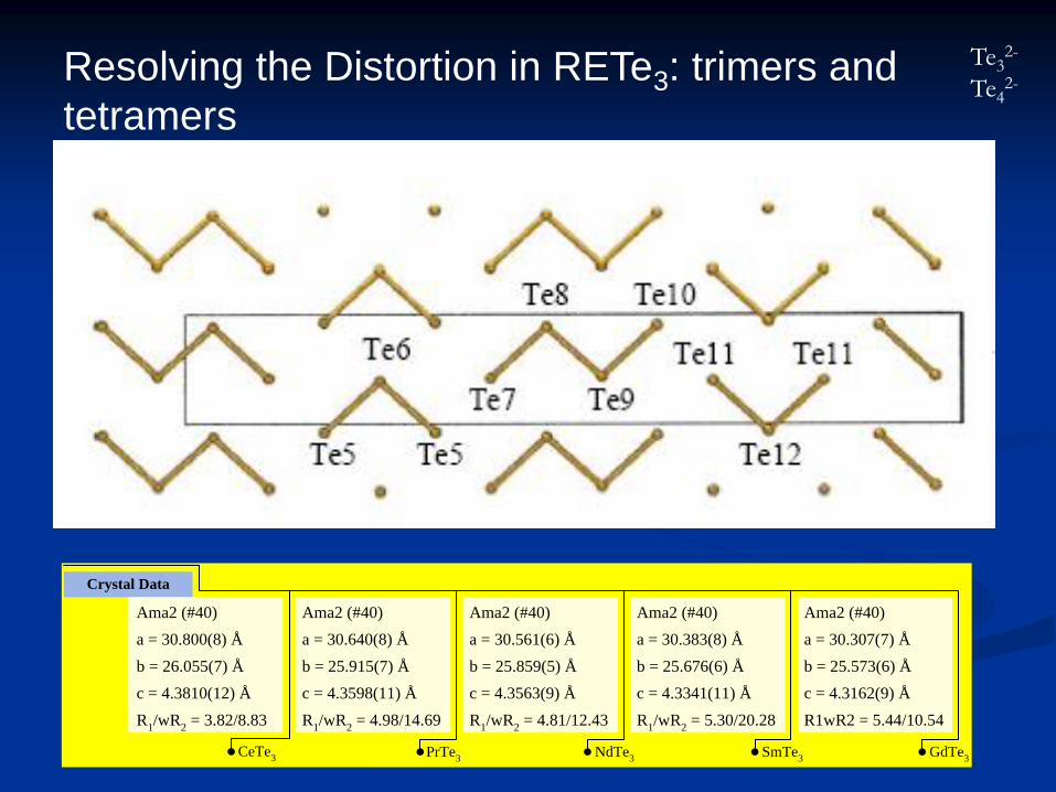
Resolving the Distortion in RETe3: trimers and
tetramers
Te32-
Te42-

Crystal Data
CeTe3
Ama2 (#40)
a = 30.800(8) Å
b = 26.055(7) Å
c = 4.3810(12) Å
R1/wR
2 = 3.82/8.83
PrTe3
NdTe3
SmTe3
GdTe3
Ama2 (#40)
a = 30.640(8) Å
b = 25.915(7) Å
c = 4.3598(11) Å
R1/wR
2 = 4.98/14.69
Ama2 (#40)
a = 30.561(6) Å
b = 25.859(5) Å
c = 4.3563(9) Å
R1/wR
2 = 4.81/12.43
Ama2 (#40)
a = 30.383(8) Å
b = 25.676(6) Å
c = 4.3341(11) Å
R1/wR
2 = 5.30/20.28
Ama2 (#40)
a = 30.307(7) Å
b = 25.573(6) Å
c = 4.3162(9) Å
R1wR2 = 5.44/10.54
Resolving the Distortion in RETe3
The supercell has a c=7csub
axis. The modulation is
mostly located in the Te net which results a wide
distribution of distances between the atoms.
For CeTe3 the minimum distance is 2.94(2) Å and the
maximum 3.26(3) Å with an average of 3.11(3) Å
With bonding cutoff of 3.100 Å
Bonding cutoff less than 3.020 Å the net reveals V-
shaped trimers and N-shaped tetramers.
Te32-
Te42-
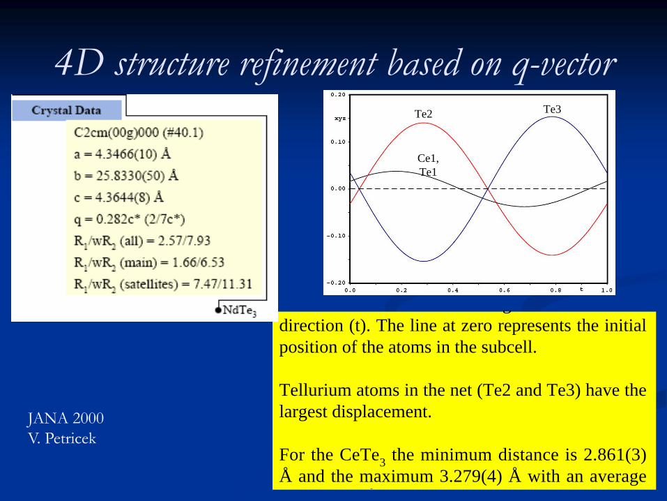
4D structure refinement based on q-vector
Position of all atoms along the modulation
direction (t). The line at zero represents the initial
position of the atoms in the subcell.
Tellurium atoms in the net (Te2 and Te3) have the
largest displacement.
For the CeTe3 the minimum distance is 2.861(3)
Å and the maximum 3.279(4) Å with an average
of 3.069(5) Å
Te2 Te3
Ce1,
Te1
JANA 2000
V. Petricek
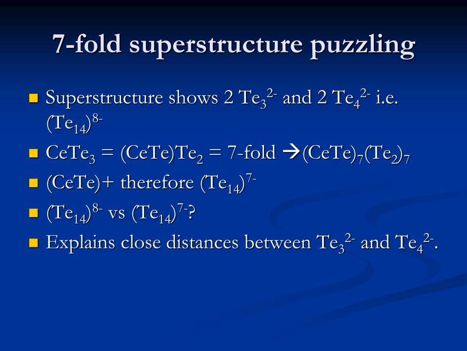
7-fold superstructure puzzling
Superstructure shows 2 Te32- and 2 Te4
2- i.e.
(Te14)8-
CeTe3 = (CeTe)Te2 = 7-fold (CeTe)7(Te2)7
(CeTe)+ therefore (Te14)7-
(Te14)8- vs (Te14)
7-?
Explains close distances between Te32- and Te4
2-.

Are distortions characteristic of the
bulk?
Simple powder diffraction inadequate to detect
superstructure
PDF: a total scattering technique
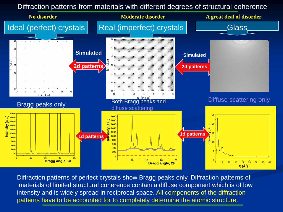
Ideal (perfect) crystals
Bragg peaks only Both Bragg peaks and
diffuse scattering
5 10 15 20 25
0
200
400
600
800
1000
1200
1400
1600
1800
2000
Inte
ns
ity
(a
.u.)
Bragg angle, 2q
Real (imperfect) crystals
Diffraction patterns of perfect crystals show Bragg peaks only. Diffraction patterns of
materials of limited structural coherence contain a diffuse component which is of low
intensity and is widely spread in reciprocal space. All components of the diffraction
patterns have to be accounted for to completely determine the atomic structure.
No disorder Moderate disorder A great deal of disorder
Diffuse scattering only
Simulated
2d patterns
Glass
0 5 10 15 20 25 30 35 400
5
10
15
20
25
Inte
ns
ity
, a
.u.
Q (Å-1)
5 10 15 20 25
0
200
400
600
800
1000
1200
1400
1600
1800
2000
Inte
nsit
y (
a.u
.)
Bragg angle, 2q
Diffraction patterns from materials with different degrees of structural coherence
1d patterns 1d patterns
Simulated
2d patterns
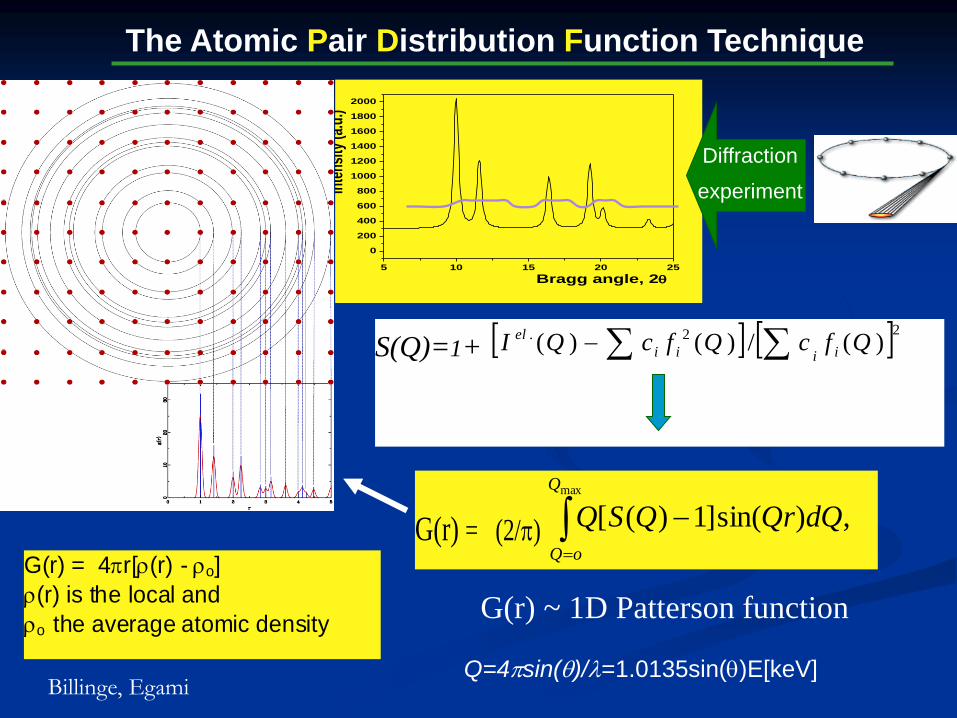
The Atomic Pair Distribution Function Technique
Q=4sin(q)/=1.0135sin(q)E[keV]
S(Q)=1+ 22. )(/)()( QfcQfcQI iiii
el
G(r) = (2/)
max
,)sin(]1)([
Q
oQ
dQQrQSQ
G(r) = 4r[(r) - o]
(r) is the local and
o the average atomic density
5 10 15 20 25
0
200
400
600
800
1000
1200
1400
1600
1800
2000
Inte
nsity
(a.u
.)
Bragg angle, 2q
Diffraction
experiment
G(r) ~ 1D Patterson function
Billinge, Egami
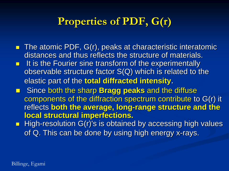
Properties of PDF, G(r)
The atomic PDF, G(r), peaks at characteristic interatomic distances and thus reflects the structure of materials.
It is the Fourier sine transform of the experimentally observable structure factor S(Q) which is related to the
elastic part of the total diffracted intensity. Since both the sharp Bragg peaks and the diffuse
components of the diffraction spectrum contribute to G(r) it reflects both the average, long-range structure and the local structural imperfections.
High-resolution G(r)'s is obtained by accessing high values
of Q. This can be done by using high energy x-rays.
Billinge, Egami
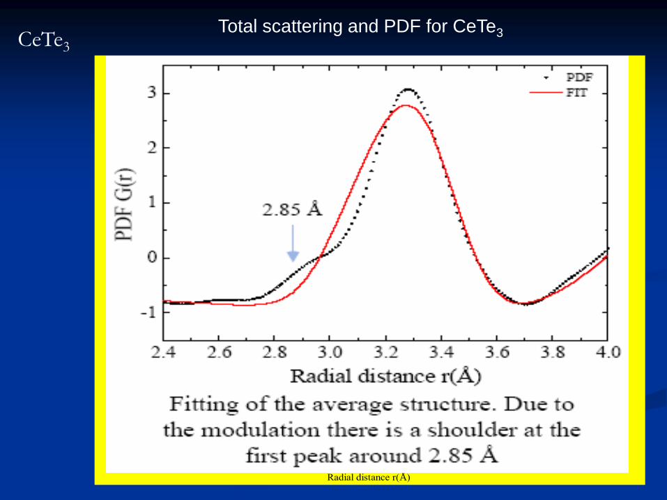
Total scattering and PDF for CeTe3
WPair Distribution Function (PDF) analysisW
1 2 3 4 5 6 7 8 9 10 11 12 13 14 15 16 17 18 19 20
-3
-2
-1
0
1
2
3
4
5
0 2 4 6 8 10 12 14 16 18 20 22 24-4
-2
0
2
4
6
8
10
12
0 5 10 15 20 25 300
2000
4000
6000
8000
10000
12000
14000
16000
18000
20000
22000
model
fit
PD
F G
(r)
Radial distance r(Å)
Wavevector Q(Å-1
)
Q[S
(q)-
1]
In
ten
sity
(cp
s)
2θ (degree)
X-ray and neutron powder diffraction experiment to
measure over a wide range of momentum transfer, Q
Q’s of > 30 A-1 are desirable sin4Q
Real-space resolution of maxQr
1)(
)()()(
2
2
Qfc
QfcQIQS
ii
ii
coh
Data correction for experimental effects (sample absorption,
multiple scattering, etc.) and normalization by f(Q)2122
)(Qf )(Qf
It can be calculated directly from a structure model using
])([4)( 0 rrrG
)(
)0(
)0()0(14)(
20 rrf
ff
rrrG
max
0
)sin(]1)([2)(
Q
Q
dQQrQSQrG
Fourier transform of Q[S(Q)-1]
CeTe3

Local structure: PDF versus
Crystallography
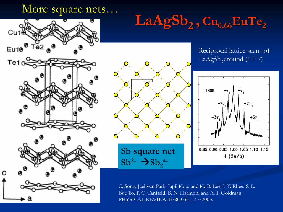
LaAgSb2 , Cu0.66EuTe2
Reciprocal lattice scans of
LaAgSb2 around (1 0 7)
C. Song, Jaehyun Park, Japil Koo, and K.-B. Lee, J. Y. Rhee, S. L.
Bud’ko, P. C. Canfield, B. N. Harmon, and A. I. Goldman,
PHYSICAL REVIEW B 68, 035113 ~2003.
Sb square net
Sb2- Sb24-
More square nets…
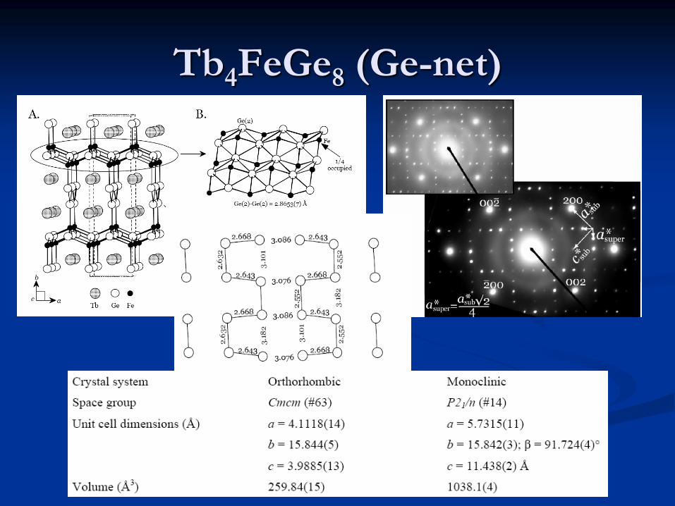
Tb4FeGe8 (Ge-net)
Conclusions
Square nets inherently unstable
Square nets of Te obey the octet rule.
Permanent CDW materials a potential new source of
narrow gap semiconductors
New way to design extremely narrow gap materials
Known modulated Te-net compounds need to be
solved.
Many “ideal” square net compounds need to be re-
examined.