Embed Size (px)
Citation preview
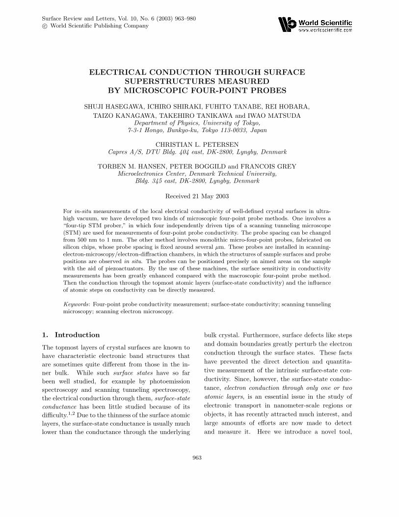
Surface Review and Letters, Vol. 10, No. 6 (2003) 963–980c© World Scientific Publishing Company
ELECTRICAL CONDUCTION THROUGH SURFACE
SUPERSTRUCTURES MEASURED
BY MICROSCOPIC FOUR-POINT PROBES
SHUJI HASEGAWA, ICHIRO SHIRAKI, FUHITO TANABE, REI HOBARA,
TAIZO KANAGAWA, TAKEHIRO TANIKAWA and IWAO MATSUDADepartment of Physics, University of Tokyo,
7-3-1 Hongo, Bunkyo-ku, Tokyo 113-0033, Japan
CHRISTIAN L. PETERSENCapres A/S, DTU Bldg. 404 east, DK-2800, Lyngby, Denmark
TORBEN M. HANSEN, PETER BOGGILD and FRANCOIS GREYMicroelectronics Center, Denmark Technical University,
Bldg. 345 east, DK-2800, Lyngby, Denmark
Received 21 May 2003
For in-situ measurements of the local electrical conductivity of well-defined crystal surfaces in ultra-high vacuum, we have developed two kinds of microscopic four-point probe methods. One involves a“four-tip STM prober,” in which four independently driven tips of a scanning tunneling microscope(STM) are used for measurements of four-point probe conductivity. The probe spacing can be changedfrom 500 nm to 1 mm. The other method involves monolithic micro-four-point probes, fabricated onsilicon chips, whose probe spacing is fixed around several µm. These probes are installed in scanning-electron-microscopy/electron-diffraction chambers, in which the structures of sample surfaces and probepositions are observed in situ. The probes can be positioned precisely on aimed areas on the samplewith the aid of piezoactuators. By the use of these machines, the surface sensitivity in conductivitymeasurements has been greatly enhanced compared with the macroscopic four-point probe method.Then the conduction through the topmost atomic layers (surface-state conductivity) and the influenceof atomic steps on conductivity can be directly measured.
Keywords: Four-point probe conductivity measurement; surface-state conductivity; scanning tunnelingmicroscopy; scanning electron microscopy.
1. Introduction
The topmost layers of crystal surfaces are known to
have characteristic electronic band structures that
are sometimes quite different from those in the in-
ner bulk. While such surface states have so far
been well studied, for example by photoemission
spectroscopy and scanning tunneling spectroscopy,
the electrical conduction through them, surface-state
conductance has been little studied because of its
difficulty.1,2 Due to the thinness of the surface atomic
layers, the surface-state conductance is usually much
lower than the conductance through the underlying
bulk crystal. Furthermore, surface defects like steps
and domain boundaries greatly perturb the electron
conduction through the surface states. These facts
have prevented the direct detection and quantita-
tive measurement of the intrinsic surface-state con-
ductivity. Since, however, the surface-state conduc-
tance, electron conduction through only one or two
atomic layers, is an essential issue in the study of
electronic transport in nanometer-scale regions or
objects, it has recently attracted much interest, and
large amounts of efforts are now made to detect
and measure it. Here we introduce a novel tool,
963
964 S. Hasegawa et al.
microscopic four-point probes, and demonstrate their
effectiveness for such purposes.3–7
Before going into the details, we should describe
previous trials with macroscopic four-probe methods
in measuring the electrical conductance of atomic
layers of crystal surfaces and/or monolayer-range
thin films. The conductance of metal atomic lay-
ers on insulating substrates was frequently mea-
sured in relation to the growth style and morphol-
ogy of atomic layers.8–13 Those studies have revealed
intriguing phenomena, such as classical/quantum
size effects, insulator-to-metal transition, oscillatory
changes in the sign of Hall coefficients and in the
critical temperature of the superconductivity of the
metal films as a function of the film thickness and
atomic structures. These films are basically assumed
to be just “thinned bulk crystals,” having the same
electronic band structures as the bulk crystals.
The conductance of surface-state bands of bulk
crystals, on the other hand, was measured in several
different ways. One was by observing a conduc-
tance increase due to carrier doping into a surface-
state band by adsorbates on the surface, which
was revealed by combing the conductance mea-
surements with photoemission spectroscopy for the
band-structure measurements.1,2,14 The observed
conductance change was separated from the bulk
conductance by taking into account the change in
surface-state bands. Another way to extract the
surface-state conductance was to use a so-called SOI
(semiconductor-on-insulator) crystal where the sub-
strate conductance was effectively negligible due to
its thinness.15 This was successfully employed in de-
tecting a conductance change due to a phase transi-
tion of the surface structure. Those results, achieved
by using macroscopic four-point probes with
1–10 mm probe spacing, needed some efforts to elim-
inate the conductance of substrate bulks.
A unique technique, so-called scanning poten-
tiometry using a single-tip scanning tunneling micro-
scope (STM), was employed to measure the surface-
state conductance.16 Due to a voltage drop by a finite
resistance of the sample surface, the STM images
showed characteristic contrasts, which were com-
pared with simulation results to deduce the surface-
state conductance. Another example in detecting
the surface-state conductance using STM is leakage-
current measurements at point contacts between the
STM tip and sample surfaces.17 Due to a Schottky
barrier between the STM tip and a silicon substrate,
the leak current was attributed to the current flowing
along the surface-state band. In those measurements
using a single-tip STM, one needed some simulation
or assumption to quantify the results of conductance.
A four-probe method is the most direct and com-
mon one for measuring the electrical conductance of
samples. So we first briefly introduce the principle of
the four-point probe method and electrical conduc-
tion near a semiconductor surface, and then explain
why a microscopic four-point probe is needed to de-
tect and measure the surface-state conductance.
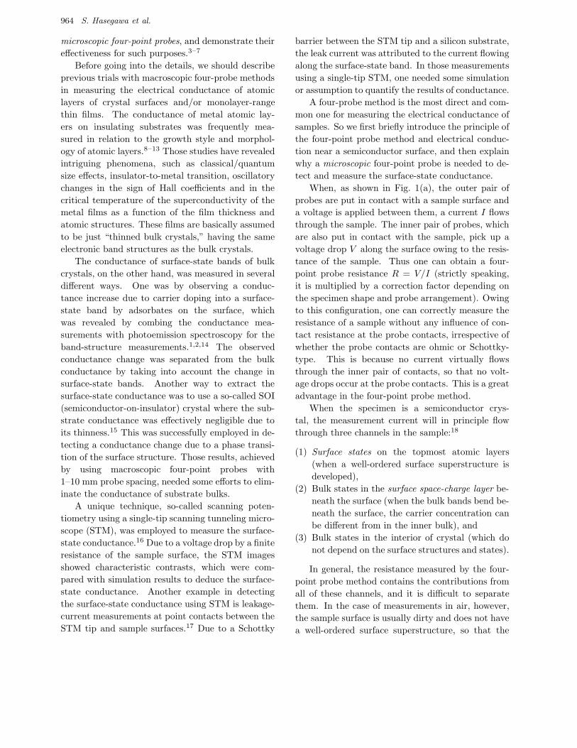
When, as shown in Fig. 1(a), the outer pair of
probes are put in contact with a sample surface and
a voltage is applied between them, a current I flows
through the sample. The inner pair of probes, which
are also put in contact with the sample, pick up a
voltage drop V along the surface owing to the resis-
tance of the sample. Thus one can obtain a four-
point probe resistance R = V/I (strictly speaking,
it is multiplied by a correction factor depending on
the specimen shape and probe arrangement). Owing
to this configuration, one can correctly measure the
resistance of a sample without any influence of con-
tact resistance at the probe contacts, irrespective of
whether the probe contacts are ohmic or Schottky-
type. This is because no current virtually flows
through the inner pair of contacts, so that no volt-
age drops occur at the probe contacts. This is a great
advantage in the four-point probe method.
When the specimen is a semiconductor crys-
tal, the measurement current will in principle flow
through three channels in the sample:18
(1) Surface states on the topmost atomic layers
(when a well-ordered surface superstructure is
developed),
(2) Bulk states in the surface space-charge layer be-
neath the surface (when the bulk bands bend be-
neath the surface, the carrier concentration can
be different from in the inner bulk), and
(3) Bulk states in the interior of crystal (which do
not depend on the surface structures and states).
In general, the resistance measured by the four-
point probe method contains the contributions from
all of these channels, and it is difficult to separate
them. In the case of measurements in air, however,
the sample surface is usually dirty and does not have
a well-ordered surface superstructure, so that the
Electrical Conduction Through Surface Superstructures 965
Fig. 1. (a) Macro- and (b) micro-four-point probe methods to measure electrical conductance. The distribution ofcurrent flowing through a semiconductor specimen is schematically drawn.
measured resistance is interpreted to be only the bulk
value. But under special conditions where the bands
bend sharply under the surface to produce a carrier
accumulation layer, or in ultrahigh vacuum (UHV)
where the sample crystal has a well-ordered surface
superstructure with a conductive surface-state band,
the contributions from the surface layers cannot be
ignored. Even under such situations, however, the
surface contributions have been considered to be very
small, because, as shown in Fig. 1(a), the measure-
ment current flows mainly through the underlying
bulk in the case of macroscopic probe spacing.
If, as shown in Fig. 1(b), one makes the probe
spacing as small as the thickness of the space-charge
layer or less than it, the measurement current will
mainly flow through the surface region, which di-
minishes the bulk contribution in conductance mea-
surement. This microscopic four-point probe method
thus has a higher surface sensitivity. However, this
picture looks too naıve, because the real current dis-
tribution may be complicated due to a possible bar-
rier between the surface state and bulk state and/or
a possible pn junction between the surface space-
charge layer and underlying bulk state. But the
experimental results described below show qualita-
tively the validity of this intuitive picture in Fig. 1.
Microscopic four-point probes have another ad-
vantage: they enable local measurements by select-
ing the area of concern with the aid of microscopes,
so that the influence of observable defects can be
avoided or intentionally included. Furthermore, by
scanning the probes laterally on the sample surface,
one can obtain a map of conductivity with a high
spatial resolution.19
Here, two kinds of microscopic four-point probes
are introduced with some preliminary data.
2. Independently Driven Four-Tip
STM Prober
2.1. Apparatus
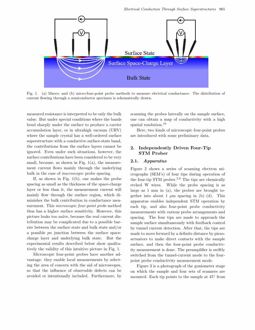
Figure 2 shows a series of scanning electron mi-
crographs (SEM’s) of four tips during operation of
the four-tip STM prober.5,6 The tips are chemically
etched W wires. While the probe spacing is as
large as 1 mm in (a), the probes are brought to-
gether into about 1 µm spacing in (b)–(d). This
apparatus enables independent STM operation by
each tip, and also four-point probe conductivity
measurements with various probe arrangements and
spacing. The four tips are made to approach the
sample surface simultaneously with feedback control
by tunnel current detection. After that, the tips are
made to move forward by a definite distance by piezo-
actuators to make direct contacts with the sample
surface, and then the four-point probe conductiv-
ity measurement is done. The preamplifier is swiftly
switched from the tunnel-current mode to the four-
point probe conductivity measurement mode.
Figure 3 is a photograph of the goniometer stage
on which the sample and four sets of scanners are
mounted. Each tip points to the sample at 45 from
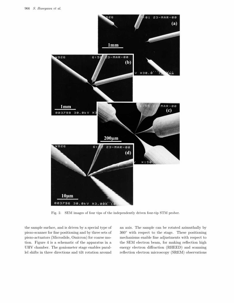
966 S. Hasegawa et al.
Fig. 2. SEM images of four tips of the independently driven four-tip STM prober.
the sample surface, and is driven by a special type of
piezo-scanner for fine positioning and by three sets of
piezo-actuators (Microslide, Omicron) for coarse mo-
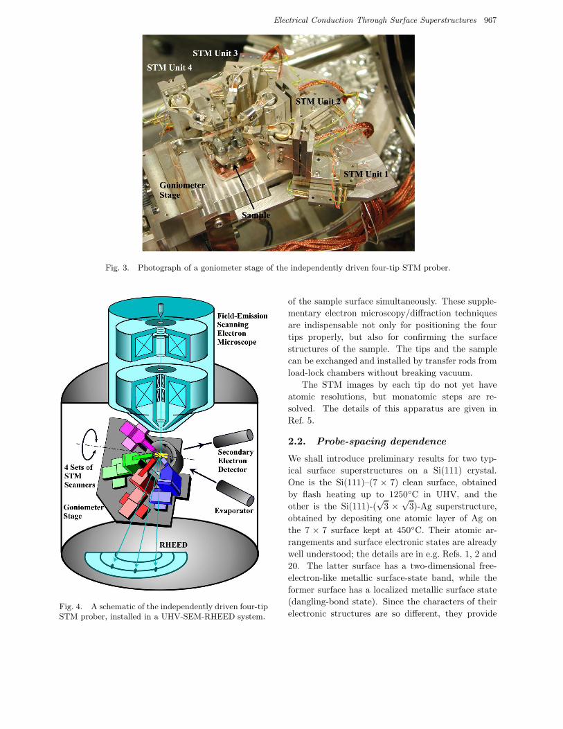
tion. Figure 4 is a schematic of the apparatus in a
UHV chamber. The goniometer stage enables paral-
lel shifts in three directions and tilt rotation around
an axis. The sample can be rotated azimuthally by
360 with respect to the stage. These positioning
mechanisms enable fine adjustments with respect to
the SEM electron beam, for making reflection high
energy electron diffraction (RHEED) and scanning
reflection electron microscopy (SREM) observations
Electrical Conduction Through Surface Superstructures 967
Fig. 3. Photograph of a goniometer stage of the independently driven four-tip STM prober.
Fig. 4. A schematic of the independently driven four-tipSTM prober, installed in a UHV-SEM-RHEED system.
of the sample surface simultaneously. These supple-
mentary electron microscopy/diffraction techniques
are indispensable not only for positioning the four
tips properly, but also for confirming the surface
structures of the sample. The tips and the sample
can be exchanged and installed by transfer rods from
load-lock chambers without breaking vacuum.
The STM images by each tip do not yet have
atomic resolutions, but monatomic steps are re-
solved. The details of this apparatus are given in
Ref. 5.
2.2. Probe-spacing dependence
We shall introduce preliminary results for two typ-
ical surface superstructures on a Si(111) crystal.
One is the Si(111)–(7 × 7) clean surface, obtained
by flash heating up to 1250C in UHV, and the
other is the Si(111)-(√
3 ×√
3)-Ag superstructure,
obtained by depositing one atomic layer of Ag on
the 7 × 7 surface kept at 450C. Their atomic ar-
rangements and surface electronic states are already
well understood; the details are in e.g. Refs. 1, 2 and
20. The latter surface has a two-dimensional free-
electron-like metallic surface-state band, while the
former surface has a localized metallic surface state
(dangling-bond state). Since the characters of their
electronic structures are so different, they provide
968 S. Hasegawa et al.
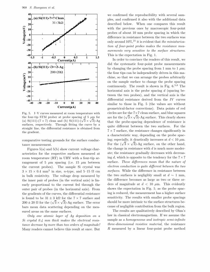
Fig. 5. I–V curves measured at room temperature withthe four-tip STM prober at probe spacing of 5 µm for(a) Si(111)-(7 × 7) clean and (b) Si(111)-(
√3 ×
√3)-Ag
surfaces, respectively. Through fitting the curve by astraight line, the differential resistance is obtained fromthe gradient.
comparative testing grounds for the surface conduc-
tance measurement.
Figures 5(a) and 5(b) show current–voltage char-
acteristics for the respective surfaces measured at
room temperature (RT) in UHV with a four-tip ar-
rangement of 5 µm spacing (i.e. 15 µm between
the current probes). The sample Si crystal was
3 × 15 × 0.4 mm3 in size, n-type, and 5–15 Ω cm
in bulk resistivity. The voltage drop measured by
the inner pair of probes (in the vertical axis) is lin-
early proportional to the current fed through the
outer pair of probes (in the horizontal axis). From
the gradients of the curves, the differential resistance
is found to be 31 ± 3 kΩ for the 7 × 7 surface and
200± 20 Ω for the (√
3×√
3)-Ag surface. The error
bars mean data scattering depending on the mea-
sured areas on the same surfaces.
Only one atomic layer of Ag deposition on a
Si crystal 0.4 mm thick makes the electrical resis-
tance decrease by more than two orders of magnitude!
Many readers cannot believe this result at once. But
we confirmed the reproducibility with several sam-
ples, and confirmed it also with the additional data
described below. When one compares this result
with the previous ones by macroscopic four-point
probes of about 10 mm probe spacing in which the
difference in resistance between the two surfaces was
only around 10%,21 it is evident that the miniaturiza-
tion of four-point probes makes the resistance mea-
surements very sensitive to the surface structures.
This is the expectation in Fig. 1.
In order to convince the readers of this result, we
did the systematic four-point probe measurements
by changing the probe spacing from 1 mm to 1 µm;
the four tips can be independently driven in this ma-
chine, so that we can arrange the probes arbitrarily
on the sample surface to change the probe spacing
continuously. The result is shown in Fig. 6.5,6 The
horizontal axis is the probe spacing d (spacing be-
tween the two probes), and the vertical axis is the
differential resistance derived from the IV curves
similar to those in Fig. 5 (the values are without
geometrical-factor corrections). Data points of red
circles are for the 7×7 clean surface, and blue squares
are for the (√
3×√
3)-Ag surface. This clearly shows
that the probe-spacing dependence of resistance is
quite different between the two surfaces. For the
7 × 7 surface, the resistance changes significantly in
a characteristic way, depending on the probe spac-
ing; especially, it drastically increases at d < 10 µm.
For the (√
3 ×√
3)-Ag surface, on the other hand,
the change in resistance with d is much more moder-
ate; the resistance gradually decreases with decreas-
ing d, which is opposite to the tendency for the 7×7
surface. These differences mean that the nature of
electron conduction is quite different between the two
surfaces. While the difference in resistance between
the two surfaces is negligibly small at d ∼ 1 mm,
the difference becomes as large as two or three or-
ders of magnitude at d < 10 µm. This evidently
shows the expectation in Fig. 1; as the probe spac-
ing is reduced, the measurement has a higher surface
sensitivity. The results with smaller probe spacings
should be more intrinsic to the surface structures be-
cause of negligible contribution from the bulk region.
The results are qualitatively described by Ohm’s
law in classical electromagnetism. If we assume the
sample as a homogeneous and isotropic semi-infinite
three-dimensional resistive material, the resistance
R measured by a linear four-point probe method
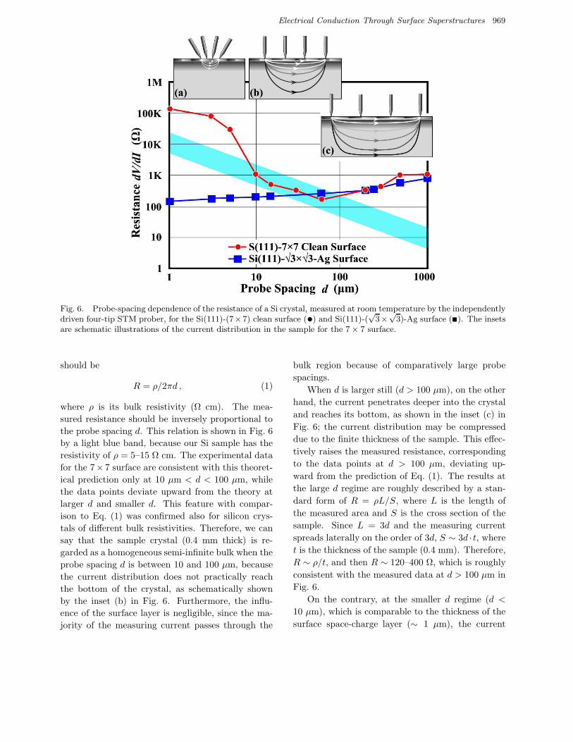
Electrical Conduction Through Surface Superstructures 969
Fig. 6. Probe-spacing dependence of the resistance of a Si crystal, measured at room temperature by the independentlydriven four-tip STM prober, for the Si(111)-(7×7) clean surface (•) and Si(111)-(
√3×
√3)-Ag surface (). The insets
are schematic illustrations of the current distribution in the sample for the 7 × 7 surface.
should be
R = ρ/2πd , (1)
where ρ is its bulk resistivity (Ω cm). The mea-
sured resistance should be inversely proportional to
the probe spacing d. This relation is shown in Fig. 6
by a light blue band, because our Si sample has the
resistivity of ρ = 5–15 Ω cm. The experimental data
for the 7× 7 surface are consistent with this theoret-
ical prediction only at 10 µm < d < 100 µm, while
the data points deviate upward from the theory at
larger d and smaller d. This feature with compar-
ison to Eq. (1) was confirmed also for silicon crys-
tals of different bulk resistivities. Therefore, we can
say that the sample crystal (0.4 mm thick) is re-
garded as a homogeneous semi-infinite bulk when the
probe spacing d is between 10 and 100 µm, because
the current distribution does not practically reach
the bottom of the crystal, as schematically shown
by the inset (b) in Fig. 6. Furthermore, the influ-
ence of the surface layer is negligible, since the ma-
jority of the measuring current passes through the
bulk region because of comparatively large probe
spacings.
When d is larger still (d > 100 µm), on the other
hand, the current penetrates deeper into the crystal
and reaches its bottom, as shown in the inset (c) in
Fig. 6; the current distribution may be compressed
due to the finite thickness of the sample. This effec-
tively raises the measured resistance, corresponding
to the data points at d > 100 µm, deviating up-
ward from the prediction of Eq. (1). The results at
the large d regime are roughly described by a stan-
dard form of R = ρL/S, where L is the length of
the measured area and S is the cross section of the
sample. Since L = 3d and the measuring current
spreads laterally on the order of 3d, S ∼ 3d · t, where
t is the thickness of the sample (0.4 mm). Therefore,
R ∼ ρ/t, and then R ∼ 120–400 Ω, which is roughly
consistent with the measured data at d > 100 µm in
Fig. 6.
On the contrary, at the smaller d regime (d <
10 µm), which is comparable to the thickness of the
surface space-charge layer (∼ 1 µm), the current
970 S. Hasegawa et al.
mainly flows near the surface, as shown in the inset
(a); the penetration depth of the current distribu-
tion in the sample is similar to the probe spacing in
the usual cases. Therefore, the data points in Fig. 6
indicate that the resistance at the surface region is
larger than that of the inner bulk, because the data
at d < 10 µm deviate upward from the light blue
band. This conclusion is reasonable when one re-
calls the fact that the surface space-charge layer be-
neath the clean 7 × 7 surface is always a depletion
layer, irrespective of the bulk doping concentration
and type. This is because the Fermi level at the sur-
face is strongly pinned by the dangling-bond state
located at the middle of the band gap.22,23 Thus the
surface region has a higher resistance for the 7 × 7
surface compared with the inner bulk region.
On the other hand, the d dependence of resistance
for the (√
3 ×√
3)-Ag surface does not fit Eq. (1)
at all. According to Ohm’s law in classical electro-
magnetism, when the resistance of an infinite two-
dimensional sheet is measured by a linear four-point
probe of probe spacing d, the measured resistance R
is written as
R = (ln 2/2π) · RS , (2)
where RS is the sheet resistance (Ω). This means
that the measured resistance should be constant,
independent of the probe spacing d. The experi-
mental data points for the (√
3 ×√
3)-Ag surface
in Fig. 6 roughly follow this tendency, rather than
Eq. (1). As described in detail in the next section,
the (√
3×√
3)-Ag surface has a two-dimensional free-
electron like surface-state band which is metallic and
conductive, and furthermore its surface space-charge
layer is always a weak hole-accumulation layer. This
is why the surface region has a much higher con-
ductivity than in the bulk.24 The contribution from
the surface-state band dominates the measured con-
ductance, as revealed in the next section. There-
fore, the conduction is two-dimensional, rather than
three-dimensional.
In this way, by changing the probe spacing from
macroscopic distances to microscopic ones, one can
switch the conductivity measurement from the bulk-
sensitive mode to a surface-sensitive one, so that one
can clearly distinguish between 2D conduction and
3D conduction.
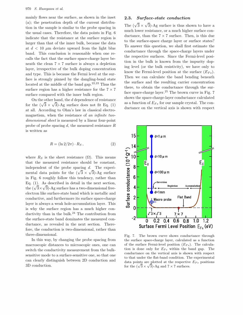
2.3. Surface-state conduction
The (√
3 ×√
3)-Ag surface is thus shown to have a
much lower resistance, or a much higher surface con-
ductance, than the 7 × 7 surface. Then, is this due
to the surface-space charge layer or surface states?
To answer this question, we shall first estimate the
conductance through the space-charge layers under
the respective surfaces. Since the Fermi-level posi-
tion in the bulk is known from the impurity dop-
ing level (or the bulk resistivity), we have only to
know the Fermi-level position at the surface (EFs).
Then we can calculate the band bending beneath
the surface and the resulting carrier concentration
there, to obtain the conductance through the sur-
face space-charge layer.25 The brown curve in Fig. 7
shows the space-charge-layer conductance calculated
as a function of EFs for our sample crystal. The con-
ductance on the vertical axis is shown with respect
Fig. 7. The brown curve shows conductance throughthe surface space-charge layer, calculated as a functionof the surface Fermi-level position (EFs). The calcula-tion is done only for EFs within the band gap. Theconductance on the vertical axis is shown with respectto that under the flat-band condition. The experimentaldata points are plotted at the respective EFs positionsfor the (
√3 ×
√3)-Ag and 7 × 7 surfaces.
Electrical Conduction Through Surface Superstructures 971
to that under the flat-band condition (where EFs co-
incides with EF in the bulk, 0.75 eV above the bulk
valence-band maximum in this case). When EFs is
located around the middle of the bulk band gap, the
surface space-charge layer is a depletion layer where
the conductance is low. When EFs is near the bulk
conduction-band minimum EC (valence-band maxi-
mum EV ), the layer is an electron (hole) accumula-
tion layer where the conductance is increased due to
the excess carriers in the layer.
Fortunately, the EFs positions at the 7 × 7 and
(√
3×√
3)-Ag surfaces are already known from pho-
toemission spectroscopy measurements22–24 to be
0.63 eV and 0.1–0.2 eV above EV , respectively.
These do not depend on the bulk doping level, owing
to the Fermi-level pinning by metallic surface states.
From Fig. 7, then, one can estimate the conductance
through the surface space-charge layer below the re-
spective surfaces. Since the 7 × 7 surface is located
in the depletion region and the (√
3 ×√
3)-Ag is in
a weak hole-accumulation region, the latter surface
should have a higher conductance than the former
by about 5 × 10⁻⁵Ω−1/.
Since the calculated conductance is not absolute
values, but just a change from that under the flat-
band condition, we cannot make a straightforward
comparison between the calculated conductance and
the experimental data. Therefore, we next have
to assume that the measured conductance of the
7× 7 clean surface is the space-charge-layer conduc-
tance only; no surface-state conductance contributes.
Then the data point of the 7 × 7 surface is right
on the calculated curve at EFs = 0.63 eV above
EV , as shown in Fig. 7. Since, then, we can obtain
the difference in conductance between the 7× 7 and
(√
3×√
3)-surfaces from their measured conductance
in Fig. 6, we can plot the results at the EFs position
of the (√
3×√
3)-Ag surface. These are indicated by
the bold straight blue line with circles. As shown in
Fig. 6, the conductance changes in a wide range, de-
pending on the probe spacing. As the probe spacing
is reduced, the measured conductance significantly
deviates upward from the calculated curve in Fig. 7.
Especially for the probe spacing of 1 µm, the mea-
sured conductance is higher than the expected space-
charge-layer conductance by more than one order of
magnitude. Therefore, the high conductance of the
(√
3 ×√
3)-Ag surface is explained not only by the
space-charge-layer conductance, rather, the surface-
state conductance dominantly governs the measured
value.
If the assumption mentioned above about con-
ductance of the 7 × 7 surface is not true, i.e. if the
surface-state conductance largely contributes to the
measured conductance for the 7× 7 surface, its data
point should be located above the calculated curve in
Fig. 7. Then the data points for the (√
3 ×√
3)-Ag
surface also deviate further upward above the cal-
culated curve. This means again that the contribu-
tion from the surface-state conductance is larger still.
Therefore, the above assumption does not affect the
conclusion of the surface-state conductance of the
(√
3×√
3)-Ag surface; rather, it makes an underesti-
mate for the surface-state conductance. Since there
are reports that the surface-state conductance of the
7×7 surface is 10−6–10−8 Ω−1,16,17 the conductance
is lower than that of the (√
3 ×√
3)-Ag surface by
2–4 orders of magnitude, which is negligibly low. In
any cases, the conclusion about the (√
3 ×√
3)-Ag
surface is not affected by whether the surface-state
conductance contributes on the 7× 7 surface.
The surface-state conductance of the (√
3×√
3)-
Ag surface was already detected and confirmed with
the macroscopic four-point probe method by observ-
ing a conductance increase due to carrier doping into
the surface-state band.14 But the microscopic four-
point probe method described here has made it pos-
sible just by comparing the conductance values be-
tween the two surfaces. This is owing to its high
sensitivity in measurements of the surface-state elec-
trical conduction.4 In other words, the microscopic
four-point probe, whose probe spacing is comparable
to the thickness of the space-charge layer, is an ef-
fective tool for detecting and measuring the surface-
state conductance of the topmost atomic layers.
In spite of the continuous efforts to detect the
surface-state conductance since the 1970’s, unam-
biguous experimental detections have been lacking
for a long time.18 Therefore, the results described
above are significant in surface physics, which opens
up a new opportunity of study on the transport prop-
erty of surface electronic states.
For comparison, a data point obtained by a
macroscopic four-point probe (probe spacing of
about 10 mm) is plotted as an open blue circle in
Fig. 7.21 Since this point is located close to the cal-
culated curve for the surface-space-charge-layer con-
ductance, we cannot say within the experimental
972 S. Hasegawa et al.
errors that the data point deviates significantly from
the calculated curve. Therefore, we could not con-
clude the contribution of the surface-state conduc-
tance just by comparing the measured conductance
between the 7× 7 and (√
3×√
3)-Ag surfaces in the
case of the macro-four-point probe method.21 This
is because the macro-probe method does not enable
precise measurements of surface-state conductance
for lack of sufficient surface sensitivity; the bulk con-
ductance mainly contributes to the measured values.
In spite of these analyses, however, some read-
ers may think that this reasoning is not convinc-
ing. Since, according to Fig. 7, the (√
3 ×√
3)-Ag
surface has an extremely high surface-state conduc-
tance compared with the conductance through the
surface space-charge layer, one may claim that the
surface-state conductance should be detected even
by the macroscopic four-point probe method in spite
of its low surface sensitivity. And its measured value
should be the same as those obtained by the micro-
four-point probe method once the contribution from
the bulk conductance is subtracted. Why does the
measured surface conductance depend on the probe
spacing?
As described by Eq. (2), if the sample is regarded
as an infinite 2D and homogeneous resistive sheet,
the measured resistance should be constant, inde-
pendent of the probe spacing d. This is because the
carrier scattering centers are distributed densely and
homogeneously; in other words, the spacing among
the scattering centers is much smaller than the probe
spacing, so that RS should be regarded as constant
irrespective of the size of the measured area, or the
probe spacing d. The data points in Figs. 6 and 7
evidently contradict this prediction.
This may be because the carrier scattering at
surface defects is effectively different between in the
macroscopic measurement and in the microscopic
one. Let us take atomic steps on a surface as an
example; as shown in the next section, atomic steps
scatter carriers, and cause resistance, resulting in se-
rious influence on the conductance. Even if the av-
erage step–step separation is the same, the influence
of the step on resistance may depend on the degree
of wandering of steps in macroscopic measurements;
imagine that meandering steps may scatter the carri-
ers more frequently than arrays of straight steps. But
when the conductance is measured in microscopic re-
gions where the probe spacing is comparable to the
distance between adjacent steps (i.e. terrace width),
the steps should be regarded as straight in the mea-
sured area even if the steps are winding in the macro-
scopic scale. Therefore the effective carrier scattering
may be reduced. Thus the resulting sheet resistance
RS can change depending on the scale of the mea-
sured areas. The conductance measured in micro-
scopic regions should be an intrinsic value, due to
reduction of the influence of atomic steps and other
surface defects.
Next, let us estimate the mean free path L of
the surface-state carriers. Since, as mentioned in the
previous subsection, the surface state of (√
3 ×√
3)-
Ag has a nearly free-electron-like band in two dimen-
sions, the sheet conductance σSS (= 1/RS) is written
by the Boltzmann picture as
σSS = SF · e2L/2πh , (3)
where SF is the circumference of the Fermi disk
(SF = 2πkF , where kF is the Fermi wave number), h
is Planck’s constant and e is the elementary charge.
Since kF is already measured by angle-resolved pho-
toemission spectroscopy,14,26 kF = 0.15 ± 0.02 A−1,
SF can be calculated. On the other hand, from
the data at d = 1 µm in Fig. 7, the surface-state
conductance is σSS = 1.5 × 10⁻³ Ω−1/. Then,
by substituting these values into Eq. (3), we obtain
L = 25 ± 3 nm for our sample at room temperature
(RT). This value is smaller than typical step–step in-
terval and domain size (∼ 100 nm) by nearly an order
of magnitude, meaning that the surface-state carri-
ers are scattered dominantly by phonons and surface
defects other than atomic steps and domain bound-
aries. This means a diffusive conduction even within
single domains and terraces at RT. But, for the de-
tails of the carrier scattering mechanism, we have
to measure the temperature dependence of conduc-
tance in a wide temperature range, which we are now
preparing to do. The important point here is that
even when the surface-state carriers are scattered by
some irregularities, they are not necessarily scattered
into the bulk-state bands. The surface-state carriers
can continue to run through the surface states for
a distance much longer than the mean free path, so
that the probes of several-µm spacing can effectively
detect the surface-state conductance. The scatter-
ing rate of the surface-state carriers into the bulk
states depends on the relation between the bulk and
surface band structures. Because the surface-state
Electrical Conduction Through Surface Superstructures 973
band contributing to the electrical conduction is lo-
cated within the energy gap in the bulk-state bands
for the (√
3 ×√
3)-Ag case — in other words, be-
cause the surface state is energetically isolated from
the bulk states — the surface-state carrier should
have a longer lifetime.
Next, let us estimate the mobility µ of the
surface-state carriers. The mean free path L can be
written as L = τVF , where τ is the relaxation time
and VF is Fermi velocity. The mobility µ is written
as
µ = eτ/m∗ , (4)
where m∗ is the effective mass of surface-state car-
riers. Since we know m∗ and kF from the band
dispersion measured by angle-resolved photoemission
spectroscopy,14,26 m∗ = (0.29±0.05)me, where me is
free electron mass, we can calculate VF = hkF /m∗.
Then we can obtain τ , too. As a result, we obtain
µ = 250±50 cm2/V ·s. This value is lower than that
of conduction electrons in three-dimensional bands of
a Si bulk crystal, 1500 cm2/V · s, by nearly an or-
der of magnitude. This means that the surface-state
carriers are scattered by phonons and defects more
seriously than the carriers in bulk. It should also
be noted that the mobility obtained here is higher
than that previously obtained by the macro-four-
point probe method by an order of magnitude.14
This means, as mentioned above, that the influence
of carrier scattering by surface defects is effectively
reduced in microscopic measurements compared with
macroscopic measurements, resulting in a larger mo-
bility. If one can measure the conductivity of al-
most defect-free regions with further smaller probes,
the measured mobility will apparently be further
increased.
In the next section, we shall introduce another
type of microscopic four-point probe method and
their preliminary results that directly show the in-
fluence of atomic steps on the conductance.
3. Monolithic Micro-Four-Point
Probes
3.1. Device and apparatus
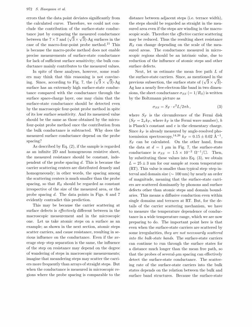
Figure 8(a) shows a scanning electron micrograph
(SEM) of a chip for a micro-four-point probe, which
is produced by using silicon microfabrication technol-
ogy at the Microelectronics Center of Denmark Tech-
nical University.4 The technique is similar to that
for producing cantilevers of atomic force microscopy.
The probes are now commercially available.27 One
can choose the probe spacing ranging from 2 µm to
100 µm, while probes of several-hundred-nm spacing
are under development. The substrate is an oxide-
covered silicon crystal, on which a metal layer is de-
posited to make conducting paths. The metal layer
covers the very end of four cantilevers so that they
can make direct contact with the sample surface.
The angle between the cantilever and the sample sur-
face is about 30, as shown by the inset in Fig. 8(a),
so that the cantilevers bend to make contact with
the sample easily for all of the four cantilevers even if
the tips of the four cantilevers are not strictly aligned
parallel to the sample surface.
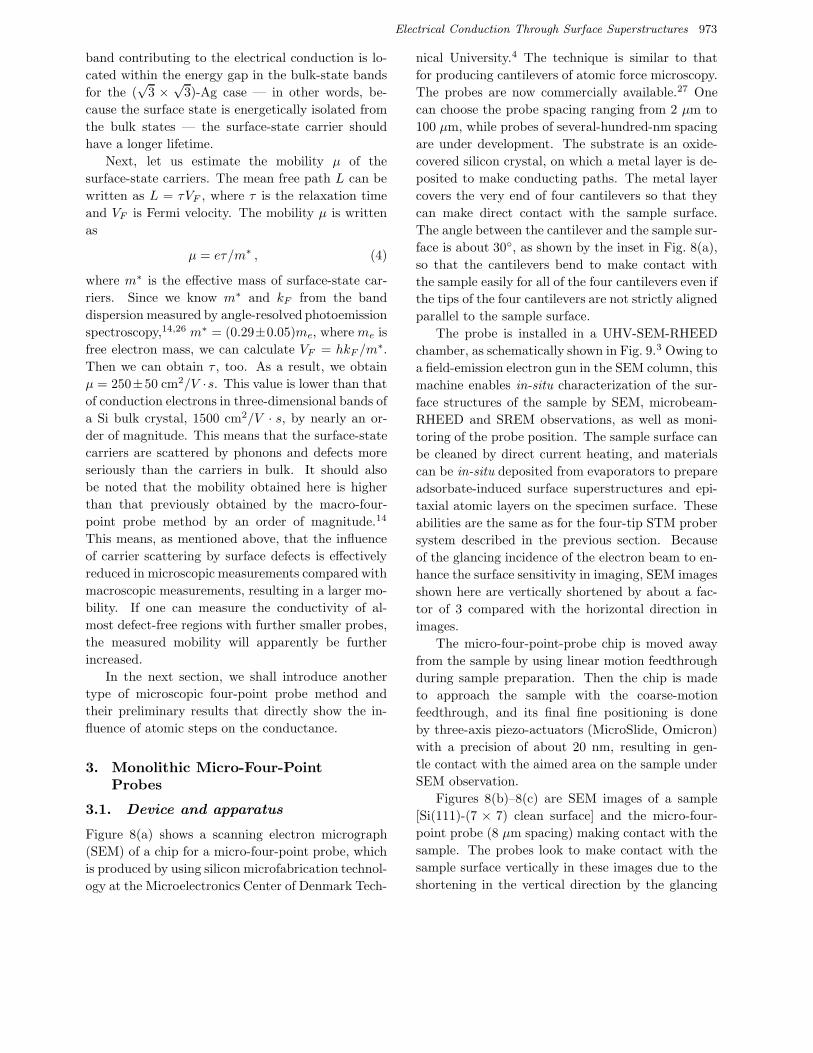
The probe is installed in a UHV-SEM-RHEED
chamber, as schematically shown in Fig. 9.3 Owing to
a field-emission electron gun in the SEM column, this
machine enables in-situ characterization of the sur-
face structures of the sample by SEM, microbeam-
RHEED and SREM observations, as well as moni-
toring of the probe position. The sample surface can
be cleaned by direct current heating, and materials
can be in-situ deposited from evaporators to prepare
adsorbate-induced surface superstructures and epi-
taxial atomic layers on the specimen surface. These
abilities are the same as for the four-tip STM prober
system described in the previous section. Because
of the glancing incidence of the electron beam to en-
hance the surface sensitivity in imaging, SEM images
shown here are vertically shortened by about a fac-
tor of 3 compared with the horizontal direction in
images.
The micro-four-point-probe chip is moved away
from the sample by using linear motion feedthrough
during sample preparation. Then the chip is made
to approach the sample with the coarse-motion
feedthrough, and its final fine positioning is done
by three-axis piezo-actuators (MicroSlide, Omicron)
with a precision of about 20 nm, resulting in gen-
tle contact with the aimed area on the sample under
SEM observation.
Figures 8(b)–8(c) are SEM images of a sample
[Si(111)-(7 × 7) clean surface] and the micro-four-
point probe (8 µm spacing) making contact with the
sample. The probes look to make contact with the
sample surface vertically in these images due to the
shortening in the vertical direction by the glancing
974 S. Hasegawa et al.
Fig. 8. Micro-four-point probe. (a) SEM image of the chip. The inset shows a schematic side view of the probe makingcontact with a sample surface. (b), (c) Glancing-incidence SEM images of a micro-four-point probe (probe spacing8 µm), making contact with a sample [Si(111)-(7 × 7) clean surface] in UHV during the measurement of conductance.The probe is shifted laterally from (b) to (c) by about 5 µm using piezoactuators for fine positioning.
Electrical Conduction Through Surface Superstructures 975
Fig. 9. Schematic of a UHV-SEM-RHEED system, combined with the micro-four-point probe system.
incidence of the electron beam; the probes actually
contact in a way described in the inset of Fig. 8(a).
The probe is shifted laterally by about 5 µm in
Fig. 8(c) from the position in Fig. 8(b). Thus, the lo-
cal conductance of the aimed areas can be measured
by fine positioning of the probe with the aid of in-
situ SEM. Compared with the four-tip STM prober
described in the previous section, it is much easier
to bring the probes into contact with the sample,
though we cannot change the probe spacing. These
two methods are complementary to each other in this
sense.
3.2. Influence of atomic steps
On the usual (nominally) flat (111) surface of a Si
crystal, atomic steps distribute regularly with a step–
step distance of 0.1–1 µm (regular-step surfaces) due
to slight misorientation in cutting the crystal. There-
fore, to measure the step influence by micro-four-
point probes of several-µm probe spacing (Fig. 8),
step-free regions (terraces) should be made wider
than the probe spacing by using the phenomenon
of step bunching. Then the probes enable the con-
ductance measurements at terrace areas of almost
step-free or step-bunch areas with hundreds of steps
accumulated, so that the influence of atomic steps
on conductance can be extracted by comparing the
data between such regions.
Fortunately, a method to control the step con-
figuration for obtaining wide terraces has already
been developed.28 As shown in Fig. 10(a), ar-
rays of small holes are made on a nominally flat
(but actually vicinal) Si(111) crystal surface using
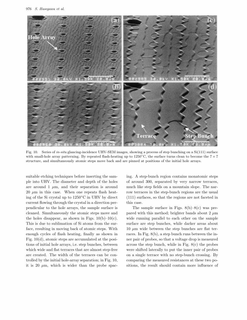
976 S. Hasegawa et al.
Fig. 10. Series of in-situ glancing-incidence UHV-SEM images, showing a process of step bunching on a Si(111) surfacewith small-hole array patterning. By repeated flash-heating up to 1250C, the surface turns clean to become the 7× 7structure, and simultaneously atomic steps move back and are pinned at positions of the initial hole arrays.
suitable etching techniques before inserting the sam-
ple into UHV. The diameter and depth of the holes
are around 1 µm, and their separation is around
20 µm in this case. When one repeats flash heat-
ing of the Si crystal up to 1250C in UHV by direct
current flowing through the crystal in a direction per-
pendicular to the hole arrays, the sample surface is
cleaned. Simultaneously the atomic steps move and
the holes disappear, as shown in Figs. 10(b)–10(c).
This is due to sublimation of Si atoms from the sur-
face, resulting in moving back of atomic steps. With
enough cycles of flash heating, finally as shown in
Fig. 10(d), atomic steps are accumulated at the posi-
tions of initial hole arrays, i.e. step bunches, between
which wide and flat terraces that are almost step-free
are created. The width of the terraces can be con-
trolled by the initial hole-array separation; in Fig. 10,
it is 20 µm, which is wider than the probe spac-
ing. A step-bunch region contains monatomic steps
of around 300, separated by very narrow terraces,
much like step fields on a mountain slope. The nar-
row terraces in the step-bunch regions are the usual
(111) surfaces, so that the regions are not faceted in
this case.
The sample surface in Figs. 8(b)–8(c) was pre-
pared with this method; brighter bands about 2 µm
wide running parallel to each other on the sample
surface are step bunches, while darker areas about
10 µm wide between the step bunches are flat ter-
races. In Fig. 8(b), a step bunch runs between the in-
ner pair of probes, so that a voltage drop is measured
across the step bunch, while in Fig. 8(c) the probes
were shifted laterally to put the inner pair of probes
on a single terrace with no step-bunch crossing. By
comparing the measured resistances at these two po-
sitions, the result should contain more influence of
Electrical Conduction Through Surface Superstructures 977
Fig. 11. Series of in-situ glancing-incidence UHV-SEM images during Ag deposition on a step-bunched Si(111)-(7×7)clean surface kept at 450C. With increasing Ag coverage, the brighter thin domains [(
√3×
√3)-Ag structure] appear
at monatomic step edges and expand, while the darker domains (7 × 7 clean structure) shrink [(b)–(d)]. Finally, thesurface is wholly covered by the brighter domains homogeneously in (e). (c′) and (d′) are magnified images, showingthat narrow terraces within step-bunch regions also change the structure. So the step bunches can be simply regardedas arrays of hundreds of monatomic steps. By comparing (a) with (e), it is noticed that the whole morphology of thesurface does not change during the structure conversion from 7 × 7 to (
√3 ×
√3)-Ag.
steps in (b) than in (c). In this way, the micro-four-
point probe enables the conductance measurements
of selected microscopic areas by precise positioning.
Figure 11 shows in-situ observations of SEM dur-
ing Ag deposition on such a step-bunched Si(111)-
(7 × 7) clean surface [Fig. 11(a)] kept at 450C.20
Bright thin lines begin to appear at the initial stage
of deposition, as shown in Fig. 11(b). The deposited
Ag atoms migrate on the surface at 450C, and are
then captured by atomic steps, where the 7×7 struc-
ture converts into the (√
3 ×√
3)-Ag structure. The
bright thin areas are the domains of the (√
3×√
3)-
Ag structure thus formed along steps, while darker
areas are domains of the clean 7× 7 structure. This
image shows that the terrace areas about 10 µm
wide are not completely step-free; rather, several
monatomic steps run across the wide terraces. But
this is a much lower step density compared with the
step-bunch areas where more than 100 steps are ac-
cumulated.
With increase of Ag coverage, the brighter areas
spread as seen in Figs. 11(c) and 11(c′), and simul-
taneously the (√
3×√
3)-Ag domains appear on ter-
races as well as near step edges, as in Figs. 11(d)
and 11(d′). Finally, with deposition of 1 ML of Ag,
the terraces and step bunches are wholly covered by
the brighter domains, as shown in Fig. 11(e). By
comparing Fig. 11(a) with Fig. 11(e), the surface
morphology of terrace–step-bunch structure is not
changed by the structure conversion from the 7 × 7
to (√
3 ×√
3)-Ag. The narrow terraces in the step-
bunch area have the same 7 × 7 and (√
3 ×√
3)-Ag
structures as on the wide terraces in (a) and (e),
respectively.
Figures 12(a) and 12(b) show “line profiles” of
resistance measured with the micro-four-point probe
(probe spacing d = 8 µm) by shifting it along a line
across step bunches on such step-bunched Si(111)-
(7 × 7) clean and (√
3 ×√
3)-Ag surfaces at RT, re-
spectively. The horizontal axis shows the position
of the probe on the line; the data points are plotted
at the position of the center of the micro-four-point
probe. The surface morphology observed by SEM
is schematically shown at the bottom of each graph;
the vertical scale is exaggerated. These results show
that the resistance changes drastically from place to
place. As expected, when the inner pair of probe
cross over a step bunch as shown in Fig. 8(b) (such
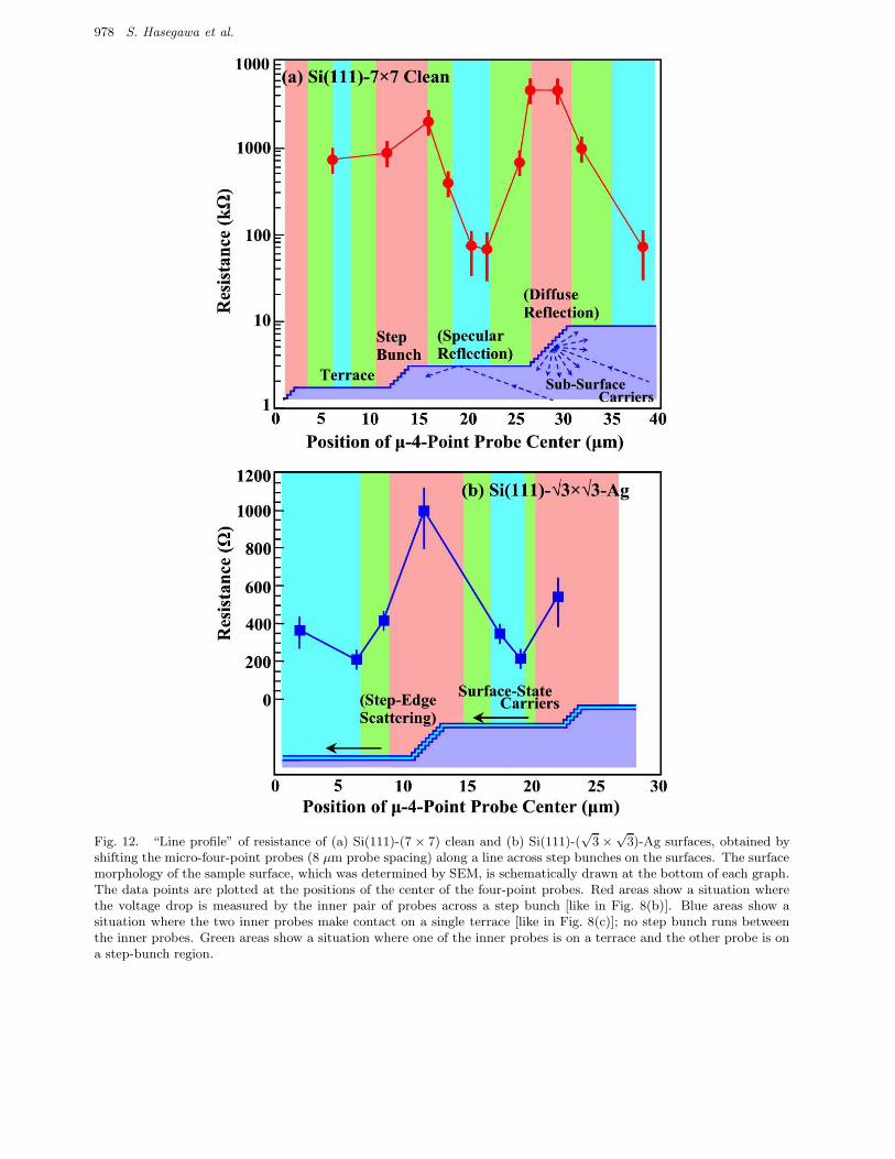
978 S. Hasegawa et al.
Fig. 12. “Line profile” of resistance of (a) Si(111)-(7 × 7) clean and (b) Si(111)-(√
3 ×√
3)-Ag surfaces, obtained byshifting the micro-four-point probes (8 µm probe spacing) along a line across step bunches on the surfaces. The surfacemorphology of the sample surface, which was determined by SEM, is schematically drawn at the bottom of each graph.The data points are plotted at the positions of the center of the four-point probes. Red areas show a situation wherethe voltage drop is measured by the inner pair of probes across a step bunch [like in Fig. 8(b)]. Blue areas show asituation where the two inner probes make contact on a single terrace [like in Fig. 8(c)]; no step bunch runs betweenthe inner probes. Green areas show a situation where one of the inner probes is on a terrace and the other probe is ona step-bunch region.
Electrical Conduction Through Surface Superstructures 979
a situation occurs at red areas in Fig. 12), the mea-
sured resistance is higher. When the inner pair of
probes make contact on the same terrace as shown in
Fig. 8(c) without crossing a step bunch (such a situa-
tion occurs at blue areas in Fig. 12), lower resistance
values are obtained. The 7 × 7 and (√
3 ×√
3)-Ag
surfaces show qualitatively the same results, but they
are quite different in magnitude of change.
An important issue should be commented on
here. In general, the four-point probe method works
only for homogeneous samples both in the surface-
parallel direction and in the depth direction. But the
present sample is not the case; the resistance at the
step-bunch areas is higher than that on the terraces.
So the measured resistances in Fig. 12 are not the
true values of the respective areas. We need a kind
of “deconvolution” from the measured data to obtain
the true values. Such a calculation will be published
elsewhere.29 But we can do qualitative discussions
from the raw data.
Since for the (√
3×√
3)-Ag surface, as described
in the previous section, the conductance is domi-
nated by the surface state, the result in Fig. 12(b)
means that the surface-state conduction is actually
interrupted at step edges. This is very reasonable
when one recalls STM pictures of so-called electron
standing waves near step edges on this surface di-
rectly observed by low-temperature STM,30 which
is nothing but the direct view of carrier scattering
at steps. Figure 12 shows the first direct measure-
ment of resistance caused by such step-edge scatter-
ing, from which we will be able to deduce the resis-
tance due to a single monatomic step and transmis-
sion (and reflection) coefficient of the electron wave
function of electrons there.
At this moment, we cannot directly detect the
influence of a single atomic step on the conductance.
It is still unclear whether the influence of a step
bunch can be regarded as a simple multiple of the
influence of a single atomic step. It may depend on
whether the transport is diffusive or ballistic at the
step-bunch regions. Strain fields, furthermore, are
created in the step-bunch regions due to the narrow
step–step distance, which may cause additional in-
fluence on the conductivity.
As shown in the previous section, the conduc-
tance of the 7 × 7 surface is lower than that of
the (√
3 ×√
3)-Ag surface by more than two orders
of magnitude, which is reasonable when one recalls
the reports about the surface-state conductance of
the 7 × 7 surface,16,17 giving it as small as 10−6–
10−8 Ω−1. The surface-state electrical conduction, if
any, is interrupted by steps in the same way as on
the (√
3×√
3)-Ag surface. The surface-space-charge-
layer conductance, which is also low because of the
depletion condition beneath the (7×7)-reconstructed
layer, is also influenced by the step bunches. The car-
riers flowing through the surface space-charge layer
should be perturbed by the step bunches on the
surface. This is because, according to the classi-
cal view of Fuchs–Sondheimer about carrier scatter-
ing at surfaces.31,32 the carriers are scattered diffu-
sively at the step bunch areas because of the surface
roughness, as illustrated at the bottom of Fig. 12(a),
while the carriers are reflected specularly at flat ter-
races. The diffusive scattering causes additional re-
sistance, while the specular reflection does not. Al-
ternatively, excess charges accumulated in electronic
states characteristic of the step edges may locally
disturb the band bending just below the step-bunch
regions, resulting in carrier scattering in the surface
space-charge layer. In this way, a higher resistance
is most likely to be detected across the step bunches
not only for the surface-state carriers but also for
the carriers flowing through the surface space-charge
layer.
Although the surface states are interrupted
at step edges, the surface-state carriers can pass
through the step edges with some probability, pen-
etrating into the surface states on the adjacent ter-
races. The transmission probability at the step edges
is less than 100%, but not zero. If the surface-state
electrons have extended wave functions like for the
(√
3 ×√
3)-Ag structure, the transmission probabil-
ity may be higher because of a larger overlap of wave
functions with that on the neighboring terraces. On
the contrary, the transmission probability may be
lower for surface states having a localized nature like
that of the 7 × 7 surface, because of the negligible
overlap of the wave function with that of the adjacent
terraces. So the influence of steps on the surface-
state conductance may be more significant for the
latter case. Actually, the resistance increases by two
orders of magnitude at step bunch regions for the
7×7 surface [Fig. 12(a)], while it increases by only a
factor of 4 for the (√
3×√
3)-Ag surface [Fig. 12(b)].
Such an intuitive expectation should be confirmed by
theoretical estimates.
980 S. Hasegawa et al.
4. Concluding Remarks
The microscopic four-point probe methods described
here are unique and powerful tools in surface sci-
ence, especially for studying surface transport, and
are expected to be increasingly important, because
the electrical conduction through one or two atomic
layers on surfaces may play essential roles in
nanometer-scale science and technology. The reader
may see the usefulness from the preliminary results
described here. Of course, the probes can be ap-
plied not only for the study of surface transport,
but also for transport properties of microscopic and
nanometer-scale objects. The probes will be used
under various conditions, such as at low and high
temperatures, under magnetic field, and under illu-
minations. We have already constructed a system
for the micro-four-point probe measurements at tem-
peratures down to 10 K in UHV. The results will be
reported elsewhere.
An important issue to be discussed about the
four-point probe method is the contact points be-
tween the probe and the sample surface. Although,
as mentioned in Sec. 1, the contact resistance is
virtually eliminated in the four-point probe mea-
surements, the contact conditions may influence the
measurement results, especially for the microscopic
probes. Since the contacts are direct ones, the atomic
arrangements at the very points of contact may be
destroyed. Then, the electronic structures, including
band bending, can change very close to the probe
contacts. Such distorted regions spread on the or-
der of Debye lengths. Therefore, when the probe
spacing is comparable to the Debye lengths, we will
have to take into account this effect. To avoid this
type of disturbance, the probe contacts should be
tunnel contacts, especially for nanometer-scale four-
point probes.
Acknowledgments
This work was done under a Grant-in-Aid from the
Ministry of Education, Science, Culture, and Sports
of Japan, including the International Collaboration
Program. The four-tip STM prober was constructed
during the Core Research for Evolutional Science
and Technology of the Japan Science and Technology
Corporation.
References
1. For a review, see: S. Hasegawa, X. Tong, S. Takeda,N. Sato and T. Nagao, Prog. Surf. Sci. 60, 89 (1999).
2. S. Hasegawa, J. Phys.: Cond. Matter 12, R463(2000).
3. I. Shiraki et al., Surf. Rev. Lett. 7, 533 (2000).4. C. L. Petersen et al., Appl. Phys. Lett. 77, 3782
(2000).5. I. Shiraki et al., Surf. Sci. 493, 643 (2001).6. S. Hasegawa, I. Shiraki, F. Tanabe and R. Hobara,
Current Appl. Phys. 2, 465 (2002).7. S. Hasegawa, I. Shiraki, T. Tanikawa, C. L. Petersen,
T. M. Hansen, P. Boggild and F. Grey, J. Phys.:
Cond. Matter 14, 8379 (2002).8. O. Pfennigstorf, A. Petkova, H. L. Guenter and M.
Henzler, Phys. Rev. B65, 045412 (2002).9. M. Henzler, T. Luer and J. Heitmann, Phys. Rev.
B59, 2383 (1999).10. M. Jalochowski, M. Hoffman and E. Bauer, Phys.
Rev. Lett. 76, 4227 (1996).11. M. Jalochowski, Prog. Surf. Sci. 48, 287 (1995).12. K. R. Kimberlin and M. C. Tringides, J. Vac. Sci.
Technol. A13, 462 (1995).13. L. Gavioli, K. R. Kimberlin, M. C. Tringides, J. F.
Wendelken and Z. Zhang, Phys. Rev. Lett. 82, 129(1999).
14. Y. Nakajima et al., Phys. Rev. B56, 6782 (1997);Phys. Rev. B54, 14134 (1996).
15. K. Yoo and H. H. Weitering, Phys. Rev. B65, 115424(2002); Phys. Rev. Lett. 87, 026802 (2001).
16. S. Heike et al., Phys. Rev. Lett. 81, 890 (1998).17. Y. Hasegawa et al., Surf. Sci. 358, 32 (1996).18. M. Henzler, in Surface Physics of Materials I, ed. J.
M. Blakely (Academic, New York, 1975), p. 241.19. P. Boggild et al., Rev. Sci. Instrum. 71, 2781 (2000),
Adv. Mater. 12, 947 (2000).20. For a review, see: S. Hasegawa et al., Jpn. J. Appl.
Phys. 39, 3815 (2000).21. C.-S. Jiang, S. Hasegawa and S. Ino, Phys. Rev. B54,
10389 (1996).22. F. J. Himpsel, G. Hollinger and R. A. Pollak, Phys.
Rev. B28, 7014 (1983).23. J. Viernow et al., Phys. Rev. B57, 2321 (1998).24. S. Hasegawa et al., Surf. Sci. 386, 322 (1997).25. For fundamentals of semiconductor surfaces, see e.g:
W. Moench, Semiconductor Surfaces and Interfaces
(Springer, Berlin, 1995).26. X. Tong et al., Phys. Rev. B57, 9015 (1998).27. Visit http://www.capres.com28. T. Ogino, Surf. Sci. 386, 137 (1997).29. T. M. Hansen et al., J. Appl. Phys., submitted.30. N. Sato et al., Phys. Rev. B59, 2035 (1999).31. E. H. Sondheimer, Adv. Phys. 1, 1 (1952).32. K. Fuchs, Proc. Cambridge Philos. Soc. 34, 100
(1938).