Embed Size (px)
Citation preview
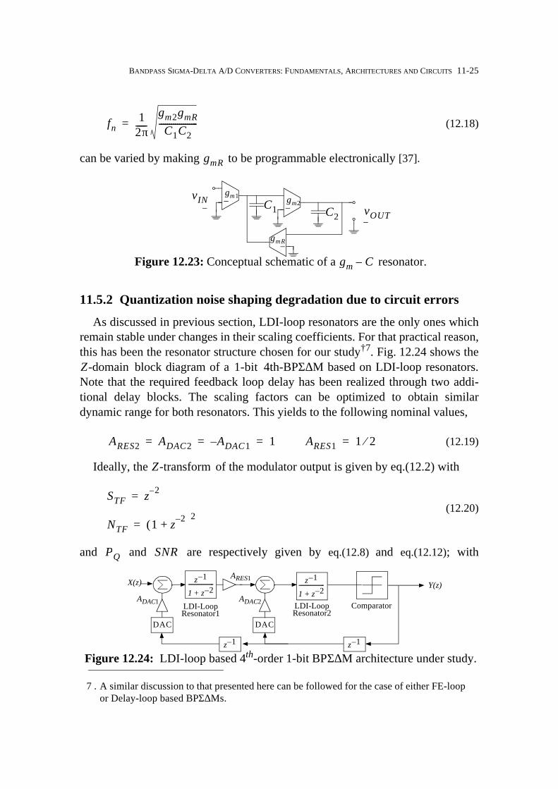
BANDPASS SIGMA-DELTA A/D CONVERTERS: FUNDAMENTALS, ARCHITECTURES AND CIRCUITS 11-1
Chapter 11
Bandpass Sigma-Delta A/D Converters:Fundamentals, Architectures and Circuits J. M. de la Rosa, B. Pérez-Verdú, Rocío del Río,
Fernando Medeiro and A. Rodríguez-Vázquez
11.1 INTRODUCTION
In last years we have witnessed a growth of the wireless communication marketas never before, introducing in our daily live a great number of digital portablegadgets such as cellular phones, digital radio receivers, Global Positioning Sys-tem (GPS) handheld units, Personal Digital Assistants (PDAs), etc. It is expectedthat this evolution will continue to do so in the first decade of this century, withthe proliferation of new technologies and applications such as Bluetooth, Soft-ware-Defined Radios (SDRs), Wireless Local Area Networks (WLANs), etc.
The wireless revolution has been partially prompted by the ‘vertiginous’ scal-ing-down of microelectronic technologies, which has exponentially increased thecapabilities of digital VLSI circuits, making it possible the integration of entirecommunication systems on the same silicon substrate. Together with reducedpriced, size and power consumption, the so-called Systems-on-Chips (SoCs) tendto realize more and more functions by a Digital Signal Processor (DSP), thusfacilitating the programmability and adaptability of these functions to many dif-ferent radio interface standards [1] − preferably reconfigurable with software[2][3]. For this purpose it would be desirable to place the analog-digital interfaceas closer to the antenna as possible.
In this scenario, Analog-to-Digital Converters (ADCs) based on BandPass Σ∆Modulators (BPΣ∆Ms) are very well suited for the implementation of the front-end of such digital wireless communication SoCs. One of the main advantages ofBPΣ∆Ms as compared to other architectures comes from the fact that they do notneed to digitize the whole Nyquist band (from DC to one half of the sampling fre-quency); instead they digitize just the signal band, thereby requiring much lesspower consumption to obtain similar dynamic range.
11-2 CMOS TELECOM DATA CONVERTERS
The principle of Σ∆ Modulation (Σ∆M) [4] is extended in BPΣ∆Ms to bandpasssignals, especially but not only, with a narrow bandwidth [5]. Thus, BPΣ∆Mshave much in common with their lowpass counterparts − whose properties havebeen covered in previous Chapters of this book. However, there are some issueswhich are peculiar to BPΣ∆-ADCs. This Chapter is devoted to the description ofthese issues. In Section 11.2, digital radio receivers are revised, pointing out thenecessity for an ADC at the IF location. Section 11.3 and Section 11.4 explain thebasic concepts and architectural issues of BPΣ∆-ADCs. The problems derivedfrom circuit implementation are treated in Section 11.5. Finally, Section 11.6summarizes the performance of state-of-the-art BPΣ∆-ADCs.
11.2 THE DIGITAL WIRELESS COMMUNICATIONS UNIVERSE
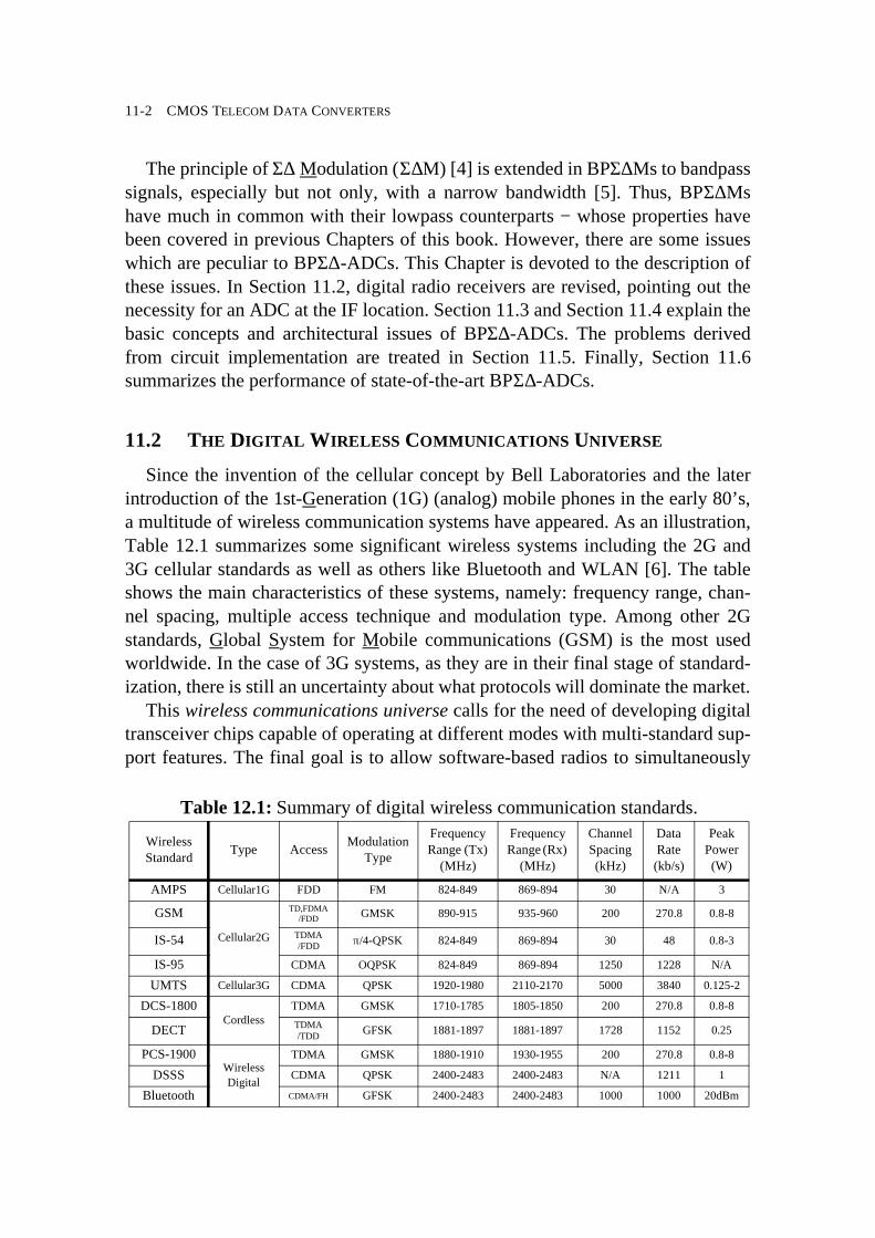
Since the invention of the cellular concept by Bell Laboratories and the laterintroduction of the 1st-Generation (1G) (analog) mobile phones in the early 80’s,a multitude of wireless communication systems have appeared. As an illustration,Table 12.1 summarizes some significant wireless systems including the 2G and3G cellular standards as well as others like Bluetooth and WLAN [6]. The tableshows the main characteristics of these systems, namely: frequency range, chan-nel spacing, multiple access technique and modulation type. Among other 2Gstandards, Global System for Mobile communications (GSM) is the most usedworldwide. In the case of 3G systems, as they are in their final stage of standard-ization, there is still an uncertainty about what protocols will dominate the market.
This wireless communications universe calls for the need of developing digitaltransceiver chips capable of operating at different modes with multi-standard sup-port features. The final goal is to allow software-based radios to simultaneously
Table 12.1: Summary of digital wireless communication standards.
Wireless Standard
Type AccessModulation
Type
Frequency Range (Tx)
(MHz)
Frequency Range (Rx)
(MHz)
Channel Spacing (kHz)
Data Rate (kb/s)
Peak Power (W)
AMPS Cellular1G FDD FM 824-849 869-894 30 N/A 3
GSM
Cellular2G
TD,FDMA/FDD GMSK 890-915 935-960 200 270.8 0.8-8
IS-54 TDMA/FDD π/4-QPSK 824-849 869-894 30 48 0.8-3
IS-95 CDMA OQPSK 824-849 869-894 1250 1228 N/A
UMTS Cellular3G CDMA QPSK 1920-1980 2110-2170 5000 3840 0.125-2
DCS-1800Cordless
TDMA GMSK 1710-1785 1805-1850 200 270.8 0.8-8
DECT TDMA/TDD GFSK 1881-1897 1881-1897 1728 1152 0.25
PCS-1900Wireless Digital
TDMA GMSK 1880-1910 1930-1955 200 270.8 0.8-8
DSSS CDMA QPSK 2400-2483 2400-2483 N/A 1211 1
Bluetooth CDMA/FH GFSK 2400-2483 2400-2483 1000 1000 20dBm
BANDPASS SIGMA-DELTA A/D CONVERTERS: FUNDAMENTALS, ARCHITECTURES AND CIRCUITS 11-3
carry voice, video and data, using a variety of telecommunication systems [3].
11.2.1 The ideal digital wireless transceiver
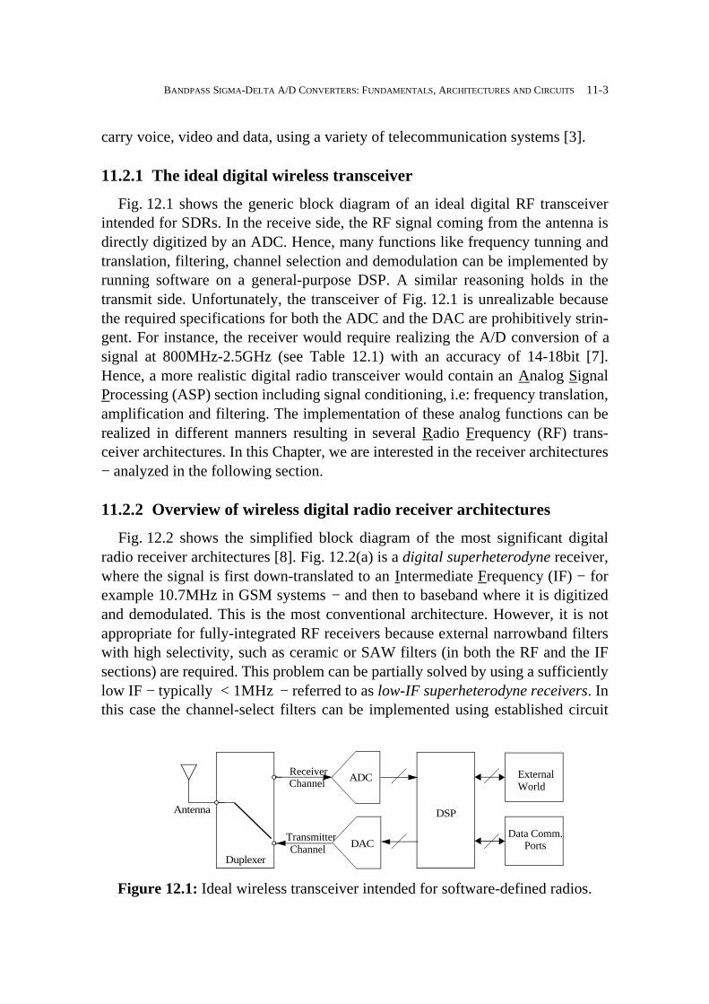
Fig. 12.1 shows the generic block diagram of an ideal digital RF transceiverintended for SDRs. In the receive side, the RF signal coming from the antenna isdirectly digitized by an ADC. Hence, many functions like frequency tunning andtranslation, filtering, channel selection and demodulation can be implemented byrunning software on a general-purpose DSP. A similar reasoning holds in thetransmit side. Unfortunately, the transceiver of Fig. 12.1 is unrealizable becausethe required specifications for both the ADC and the DAC are prohibitively strin-gent. For instance, the receiver would require realizing the A/D conversion of asignal at 800MHz-2.5GHz (see Table 12.1) with an accuracy of 14-18bit [7].Hence, a more realistic digital radio transceiver would contain an Analog SignalProcessing (ASP) section including signal conditioning, i.e: frequency translation,amplification and filtering. The implementation of these analog functions can berealized in different manners resulting in several Radio Frequency (RF) trans-ceiver architectures. In this Chapter, we are interested in the receiver architectures− analyzed in the following section.
11.2.2 Overview of wireless digital radio receiver architectures
Fig. 12.2 shows the simplified block diagram of the most significant digitalradio receiver architectures [8]. Fig. 12.2(a) is a digital superheterodyne receiver,where the signal is first down-translated to an Intermediate Frequency (IF) − forexample 10.7MHz in GSM systems − and then to baseband where it is digitizedand demodulated. This is the most conventional architecture. However, it is notappropriate for fully-integrated RF receivers because external narrowband filterswith high selectivity, such as ceramic or SAW filters (in both the RF and the IFsections) are required. This problem can be partially solved by using a sufficientlylow IF − typically − referred to as low-IF superheterodyne receivers. Inthis case the channel-select filters can be implemented using established circuit
Figure 12.1: Ideal wireless transceiver intended for software-defined radios.
Antenna
ADC
DSP
Duplexer
Receiver Channel
Transmitter Channel DAC
External World
Data Comm.Ports
1MHz<

11-4 CMOS TELECOM DATA CONVERTERS
techniques such as or Switched-Capacitor (SC). However, the use of alow IF imposes very demanding requirements for the Image-Reject (IR) filter†1.
In order to relax the IR filter requirements, an analog quadrature mixer can beused in both the RF and the IF sections [9]. As an illustration, Fig. 12.3(a) showsthe IF section of a superheterodyne receiver including a quadrature mixer. Note
1 . The problem of suppressing signals in the image band will be discussed later.
Figure 12.2: Digital RF receivers. (a) Superheterodyne. (b) Direct conversion. (c) IF conversion.
(a)
(b)
RF FilterLO1
Antenna
IF FilterLO2
IF Amp
RF Section IF Section Baseband Section
LowpassADC
DSP
RF Filter
Antenna LNA
RF Section Baseband Section
LowpassADC
DSP
IF Section
BandpassADC
DSP
(c)
LO1
LNA
IR Filter
RF FilterLO1
Antenna
RF Section
LNA
IR Filter
gm C–
Figure 12.3: Using quadrature mixers in: (a) Superheterodyne receivers. (b) IF-conversion receivers.
(b)(a)
LPF
LPF
Lowpass I data
Q data
IF Signal
LPF
LPF
π 2⁄
I data
Q data
IF Signal
ADCANALOG DIGITAL
ANALOG DIGITAL
2πfIFt( )cos2πfIFnTs( )cos 1 0 1 0 1 0 …, , , ,–, ,=
fIF fs 4⁄=Bandpass
ADC
LowpassADC
π 2⁄

BANDPASS SIGMA-DELTA A/D CONVERTERS: FUNDAMENTALS, ARCHITECTURES AND CIRCUITS 11-5
that two lowpass ADCs are needed to digitize the resulting In-phase (I) andQuadrature (Q) components. These quadrature signals are complex combined inorder to cancel the image power in the downconverted signal band. In practice,however, there is not a complete cancellation of the image due to gain and phasemismatch between quadrature paths in Fig. 12.3(a).
For that reason, other alternatives have been explored in last years to improvethe IR problem in low-IF superheterodyne receivers. One of them is based on theintegration of an IF quadrature mixer with a lowpass Σ∆M, usually referred to asIF-to-Baseband Σ∆Ms [10][11]. In these architectures, the mixer errors are shapedso that they are reduced in the desired band. In practical circuit realizations, the IRfeature is limited by I/Q path mismatches, which requires the use of additionalcompensation strategies like dynamic element matching algorithms [10].
The IR problem can be completely eliminated by using the receiver shown inFig. 12.2(b), known as direct conversion, zero-IF or homodyne receiver. In thisarchitecture, the RF signal is mixed-down directly to DC where is digitized. Thisapproach is more suited to integration than the superheterodyne because it elimi-nates the IF section. Hence, only off-chip RF filters are required since, as theimage and the desired signal are the same, the IR filter can be removed. However,the offset and flicker noise of the mixer are present in the middle of the signalband and can severely degrade the performance of this type of receivers.
Many of the problems arising in the above mentioned receiver architectures canbe eliminated using the IF-conversion receiver, shown in Fig. 12.2(c). In thisarchitecture the in-coming signal at the antenna is first mixed-down to IF where itis digitized. Thus, the signal is first translated to the digital domain by one ADC,referred to as bandpass or IF ADC, and then mixed to the baseband as shown inFig. 12.3(b). This is advantageous for several reasons. On the one hand, asquadrature mixing is done in the digital domain, the problems associated with theanalog mixer in the receiver shown in Fig. 12.3(a) are avoided [12]. Anotheradvantage of the IF-conversion receiver is that it allows channel-select filtering,gain control and demodulation to be handled in the digital domain [13][14]. Thisresults in robust RF receivers with a high degree of programmability, thus allow-ing a single software-controlled RF receiver to be employed for multi-standardreceivers [15].
11.2.3 IF A/D Conversion − Bandpass Σ∆ modulators
Digitization in IF-conversion receivers can be accomplished either with a wide-band Nyquist-rate ADC or a BPΣ∆-ADC. The use of the latter is the optimumsolution since the bandwidth of IF signals is typically much smaller than the car-rier frequency, and hence, reducing the quantization noise in the entire Nyquist
11-6 CMOS TELECOM DATA CONVERTERS
band becomes superfluous. Instead, by using BPΣ∆-ADCs the quantization noisepower is reduced only in a narrowband around the IF location, thus taking advan-tage of the higher oversampling ratio†2 and hence yielding to a high resolution.
BandPass Σ∆ Modulators (BPΣ∆Ms) extend the noise-shaping concept fromthe conventional LowPass Σ∆Ms (LPΣ∆Ms) − in which the quantization noise issuppressed around DC − to a more general case where the quantization noise isreduced in a narrow passband centred at an IF location [5][17]. Thus, the designand analysis of BPΣ∆Ms share much in common with LPΣ∆Ms [12].
The rest of the chapter is devoted to the study of BPΣ∆-ADCs, surveying thedifferent design issues, from architectures to circuit implementation.
11.3 BASIC CONCEPTS OF BANDPASS Σ∆ A/D CONVERTERS
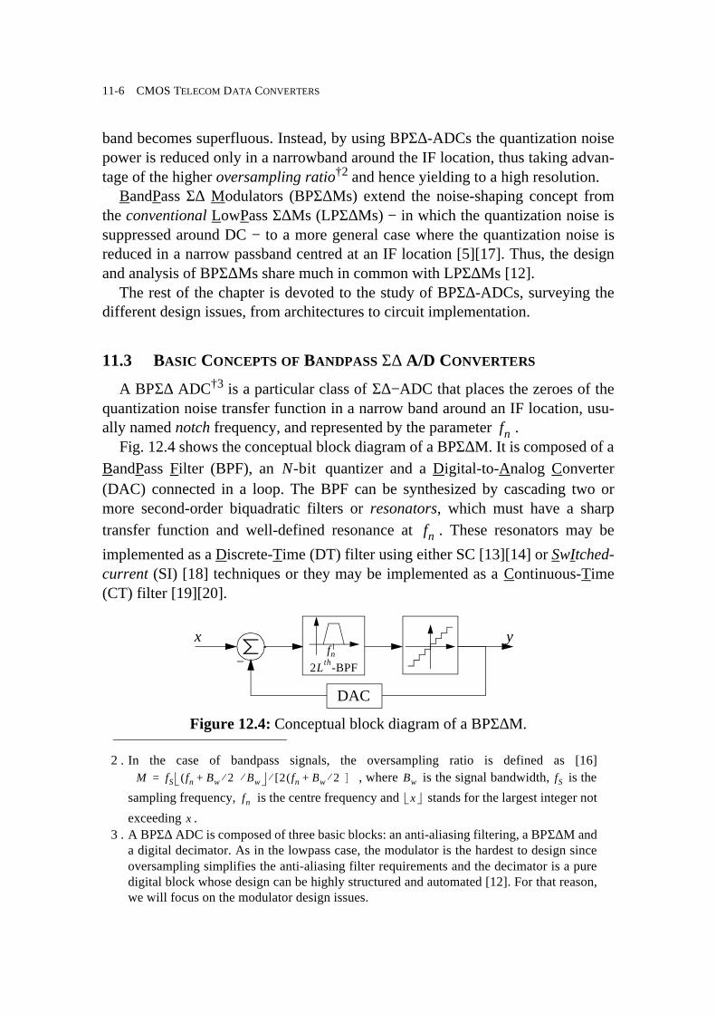
A BPΣ∆ ADC†3 is a particular class of Σ∆−ADC that places the zeroes of thequantization noise transfer function in a narrow band around an IF location, usu-ally named notch frequency, and represented by the parameter .
Fig. 12.4 shows the conceptual block diagram of a BPΣ∆M. It is composed of aBandPass Filter (BPF), an quantizer and a Digital-to-Analog Converter(DAC) connected in a loop. The BPF can be synthesized by cascading two ormore second-order biquadratic filters or resonators, which must have a sharptransfer function and well-defined resonance at . These resonators may be
implemented as a Discrete-Time (DT) filter using either SC [13][14] or SwItched-current (SI) [18] techniques or they may be implemented as a Continuous-Time(CT) filter [19][20].
2 . In the case of bandpass signals, the oversampling ratio is defined as [16], where is the signal bandwidth, is the
sampling frequency, is the centre frequency and stands for the largest integer not
exceeding .3 . A BPΣ∆ ADC is composed of three basic blocks: an anti-aliasing filtering, a BPΣ∆M and
a digital decimator. As in the lowpass case, the modulator is the hardest to design sinceoversampling simplifies the anti-aliasing filter requirements and the decimator is a puredigital block whose design can be highly structured and automated [12]. For that reason,we will focus on the modulator design issues.
M fS fn Bw 2⁄+( ) Bw⁄ 2 fn Bw 2⁄+( )[ ]⁄= Bw fS
fn x
x
fn
N-bit
fn
Figure 12.4: Conceptual block diagram of a BPΣ∆M.
+
−
x y
DAC
fn
2Lth-BPF

BANDPASS SIGMA-DELTA A/D CONVERTERS: FUNDAMENTALS, ARCHITECTURES AND CIRCUITS 11-7
Let us consider that the BPF is a filter composed of a cascade of
resonators with a DT†4 transfer function given by:
(12.1)
where and are the conjugate-complex poles of . Assuming that the
quantization error can be modelled as an additive, white noise source, the of the modulator output in Fig. 12.4 can be written as:
(12.2)
where the signal transfer function and the noise transfer function are respectively:
(12.3)
(12.4)
Note that has zeroes at and . In most practical
cases, and are placed in the unit circle, i.e, , with
being the sampling period. In some BPΣ∆Ms the value of can be either
digitally [21] or continuously [22] programmable, thus allowing to be changed
without changing . This is especially useful in radio applications, where the use
of a tunable BPΣ∆M eliminates the necessity of a channel-selection function inRF receivers.
Assuming that is synthesized in such a way that
(12.5)
yields:
4 . A similar discussion can be held for CT-BPΣ∆Ms. This class of modulators are inter-nally DT systems as will be discussed in Section 11.4.5.
2Lth-order L
HR z( )NR z( )
1 z 1– zn–( ) 1 z 1– zn∗–( )
--------------------------------------------------------=
zn zn∗ HR z( )
z-transform
Y z( ) STF z( )X z( ) NTF z( )Eq z( )+=
STF z( )NR z( )[ ]L
NR z( ) 1 z 1– zn–( ) 1 z 1– zn∗–( )+[ ]
L------------------------------------------------------------------------------------=
NTF z( )1 z 1– zn–( ) 1 z 1– zn∗–( )[ ]
L
NR z( ) 1 z 1– zn–( ) 1 z 1– zn∗–( )+[ ]
L------------------------------------------------------------------------------------=
NTF z( ) L z zn= z zn∗=
zn zn∗ zn j 2πfnTS( )[ ]exp=
TS fn
fn
fS
NR z( )
NR z( ) 1 z 1– zn–( ) 1 z 1– zn∗–( )+ 1=

11-8 CMOS TELECOM DATA CONVERTERS
(12.6)
and the Power Spectral Density (PSD) of the shaped quantization noise is:
(12.7)
where is the quantization step, defined as , with being
the full-scale range of the quantizer.The quantization noise in-band power can be calculated as follows:
(12.8)
where is the signal bandwidth and has been assumed. An important
conclusion is that, although the BPΣ∆M of Fig. 12.4 is a modulator,
the quantization noise is suppressed with bandstop filtering. In other
words, the quantization noise shaping of a BPΣ∆M is equal to that of
an LPΣ∆M. As an illustration, Fig. 12.5(a) plots several simulated out-put spectra of the modulator in Fig. 12.4 for , and different
values of . The input is a sinusoidal signal of a frequency close to and an
amplitude , with being the output level of the DAC. As
Fig. 12.5(a) shows, the output spectrum of the modulator can be seen as the sumof two components: the input signal spectrum (a vertical line) and the quantizationnoise spectrum. The form of the shaped quantization noise is like a valley with its
NTF z( ) 1 2 2πfnTS( )cos z 1–– z 2–+[ ]L
=
SQ f( ) ∆2
12fS---------- NTF f( ) 2 ∆2
12fS---------- 4 π f fn–( )TS[ ] π f fn+( )TS[ ]sinsin 2L= =
∆ ∆ XFS 2N 1–( )⁄≡ XFS
PQ 2SQ f( ) fdfn Bw 2⁄–
fn B+ w 2⁄
∫2πfnTS[ ]sin( )2Lπ2LXFS
2
12 2N 1–( )2
2L 1+( )M 2L 1+( )------------------------------------------------------------------------≅=
Bw Bw fn«
2Lth-order
Lth-order
2Lth-order
Lth-order
Figure 12.5: (a) Ideal output spectra of a 2Lth-order BPΣ∆M. (b) vs. .DR M(a) (b)
0 0.1 0.2 0.3 0.4 0.5-140
-120
-100
-80
-60
-40
-20
0
6th Order BP
4th Order BP
2nd Order BP
Rel
ativ
e M
agni
tude
(dB
)
Relative Frequency1 2 4 8 16 32 64 128 2560
20
40
60
80
100
120
DR
dB()
M
6th Order BP L 3=( )4th Order BP L 2=( )2nd Order BP L 1=( )
9dB/octave
15dB/octave
21dB/octave
N 1=fn fS 4⁄=
fn
Bw
N 1= fn fS 4⁄=
L fn
A AREF 2⁄= AREF

BANDPASS SIGMA-DELTA A/D CONVERTERS: FUNDAMENTALS, ARCHITECTURES AND CIRCUITS 11-9
minimum value at .
The Signal-to-Noise Ratio ( ) and the Dynamic Range ( ) for the modu-lator of Fig. 12.4, are given respectively by:
(12.9)
(12.10)
Note that for a BPΣ∆M, the quantization noise increases at a rate of
, which is equivalent to a LPΣ∆M. This isshown in Fig. 12.5(b) by plotting , computed from the spectra inFig. 12.5(a).
11.3.1 Signal passband location
In theory, the passband of a BPΣ∆M can be placed at any frequency from DCto . Thus, for a given input signal centre frequency, (the IF location in a
wireless receiver) and bandwidth, , the choice of the ratio is a trade-off
among sampling frequency (directly related to the speed of the whole system),anti-aliasing filter requirements, and oversampling ratio. As illustrated inFig. 12.6(a), the transition band, , of the anti-aliasing filter becomes sharper as
approaches . Thus, the lower the higher . However,
the use of low complicates the problem of suppressing image-band signals
when the RF signal is mixed down to an IF location. This is illustrated inFig. 12.6(b), where the incoming RF signal is centered at . Note that, an IR
filtering must be performed preceding the mixer to avoid image-band signals cen-tered at to corrupt the desired signal [1][8].
In order to cope with both IR and anti-aliasing filter requirements, must be
located at an intermediate location in the Nyquist band. An optimum solution tothis problem is to place at one-quarter of the sampling frequency. This notch
frequency location, in addition to relaxing the mentioned filter specifications,offers several advantages. First, the forward path loop (analog) filter realization
fn
SNR DR
SNR A2 2⁄PQ
-------------≡3 2N 1–( )
22L 1+( )M2L 1+
2π2L 2πfnTs[ ]sin( )2L-----------------------------------------------------------------2AXFS---------
2=
DRXFS 2⁄( )2
2PQ-----------------------≡
3 2N 1–( )2
2L 1+( )M2L 1+
2π2L 2πfnTs[ ]sin( )2L-----------------------------------------------------------------=
2Lth-order
2L 1+( ) 2( )log[ ]dB octave⁄ Lth-orderDR vs. M
fS 2⁄ fIF
Bw fn fS⁄
Btr
fn fS 2⁄ fn fIF=( ) Btrmax
fIF
fRF
fRF 2fIF–
fn
fn

11-10 CMOS TELECOM DATA CONVERTERS
can be relatively simplified. Secondly, it makes simpler the synthesis of bandpassarchitectures, which can be easily derived from lowpass prototypes with a simple
variable transformation (for instance ) as will be described in the nextsection. Last but not least, the design of the digital mixing to baseband (seeFig. 12.3(b)) is obviously simplified because the digital cosine and sine signalsare equal to the data series and , respectively.
In addition to the mentioned advantages, making also offers the
possibility of centering the IF signal at as demonstrated in [23] − the spec-
trum is symmetrical with respect to . This approach offers several advan-
tages. On the one hand, making the anti-aliasing filter requirements
are the same as for , but the IR filter specifications are relaxed. On the
other hand, it allows for either the clock rate to be reduced to one-third or process-ing signals to be three times higher in frequency. The only drawback is that theoversampling ratio is also reduced by a factor of three. For example, in the case ofa 4th-order BPΣ∆M, this means a loss of .
11.3.2 Decimation for bandpass Σ∆ ADCs
The decimator filter is the last stage of a Σ∆ ADC. This block realizes twooperations on the modulator output bit stream: filtering the out-of-band quantiza-tion noise and reducing the sampling rate to the Nyquist rate [12].
Fig. 12.7 illustrates the decimation process in BPΣ∆-ADCs. The modulator
Figure 12.6: Choice of the signal passband location. (a) Trade-off among anti-aliasing filter requirements and high values of . (b) Trade-off among IR filter
requirements and low values of .fIF
fIF
(b)
(a)fS 2⁄ fS
Bw
fn fS fn–fS 2⁄–f– S
Bw
f– nfS– fn+
IF Signal IF MirrorBtrAnti-aliasing Filter
Magnitude
fLOfLO fIF– fRF
RF Image RF Signal
Image-rejection Filter
Magnitude LO
fLO fRF fIF–=( )
f– LOf– LO fIF+f– RF
RF Signal Mirror
Image-rejection Filter
LOImage Mirror
Frequency
Frequency
z 1– z 2––→
1 0 1 0 …, ,–, ,( ) 0 1 0 1 …,–, , ,( )fn fS 4⁄=
3fS 4⁄
fS 2⁄
fIF 3fS 4⁄=
fIF fS 4⁄=
DR 3.7bit

BANDPASS SIGMA-DELTA A/D CONVERTERS: FUNDAMENTALS, ARCHITECTURES AND CIRCUITS 11-11
output, , is first filtered by a bandpass filter with a digital cut-off frequency at. This filter removes all out-of-band components in order to
avoid aliasing in the subsequent compressor stage. Thus, the band-limited signalresulting from the filtering, , is downsampled by discarding out of every
samples to produce the decimated signal, , at the Nyquist rate.
Note that the scheme of Fig. 12.7 requires a high-Q narrow-band BPF with ahigh passband center frequency. This yields an increase of cost, in terms of powerconsumption and silicon area, as compared to the lowpass case. This problem canbe avoided by using the scheme shown in Fig. 12.8, composed of a complexmixer and a complex lowpass filter [24]. The modulator output is mixed down tobaseband through the multiplication of . This scheme can be
notably simplified if because the multiplying signal is a sum of two
periodic data series containing and as illustrated in Fig. 12.8.Note that, as the inputs to the lowpass filters are zeros in alternate clock cycles,
the two lowpass filters can be simplified by only one multiplexed in time.
11.4 SYNTHESIS OF BANDPASS Σ∆ MODULATOR ARCHITECTURES
The basic structure of a BPΣ∆M is analogous to that of an LPΣ∆M except forthe type of loop filter. Thus, the operation of both types of Σ∆Ms is based on thesame strategy to attenuate the quantization noise. Hence, although most of thedesign art developed for LPΣ∆Ms can be used to develop BPΣ∆Ms, there aresome aspects of the modulator design which are peculiar to BPΣ∆Ms. This facthas motivated the development of several methods for synthesizing BPΣ∆Marchitectures. This section summarizes the most important of these methods.
Figure 12.7: Decimation process in BPΣ∆-ADCs.
Digital BP Filter Downsampler
Mfn
f
f f
fS 2⁄
Y f( )
H f( ) W f( )
fS 2⁄ fS 2⁄
Bw
fn
w
Bw
f
Yd f( )
Bw 2Bw
yBw fS 2M( )⁄=
w M 1–M yd
j2πfnnTS–( )exp
fn fS 4⁄=
0's 1's±

11-12 CMOS TELECOM DATA CONVERTERS
11.4.1 The lowpass-to-bandpass transformation method: LP-to-BP
As shown in Section 11.3, an LPΣ∆M and a BPΣ∆M,present identical figures of merit: and . Consequently, a simple way tosynthesize any BPΣ∆M architecture is to apply a Lowpass-to-Bandpass (LP-to-BP) transformation to an LPΣ∆M that meets a given specification. The LP-to-BPtransformation most extensively used in BPΣ∆M Integrated Circuits (ICs) is:
(12.11)
Applying the above transformation to the LPΣ∆M of Fig. 12.9(b),
the BPΣ∆M of the Fig. 12.9(a) is obtained. Assuming a linear model
Figure 12.8: Efficient decimator for BPΣ∆Ms.
Complex LP Filter + Downsampler
ej2πfnnTS–
y yd( )
fn
fS
4---=
1 0 1 0 …, ,–, ,
0 1 0 1 …,–, , ,
yMultiplexed Time LP Filter
I DATA
Q DATA
yd( )
I DATA
Q DATA+ Downsampler
Lth-order 2Lth-orderSNR DR
z 1– z 2––→
Lth-order
2Lth-order
Figure 12.9: (a) Block diagram of the BPΣ∆M derived by applying
to the LPΣ∆M shown in (b).
2Lth-order
z 1– z 2––→ Lth-order
z 1–
1 z 1––----------------
+
−
x y
DAC
gx1
gDAC1
z 1–
1 z 1––----------------
gDAC2
gx2
z 1–
1 z 1––----------------
gDACL
gxL
z– 2–
1 z 2–+----------------
+
−
x
DAC
gx1
gDAC1
z– 2–
1 z 2–+----------------
gDAC2
gx2
z– 2–
1 z 2–+----------------
gDACL
gxL
(b)
(a)
y

BANDPASS SIGMA-DELTA A/D CONVERTERS: FUNDAMENTALS, ARCHITECTURES AND CIRCUITS 11-13
for the quantizer, the of the BPΣ∆M output is given by:
(12.12)
As illustrated in Fig. 12.10, the zeroes of the are mapped from DC (in the
original LPΣ∆M) to (in the resulting BPΣ∆M), which corresponds to
in Fig. 12.10.
Note that, as a consequence of the transformation in eq.(12.11), the integratorsof the original LPΣ∆M become resonators in the resulting BPΣ∆M, which have
the transfer function in eq.(12.1) with and .
The shaped quantization noise power, , of the modulator in Fig. 12.9, can be
obtained by substituting in eq.(12.8), yielding to an identical expres-
sion to that of an LPΣ∆M. In an analogous way, the and the
are identical to that obtained in a LPΣ∆M [25].
In general, any , BPΣ∆M can be obtained by applying the
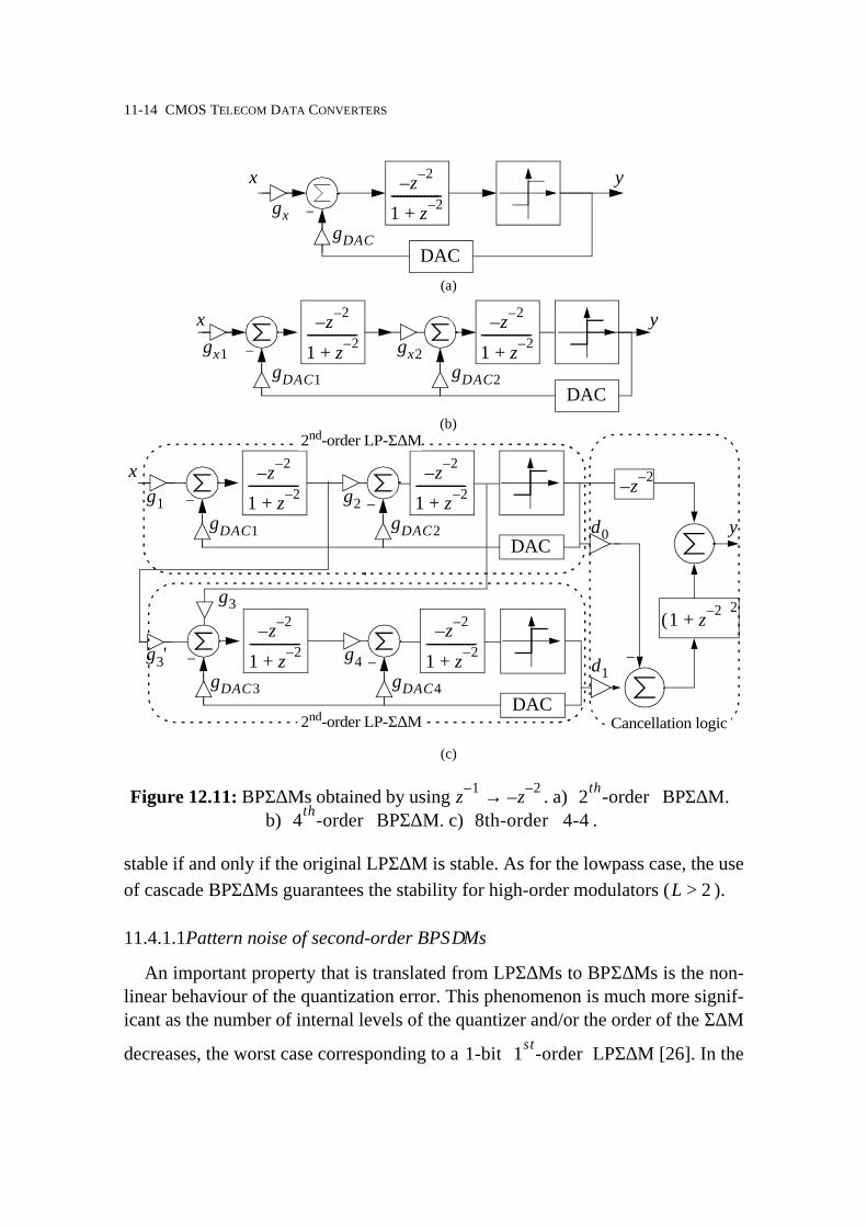
transformation in eq.(12.11) to an , LPΣ∆M. As an illustration,Fig. 12.11 shows several BPΣ∆Ms obtained by using that transformation.
Fig. 12.11(a) is a BPΣ∆M, Fig. 12.11(b) is a , and
Fig. 12.11(c) is a cascade obtained from a LPΣ∆M, a
LPΣ∆M and a cascade LPΣ∆M, respectively.The transformation in eq.(12.11) preserves all features of the original modula-
tor: , , , etc.... In addition to these characteristics, eq.(12.11) keeps the
stability properties of the original LPΣ∆Ms. In fact, the resulting BPΣ∆M will be
Z-transform
Y z( ) z 2––( )LX z( ) 1 z 2–+( )
LEq z( )+=
Figure 12.10: Zero location of for: (a) LPΣ∆M. (b) BPΣ∆M. NTF
Re(z)
Im(z)
Re(z)
Im(z)
zn 1=
zn ejπ2---=
zn ej– π2---
=
UnityCircle
UnityCircle
(a) (b)
NTF
fS 4⁄
zn j π 2⁄( )[ ]exp=
zn j π 2⁄( )[ ]exp= NR z( ) z 2––=
PQ
fn fS 4⁄=
Lth-order SNR DR
Lth-order
2Lth-order N-bit
Lth-order N-bit
2nd-order 4th-order
8th-order 4-4 1st-order
2nd-order 4th-order 2-2
PQ SNR DR
11-14 CMOS TELECOM DATA CONVERTERS
stable if and only if the original LPΣ∆M is stable. As for the lowpass case, the useof cascade BPΣ∆Ms guarantees the stability for high-order modulators ( ).
11.4.1.1Pattern noise of second-order BPΣ∆Ms
An important property that is translated from LPΣ∆Ms to BPΣ∆Ms is the non-linear behaviour of the quantization error. This phenomenon is much more signif-icant as the number of internal levels of the quantizer and/or the order of the Σ∆M
decreases, the worst case corresponding to a LPΣ∆M [26]. In the
z– 2–
1 z 2–+----------------
+
−
x y
DAC
gxgDAC
Figure 12.11: BPΣ∆Ms obtained by using . a) BPΣ∆M. b) BPΣ∆M. c) .
z 1– z 2––→ 2th-order4th-order 8th-order 4-4
(a)
(c)
z– 2–
1 z 2–+----------------
+
−
x y
DAC
gx1gDAC1
z– 2–
1 z 2–+----------------
gDAC2
gx2
(b)
z– 2–
1 z 2–+----------------
+
−
x
DAC
g1gDAC1
z– 2–
1 z 2–+----------------
gDAC2
g2
+
−
z– 2–
1 z 2–+----------------
+
−
DAC
g3'gDAC3
z– 2–
1 z 2–+----------------
gDAC4
g4
+
−
g31 z+ 2–( )
2
d1
d0
+−
z– 2–
y
+
+
2nd-order LP-Σ∆M
2nd-order LP-Σ∆M Cancellation logic
L 2>
1-bit 1st-order
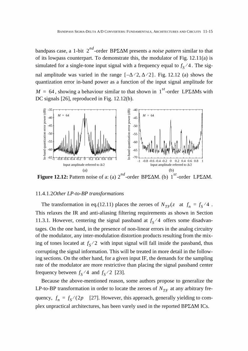
BANDPASS SIGMA-DELTA A/D CONVERTERS: FUNDAMENTALS, ARCHITECTURES AND CIRCUITS 11-15
bandpass case, a BPΣ∆M presents a noise pattern similar to thatof its lowpass counterpart. To demonstrate this, the modulator of Fig. 12.11(a) issimulated for a single-tone input signal with a frequency equal to . The sig-
nal amplitude was varied in the range . Fig. 12.12 (a) shows thequantization error in-band power as a function of the input signal amplitude for
, showing a behaviour similar to that shown in LPΣ∆Ms withDC signals [26], reproduced in Fig. 12.12(b).
11.4.1.2Other LP-to-BP transformations
The transformation in eq.(12.11) places the zeroes of at .
This relaxes the IR and anti-aliasing filtering requirements as shown in Section11.3.1. However, centering the signal passband at offers some disadvan-
tages. On the one hand, in the presence of non-linear errors in the analog circuitryof the modulator, any inter-modulation distortion products resulting from the mix-ing of tones located at with input signal will fall inside the passband, thus
corrupting the signal information. This will be treated in more detail in the follow-ing sections. On the other hand, for a given input IF, the demands for the samplingrate of the modulator are more restrictive than placing the signal passband centerfrequency between and [23].
Because the above-mentioned reason, some authors propose to generalize theLP-to-BP transformation in order to locate the zeroes of at any arbitrary fre-
quency, [27]. However, this approach, generally yielding to com-
plex unpractical architectures, has been varely used in the reported BPΣ∆M ICs.
1-bit 2nd-order
fS 4⁄
∆ 2 ∆ 2⁄,⁄–[ ]
M 64= 1st-order
Figure 12.12: Pattern noise of a: (a) BPΣ∆M. (b) LPΣ∆M. 2nd-order 1st-order
-1 -0.8 -0.6 -0.4 -0.2 0 0.2 0.4 0.6 0.8 1-65
-60
-55
-50
-45
-40
-35
In-b
and
quan
tizat
ion
erro
r pow
er (d
B)
Input amplitude referred to ∆/2
M 64=
(a) (b)
-1 -0.8 -0.6 -0.4 -0.2 0 0.2 0.4 0.6 0.8 1-70
-65
-60
-55
-50
-45
-40
In-b
and
quan
tizat
ion
erro
r pow
er (d
B)
Input amplitude referred to ∆/2
M 64=
NTF z( ) fn fS 4⁄=
fS 4⁄
fS 2⁄
fS 4⁄ fS 2⁄
NTF
fn fS 2p( )⁄=
11-16 CMOS TELECOM DATA CONVERTERS
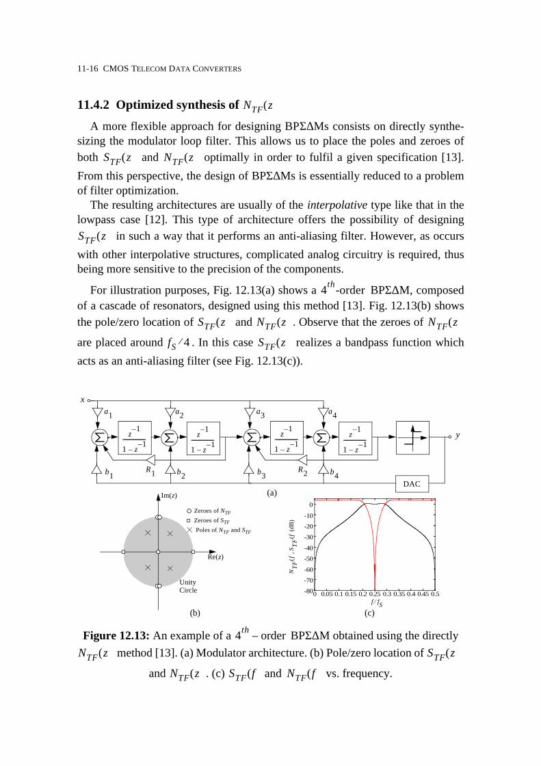
11.4.2 Optimized synthesis of
A more flexible approach for designing BPΣ∆Ms consists on directly synthe-sizing the modulator loop filter. This allows us to place the poles and zeroes ofboth and optimally in order to fulfil a given specification [13].
From this perspective, the design of BPΣ∆Ms is essentially reduced to a problemof filter optimization.
The resulting architectures are usually of the interpolative type like that in thelowpass case [12]. This type of architecture offers the possibility of designing
in such a way that it performs an anti-aliasing filter. However, as occurs
with other interpolative structures, complicated analog circuitry is required, thusbeing more sensitive to the precision of the components.
For illustration purposes, Fig. 12.13(a) shows a BPΣ∆M, composedof a cascade of resonators, designed using this method [13]. Fig. 12.13(b) showsthe pole/zero location of and . Observe that the zeroes of
are placed around . In this case realizes a bandpass function which
acts as an anti-aliasing filter (see Fig. 12.13(c)).
NTF z( )
STF z( ) NTF z( )
STF z( )
4th-order
STF z( ) NTF z( ) NTF z( )
fS 4⁄ STF z( )
Figure 12.13: An example of a BPΣ∆M obtained using the directly method [13]. (a) Modulator architecture. (b) Pole/zero location of
and . (c) and vs. frequency.
4th order–NTF z( ) STF z( )
NTF z( ) STF f( ) NTF f( )
(a)
(b) (c)
z1–
1 z1–
–----------------- z
1–
1 z1–
–-----------------
R1b1
a1 a2
b2
z1–
1 z1–
–----------------- z
1–
1 z1–
–-----------------
R2b3
a3 a4
b4DAC
Re(z)
Im(z)
UnityCircle
Zeroes of NTF
Zeroes of STF
Poles of NTF and STF
0 0.05 0.1 0.15 0.2 0.25 0.3 0.35 0.4 0.45 0.5-80
-70
-60
-50
-40
-30
-20
-10
0
NT
Ff()
S TF
f()(
dB)
,
f fS⁄
x
y

BANDPASS SIGMA-DELTA A/D CONVERTERS: FUNDAMENTALS, ARCHITECTURES AND CIRCUITS 11-17
11.4.3 Quadrature bandpass Σ∆ modulators
As stated in Section 11.2, the IR problem arising in digital superheterodynereceivers can be overcome by using quadrature mixers in both the RF and the IFsections. An obvious consequence of using quadrature mixing in the RF section isthat the IF signal is separated into two components: I and Q. Hence, two BPΣ∆Msare required as illustrated in Fig. 12.14(a), which means doubling the requiredhardware − two BPΣ∆Ms compared to only one BPΣ∆M if a simple mixer is used.This fact motivates finding new strategies that solve the problem of digitizing theI/Q components of the IF signal.
Fig. 12.14(b) shows an radio architecture that uses a complex, or quadrature,version of a BPΣ∆M, called quadrature BPΣ∆M [28]. This type of BPΣ∆Ms usesonly one ADC to perform directly the A/D conversion of both I and Q signals.
Fig. 12.15 shows a conceptual block diagram of a quadrature BPΣ∆M. Themain difference with respect to conventional BPΣ∆Ms is the complex BPFembedded in the loop. Thus, the modulator output consists of a pair of bit streams,
Figure 12.14: RF radio receivers using: (a) Conventional BPΣ∆Ms. (b) Quadra-ture BPΣ∆Ms.
(a)
(b)
RF BPFLOCommon Tuning
AntennaLNA
BPΣ∆-ADC
BPΣ∆-ADC
QuadratureMixer
DSP
I DATA
Q DATA
RF BPFLOCommon Tuning
AntennaLNA Quadrature
MixerDSP
I DATA
Q DATA
QuadratureBPΣ∆-ADC
I
Q
I
Q
Figure 12.15: Conceptual block diagram of a quadrature BPΣ∆M.
+
−
xQ
DAC
fn
Complex Filter
+
−xI
DAC
yQ
yI

11-18 CMOS TELECOM DATA CONVERTERS
one of them representing the real output and the other one the imaginary output.When combined, these two outputs form a complex digital signal which repre-sents the complex (I/Q) input signal and the shaped quantization noise.
The complex BPF in a quadrature BPΣ∆M can be realized either using DT orCT circuitry. In practice, this filter is constructed from several cross-coupled realfilters as illustrated in Fig. 12.16(a). The complex output signal is:
(12.13)
where
(12.14)
Observe that there is an analogy between complex filters and fully differentialfilters in the sense of that both architectures double the number of elementsrequired to implement a given circuit. As an illustration, Fig. 12.16(b) shows arealization of a complex 1st-order filter with a single pole at [28].
The performed by quadrature BPΣ∆Ms has complex value coefficients
and hence, it is not constrained to performing complex-conjugate zeroes or to hav-
ing a symmetric response respect to DC. This allows an BPΣ∆M toplace zeroes at without having any zero at . Therefore, the zeroes of
may be a rotated version of those of an LPΣ∆M. To illustrate this,
let us consider a complex BPΣ∆M with . This func-
tion, displayed in Fig. 12.17, presents four zeroes at .
Figure 12.16: Realization of complex filters. (a) Conceptual block diagram. (b) Complex filter with a single pole.
+
−xiRe
HRe z( )
HRe z( )
HIm z( )
HIm z( )
+−
xiIm
xoRe
xoIm
(a)
+xiRez 1–
1 z 1––---------------
+
+xiImz 1–
1 z 1––---------------
+
xoRe
xoIm
(b)bb
+
−
a 1–( )
a 1–( )
Xo z( ) H z( )Xi z( ) XoRez( ) jXoIm
+= =
XoReHRe z( )XiRe
HIm z( )XiImz( )–=
XoImHRe z( )XiIm
HIm z( )XiRez( )+=
zp a jb+=
NTF
Lth-orderL fn fn–
NTF Lth-order
4th-order NTF 1 jz 1––( )4
=
fn fS 4⁄=

BANDPASS SIGMA-DELTA A/D CONVERTERS: FUNDAMENTALS, ARCHITECTURES AND CIRCUITS 11-19
An important practical limitation of quadrature BPΣ∆Ms is due to mismatchingbetween real and imaginary channels. As a consequence, signal image compo-nents will appear in the signal band, thus corrupting the information. To reducethis effect, quadrature BPΣ∆Ms must be designed to place some of the zeroes at the image band [28]. However, this reduces the order of the quantizationnoise filtering performed by the quadrature modulator − one of its main advan-tages with respect to conventional BPΣ∆Ms.
11.4.4 N-path bandpass Σ∆ modulators
Centering the notch frequency at has multiple advantages as already
mentioned. However, in practical applications, the of BPΣ∆Ms becomesincreasingly constrained by circuit non-idealities at high sampling rates − neededto digitize signals at IF locations. To overcome this problem, some authors pro-pose the use of filters to implement the resonator transfer function [15].
Using the N-path design technique, [29], the resonator transfer function can beseparated into two high-pass filter, sampled at , such that:
(12.15)
As an illustration, Fig. 12.18 shows a 2-path BPΣ∆M [30]. The orig-inal architecture is partitioned into two interleaved paths, with the resonatorsreplaced by two high-pass filters as in eq.(12.15).
The main problem of N-path architectures is due to the gain and phase mis-matches between the different paths. This manifests itself as mirror image signals
Figure 12.17: and noise zero location for a quadrature BPΣ∆M.NTF 4th-order
-0.5 -0.4 -0.3 -0.2 -0.1 0 0.1 0.2 0.3 0.4 0.5-100
-80
-60
-40
-20
0
20
40NTF dB( )
NTF 1 jz1–
–
4=
NTF 1 z2–
+
2=
Re(z)
Im(z)
zn ejπ2---=
zn ej– π2---
=
UnityCircle
NTF 1 jz1–
–
4=
NTF 1 z2–
+
2=
Relative frequency (to fS)
NTF
fS 4⁄
DR
N-path
fS 2⁄
H z( )z 2–
1 z 2–+----------------
zp1–
1 zp1–+
----------------
zp z2
=
= =
4th-order

11-20 CMOS TELECOM DATA CONVERTERS
which appear in the signal bandwidth and corrupt the information [30].
11.4.5 Synthesis of continuous-time bandpass Σ∆ modulators
The architectures described in earlier sections assumed that the loop filter is ofthe DT type. In recent years, the increased demand for high-speed BPΣ∆Ms hasmotivated the development of BPΣ∆Ms based on CT loop filters, genericallyknown as Continuous-Time BPΣ∆Ms (CT-BPΣ∆Ms) [19][20]. This approachoffers several advantages. On the one hand, CT filters are much faster than theirDT counterparts. On the other hand, it can be shown that CT-BPΣ∆Ms provide animplicit anti-aliasing filter for out-of-band signals at no cost [22]. However, CT-BPΣ∆Ms are more sensitive to clock jitter than DT-BPΣ∆Ms. This is because theinternal clock that controls the comparison instant, also controls the rising andfalling edges of the DAC output. Hence, clock jitter errors are directly added tothe input signal [31]. Another important limitation of CT-BPΣ∆Ms is the excessloop delay contributed by each building block in the modulator loop, which canseverely degrade the quantization noise transfer function [32].†5
Fig. 12.19(a) is a conceptual block diagram of a CT-BPΣ∆M. This modulator is
5 . Section 11.5 will treat these limitations in more detail.
Figure 12.18: Conceptual diagram of a 2-path 4th-order BPΣ∆M [30].
0.4– zp1–
1 zp1–+
------------------zp
1–
1 zp1–+
------------------+
+
+
+
0.5
DAC
Φ1 Φ1
0.4– zp1–
1 zp1–+
------------------zp
1–
1 zp1–+
------------------+
+
+
+
0.5
DAC
Φ2 Φ2
X z( )Y z( )
Figure 12.19: Basic architecture of a CT-BPΣ∆M. (a) Conceptual block diagram. (b) Open loop block diagram.
+
−x yn
DAC s( )
fnH s( )
fS
x1 t( ) x1 n,(a)
DAC s( ) fnH s( )
x 0=
fS
x1 t( )E z( ) 0=
yny t( ) x1 n,
H z( )X1 z( )Y z( )-------------=
(b)

BANDPASS SIGMA-DELTA A/D CONVERTERS: FUNDAMENTALS, ARCHITECTURES AND CIRCUITS 11-21
internally a DT circuit since there is an Sampling-and-Hold (S/H) circuit insidethe loop, just at the quantizer input. This fact makes the overall loop from the out-put of the quantizer back to its input have a transfer function as illus-trated in Fig. 12.19(b). The equivalent DT loop filter transfer function is [22]:
(12.16)
where is the impulsive response of the DAC.The expression in eq.(12.16), known as pulse invariant transformation, allows
us to obtain an equivalent relation between DT- and CT-BPΣ∆Ms. Thus, the syn-thesis process of a CT-BPΣ∆M starts from a DT loop filter that satisfies therequired specifications and then it is transformed into an equivalent CT filterusing eq.(12.16). Therefore, much of the knowledge available for DT-BPΣ∆Mscan be utilized for synthesizing CT-BPΣ∆M architectures.
There are different ways of realizing the transformation ineq.(12.16) depending on the shape of , namely: NonReturn-to-Zero(NRZ), Return-to-Zero (RZ) and Half-delay Return-to-Zero (HRZ). The differ-ences among them will originate several architecture issues, specific of CT-BPΣ∆Ms. A detailed analysis of those issues − beyond the scope of this Chapter − canbe found in several works related to this subject [20][22].
11.5 BUILDING BLOCKS AND ERROR MECHANISMS IN BPΣ∆MS
The BPΣ∆M architectures described in previous sections have been consideredideal except for the quantization error. In practice, the behaviour of such architec-tures deviates from the ideal performance as a consequence of their building blockerror mechanisms. This section discusses the impact of circuit parasitics on theperformance of BPΣ∆Ms, showing their effects on the , the in-band noise
power and the harmonic distortion.The study presented here will focus on a single-loop 4th-order BPΣ∆M (4th-
BPΣ∆M) − derived from applying the transformation in eq.(12.11) to a 2nd-orderLPΣ∆M. These modulators are easy to understand and simple to design, are capa-ble of providing high resolution together with large tolerance to imperfections androbust stable operation [12]. Nevertheless, this study can be easily extended toother architectures such as multi-stage cascade architectures [33]. In these archi-tectures, the error contributions due to the first stage − usually a single-loopBPΣ∆M like that treated in this section − constitute the most significant degrading
Z-domain
H z( ) Z L 1–DAC s( )H s( )[ ]
t nTs=Z DAC τ( )h t τ–( ) τd
∞–
∞
∫t nTs=
==
DAC t( )
DT-to-CTDAC t( )
NTF
11-22 CMOS TELECOM DATA CONVERTERS
factor of the overall modulator performance.As a starting point for our study, the resonator − the main block of BPΣ∆Ms −
is analyzed. Several architectures are described as well as their circuit implemen-tation using different circuit techniques.
11.5.1 From integrators to resonators
As stated in Section 11.4.1, most of the reported BPΣ∆M architectures havebeen obtained from corresponding lowpass prototypes by applying the transfor-mation in eq.(12.11). As a consequence of this transformation, the integratorswhich form the loop filter in the original modulator become resonators with thefollowing transfer function:
(12.17)
which has their poles located at , that is, .
There are many filter structures which implement the transfer function ineq.(12.17). Fig. 12.20 shows three alternatives which has been used in BPΣ∆Ms.Fig. 12.20(a) is based on two delay elements connected in a loop, and is oftencalled Delay-loop resonator [34]. Fig. 12.20(a)-(b) are based on Lossless DirectIntegrators (LDIs) and Forward-Euler Integrators (FEIs), referred to as LDI-loopand FE-loop resonators, respectively [14]. Assuming that the scaling coefficientsare and , the three resonators in Fig. 12.20 are identical.
They have the transfer function in eq.(12.17) with for Fig. 12.20(a) and(c), and for Fig. 12.20(b).
In the presence of errors, the scaling coefficients and deviate
from their nominal values due to either capacitor ratio errors − for SC circuits [15]− or to transistor size ratio errors − in the case of SI circuits [18]. As a result ofthese errors, the poles of experience movements around their nominal
positions − different for each resonator structure as shown in Fig. 12.20.In some structures the filter poles move around the unity circle in the .
This results in the resonant frequency, , not being properly placed. This is the
case of LDI-loop resonators and FE-loop resonators under changes on .
In the Delay-loop and FE-loop structures, the effect of errors will move the reso-nator poles off the unit circle, causing instability. If the poles move inside the unitcircle, then the factor will be reduced, thus reducing the gain of at .
Although the possible instability of FE-loop resonators appears to be a draw-
Hres z( )z a–±
1 z 2–+----------------= 0 a< 2≤( )
zn 2πj±( )exp= fn fS 4⁄=
AF 1= AFB FB2, 2–=
a 2=a 1=
AF AFB FB2,
Hres z( )
Z-planefn
AFB FB2,
Q Hres fn

BANDPASS SIGMA-DELTA A/D CONVERTERS: FUNDAMENTALS, ARCHITECTURES AND CIRCUITS 11-23
back as compared to LDI-loop resonators, some authors propose to design filterswith a small instability with the objective of reducing idle tones in Σ∆Ms [35].This is still a matter of discussion. In fact, the authors in [14] reported similarexperimental results from two 2nd-order BPΣ∆Ms, one of them based on LDI-loop resonators and the other one using FE-loop resonators.
The resonator architectures shown in Fig. 12.20 can be implemented using DTcircuit techniques. As an illustration, Fig. 12.21 shows the schematics of the reso-nators in Fig. 12.20 using SC Fully Differential (FD) circuits†6 [14][34], andFig. 12.22 shows the corresponding SI (single-ended) realizations[18]. All these
6 . SC resonators can be also implemented using a two-path architecture [33][35] − notshown in this Chapter for the sake of simplicity. Their main advantage is that only oneopamp is required instead of two as in Fig. 12.21. However, a complex clock phasescheme is used, which needs to be carefully timed in order to avoid image components toappear in the signal band.
+
+
X(z) Y(z)z
1–
1 z1–
–----------------- z
1–
1 z1–
–-----------------
AF+
AFB1
AFB2(b)
Re(z)
Im(z)
Unity Circle
AFAFB1 < AFB2
AFB2 > −2
AFB2 < −2
Figure 12.20: Different filter implementations of the resonator transfer function and movement of their poles under errors in their feedback gains. a) Delay-loop.
b) LDI-loop. c) FE-loop.
+
+
X(z) Y(z)z
a–1±
z–2 a–( )–
AF
Re(z)
Im(z)
Unity Circle
AF > 1
AF < 1
AF < 1
AF > 1
(a)
+
+
X(z) Y(z)
AFB
z–1 2⁄–
1 z1–
–----------------- z–
1 2⁄–
1 z1–
–-----------------
AF
Re(z)
Im(z)
AFAFB > −2AFAFB < −2
Unity Circle
(c)

11-24 CMOS TELECOM DATA CONVERTERS
resonators have their poles placed at . This is a consequence of the
transformation. However, in some applications such as multi-standardradio receivers, it could be interesting to design the scaling coefficients to be pro-grammable. This will allow us to control without changing . This can be
done, for instance, by changing in Fig. 12.21 and the current mir-
ror output transistor size, , in Fig. 12.22(b).
In case of CT ( ) resonators like that shown in Fig. 12.23, the resonant
frequency, given by:
Figure 12.21: SC FD realizations of the resonators in Fig. 12.20. a) Delay-loop. b) LDI and FE-loop.
+
−+−
1(2)
2(1)
2(1)
1(2)
2
2
1
1
1
1
2
2+
−+−
2(1)
1(2)
1(2)
2(1)
2
1
2
1
1
2
FE-loopLDI-loop
+
−vIN
+
−vOUT
(b)
C
C
C
C
CAFB
CAFB
CAFB2
CAFB2
C
C
C
C
2
1
2
1
2
1
+
−+−
C
C
2
1
2
1
2
1
C12
1 2
C 12
1 2
C
C
2
1
2
1
2
1
+
−+−
C
C
2
1
2
1
2
1
CF12
1 2
CF12
1 21
2
C
1
2
C
+
−
vOUT
+
−
vIN
(a)
DelayElement
Integrator
Integrator
φ2(1) φ1(2)
φ1
2IBIAS AFB2IBIAS
φ1φ2(1)
AFIBIAS
ii
φ1 φ2
2IBIAS AFBIBIAS
φ1 φ1
IBIAS
io
1 1 AFB2 AF: : 1 1 AFB 1: :
Figure 12.22: SI realizations of the resonators in Fig. 12.20. a) Delay-loop and clock phase generator. b) LDI and FE-loop.
(b)
(a)φ1
φ1
φ2
φ2
φ1
φ1
φ2
φ2 φ1 φ1
IBIAS IBIAS IBIAS IBIAS AFIBIAS IBIAS
1 1 1 AF -1 1: : : : :
iIN iOUT
φ1
φ2
FE-loopLDI-loopMemory
Transistors
SamplingSwitch Scaling
Current Mirror
fn fS 4⁄=
z 1– z– 2–→
fn fS
CAFB AFB2, C⁄
AFB FB2,
gm C–
BANDPASS SIGMA-DELTA A/D CONVERTERS: FUNDAMENTALS, ARCHITECTURES AND CIRCUITS 11-25
(12.18)
can be varied by making to be programmable electronically [37].
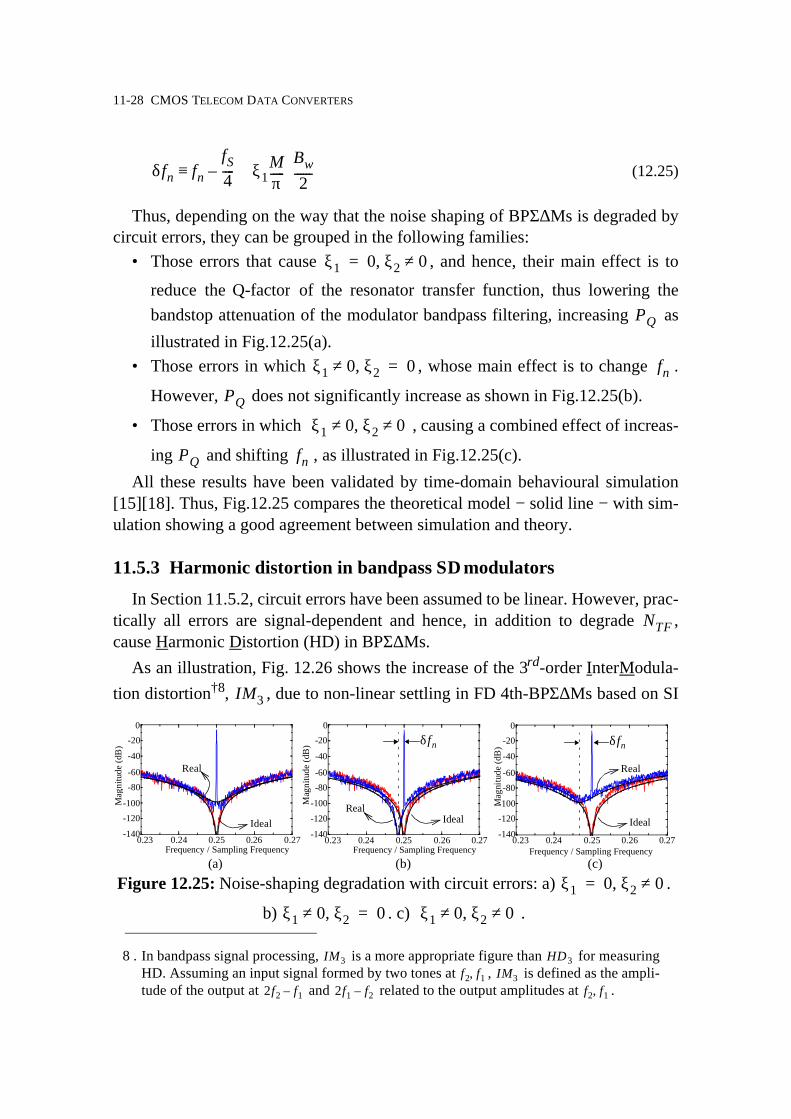
11.5.2 Quantization noise shaping degradation due to circuit errors
As discussed in previous section, LDI-loop resonators are the only ones whichremain stable under changes in their scaling coefficients. For that practical reason,this has been the resonator structure chosen for our study†7. Fig. 12.24 shows the
block diagram of a 4th-BPΣ∆M based on LDI-loop resonators.Note that the required feedback loop delay has been realized through two addi-tional delay blocks. The scaling factors can be optimized to obtain similardynamic range for both resonators. This yields to the following nominal values,
(12.19)
Ideally, the of the modulator output is given by eq.(12.2) with
(12.20)
and and are respectively given by eq.(12.8) and eq.(12.12); with
7 . A similar discussion to that presented here can be followed for the case of either FE-loopor Delay-loop based BPΣ∆Ms.
fn1
2π------gm2gmR
C1C2-------------------=
gmR
+−gm1
C1+−gm2
C2
+−
gmR
+
− +
−
vINvOUT
Figure 12.23: Conceptual schematic of a resonator.gm C–
Figure 12.24: LDI-loop based 4th-order 1-bit BPΣ∆M architecture under study.
DAC
z 1–
LDI-Loop LDI-Loop Comparator
DAC
X(z) Y(z)ARES1
ADAC1 ADAC2
Resonator1 Resonator2
z 1–
1 z 2–+------------------ z 1–
1 z 2–+------------------
z 1–
Z-domain 1-bit
ARES2 ADAC2 A– DAC1 1= = = ARES1 1 2⁄=
Z-transform
STF z 2–=
NTF 1 z 2–+( )2
=
PQ SNR

11-26 CMOS TELECOM DATA CONVERTERS
, and . However, such an ideal performance can only be
achieved provided that the resonators in Fig. 12.24 are realized without errors.In the case of SC realizations, the major sources of error that degrade the noise-
shaping of BPΣ∆Ms are [15]:• Finite operational amplifier (opamp) DC gain, represented by .
• Incomplete settling error, , caused by the limited opamp bandwidth. In a
first-order approach (single-pole), , where is the
closed-loop time constant of the SC integrator.• Mismatch capacitor ratio error, , in the scaling coefficients ( in
Fig. 12.21(b)).In the case of SI BPΣ∆Ms, the main circuit parasitics are [18]:• Finite conductance ratio error, defined as , where and
are respectively the output and input conductances of SI memory cells.• Charge injection error, , due to the charge injected, , by the sampling
switch onto the storing capacitance, , of the memory transistor (see
Fig. 12.22(b)).• Incomplete settling error, , caused by the finite bandwidth, ,
where is the transconductance of the memory cell.
• Mismatch error, , in and , of the current mirror transistors used to
implement the scaling coefficients ( in Fig. 12.22(b)).
In the presence of the above-mentioned errors, the resonator transfer function ismodified into [15][18]
(12.21)
where , and are different for each error, as Table 12.2 shows.
Replacing the transfer functions of the resonators in Fig. 12.24 with eq.(12.21),the erroneous of the 4th-BPΣ∆M is obtained, giving:
(12.22)
The zeroes of are shifted from their nominal positions at , thus
degrading the filtering performed by the resonators and making the quantization
fn fS 4⁄= N 1= L 2=
AV
εs
εs TS 2τ( )⁄–[ ]exp≡ τ
εm CAFB C⁄
εg 2 go gi⁄( )≡ go gi
εq δq
Cgs
εs gm Cgs⁄
gm
εm β VT
AFB
Hres z( ) 1 µ–( )z 1–
1 ξ1z 1– 1 ξ2–( )z 2–+ +--------------------------------------------------------≅
µ ξ1 ξ2
NTF
NTF z( ) 1 ξ1z 1– 1 ξ2–( )z 2–+ +[ ]2
≅
NTF fS 4⁄

BANDPASS SIGMA-DELTA A/D CONVERTERS: FUNDAMENTALS, ARCHITECTURES AND CIRCUITS 11-27
noise in-band power, and correspondingly, the to decrease.From eq.(12.7)-eq.(12.10) and eq.(12.22), it can be shown that the erroneous and are approximately given by [18]:
(12.23)
where
(12.24)
is the in-band quantization noise increase caused by circuit parasitics, which incombination with the expressions for given in Table 12.2, allow us to
know the maximum error permitted as a function of for a given . In addition to the loss, circuit parasitics cause a shifting of the position of
, denoted as . Solving the roots of eq.(12.22) and assuming that ,
it can be shown that:
Table 12.2: Resonator transfer function degradation with circuit errors.SC CIRCUITS
†*
* and represent the sampling and the integration capacitances, respectively.
SI CIRCUITS
µ ξ1 ξ2
AV2
AV------ 1
CS
CI------+
2–AV------ 2
CS
CI------+
2AV------
CS
CI------
Cs CI
εsTS–
2τ--------- exp≡ 2εs 4– εs 0
εm
δCAFB
CAFB----------------
δCδC-------–≡ εm εm 0
εg2go
gi-------- εq
δqCgs VGS VT–( )
Q
-----------------------------------------≡,≡ 2εg q, 0 4εg q,
εsTsgm–2Cgs
--------------- exp≡ 2εs 4– εs 4εs
εmδββ------
δVT
VGS VT–( )Q
--------------------------------–≡ εm εm 0
SNR
PQ DR
PQπ4∆2
60M5------------- P∇ Q( )= DR 15M5
2π4 P∇ Q( )-------------------------≅
PQ∇ 1 103------ 3ξ1
2 ξ22+( ) M
π----- 2
5 ξ12 ξ2
2+( )2 M
π----- 4
+ +≡
ξ1 ξ2,
M DRDR
fn δfn ξ1 ξ2 1«,
11-28 CMOS TELECOM DATA CONVERTERS
(12.25)
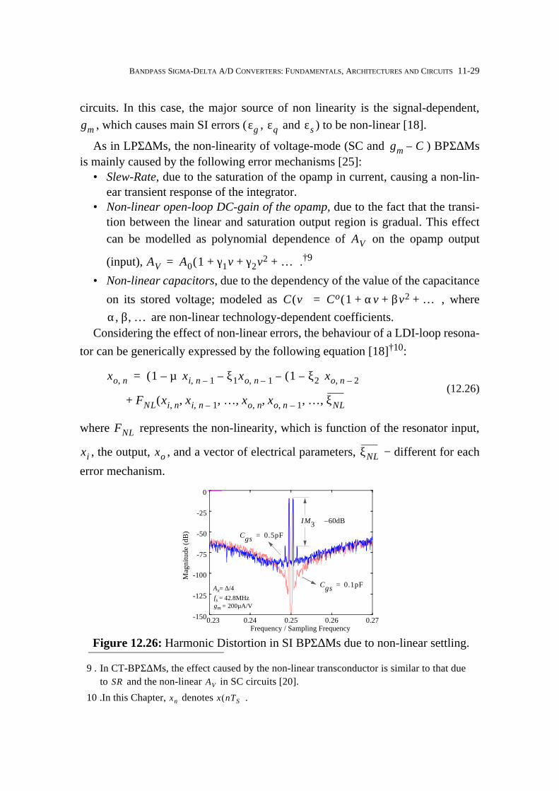
Thus, depending on the way that the noise shaping of BPΣ∆Ms is degraded bycircuit errors, they can be grouped in the following families:
• Those errors that cause , and hence, their main effect is to
reduce the of the resonator transfer function, thus lowering thebandstop attenuation of the modulator bandpass filtering, increasing as
illustrated in Fig.12.25(a).• Those errors in which , whose main effect is to change .
However, does not significantly increase as shown in Fig.12.25(b).
• Those errors in which , causing a combined effect of increas-
ing and shifting , as illustrated in Fig.12.25(c).
All these results have been validated by time-domain behavioural simulation[15][18]. Thus, Fig.12.25 compares the theoretical model − solid line − with sim-ulation showing a good agreement between simulation and theory.
11.5.3 Harmonic distortion in bandpass Σ∆ modulators
In Section 11.5.2, circuit errors have been assumed to be linear. However, prac-tically all errors are signal-dependent and hence, in addition to degrade ,cause Harmonic Distortion (HD) in BPΣ∆Ms.
As an illustration, Fig. 12.26 shows the increase of the 3rd-order InterModula-tion distortion†8, , due to non-linear settling in FD 4th-BPΣ∆Ms based on SI
8 . In bandpass signal processing, is a more appropriate figure than for measuringHD. Assuming an input signal formed by two tones at , is defined as the ampli-tude of the output at and related to the output amplitudes at .
δfn fn
fS
4----– ξ1Mπ-----
Bw
2------
≅≡
ξ1 0 ξ2 0≠,=
Q-factorPQ
Figure 12.25: Noise-shaping degradation with circuit errors: a) .
b) . c) .
ξ1 0 ξ2 0≠,=
ξ1 0 ξ2,≠ 0= ξ1 0 ξ2 0≠,≠
0.23 0.24 0.25 0.26 0.27
Mag
nitu
de (d
B)
-140
-120
-100
-80
-60
-40
-20
0
Frequency / Sampling Frequency0.23 0.24 0.25 0.26 0.27
Mag
nitu
de (d
B)
-140
-120
-100
-80
-60
-40
-20
0
Frequency / Sampling Frequency
IdealReal
δfn
Ideal
Real
Frequency / Sampling Frequency0.23 0.24 0.25 0.26 0.27
-140
-120
-100
-80
-60
-40
-20
0
Mag
nitu
de (d
B) δfn
Ideal
Real
(a) (b) (c)
ξ1 0 ξ2,≠ 0= fn
PQ
ξ1 0 ξ2 0≠,≠
PQ fn
NTF
IM3
IM3 HD3f2 f1, IM3
2f2 f1– 2f1 f2– f2 f1,
BANDPASS SIGMA-DELTA A/D CONVERTERS: FUNDAMENTALS, ARCHITECTURES AND CIRCUITS 11-29
circuits. In this case, the major source of non linearity is the signal-dependent,, which causes main SI errors ( , and ) to be non-linear [18].
As in LPΣ∆Ms, the non-linearity of voltage-mode (SC and ) BPΣ∆Msis mainly caused by the following error mechanisms [25]:
• Slew-Rate, due to the saturation of the opamp in current, causing a non-lin-ear transient response of the integrator.
• Non-linear open-loop DC-gain of the opamp, due to the fact that the transi-tion between the linear and saturation output region is gradual. This effectcan be modelled as polynomial dependence of on the opamp output
(input), .†9
• Non-linear capacitors, due to the dependency of the value of the capacitance
on its stored voltage; modeled as , where are non-linear technology-dependent coefficients.
Considering the effect of non-linear errors, the behaviour of a LDI-loop resona-tor can be generically expressed by the following equation [18]†10:
(12.26)
where represents the non-linearity, which is function of the resonator input,
, the output, , and a vector of electrical parameters, − different for each
error mechanism.
9 . In CT-BPΣ∆Ms, the effect caused by the non-linear transconductor is similar to that dueto and the non-linear in SC circuits [20].
10 .In this Chapter, denotes .
Figure 12.26: Harmonic Distortion in SI BPΣ∆Ms due to non-linear settling.
Mag
nitu
de (d
B)
Frequency / Sampling Frequency0.23 0.24 0.25 0.26 0.27-150
-125
-100
-75
-50
-25
0
Cgs 0.5pF=
Cgs 0.1pF=Ax= ∆/4fs = 42.8MHzgm = 200µA/V
IM3 60dB–≅
gm εg εq εs
gm C–
AV
AV A0 1 γ1v γ2v2 …+ + +( )=
SR AV
C v( ) Co 1 αv βv2 …+ + +( )=α β …, ,
xn x nTS( )
xo n, 1 µ–( )xi n 1–, ξ1xo n 1–,– 1 ξ2–( )xo n 2–,–=
FNL xi n, xi n 1–, … x, o n, xo n 1–, … ξNL, , , , ,( )+
FNL
xi xo ξNL

11-30 CMOS TELECOM DATA CONVERTERS
The obtainment of design equations for requires solving the time-domain
equations that govern the behaviour of BPΣ∆Ms, considering that the first resona-tor†11 behaviour is given by eq.(12.26).
Instead of deriving cumbersome expressions of for each signal-dependentparasitics − beyond the scope of this Chapter†12 −, we will center our attention ona critical effect: the non-linear sampling process. Contrary to the lowpass case,this error mechanism constitutes one of the most limiting factors in BPΣ∆Ms usedin modern telecommunication systems.
In the front-end of such systems, the input (analog) signal is changing veryquickly during the sampling phase interval. As an illustration, Fig. 12.27 showsthe transient evolution of a sinusoidal signal of amplitude and frequency
, when sampled at . In this case, corresponding to a typical input sig-
nal in BPΣ∆Ms, the signal amplitude can change up to during the sampling
phase. This change leads to a non-linear transient response of the sampling circuitwhich manifests as HD at the output of the BPΣ∆M.
For a better understanding of this phenomenon, let us consider the input stageof the SC resonators shown in Fig. 12.21(b). During the clock phase 1 (samplingphase), the input signal, , is stored in the capacitor . In practice, this circuit
is realized by using CMOS switches as shown in Fig. 12.28(a). These switches aresized such that the switch-on resistance, , verifies , thus making
the incomplete settling error negligible. This condition is not difficult to satisfy in
11 .The contribution of the second resonator to HD is attenuated by the gain of the first res-onator in the signal band. For this reason, only the first resonator contribution has to beconsidered.
12 .The interested reader is referred to [18] where a complete analysis of HD in SI BPΣ∆Msis described for each non-linear error.
IM3
IM3
Figure 12.27: Transient evolution of a input sinusoidal signal of amplitude and frequency when sampled at .
Xfi fS 4⁄≅ fS 4⁄
0 2 4 6 8-X
- X/2
0
X/2
X
Am
plitu
de
Sampling
Phase
Time (#Ts)
Xfi fS 4⁄≅ fS
X 2⁄
vIN C
Ron RonCfs 1«
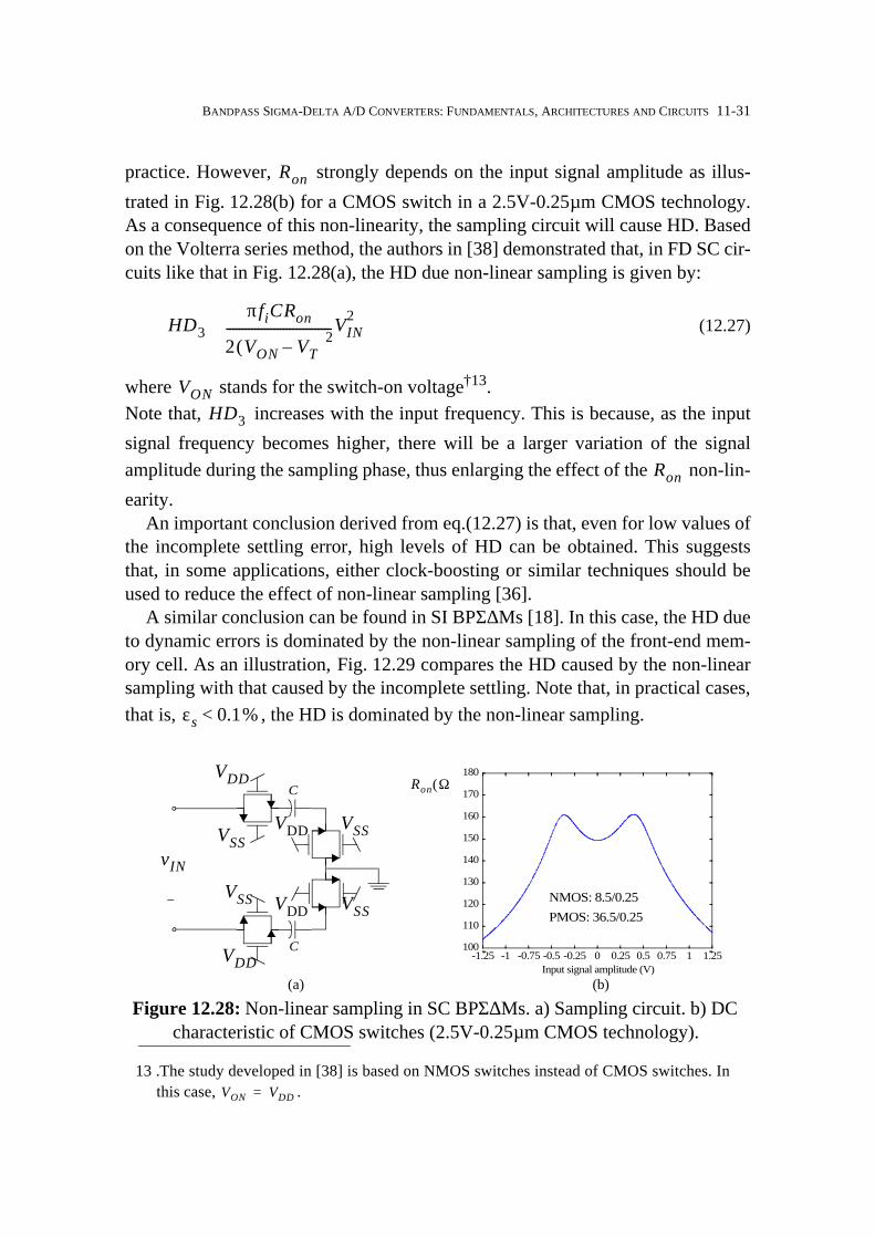
BANDPASS SIGMA-DELTA A/D CONVERTERS: FUNDAMENTALS, ARCHITECTURES AND CIRCUITS 11-31
practice. However, strongly depends on the input signal amplitude as illus-
trated in Fig. 12.28(b) for a CMOS switch in a 2.5V-0.25µm CMOS technology.As a consequence of this non-linearity, the sampling circuit will cause HD. Basedon the Volterra series method, the authors in [38] demonstrated that, in FD SC cir-cuits like that in Fig. 12.28(a), the HD due non-linear sampling is given by:
(12.27)
where stands for the switch-on voltage†13.Note that, increases with the input frequency. This is because, as the input
signal frequency becomes higher, there will be a larger variation of the signalamplitude during the sampling phase, thus enlarging the effect of the non-lin-
earity.An important conclusion derived from eq.(12.27) is that, even for low values of
the incomplete settling error, high levels of HD can be obtained. This suggeststhat, in some applications, either clock-boosting or similar techniques should beused to reduce the effect of non-linear sampling [36].
A similar conclusion can be found in SI BPΣ∆Ms [18]. In this case, the HD dueto dynamic errors is dominated by the non-linear sampling of the front-end mem-ory cell. As an illustration, Fig. 12.29 compares the HD caused by the non-linearsampling with that caused by the incomplete settling. Note that, in practical cases,that is, , the HD is dominated by the non-linear sampling.
13 .The study developed in [38] is based on NMOS switches instead of CMOS switches. Inthis case, .
VDD
VSS
C
VDD VSS
VDD
VSS VDD VSS
+
−
vIN
C-1.25 -1 -0.75 -0.5 -0.25 0 0.25 0.5 0.75 1 1.25
100
110
120
130
140
150
160
170
180
Input signal amplitude (V)
Ron Ω( )
NMOS: 8.5/0.25PMOS: 36.5/0.25
Figure 12.28: Non-linear sampling in SC BPΣ∆Ms. a) Sampling circuit. b) DC characteristic of CMOS switches (2.5V-0.25µm CMOS technology).
(a) (b)
Ron
HD3πfiCRon
2 VON VT–( )2---------------------------------VIN2≅
VON
VON VDD=
HD3
Ron
εs 0.1%<
11-32 CMOS TELECOM DATA CONVERTERS
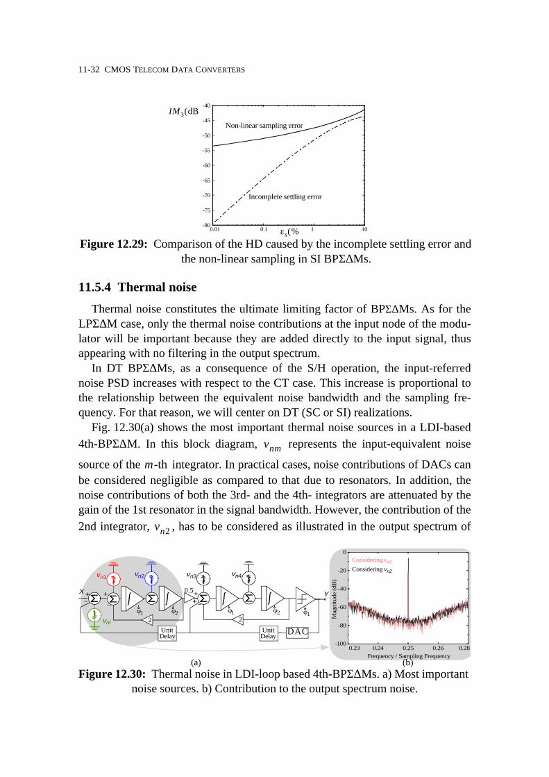
11.5.4 Thermal noise
Thermal noise constitutes the ultimate limiting factor of BPΣ∆Ms. As for theLPΣ∆M case, only the thermal noise contributions at the input node of the modu-lator will be important because they are added directly to the input signal, thusappearing with no filtering in the output spectrum.
In DT BPΣ∆Ms, as a consequence of the S/H operation, the input-referrednoise PSD increases with respect to the CT case. This increase is proportional tothe relationship between the equivalent noise bandwidth and the sampling fre-quency. For that reason, we will center on DT (SC or SI) realizations.
Fig. 12.30(a) shows the most important thermal noise sources in a LDI-based4th-BPΣ∆M. In this block diagram, represents the input-equivalent noise
source of the integrator. In practical cases, noise contributions of DACs canbe considered negligible as compared to that due to resonators. In addition, thenoise contributions of both the 3rd- and the 4th- integrators are attenuated by thegain of the 1st resonator in the signal bandwidth. However, the contribution of the2nd integrator, , has to be considered as illustrated in the output spectrum of
Figure 12.29: Comparison of the HD caused by the incomplete settling error and the non-linear sampling in SI BPΣ∆Ms.
0.01 0.1 1 10-80
-75
-70
-65
-60
-55
-50
-45
-40
εs %( )
IM3 dB( )Non-linear sampling error
Incomplete settling error
Figure 12.30: Thermal noise in LDI-loop based 4th-BPΣ∆Ms. a) Most important noise sources. b) Contribution to the output spectrum noise.
φ2
X
φ1 φ1
Y
2
+
−φ2φ1
2
+
−
0.5
+−
Unit Delay
+
DACUnit Delay
vn1 vn2 vn3 vn4
vni
(a) (b)
0.23 0.24 0.25 0.26 0.28-100
-80
-60
-40
-20
0
Mag
nitu
de (d
B)
Frequency / Sampling Frequency
Considering vn2
Considering vn1
vnm
m-th
vn2

BANDPASS SIGMA-DELTA A/D CONVERTERS: FUNDAMENTALS, ARCHITECTURES AND CIRCUITS 11-33
Fig. 12.30(b). It can be shown that the contribution of to the input-equivalent noise, ,
is twice that of that due to because in the signal band [18],
(12.28)
Therefore, the in-band power of is approximately given by:
(12.29)
where and are respectively the in-band power of and .In case that , the SNR and the DR for a sinusoidal input signal of
amplitude are respectively given by:
(12.30)
11.5.5 Jitter noise
In previous sections, ideal clock phase signals have been considered. In prac-tice, the period of the clock signal presents random variations in its nominal valueas illustrated in Fig. 12.31(a). This is due to certain intrinsic uncertainties in thetime in which clock transitions occur, known as jitter. The result is a non-uniformsampling, responsible for extra (white) noise at the output of Σ∆Ms [12].
As a consequence of jitter, it can be shown that the of DT-BPΣ∆Ms isdegraded as [31]:
(12.31)
vn2 vni
vn1
1 z 1––2
z ej2πBwTs–
=2≅
vni
Pni Pn1 2Pn2+≅
Pn1 Pn2 vn1 vn2Pni PQ>
A α∆ 2⁄=
SNRthα2∆
2
8Pni------------≅ DRth
∆2
8Pni-----------≅
δtj(a)
(b)
0.24 0.242 0.244 0.246 0.248 0.25 0.252 0.254 0.256 0.258 0.26-160
-140
-120
-100
-80
-60
-40
-20
0
∆tj 0.1ns=
fS 100MHz=
fS 10MHz=Ideal
Frequency / Sampling Frequency
Rel
ativ
e M
agni
tude
(dB
)
(c)
1 1 0 1 0
RZ
NRZ
jitter
Clock signal
Figure 12.31: Jitter noise. a) Uncertainties in the clock transitions. b) Effect on DT-BPΣ∆Ms. c) Jitter in both NRZ and RZ DAC output responses.
SNR
SNRDTj
M
4π2σj2fn
2--------------------=

11-34 CMOS TELECOM DATA CONVERTERS
where is the standard deviation of the sampling time error, †14.
Note that, as in LPΣ∆Ms, decreases with the signal frequency. How-
ever, in BPΣ∆Ms the signal frequency is a substantial fraction of , typically
, what constitutes a more limiting factor. As an illustration,
Fig. 12.31(b) shows the increase of the in-band jitter noise with in BPΣ∆Ms.
Jitter noise is specially critical in CT BPΣ∆Ms. In this type of BPΣ∆Ms, clockjitter comes from two sources†15: the S/H circuit and the DAC. The former is sub-ject to the same filtering than the quantization error, and hence, will have a smalleffect on the modulator performance. However, the DAC jitter noise is directlyadded with the input signal, thus increasing the in-band noise power. This powerincrease will depend on the impulsive response of the DAC. This is because jitteronly matters when the DAC output changes sign. Thus, as illustrated inFig. 12.31(c), for the same bit sequence, the number of DAC output rising/fallingedges per clock cycle will depend on the type of DAC response. This will mani-fest as a different degradation, given by [31]:
(12.32)
Note that, as Fig. 12.31(c) predicts, a lower degradation is achieved byusing NRZ DACs. Thus, comparing eq.(12.31) and eq.(12.32) it can be shownthat CT-BPΣ∆Ms are more sensitive to jitter than DT-BPΣ∆Ms. For instance,considering NRZ DACs in eq.(12.32) (the best case) and , the condition
(12.33)
should be satisfied to obtain the same loss in both CT- and DT-BPΣ∆Ms.
14 .The clock jitter error, represented here by parameter , behaves as a random variablewith a Gaussian distribution of standard deviation and zero mean.
15 .There is another source of jitter noise caused by comparator metastability. This non-ideal effect causes an increase of the in-band noise which can be modelled as a jitternoise as shown in [20]. This kind of jitter is often referred to as signal-dependent jitterbecause it is due to the signal-dependent comparator delay.
σj δtj
δt jσj
SNR DTj
fS
fn fS 4⁄≅
fS
SNR
SNRCTj
sinc πfnTS( )
64σj2Bw
2 M---------------------------- for NRZ DACs
sinc πfnTS( )
64TS
T0-----
2σj
2Bw2 M
--------------------------------------- for RZ DACs
≅
SNR
fn fS 4⁄≅
σj2
CTσj
2
DT
π8---
2sinc π
4--- 0.14σj
2
DT≅=
SNR

BANDPASS SIGMA-DELTA A/D CONVERTERS: FUNDAMENTALS, ARCHITECTURES AND CIRCUITS 11-35
Besides jitter, the DAC time response causes another important degradation inCT-BPΣ∆Ms which is analyzed in next section.
11.5.6 Excess loop delay in continuous-time BPΣ∆Ms
Ideally, the DAC output currents†16 should respond immediately to the quan-tizer clock edge. In practice, there exists a delay, as illustrated in the multi-feed-back CT-BPΣ∆M†17 of Fig. 12.32(a). This delay, often referred to as excess loopdelay or loop delay, is normally expressed as a fraction of the sampling period,
, where .
16 .In most of CT-BPΣ∆Ms, DACs are realized by differential pairs driven by the quantizeroutput.
17 .This architecture uses different types of DACs − each with separately feedback coeffi-cients − to obtain similar noise-shaping than that of the DT-BPΣ∆M in Fig. 12.24 [32].This strategy allows us to use resonator transfer function of the type , whichare easier to realize through circuits than the CT filters resulting from a DT-to-CTtransformation like that in eq.(12.16).
Figure 12.32: Excess loop delay. a) DAC time response in CT-BPΣ∆Ms. Effect on: b) Transient response of first resonator. c) Modulator output spectrum.
0.1 0.15 0.2 0.25 0.3 0.35 0.4-100
-50
0
0.1 0.15 0.2 0.25 0.3 0.35 0.4-100
-50
0
0.1 0.15 0.2 0.25 0.3 0.35 0.4-100
-50
0
500 550 600 650 700 750 800 850 900 950 1000-2-1012
500 550 600 650 700 750 800 850 900 950 1000-2-1012
500 550 600 650 700 750 800 850 900 950 1000-10
-5
0
5
10
1st-
Res
onat
or O
utpu
t Am
plitu
de (V
)
Time (#Ts) Frequency / Sampling Frequency
Rel
ativ
e M
agni
tude
(dB
)
(b) (c)
ρd 0.1=
ρd 0.2=
ρd 0.4=
ρd 0.1=
ρd 0.2=
ρd 0.4=
τd
outcomparator
outDAC
t
x y
g1h g2h
S/Hπ 2⁄( ) s
s2
π 2⁄( )2
+------------------------------
π 2⁄( )s
s2
π 2⁄( )2
+------------------------------
HRZ DAC
RZ DAC
g2rg4r
(a)
Resonator Resonator Comparator
s s2 ω2+( )⁄gmC
τd ρdTs= 0 ρd 1≤<
11-36 CMOS TELECOM DATA CONVERTERS
As a consequence of the poles introduced by , the noise-shaping transfer
functions, and , are modified, thus increasing the in-band noise power as
illustrated in Fig. 12.32(c). This effect becomes specially critical in telecom appli-cations, in which large values of − in the example of Fig. 12.32(b)-
(c) − may eventually make CT-BPΣ∆Ms unstable [20].Mathematically speaking, complex analyses are required to obtain the stability
condition in most common BP-CTΣ∆M architectures. Instead of that, simulation-based analyses are normally used to know the critical value of leading to insta-
bility. This simulation-based approach is used − in combination with other strate-gies such as coefficient tunning and adding extra DAC branches − to compensatefor the excess loop delay as stated in [20].
11.6 STATE-OF-THE-ART BANDPASS Σ∆ ADCS
Although the idea of translating the zeroes of from DC to any given IF
location was originally presented by Schreier and Snelgrove in 1989 [5], it wasnot until 1992 that Jantzi, Snelgrove and Ferguson published the first monolithicBPΣ∆M IC [39]. Since then, there have been a large number of ICs implementedin several technologies, with diverse circuit techniques; using different supplyvoltages.
Table 12.3 shows a summary of the CMOS BPΣ∆ ADC ICs published to thisday. For each of them, the most significant figures are shown, namely: , ,
, , , the power consumption, the characteristics of the fabrication process
and the modulator architecture. For the latter, the synthesis method employed isalso given. Note that most modulators use a single-loop architecture, obtained by
applying the transformation, which, as stated in Section 11.4.1,makes .
The BPΣ∆Ms in Table 12.3 cover multiple applications in digital wirelesscommunications, ranging from telemetering [40] to digital radio receivers [13][14][19][23][33] and modern cellular phones [22][34][41][42]. Depending on theapplication, there are different specifications for , and . Hence, it is dif-
ficult to state a measure of comparison among all reported modulators. Thus, inorder to compare different performances, the following Figure-Of-Merit ( )
will be used for BPΣ∆Ms †18:
ρd 0≠
STF NTF
ρd ρd 0.4≅
ρd
NTF
DR SNRfS fn Bw
z 1– z 2––→fn fS 4⁄=
DR Bw fn
FOM

BANDPASS SIGMA-DELTA A/D CONVERTERS: FUNDAMENTALS, ARCHITECTURES AND CIRCUITS 11-37
(12.34)
Fig. 12.33, plots vs. for the modulators in Table 12.3. Note that,
the best trade-off among power consumption, resolution and is obtained by
LP-to-BP BPΣ∆Ms, most of them using SC circuits. However, to the best of our
18 .As proposed in [25], can beused for comparative evaluation of LPΣ∆Ms. This formula, which represents the energy(expressed in picojoules) needed per conversion, is not suited to compare BPΣ∆Msbecause it does not include . However, this data constitutes one of the most importantdesign specifications.
FOM Power W( ) 1012×[ ] 2Resolution bit( ) fd Samples s⁄( )×[ ]⁄=
fn
Table 12.3: Summary of CMOS bandpass Σ∆ modulators published up to now.Author†*
* Sorted by date of publication.
DR (bit)
fS (MHz)
fn(MHz)
Bw (kHz)
Power(mW)
Technology Architecture
Jantzi’93 [13] 10.2 1.825 0.455 8 210 3µm DP / 5V 4th, Optim.
Longo’93 [34] 15 7.2 1.8 30 -- 1µm DP / 5V 4th,
Song’95 [41] 9 8 2 30 0.8 2µm DP / 3.3V 4th,
Hairapetian’96 [33] 11.7 13 3.25 200 14.4 0.8µm DP / 3V 4-2,
André’96 [43] 8 8 2 64 8 0.5µm DP / 3.3V 6th,
Liu’97 [44] 11.8 0.827 0.413 2 -- 2µm DP / 5V 4th, Optim.
Cormier’97 [21] 9.5 1.250.25-.375 6.25 -- 2µm DP / 5V 4th,
Ong’97 [30] 12.2 80 20 200 72 0.6µm SP 3.3V 4th, Jantzi’97 [28] 10.8 10 3.75 200 130 0.8µm SP / 5V 4th, Quadrature
André’98 [45] 9.2 4 1 200 19 0.5µm DP / 3V 3th-3bit, Optim.
Bazarjani’98 [46] 6.7 40 20 1250 65 0.5µm DP / 5V 2nd,
Chuang’98 [47] 13 0.5 0.125 0.5 -- 2µm DP / 5V 6th, Optim.
Van Engelen’99 [19]11.7 40 9.15 200
60 0.5µm DP / 5V 6th, CT10.8 80 10.7 200
Park’99 [48] 12.2 20 5 200 180 0.65µm SP / 4V 4th,
Tabatabaei’99 [42] 13 80 20 1250 90 0.25µm DP/ 2.5V 6th,
Tonietto’99 [49] 12.7 42.8 10.7 200 80 0.35µm SP / 3.3V 6th, Optim.
Bazarjani’99 [50] 9.4 68 17 1250 48 0.6µm DP / 3V 4-4, Tao’99 [51] 8 400 100 200 330 0.35µm SP/ 3.3V 2nd, CTTabatabaei’00 [52] 12 64 16 2000 110 0.25µm SP/ 2.5V 6th, 2-path
Cusitano’00 [53] 12 37.05 10.7 200 116 0.35µm SP/ 3.3V 6th, Optim.
Cheung’01[54] 6.7 42.8 10.7 200 12 0.35µm SP/ 1V 2nd,
Salo’02 [36] 11.7 80 20 270 56 0.35µm?P/ 3V 4th, 6.7 3840Ueno’02 [55] 12.6 10 0.566 250 77 0.25µm DP/ 2.5V 2-2, 3bit
NTF
z1–
z2–
–→
z1–
z2–
–→
z1–
z2–
–→
z1–
z2–
–→
NTF
z1–
z2–
–→
z1–
z2–
–→
NTF
z1–
z2–
–→
NTF
z1–
z2–
–→
z1–
z2–
–→
NTF
z1–
z2–
–→
NTF
z1–
z2–
–→
z1–
z2–
–→
FOMBPPower (mW)
2DR bits( ) fn MHz( )×-------------------------------------------------=
FOMBP Bw
fn

11-38 CMOS TELECOM DATA CONVERTERS
knowledge, only a few of them were integrated in a standard CMOS process[30][48][54]. This is due to the fact that SC circuits are very sensitive to capacitorlinearity and most linear capacitor structures are formed by two poly layers − notavailable in standard processes.
This fact has motivated the exploration of other analog techniques compatiblewith standard, digital VLSI technologies. This is the case of SI circuits, whichduring the last few years have been used for different analog functions, includingfiltering and A/D conversion [18][56][57].
In the case of LPΣ∆Ms, the potential advantages of SI circuits have not beendemonstrated in practice. To illustrate this, Fig. 12.34 compares the of both
1,E-04
1,E-03
1,E-02
1,E-01
1,E+00
1 10 100 1000 10000
B w (kHz)
FO
MB
P (
pJ)
SC Optim. NTF
CT Optim. NTF
CT Single-loop
SC LP-to-BP
SC Quadrature
SI LP-to-BP
Figure 12.33: vs. for the modulators in Table 12.3.FOMBP Bw
AM, IS-54 FM, GSM, PCS
UMTS, DECTIS-95BLUETOOTH
Figure 12.34: vs. (DOR) for both SI and SC LPΣ∆Ms.FOM fd
1,0E+00
1,0E+01
1,0E+02
1,0E+03
1,0E+04
0,0001 0,01 1 100
DOR (MS/s)
FOM
1(pJ
) SCSI
FO
M (
pJ)
DOR (MS/s)
FOM

BANDPASS SIGMA-DELTA A/D CONVERTERS: FUNDAMENTALS, ARCHITECTURES AND CIRCUITS 11-39
SI and SC LPΣ∆Ms reported in literature. Note that the performance obtained bySI circuits is worse than that obtained by SC circuits. Observe that, while most SCmodulators feature an below about , practically all SI modulatorsobtain an above .
However, as demonstrated in [18], the performance of SI Σ∆Ms can beenhanced by means of a design methodology supported by a systematic analysisand modeling of error mechanisms. This is illustrated in Fig. 12.33, where the per-formance of the SI BPΣ∆Ms reported in [18] − intended for digital radio receivers− is compared to that of the BPΣ∆Ms in Table 12.3. It can be seen that Fig. 12.33shows a better performance comparison between SI and SC than in LPΣ∆Ms(Fig. 12.34), thus demonstrating that the SI technique is a viable alternative to thetraditional SC technique for implementing BPΣ∆Ms in deep submicron CMOStechnologies.
REFERENCES
[1] A.A. Abidi: “Low-Power Radio-Frequency ICs for Portable Communica-tions”, Proc. of the IEEE, Vol.83, pp. 544-569, April 1995.
[2] J. Mitola: “Technical Challenges in the Globalization of Software Radio”,IEEE Comm. Mag., pp. 84-89, February 1999.
[3] B. Bing and N. Jayant: “A Cellphone for all Standards”, IEEE Spectrum, pp.34-39, May 2002.
[4] H. Inose, Y. Yasuda and J. Murakami: “A Telemetering System by Code Mod-ulation − ∆-Σ Modulation”, IRE Transactions on Space Electronics and Telem-etry, Vol. 8, pp. 204-209, September 1962.
[5] R. Schreier and M. Snelgrove: “Bandpass Sigma-Delta Modulation”, Electron-ics Letters, Vol. 25, pp. 1560-1561, November 1989.
[6] M. Ismail: “Introduction to RF CMOS IC Design for Wireless Applications”,Tutorial 2 in the 2001 Conference on Design of Circuits and Integrated Sys-tems, November 2001.
[7] A. R. Feldman: “High-Speed, Low-Power Sigma-Delta Modulators for RFBaseband Channel Applications”, Ph. D. Dissertation, University of Califor-nia, Berkeley, 1998.
[8] B. Razavi: “RF Microelectronics”. Prentice-Hall, 1998.[9] T.H. Lee: “The Design of CMOS Radio-Frequency Integrated Circuits”, Cam-
bridge University Press, 1998.[10] L. Breems and J.H. Huijsing: “Continuous-Time Sigma-Delta Modulation for
A/D Conversion in Radio Receivers”. Kluwer Academic Publishers, 2001.[11] T. Burger and Q. Huang: “A 13.5-mW 185-Msample/s ∆Σ Modulator for
UMTS/GSM Dual-Standard IF Reception”, IEEE Journal of Solid-State Cir-cuits, Vol. 36, pp. 1868-1878, December 2001.
FOM 10pJFOM 100pJ

11-40 CMOS TELECOM DATA CONVERTERS
[12] S.R. Norsworthy, R. Schreier, G.C. Temes: “Delta-Sigma Converters. Theory,Design and Simulation”. IEEE Press, 1997.
[13] S.A. Jantzi, M. Snelgrove and P.F. Ferguson: “A fourth-order Bandpass sigma-delta Modulator”, IEEE J. Solid-State Circuits, Vol. 28, pp. 282-291, March1993.
[14] F.W. Singor and W. M. Snelgrove: “Switched-Capacitor Bandpass Delta-Sigma A/D Modulation at 10.7 MHz”, IEEE J. Solid-State Circuits, pp. 184-192, March 1995.
[15] A.K. Ong: “Bandpass Analog-to-Digital Conversion For Wireless Applica-tions”, Ph. D. Dissertation, Stanford University, 1998.
[16] R.G. Vaughan, N.L. Scott and D. Rod White: “The Theory of Bandpass Sam-pling”, IEEE Trans. on Signal Processing, Vol. 39, pp 1973-1984, September1991.
[17] P.H. Gailus, W. J. Turney, and F. R. Yester: “Method and Arrangement for aSigma Delta Converter for Bandpass Signals”, U.S. Patent 4,857,828, filedJan. 28 1988, issued Aug. 15 1989.
[18] J.M. de la Rosa, B. Pérez-Verdú and A. Rodríguez-Vázquez: “SystematicDesign of CMOS Switched-Current Bandpass Sigma-Delta Modulators forDigital Communication Chips”. Kluwer Academic Publishers, 2002.
[19] J. Van Engelen and R. Van de Plassche: “Bandpass Sigma Delta Modulators”.Kluwer Academic Publishers, 1999.
[20] J. A. Cherry and W. M. Snelgrove: “Continuous-Time Delta-Sigma Modula-tors for High-Speed A/D Conversion: Theory, Practice and Fundamental Per-formance Limits”. Kluwer Academic Publishers, 2000.
[21] R. F. Cormier, T. L. Sculley, and R. H. Bamberger: “A Fourth Order BandpassDelta-Sigma Modulator with Digitally Programmable Passband Frequency”,Int. Journal of Analog Integrated Circuits and Signal Processing, pp. 217-229,1997.
[22] O. Shoaei and W. M. Snelgrove: “Design and Implementation of a Tunable40MHz-70MHz Gm-C Bandpass ∆Σ Modulator”, IEEE Trans. on Circuits andSystems-II, Vol. 44, pp. 521-530, July 1997.
[23] L. Louis, J. Abcarius, and G. W. Roberts: “An Eighth-Order Bandpass ∆ΣModulator for A/D Conversion in Digital Radio”, IEEE Journal of Solid-StateCircuits, pp. 423-431, April 1999.
[24] R. Schreier and M. Snelgrove: “Decimation for Bandpass Sigma-Delta Ana-log-To-Digital Conversion”, Proc. 1990 IEEE Int. Symp. Circuits and Systems,pp. 1801-1804, May 1990.
[25] F. Medeiro, B. Pérez-Verdú and A. Rodríguez-Vázquez: “Top-down Design ofHigh-Performance Sigma-Delta Modulators”, Kluwer Academic Publishers,1999.
[26] J.C. Candy and O.J. Benjamin: “The Structure of Quantization Noise from

BANDPASS SIGMA-DELTA A/D CONVERTERS: FUNDAMENTALS, ARCHITECTURES AND CIRCUITS 11-41
Sigma-Delta Modulation”, IEEE Trans. on Circuits and Systems - I, pp. 1316-1323, September 1981.
[27] Z.X. Zhang, G.C. Temes and Z. Czamul: “Bandpass Sigma-Delta convertorusing two-path multibit structure”, Electronics Letters, Vol.27, pp. 2008-2009,October 1991.
[28] S.A. Jantzi, K. W. Martin, and A. S. Sedra: “Quadrature Bandpass ∆Σ Modula-tion for Digital Radio”, IEEE J. Solid-State Circuits, Vol. 32, pp. 1935-1949,December 1997.
[29] R. Gregorian, G. C. Temes: “Analog MOS Integrated Circuits For SignalProcessing”. John Wiley&Sons, 1986.
[30] A.K. Ong and B.A. Wooley: “A Two-Path Bandpass Σ∆ Modulator for DigitalIF Extraction at 20MHz”, IEEE Journal of Solid-State Circuit, Vol. 32, pp.1920-1933, December 1997.
[31] H. Tao, J.M. Khoury: “Analysis of Timing Jitter in Bandpass Sigma-DeltaModulators”, IEEE Trans. on Circuits and Systems-II, pp. 991-1001, August1999.
[32] O. Shoaei and W. M. Snelgrove: “A multi-feedback design for LC bandpassDelta-Sigma Modulators”, Proc. 1995 IEEE Int. Symp. Circuits and Systems,pp. 171-173, May 1995.
[33] A. Hairapetian: “An 81-MHz IF Receiver in CMOS”, IEEE Journal of Solid-State Circuits, pp. 1981-1986, December 1996.
[34] L. Longo and H. Bor-Rong: “A 15b 30kHz Bandpass Sigma-Delta Modula-tor”, Proceeding 1993 IEEE Int. Solid-State Circuit Conference, pp. 226-227,March 1993.
[35] R. Schreier: “On the use of chaos to reduce idle-channel tones in delta-sigmamodulators”, IEEE Trans. on Circuits and Systems - Part I, pp. 539-547,August 1994.
[36] T. Salo, S. Lindfors and K. Halonen: “A 80-MHz Bandpass Σ∆ Modulator fora 100-MHz IF Receiver”, IEEE J. Solid State Circuits, Vol. 37, pp. 798-808,July 2002.
[37] G. Raghavan, J.F. Jensen, J. Laskowski, M. Kardos, M. G. Case, M. Sokolichand S. Thomas: “Architecture, Design, and Test of Continuous-Time TunableIntermediate-Frequency Bandpass Delta-Sigma Modulators”, IEEE J. Solid-State Circuits, pp. 5-13, January 2001.
[38] W. Yu, S. Sen and B. H. Leung: “Distortion Analysis of MOS Track-and-HoldSampling Mixers Using Time-Varying Volterra Series”, IEEE Trans. Circuitsand Systems - II, Vol. 46, pp. 101-113, February 1999.
[39] S.A. Jantzi, W.Martin Snelgrove, and P. F. Ferguson: “A 4th-Order BandPassSigma-Delta Modulator”, Proc. of 1992 IEEE Custom Integrated Circuit Con-ference, pp. 16.5.1-4, May 1992.
[40] O.Norman: “A BandPass Delta-Sigma Modulator For Ultrasound Imaging at

11-42 CMOS TELECOM DATA CONVERTERS
160MHz Clock Rate”, IEEE Journal of Solid-State Circuits, pp. 2036-2041,December 1996.
[41] B.S. Song: “A Fourth-Order Bandpass Delta-Sigma Modulator with ReducedNumber of Op Amps”, IEEE Journal of Solid-Stated Circuits, Vol. 25, pp.1309-1315, December 1995.
[42] A. Tabatabaei, B. Wooley: “A Wideband Bandpass Sigma-Delta Modulatorfor Wireless Applications”, IEEE Int. Symp. on VLSI Circuits, pp. 91-92, 1999.
[43] E. André, D. Morche, F. Balestro and P. Senn: “A 2-path Σ∆ Modulator forBandpass Application”, Proc. of IEEE-CAS Workshop on Analog and MixedIC Design, pp. 87-91, September 1996.
[44] H. Liu, X. Yu, T. Sculley and R. H. Bamberger: “A Fourth Order BandpassDelta-Sigma A/D Converter with Input Modulation Network and DigitallyProgrammable Passband”, Proc. 1997 IEEE Int. Symp. Circuits and System,pp. 385-388, May 1997.
[45] E. André, G. Martel, D. Morche, and P. Senn, “A Bandpass A/D Converter andits I/Q Demodulator for Integrated Receivers”, Proceedings of the 24th Euro-pean Solid-Stated Circuits Conference, ESSCIRC’98, pp. 416-419, September1998.
[46] S. Bazarjani, W.M. Snelgrove: “A 160MHz Fourth-Order Double-Sampled SCBandpass Sigma-Delta Modulator”, IEEE Trans. Circuits and Systems-II, Vol.45, pp. 547-555, May 1998.
[47] S. Chuang, H. Liu, X. Yu, T.L. Sculley, R. H. Bamberger: “Design and Imple-mentation of Bandpass Delta-Sigma Modulators Using Half-Delay Integra-tors”, IEEE Trans. Circuits and Systems-II, Vol. 45, pp. 535-546, May 1998.
[48] J. Park, E. Joe, M. Choe, B. Song: “A 5-MHz IF Digital FM Demodulator”,IEEE Journal of Solid-State Circuit, Vol. 34, pp. 3-11, January 1999.
[49] D. Tonietto, P. Cusinato, F. Stefani, A. Baschirotto: “A 3.3V CMOS 10.7MHz6th-order bandpass Σ∆ Modulator with 78dB Dynamic Range”, Proceedings ofthe 25th European Solid-Stated Circuits Conference, ESSCIRC’99, pp. 78-81,September 1999.
[50] S. Bazarjani, S. Younis, J. Goldblatt, D. Butterfield, G. McAllister, S. Cicca-relli: “An 85MHz IF Bandpass Sigma-Delta Modulator for CDMA Receivers”,Proceedings of the 25th European Solid-Stated Circuits Conference, ESS-CIRC’99, pp. 266-269, September 1999.
[51] H. Tao, J.M. Khoury: “A 400-MS/s Frequency Translating Bandpass Sigma-Delta Modulator”, IEEE J. Solid State Circuits, Vol. 34, pp. 1741-1752,December 1999.
[52] A. Tabatabaei and B. Wooley: “A Two-path Bandpass Sigma-Delta Modulatorwith Extended Noise Shaping”, IEEE J. Solid State Circuits, Vol. 35, pp.1799-1809, December 2000.
[53] P. Cusitano, F. Stefani and A. Baschirotto, “A 73dB SFDR 10.7MHz 3.3V

BANDPASS SIGMA-DELTA A/D CONVERTERS: FUNDAMENTALS, ARCHITECTURES AND CIRCUITS 11-43
CMOS Bandpass Σ∆ Modulator sampled at 37.05MHz”, Proc. of the 26thEuropean Solid-State Cicuits Conference, pp. 80-83, September 2000.
[54] V. S. L. Cheung, H.C. Luong and W.H. Ki, “A 1V 10.7MHz Switched-OpampBandpass Σ∆ Modulator using Double-Sampling Finite-Gain CompensationTechnique”, 2001 IEEE Int. Solid-State Circuit Conference, pp. 52-53, Febru-ary 2001.
[55] T. Ueno, A. Yasuda, T. Yamaji and T. Itakura, “A Fourth-Order Bandpass ∆−ΣModulator Using Second-Order Bandpass Noise-Shaping Dynamic ElementMatching”, IEEE J. Solid State Circuits, Vol. 37, pp. 809-816, July 2002.
[56] N.Tan, Switched-Current Design and Implementation of Oversampling A/DConverters. Kluwer Academic Publishers 1997.
[57] B.E. Jonsson: Switched-Current Signal Processing and A/D Conversion Cir-cuits - Design and Implementation. Kluwer Academic Publishers 2000.

11-44 CMOS TELECOM DATA CONVERTERS