Embed Size (px)
Citation preview

Electrical and Computer Engineering Faculty Publications Electrical & Computer Engineering
11-2004
A 2 GHz Bandpass Analog to Digital Delta-sigma Modulator for A 2 GHz Bandpass Analog to Digital Delta-sigma Modulator for
CDMA Receivers with 79 DB Dynamic Range in 1.23 MHz CDMA Receivers with 79 DB Dynamic Range in 1.23 MHz
Bandwidth Bandwidth
Elias H. Dagher Skyworks Solutions, Inc
Peter Stubberud University of Nevada, Las Vegas, [email protected]
Wesley K. Masenten Masenten and Associates
Matteo Conta RFDomus
Thang Victor Dinh Unav Microelectronics Follow this and additional works at: https://digitalscholarship.unlv.edu/ece_fac_articles
Repository Citation Repository Citation Dagher, E. H., Stubberud, P., Masenten, W. K., Conta, M., Dinh, T. V. (2004). A 2 GHz Bandpass Analog to Digital Delta-sigma Modulator for CDMA Receivers with 79 DB Dynamic Range in 1.23 MHz Bandwidth. IEEE Journal on Solid State Circuits, 39(11), 1819-1828. IEEE. https://digitalscholarship.unlv.edu/ece_fac_articles/143
This Postprint is protected by copyright and/or related rights. It has been brought to you by Digital Scholarship@UNLV with permission from the rights-holder(s). You are free to use this Postprint in any way that is permitted by the copyright and related rights legislation that applies to your use. For other uses you need to obtain permission from the rights-holder(s) directly, unless additional rights are indicated by a Creative Commons license in the record and/or on the work itself. This Postprint has been accepted for inclusion in Electrical and Computer Engineering Faculty Publications by an authorized administrator of Digital Scholarship@UNLV. For more information, please contact [email protected].

Reference Number: M7541 (Regular Paper) 1
Abstract—This paper presents the design of a second order,
single-bit, analog-to-digital, continuous-time Delta-Sigma
Modulator (CT-M) that can be used in wireless CDMA
receivers. The CT-M samples at 2 GHz, consumes 18 mW at
1.8 V and has a 79 dB signal-to-noise ratio (SNR) over a 1.23
MHz bandwidth. The CT-M was fabricated in a 0.18 m, 1-
poly, 6-metal, CMOS technology and has an active area of
approximately 0.892 mm2. The M’s critical performance
specifications are derived from the CDMA receiver
specifications.
Index Terms—Analog-digital conversion, Code division
multiple access, Continuous time delta-sigma modulation,
CMOS, High-speed integrated circuit
I. INTRODUCTION
Recently, a family of receiver architectures, often called
digital radio receivers, has gained interest in the wireless
communications industry. Such architectures include the zero
intermediate frequency (IF) (ZIF) receiver and the complex
low IF (CLIF) or Weaver architecture receiver [1]. Unlike
superheterodyne architectures that perform channel filtering
and automatic gain control (AGC) after the first down
conversion and digitize the received signal after a second
down conversion, digital radio architectures digitize the
received signal after a single down conversion and perform
AGC and channel filtering digitally. As a result, digital radio
receivers rely mainly on digital circuitry, and can therefore be
programmed to operate as multimode receivers. Also, because
the density of digital circuitry is far greater than that of RF
circuitry, digital radio receivers can be fabricated on a single
Manuscript received January 14, 2004; revised May 30, 2004. The authors were with Ditrans Corporation, Irvine, CA during this work.
E. H. Dagher is with Skyworks Solutions, Inc., Irvine, CA 92612 USA (e-
mail: [email protected]). P. A. Stubberud is with the University of Nevada, Las Vegas, NV 89154
USA (e-mail: [email protected]).
W. K. Masenten is with Masenten and Associates, Irvine, CA 92612 USA (e-mail: [email protected]).
M. Conta is with RFDomus, Irvine, CA 92613 USA (e-mail:
[email protected] ). T. V. Dinh is with Unav Microelectronics, Irvine, CA 92618 USA (e-mail:
integrated circuit (IC).
Because digital radio receivers do not perform analog
channel filtering before digitizing the received signal, the
analog-to-digital converters (ADCs) in digital radio receivers
must have a larger dynamic range and better linearity than
ADCs in superheterodyne receivers. Additionally, unlike
superheterodyne receivers which use the receiver’s analog
channel select filters as the ADCs’ anti-aliasing filter, digital
radios typically provide little or no channel filtering in front of
the receiver’s ADCs. As a result, the ADCs in digital radio
receivers need to provide both their own anti-aliasing filters
and sample at higher rates than ADCs in superheterodyne
receivers. Because continuous time delta-sigma modulators
(CT-) can be designed to have large dynamic ranges,
sample at very high rates, provide inherent anti-aliasing
filtering, and are smaller and consume less power than many
other ADC architectures with similar specifications, CT-s
are a natural choice for a digital radio receiver’s ADCs.
Several high-speed CT-Ms that can meet many digital
radio specifications have been reported in literature. For
example, [2], [3], and [4] report on several CT-Ms that
have large dynamic ranges and can sample at rates from 4
GHz to 18 GHz; however, because these modulators were
fabricated using heterojunction bipolar transistors (HBTs) on
an InP substrate and because these modulators consume 1.5 W
to 3.2 W of power, they are not amenable to low power single
chip digital radio designs. [5] and [6] report on SiGe CT-
Ms that have large dynamic ranges and can sample at rates
up to 4 GHz; however, each of these modulators consumes
hundreds of mWs of power, and as a result are not amenable
to providing low power, single chip implementations of digital
radio receivers.
Several CMOS CT-Ms that can meet many digital radio
specifications have also been reported in literature. For
example, [7] reports on a 48 MHz second order multi-bit CT-
M that consumes 2.2 mW; however it only achieves 68
dB/1 MHz DR. [8] reports on a fifth order feed-forward CT-
M that consumes 4.1 mW and achieves a DR of 83
dB/1.228 MHz. However, the feed-forward architecture of [8]
requires an anti-aliasing filter in front to supplement its slow
signal transfer function roll-off. Both of these CMOS designs
add complexity to the M by using higher orders, multi-bit
feedback, or anti-aliasing filters.
Elias H. Dagher, Peter A. Stubberud, Senior Member, IEEE, Wesley K. Masenten, Life Member,
IEEE, Matteo Conta, and Thang Victor Dinh
A 2 GHz Analog-to-Digital Delta-Sigma
Modulator for CDMA Receivers with 79 dB
Signal-to-Noise Ratio in 1.23 MHz Bandwidth

Reference Number: M7541 (Regular Paper) 2
This paper describes a 2 GHz, CMOS, continuous-time,
single-bit, delta-sigma modulator that uses a simple robust
second order implementation and consumes 18 mW. Because
of the M’s architecture and high sampling rate, this M
has a large dynamic range and can provide inherent anti-
aliasing filtering over a large bandwidth of frequencies. As a
result, it can be used in low cost, single chip, CMOS
implementations of both ZIF and CLIF receiver architectures
for CDMA, GSM, and AMPS cellular standards.
Although this M can be used for CDMA, GSM, and
AMPS standards, Section II of this paper only derives the
M’s performance requirements from the CDMA2000
specifications [9]. Section III describes the delta-sigma
modulator (M) architecture. Section IV describes the
M’s circuit design and Section V reports on test results.
II. DELTA-SIGMA PERFORMANCE REQUIREMENTS
Fig. 1 shows the basic architecture of a CLIF and ZIF
digital radio receiver. Similar to a superheterodyne receiver,
the radio frequency (RF) signal that is received from the
antenna is amplified by a low noise amplifier (LNA) via a
duplexer. Because CDMA carrier signals range from 1930
MHz to 1990 MHz, LNAs for CDMA receivers are typically
tuned to those frequencies and provide some small amount of
RF filtering about those frequencies. In a ZIF architecture, the
two parallel mixers directly convert the amplified RF signal to
a complex base-band or complex ZIF signal. In a CLIF
architecture, the two parallel mixers convert the amplified RF
signal to a CLIF signal. The low IF is selected at a frequency
such that DC offsets and flicker noise do not affect the
receiver’s performance. This paper’s CLIF is 2.5 MHz. In
both the ZIF and CLIF architectures, the outputs of the mixers
are digitized using two parallel ADCs, which are assumed to
be CT-Ms in this paper. In both ZIF and CLIF
architectures, channel selection and demodulation are then
performed digitally. Because the ZIF and CLIF architectures
do not perform analog AGC or analog channel filtering before
digitizing the received signal, the performance requirements of
the Ms closely reflect the RF front-end receiver’s
performance requirements which include dynamic range,
signal-to-noise ratio (SNR), and linearity which is typically
specified as spurious free dynamic range (SFDR).
A. Sensitivity (Dynamic Range and SNR)
The dynamic range of a system is defined as the ratio of the
system’s maximum input signal power to the system’s
minimum detectable input signal power or receiver sensitivity
over a specified bandwidth [9]. The required dynamic range
for a receiver can then be specified as the ratio of the largest
in-band or out-of-band signal power to the minimum receiver
sensitivity. A CDMA receiver’s sensitivity requirement is set
by the single tone desensitization test in [9]. In this test, the
maximum input signal power at the antenna is -30 dBm over a
bandwidth of 1.23 MHz. The duplexer can have 3 to 5 dB of
loss. Assuming a 3 dB power loss through the duplexer, the
LNA’s maximum input signal power, PLNA_in, is -33 dBm over
1.23 MHz. For the purposes of this paper, the receiver’s
minimum sensitivity is determined as the receiver’s minimum
input signal noise power, which is the thermal noise power,
PThermal, over a 1.23 MHz bandwidth, at -113.1 dBm times the
receiver’s noise figure (NF). Assuming a NF of 5 dB, the
receiver’s dynamic range specification, DRRx, over 1.23 MHz
can be calculated as
.1.75
5)1.113(33
)()()(_
_
dB
dBdBmdBm
dBNFdBmPdBmP
NFP
PDR
ThermalinLNA
Thermal
inLNARx
(1)
Because no filtering or gain control exists between the
output of the LNA/mixer chain and the Ms, each M’s
minimum sensitivity can be determined by allocating a NF,
NF, to each M and then calculating the resulting required
maximum noise floor level. To determine a NF for each M,
assume that the LNA/mixer chain is budgeted 4 dB (2.5) of
the 5 dB (3.16) noise figure. The receiver’s NF is the sum of
the LNA/mixer chain’s NF and the M’s NF. Thus, the
Ms can contribute only -1.8 dB (0.66) of noise figure to the
receiver. This noise figure for the Ms must also include any
in channel spurious elements introduced by the M. Because
the in-phase (I) and quadrature (Q) information signals
combine coherently and the I and Q noise signals combine as
the sum of the squares, the combined I and Q channels
inherently provide a 3 dB SNR gain, denoted as ACC. Thus,
each M’s dynamic range specification, DRM, can be
calculated as
dB..
dBdB.dBm)(dBm
(dB)CC
A(dB)NF
(dBm)Thermal
P(dBm)LNA_in
P
CCANF
ThermalP
LNA_inP
MDR
878
3811.11333
(2)
The DR specification in (2) implies that each
approximately requires a 79 dB SNR over a 1.23 MHz
bandwidth or 12.8 effective number of bits (ENOB).
B. Linearity
In M ADCs, linearity is typically specified as SFDR.
SFDR can be defined as the signal-to-noise ratio when the
powers of the third-order intermodulation products equal the
noise power [10].
One CDMA receiver requirement that specifies the
receiver’s linearity states that the receiver’s frame error rate
(FER) may not exceed 1% when two -43 dBm (-40 dBm at the
LNA’s input due to a -3 dB duplexer loss) out-of-band tones
that generate a third order intermodulation product (IMP3) in
the band of interest are applied to receiver’s input [9]. To
derive the receiver’s SFDR specification, the resulting in-band
IMP3 components must be less than the noise floor for
minimum sensitivity. Because the M’s SNR is 79 dB for a

Reference Number: M7541 (Regular Paper) 3
maximum receiver input of -33 dBm, the IMP3 difference for
this test is 69 dB, which is run with tones at -43 dBm. The
input intercept point (IIP3) is then -8.5 dBm with respect to
the input of the receiver.
The single tone desensitization test, however, puts a more
severe constraint on the required linearity. When considering
the single tone desensitization test for linearity, the most
stressful condition exists when the losses in the duplexer are 3
dB. However, for this condition, an effective 8.5 dB increase
above PThermal can be allocated to M intermodulation
products. For the IMP3s to be 8.5 dB above PThermal means that
IMP3s can reach as high as -95 dBm for two input tones at -33
dBm. The equivalent third harmonic of a single tone at -33
dBm is at -104.5 dBm. The resultant IIP3 is then -2 dBm with
respect to the receiver input. It should be noted that a possible
loss of 5 dB in the duplexer established the need for the 5 dB
NF for the sensitivity calculations above, but with an IIP3 of -
2 dBm the sensitivity requirement is still met.
III. DELTA-SIGMA ARCHITECTURE
Because of theM’s high sampling rate, theM requires
an architecture that is simple to stabilize and can tolerate
significant loop delay. The also requires an architecture
that exhibits graceful degradation of SNR and remains stable
in the presence of high power interference signals. Because
low order Ms can meet these requirements, the M
architecture shown in Fig. 2 was chosen. A fully differential
signal path was used to reduce the effects of common mode
noise and to reduce even order harmonics.
As shown in Fig. 2, the M receives an input current from
one of the mixers. The maximum input current signal is 160
A. The inductor, L, is a 66 H discrete off-chip inductor that
functions as both a choke for the mixer and as a resonator in
the . Capacitors, C3 and C4, are large AC coupling
capacitors. For CLIF receivers, the capacitor, C1, is chosen so
that the LC1 resonator is tuned to the receiver’s low IF.
Because this system’s low IF is 2.5 MHz, C1 is a 60 pF
capacitor that consists of on-chip and off-comp capacitors. For
ZIF receivers, the inductor, L, is omitted and the capacitor, C1,
is modified. This effectively shifts the 2.5 MHz noise transfer
function (NTF) zero to DC. The resistor, R1, models the
output resistance of the mixer and DAC1. The
transconductance amplifier (TA), which has a
transconductance of gm, and the capacitor, C2, create the
’s integrator (or the modulator’s second integrator for
ZIF architectures). The capacitor, C2, is a 7 pF on-chip
capacitor, and the resistor, R2, models the output resistance of
the transconductance amplifier and DAC2. The quantizer is a
single bit clocked comparator that controls the two feedback
current steering DACs.
As shown in Fig. 2, this architecture uses a small amount of
active circuitry. As a result, the performance of the M relies
mainly on the comparator’s performance instead of traditional
design aspects such as high-order loop stability and integrator
device noise.
A CT-’s DR, ENOB, or SNR can be limited by
quantization noise, aliasing, noise caused by quantizer
metastability, excess loop delay, device noise, and clock phase
noise. In this design, the quantization noise power is designed
to be 10 dB below the ’s minimum required sensitivity.
Additionally, the noise sources caused by excess loop delay,
quantizer metastability, and clock phase noise are also
designed to be 10 dB below the ’s minimum sensitivity.
The device noise power of the DACs and the TA are designed
to be at the ’s minimum sensitivity. As a result, the
device noise will limit the ’s minimum sensitivity.
Additionally the device noise will act as a dither signal for the
quantizer. This dither prevents the M from entering into
limit cycles when the modulator’s input signal is small [11].
A. Quantization Noise and Aliasing
A CT-’s quantization noise and in-band aliasing are
affected by the ’s sampling frequency. To achieve the
’s signal to quantization noise ratio (SQNR) specification
of 89 dB, which is 10 dB more than the ’s SNR
specification of 79 dB, the s in a ZIF architecture require
a minimum over sampling ratio (OSR) of about 192 for a
second order [11]. This implies that each requires
a minimum sampling frequency of 1.23 MHz * 192 = 236
MHz.
For a CLIF architecture, the in-band CDMA signal has a
1.23 MHz bandwidth about the 2.5 MHz low IF. Because of
the low IF, the CT-M is a lowpass M that is being used
in a bandpass fashion. To establish a lower bound on the
required OSR, the sampling rate versus SNR plots in [11] can
be used if the M is considered a lowpass M. Because the
low IF is 2.5 MHz, the Ms must provide a SQNR of 89 dB
– 10 log10 (2*3.115 MHz / 1.23 MHz) = 82 dB from DC to
3.115 MHz [11]. If the Ms are considered low-pass (LP)
Ms with an optimized NTF zero at 2.5 MHz, the minimum
OSR is about 112 [11]. An OSR of 112 implies a minimum
sampling frequency of 697 MHz. The effective OSR for the
1.23 MHz bandwidth centered at 2.5 MHz is 697 MHz / (2 *
1.23 MHz) = 283.
To achieve a SQNR of 89 dB, each ’s inherent anti-
aliasing filter, which is characterized by the signal transfer
function (STF), must attenuate any full-scale out-of-band
signals that can alias into the frequency band of interest by at
least 89 dB. To determine the ’s STF, consider the
’s simplified linear time invariant model shown in Fig. 3.
In this block diagram, the input resonator, excluding the
bypass capacitors, is modeled by the transfer function, G1(s),
where
G1(s)
gm
C1
s
s2 1
R1C1
s1
LC1
, (3)
and the integrator is modeled by the transfer function, G2(s),
where
G2 (s)
1
C2
s1
R2C2
. (4)

Reference Number: M7541 (Regular Paper) 4
The feedback from each of the DACs is modeled as an ideal
sample and hold operation which has the transfer function,
D(s), where
D(s) 1 esT
s (5)
and T is the ’s sampling period [12]. The quantizer and
its sampling operation can be modeled by the transfer
function, Q(s), where
Q(s) KesTq , (6)
K is a constant, and Tq is the sampling delay [12]. In practice,
K is time varying gain that depends on the input and output of
the quantizer at the sampling instant. To determine a single
effective time invariant value for K, the is simulated and
K is set equal to the ratio of quantizer’s RMS output voltages
to the quantizer’s RMS input voltages. The value of K must
be re-evaluated after every design change for the model to be
valid.
Using these models, the M’s STF can be written as
)()()()()(1
)()()()(
22211
21
sGasGsGasDsQ
sQsGsGsSTF
(7)
and the M’s NTF can be written as
NTF(s) 1
1Q(s)D(s) a1G1(s)G2 (s) a2G2 (s) (8)
where and a1 and a2 represent the feedback DAC currents. Fig.
4 shows plots of the STF and NTF where K=16, Tq = 1.35 ns,
T= .5 ns, R1 = 11 K, L1 = 66 H, C1 = 60 pF, R2 = 16 K, C2
= 7 pF, gm = 3.4 mA/V, a1 = 240 A, a2 = 80 A, and C3 = C4
= 0.1 F. The STF plot shows that the STF has a -40
dB/decade slope, and the NTF plot shows that the NTF has
approximately a 40 dB/decade slope between 2.5 MHz and
100 MHz. Both of these slopes indicate that the is
predominantly second order. The STF plot also shows that the
M requires a sampling frequency of approximately 2 GHz
to achieve a SQNR of 89 dB.
Because the minimum sampling frequency must satisfy both
the quantization noise and aliasing requirements and because
the quantization noise requirements requires a minimum
sampling rate of 697 MHz while the aliasing requirement
require a higher 2 GHz sampling rate, each M requires a
sampling frequency of approximately 2 GHz to achieve a
SQNR of 89 dB. This sampling frequency could be reduced by
using a higher order M that would increase the roll-off of
the STF. However, this approach is less desirable in terms of
M stability, device noise, and power consumption.
B. Excess Loop Delay
Excess loop delay is defined as the latency between the time
of the clock edge at which the quantizer quantizes and the time
at which the DACs generate their outputs. The quantizer’s
inherent latency, which includes the latency through the
comparator’s latches, the DAC drivers, and the DACs,
contribute to the excess loop delay in a CT-. The inherent
delay, Tq, of a quantizer, which has two latches, ranges from 0
to T where T is the ’s clock period. For a busy quantizer,
the average delay is 0.5T. Each additional latch beyond the
two latches that compose a basic latched comparator adds an
additional 0.5T of average excess loop delay. Accounting for
delays inherent in the DAC drivers and the DACs with 0.5T of
delay, the average total excess loop delay for a 3-latch
comparator is 1.5T. For a similar M with a 5-latch
comparator, the average total excess loop delay is 2.5T.
Excess loop delay affects the ’s stability, and as a
result, reduces the ’s SNR [13]. By reducing the out-of-
band gain in the NTF and adjusting the feedback coefficients,
the effects of excess loop delay can be reduced [13]; however
they cannot be eliminated. In this design both the out-of-band
gain in the NTF and feedback coefficients were adjusted to
minimize the effects of excess loop delay.
Simulations show that this paper’s CT-M loop is stable
with 2.5T excess loop delay where T = 500 ns. Although such
a high number of clock cycles might suggest loop instability,
the high sampling frequency (small period), low IF frequency
of the modulator (large signal period), and low order NTF
prove to be important factors in keeping the loop stable.
Intuitively, the delay is imperceptible to the input because the
input signal period is significantly larger than the average
excess loop delay. This observation suggests that higher
sampling rates help to improve the M’s stability.
C. Comparator Metastability
Comparator metastability occurs when very small voltages
appear at the input of the comparator at the clock sampling
instances. In such cases, the comparator might be incapable of
latching to one of its stable states before the data is latched by
the ’s output register. In these situations, the signal sent
to the decimation filter is different from the signal fed back to
the DACs. Such a situation can significantly reduce the DR of
a . Also, when metastability occurs the comparator has a
random excess loop delay or signal dependent timing jitter,
which randomizes the switching times of the DACs. The
random DAC switching times appear as a noise signal at the
input of the CT-M.
The effects of comparator metastability can be analyzed by
modeling any metastability delay as a noise signal that is
added to the outputs of the two DACs. To determine the
variance of this noise signal, the comparator with metastability
is modeled as ))(( ntTs qKe
, where K is the comparator’s
variable gain, Tq is the comparator’s average delay, and t(n)
represents the variable delay caused by metastability. The
variable metastability delay, t(n), is assumed to be an
independent zero mean random signal for a busy comparator
input signal. Because the error introduced by comparator
metastability is only present when the comparator transitions
between stable states, the metastability error current, ie(n),
which is present at the output of each DAC during the nth
clock cycle is
ie (n) [y(n) y(n 1)]t(n)
TIDAC (9)
where T is the ’s sampling period, y(n) is the ’s
output at time nT, and IDAC is the DAC’s output current

Reference Number: M7541 (Regular Paper) 5
[9][13][14][15]. The variance,
ie
2, of this error current ie(n) is
ie2 y
2 t
2
T 2IDAC
2 (10)
where2
y is the variance of [y(n)-y(n-1)] and 2
t the
variance of the t(n).
Because DAC1’s output is added to the ’s input, the
metastability noise at the output of DAC1 is shaped by the
’s STF. DAC2’s output is added to the comparator’s
input, and thus, the metastability noise at the output of DAC2
is shaped by a transfer function that resembles the ’s NTF
about IF. Therefore, the metastability noise at the output of
DAC2 does not significantly affect the because it is still
suppressed by the zeros that result from the resonator.
Assuming that the ’s input is a full-scale sinusoidal signal
with power
S2 I
IN2 2, then the ’s signal to metastability
noise ratio (SMNR) over the frequency band of interest can be
written as
SMNR 10 * log10
S2
ie
2
OSR
10 * log10
OSRIIN2
2
y2 t
2
T 2IDAC2
(11)
Solving (11) for
t
2,
t
2 OSR
IIN2
2
y
2 1
T 2IDAC
2 10SMNR
10
. (12)
Typically, 2
y is estimated empirically by simulating a
with an ideal comparator that has no metastability. As
discussed earlier in this section, the ’s SMNR
specification is 89 dB, which is 10 dB less than the ’s
minimum sensitivity of 79 dB. For a with an SMNR ≥
89 dB, OSR = 800, IIN = 160 A, IDAC1 = 240 A, and 2
y =
0.6, 2
t must be less than (305 fs)
2.
D. Clock Phase Noise
An on-chip voltage controlled oscillator (VCO) generates
the ’s clock. A clock signal generated by a VCO has
phase noise that effectively causes the latency of the ’s
comparator to vary. As a result, clock phase noise can reduce
the ’s SNR.
The ’s comparator can be modeled as a mixer, which
mixes the comparator’s input signal with the VCO’s clock
signal [1]. A VCO’s performance is typically specified by a
relative noise amount, , at some offset from the VCO’s
center frequency fc. As a result, the clock phase noise that is
located at the frequency fcf and has a relative amplitude ,
mixes with the comparator input signal components at
frequency fsig. The resulting in-band clock phase noise
components appear at the frequency, fnp where fnp = fsig +f
and has a relative amplitude of
.5.0 2
2
c
sig
f
fS (13)
To achieve a SNR of 89 dB, S is set to -89 dB. For this
a low IF of 2.5 MHz was used which implies that fsig =
2.5 MHz. Therefore, if fc = 2 GHz, then must be -27.9 dBc
for a phase noise offset of 1.23 MHz/2. This value of is an
integrated phase noise over the 1.23 MHz bandwidth. (13)
shows that the large OSR used in this design significantly
relaxes the VCO’s phase noise specification and precludes it
as a major noise source in the M.
IV. CIRCUIT IMPLEMENTATIONS
The is comprised of four basic circuit blocks, a
transconductance amplifier (TA), two DACs, and a
comparator. In this section, the designs of the TA and the two
DACs are primarily described within the context of meeting
the ’s noise and linearity requirements described in the
previous section. The comparator design is primarily
described in the context of meeting its metastability
requirement and the ’s excess loop delay requirement.
A. Transconductance Amplifier
Fig. 5 shows the TA’s schematic [10]. The TA’s design
specifications of interest are linearity, output noise, and
bandwidth. The TA’s linearity requirement can be derived
from the ’s linearity specification by dividing the ’s
linearity specification discussed above by the TA’s forward
current gain, gm*Zresonator, where gm is the TA’s
transconducance and the Zresonator is the resonator’s impedance
at the IF. For this design, gm*Zresonator is approximately 30 dB,
which implies that the TA requires an IMP3 suppression of
approximately 39 dB for a two-tone test where the each of the
two tones has an input that is 3 dB below full-scale.
The TA’s noise requirement can be derived from the ’s
noise specification by dividing the ’s input referred noise
specification by the TA’s forward current gain, gm*Zresonator.
Therefore, the TA’s output noise can be 30 dB higher than the
’s input referred noise.
To insure that the TA’s dominant pole does not interfere
with the quantization noise shaping around IF, the TA’s
bandwidth should extend past the ’s band of interest by a
couple of orders of magnitude past IF. For this design, a TA
bandwidth of at least 100 MHz allows the to maintain its
noise shaping characteristics around the receiver’s low IF.
B. Feedback DACs
The schematic of DAC1 is shown in Fig. 6. The DAC’s
common mode feedback (CMFB) circuit maintains the
common mode of the DAC’s output, as well as, the ’s

Reference Number: M7541 (Regular Paper) 6
input common mode. DAC2 has the same architecture as
DAC1 except that DAC2’s current is less than that of DAC1,
and DAC2’s common mode feedback (CMFB) is shared with
the TA’s CMFB. Both DACs use a fully differential structure
to reduce their even order harmonics and improve their power
supply rejection. Both DACs are switched using current mode
logic (CML). The CML structure provides symmetry for the
rise and fall time of the DACs’ outputs over design corners.
This symmetry prevents folding of out-of-band noise back in-
band due to asymmetry in the rise and fall times of the DACs’
outputs [16].
As discussed in the previous section, the device noise power
of the DACs is designed to be at the ’s minimum
sensitivity. Each DAC contains two noise sources that can
generate noise power at the ’s minimum sensitivity. The
first source is the two PFET current sources that are controlled
by the CMFB circuit. Both of these PFET devices inject
flicker noise and thermal noise directly into the ’s input.
Sizing these PFETs appropriately can control the flicker and
thermal noise generated in these PFETs. The second source of
noise results from the NFET current source’s thermal noise
mixing with the feedback bit stream of the . Because
’s output bit stream controls the DAC switches, the
DAC’s output spectrum is the NTF filtered by the sample and
hold operation. In this particular design, the resulting spectrum
has a spectral peak at 100 MHz. Therefore, the NFET current
source’s thermal noise at 100MHz + IF is mixed to the
frequency band of interest. The NFET thermal noise at 100
MHz + IF can be controlled by sizing these NFETs
appropriately.
C. Comparator
Fig. 7 shows a block diagram of the comparator, which
consists of a wideband amplifier and five (or three) clocked
latches. The wideband amplifier is a simple cascaded
differential pair based structure designed to overcome offsets
in the first latch. The comparator’s design specifications of
interest are its latency and metastability.
To minimize the comparator’s latency, the amplifier was
designed with a 500 MHz bandwidth and with as few latches
as necessary. To meet the metastability specification in (12) at
a 2 GHz clock rate, the comparator uses conventional CML
latches as shown in Fig. 8. Typically, a basic comparator
consists of two latches; however, using additional latches on a
comparator synchronizes the last latch’s output transitions
with the sampling clock times. These additional latches can
reduce a comparator’s metastability, or signal dependent
timing jitter. For the typical process parameters, a 3-latch
comparator is adequate to meet the metastability specification;
however, to meet the metastability specification over all
process corners, a 5-latch comparator is necessary. To further
minimize metastability and allow the comparator latches to
work at 2 GHz, significant effort was placed in the layout and
sizing of the resistors in the latches. The parasitic capacitances
of the resistors dominated the bandwidth of the comparator.
An eye diagram was used to verify that the comparator met the
metastability metric.
V. MEASURED RESULTS
Two versions of the were fabricated. The first version
has a 5-latch comparator and the second version used a 3-latch
comparator. Each version was fabricated in a 0.18 m, n-well,
single-poly, six-metal CMOS technology as a standalone
module designed for wafer probing and as part of a CLIF
receiver.
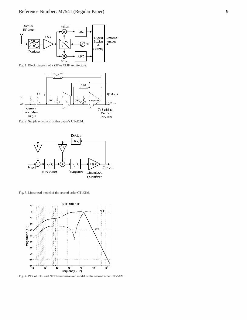
Fig. 9 shows a diagram of the test setup for the probe-able
version. As shown in Fig. 9, the M’s input signal generator
is followed by a low pass filter, which suppresses the signal
generator’s harmonics. The transformer provides impedance
matching between the signal generator and the ’s input.
Capacitors, C3 and C4, are large DC bypass capacitors. The
capacitor, C1b, is the off-chip portion of C1. Resistors, R1a and
R1b, model the mixer’s output impedance and convert the
transformer’s secondary-side voltage to the ’s input
current. To minimize the parasitic impedances between the
’s discrete and integrated circuits, the discrete
components which include, the inductor, L1, the resistors, R1a
and R1b, and the capacitors, C1b, C3, and C4, are mounted on
the tips of the input probes. Another signal generator provides
the ’s clock signal. The ’s single bit output is
buffered by a chain of CML buffers and sent off chip.
Often, the DR or SNR of single bit M can be measured
by sending the ’s output bit stream into a spectrum
analyzer; however, such measurements can be limited by the
bit stream’s noise and any bit stream rising and falling edge
asymmetry caused by the buffers [16][2]. Instead, the ’s
output bit stream is sampled by a high-speed digital
oscilloscope (HSDO) at a rate of 10 GHz. In general, because
the HSDO’s sampling frequency is asynchronous with the
’s sampling frequency, the sampled bit stream’s timing
must be reconstructed. This can be accomplished by
generating an eye diagram from the HSDO’s samples. The
resulting single bit signal was then filtered and decimated.
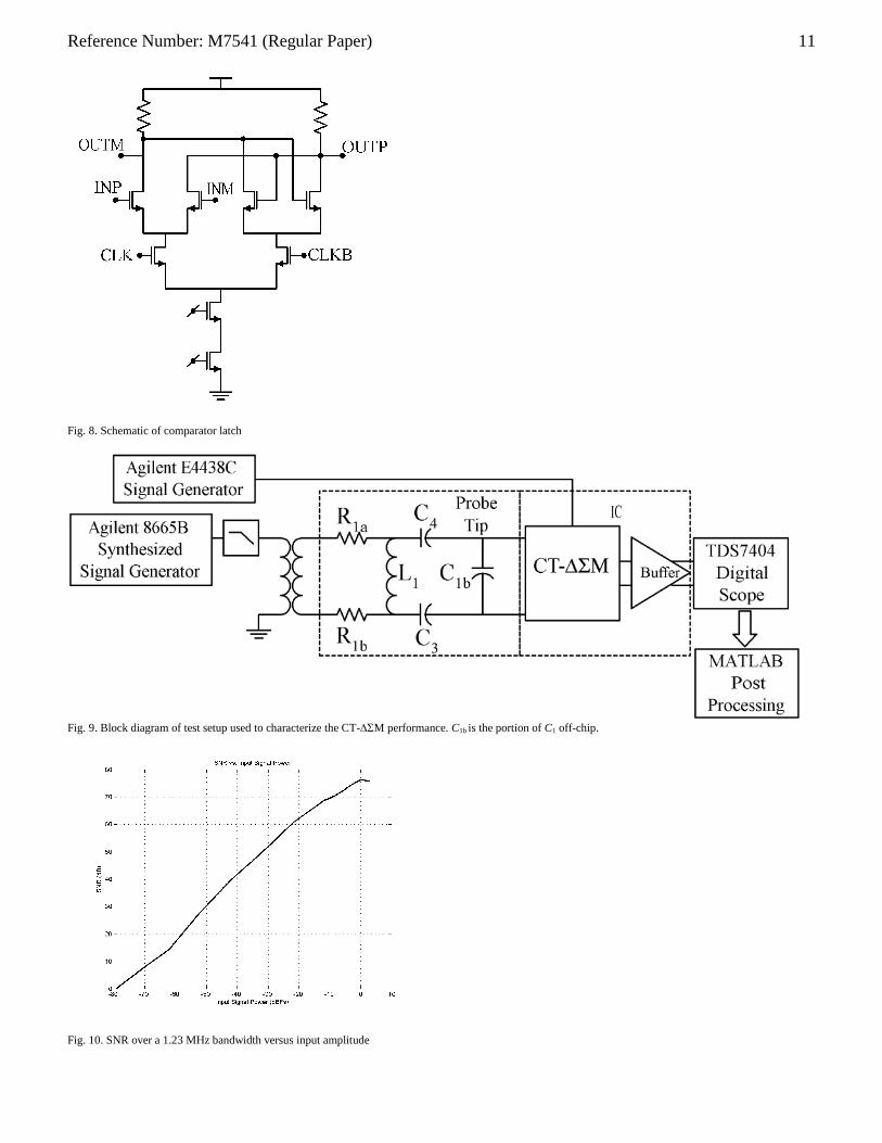
Fig. 10 shows the plot of the ’s measured SNR over a
1.23 MHz bandwidth versus input power for the that has
a 5-latch comparator. This figure shows that the has a
DR of 76.4 dB. Fig. 11 shows the spectral density of a full-
scale input signal after decimation. The SNR shown in Fig. 11
is limited by the signal generator’s close-in phase noise. The
generator’s phase noise could not be suppressed further
because highly linear, narrow band filters at 2.5 MHz were not
available at the time of testing. Fig. 12 shows the
corresponding eye diagram of the single bit output. This
diagram shows that the comparator’s metastability, t, is
approximately 6 ps; however, because the HSDO has a
sampling uncertainty of 6 ps, the comparator’s metastability
could not be measured any more accurately using the HSDO.
Using (12) and the 76.4 dB SNR, it can be shown that the
comparator’s metastability is less than 1.3 ps rms. Fig. 13
shows a power spectral density of a two-tone test to measure
IMP3 suppression or SFDR. The measured IMP3 delta of 69
dB translates to an IIP3 of -1.5 dBm with respect to the
receiver input. This performance meets the earlier derived
specification. Since this requirement includes an allocation to

Reference Number: M7541 (Regular Paper) 7
the duplexer and LNA/mixer this should be sufficient for the
CDMA receiver.
At sampling rates between 1 GHz and a 2 GHz, the 3-latch
performed similarly to the 5-latch ; however, the
two s performed differently at sampling rates below 1
GHz and above 2 GHz. Fig. 14 plots the SNR of the two
Ms as a function of sampling rate. For this plot, the Ms’
inputs are -10 dBFS, and thus, the SNR for a full-scale
sinusoidal input would be 10 dB higher than what is shown.
As shown in Fig. 14, the 3-latch exhibits better
performance at sampling frequencies less than 1 GHz than the
5-latch This result is due to the 3-latch ’s smaller
comparator latency. For example, at a 600 MHz sampling
frequency, the excess loop delay for the 5-latch is 1.1%
of the input signal’s period, and the excess loop delay for the
3-latch is 0.6% of the input signal period. In contrast, at
a 2 GHz sampling frequency, the excess loop delay for a 5-
latch and 3-latch design is 0.4% and 0.2% of the input signal
period, respectively. For sampling frequencies between 1 GHz
and 2 GHz, the SNRs for the 3 and 5-latch s are nearly
equal because the M’s performance is being limited by the
DAC’s device-noise.
As shown in Fig. 14, the 5-latch exhibited better
performance at sampling frequencies above 2 GHz than the 3-
latch because the 5-latch exhibits less metastability
than the 3-latch . The additional 2 latches in the 5-latch
allows the CT-M to maintain consistency in its
feedback waveform at sampling frequencies above 2 GHz.
This allows the 5-latch comparator to meet the metastability
requirement with significant margin.
The performance of the M fabricated as part of a CLIF
receiver was also measured. However, because the was
embedded in the receiver, it was not tested in the same manner
as the M in the standalone probe-able module. The SNR of
the receiver’s M was measured at 79 dB/1.23 MHz which
is 2.6 dB better than the SNR of the standalone module’s
M This improvement is attributed to the receiver’s
improved operating environment, which includes better
grounding, supply by-passing, and improved integration with
the discrete components.
The consumes 10 mA at 1.8 V or 18 mW. Each M
occupies an area of approximately 615 m x 1450 m or
0.892 mm2. Fig. 15 shows a micrograph of the 5-latch CT-
M integrated in a CLIF receiver. 9% of the M’s layout
area consists of the TA, the two DACs, and the comparator.
The integrated portion of capacitor C1, identified as C1a in Fig.
15, and C2 consume another 11% of the area. Supply bypass
capacitors, voltage regulators, and routing used the remaining
80% of the layout area.
VI. CONCLUSION
This paper has presented a CT- fabricated in a standard
CMOS technology. The successful performance of the CT-
in both probe-able and integrated receiver form has
demonstrated that a high speed CMOS CT- modulator
can be constructed with low power consumption, high
dynamic range, and high linearity using basic circuit blocks
and a second order design.
ACKNOWLEDGMENT
The authors greatly appreciate the assistance of B.
Loechner, B. Mann, and J. Saucedo in the intricate probing
and tireless data gathering of the entire CT-. The
discussions and consultations about all aspects of the CT-
with J. Cherry and A. Baschirotto are gratefully
acknowledged.
REFERENCES
[1] D. K. Weaver, “A third method of generation and detection of single-
sideband signals,” Proc. IRE, pp. 1703-5, Dec. 1956. [2] G. Raghavan, J. F. Jensen, J. Laskowski, M. Kardos, M. G. Case, M.
Sokolich, and S. Thomas III, “Architecture, design, and test of
continuous-time tunable intermediate-frequency bandpass delta-sigma modulators,” IEEE J. Solid-State Circuits, vol. 36, no. 1, pp. 5-13, Jan.
2001.
[3] S. Jaganathan, et al., “An 18-GHz continuous-time - analog-digital converter implemented in InP-transferred substrate HBT technology,”
IEEE J. Solid-State Circuits, vol. 36, no. 9, pp. 1343-1350, Sept. 2001.
[4] J. F. Jensen, G. Raghavan, A.E. Coxand, and R. H. Walden, “A 3.2-GHz second-order delta-sigma modulator implemented in InP HBT
techonolgy,” IEEE J. Solid-State Circuits, vol. 30, no. 10, pp 1119-1127,
Oct. 1995. [5] J. A. Cherry, W. M. Snelgrove, W. Gao, “On the design of a forth-order
continuous-time LC delta-sigma modulator for UHF A/D conversion.”
IEEE Trans. on Circuits and Systems II: Analog and Digital Signal Processing, vol. 47, no. 6, pp 518-530, June 2000.
[6] W. Gao, J. A. Cherry, and W. M. Snelgrove, “A 4GHz fourth-order
SiGe HBT band pass modulator,” Symposium on VLSI Circuits Digest of Technical Papers, pp. 174-175, 1998.
[7] M. S. Kappes, “A 2.2-mW CMOS bandpass continuous-time multibit -
ADC with 68 dB of Dynamic Range and 1-MHz bandwidth for wireless applications,” IEEE J. Solid-State Circuits, vol. 38, no. 7, pp
1098-1104, July 2003.
[8] R. van Veldhoven, “A tri-mode continuous-time modulator with switched-capacitor feedback DAC for a GSM-
EDGE/CDMA2000/UMTS receiver,” ISSCC, session 3, Oversampled
A/D Converters, paper 3.4, 2003. [9] TIA/EIA Standard – Recommend Minimum Performance Standards for
cdma2000 Spread Spectrum Mobil Stations, TIA/EIA-98-D-2001,
Telecommunications Industry Association, Jun. 2001. [10] D. A. Johns and K. Martin, Analog Integrated Circuit Design. New
York: John Wiley and Sons, Inc, 1997.
[11] S. R. Norsworthy, R. Schreier, and G. C. Temes, Eds., Delta-Sigma Data Converters – Theory, Design, and Simulation. Piscataway, NJ:
IEEE Press, 1996.
[12] L. Breems and J. H. Huijsing, Continuous-Time Sigma-Delta Modulation for A/D Conversion In Radio Receivers, Boston: Kluwer
Academic Publishers, 2001. [13] J. A. Cherry and W. M. Snelgrove, “Excess loop delay in continuous-
time delta-sigma modulators,” IEEE Trans. Circuits Systems II, vol. 46,
no. 4, pp. 376-389, April 1999. [14] J. A. Cherry and W. M. Snelgrove, Continuous-Time Delta-Sigma
Modulators for High-Speed A/d Conversion: Theory, Practice and
Fundamental Performance Limits, Boston: Kluwer Academic Publishers, 2000.
[15] E. J. van der Zwan and E. C. Dijkmans, “A 0.2-mW CMOS delta-sigma
modulator for speech coding with 80 dB dynamic range,” IEEE J. Solid-State Circuits, vol. 31, pp. 1873-1880, Dec. 1996.
[16] R. W. Adams, “Design and implementation of an audio 18-bit analog-to-
digital converter using oversampling techniques," J. Audio Eng. Soc., vol. 34, no. 3, Mar. 1986.

Reference Number: M7541 (Regular Paper) 8
Elias H. Dagher (S’96–M’00) received the B.S. in
electrical engineering degree, Summa Cum Laude,
from the University of Nevada, Las Vegas in 1998.
He received the M.S. in electrical engineering degree
from Stanford University, Stanford, CA in 1999. In 1997 and 1998, he was an intern with
Rockwell Semiconductor systems where he worked
on circuit simulators and digital design. From 2000 to 2001, he was with Motorola Labs, Schaumburg,
IL, researching dynamic element matching and re-
configurable computing. In 2001, he joined Ditrans Corporation, Irvine, CA, where he designed high-speed data converters and switching power converters
for a digital transceiver. He is now with Skyworks Solutions, Inc., Irvine, CA
working on advanced mixed-signal and power management devices for cellular handsets. His research and work interests include data converter
design, mixed-signal circuit design, digital controls, and modeling.
Peter A. Stubberud received the B.S.E.E., M.S. and
Ph.D. degrees from the University of California, Los
Angeles in 1985, 1987 and 1990, respectively. While attending UCLA, he worked for
Rockwell International, Ford Aerospace, Western
Digital and Hughes Aircraft. After receiving his Ph.D. in Engineering, he continued working for the
Radar Systems Group at Hughes Aircraft until 1991.
In 1991, he became an assistant professor with the Department of Electrical and Computer Engineering
at the University of Nevada Las Vegas (UNLV), and was promoted to associate professor in 1997. During a sabbatical in 2001, he joined Ditrans as
a circuit and systems engineer, and then returned to UNLV in 2002. He has
published over 40 conference and journal papers and several book chapters. His research interests include signal processing, adaptive systems and mixed-
signal circuit design including data converters.
Matteo Conta was born in Pavia, Italy, in 1972. He
received the M.E. degree in electrical engineering,
Summa Cum Laude, from the University of Pavia, Pavia, Italy, in 1996 and the M.B.A. degree from the
University of California, Irvine, in 2002.
From August 1996 to October 2000, he worked as a RF IC design engineer with Conexant
Systems, Newport Beach, CA, where he designed
CMOS frequency synthesizers and phase-locked loops. From October 2000 to October 2002 he was
with Valence Semiconductor, Inc., Irvine, CA, engaging in the design and
development of integrated CMOS transceivers for wireless LAN and GPS. In October 2002, he co-founded RFDomus, where he is currently working on
low power wireless radios. His research interests include the design of RF,
analog, and mixed-signal circuits.
Wesley K. Masenten (M’59, LM’00) received the B.S.E.E. from Purdue University, M.S.E.E. from
Massachusetts Institute of Technology, and Ph.D.
from the University of California, Irvine. He was previously Chief Technical
Officer for Ditrans Corporation where he was
involved in the development of transceivers for wireless communication systems. His prior
associations included: Northrop Corporation, as
Manager of Avionics System Engineering and Hughes Aircraft where he served as Technical Director on spread spectrum
communication and technology programs.
He has served as lecturer in special courses on Spread Spectrum and Interference Rejection Techniques at UCLA, University of Maryland, and
UC Santa Barbara. He has also taught courses in Control Systems, Digital
Control Systems, and Communication Systems at the University of California,
Irvine. He is currently President of Masenten and Associates, a company that
provides consulting services for the design and development of wireless
communication systems.
Thang Victor Dinh received the B.S. degree in
electrical engineering from the University of
California, Irvine, and the M.S. degree in electrical
engineering from the California State University,
Long Beach. From 2000 to 2003, he was at Ditrans
Corporation, Irvine, CA engaged in the development
of a digital transceiver. Currently, he is a design engineer at Unav Microelectronics, Irvine, CA,
engaging in the development of a GPS receiver.
Prior, he was with Tanner Research Inc., Pasadena, CA and Irvine Sensors Corp., Irvine, CA. His research and work interests include mixed-signal
circuit design and ESD design and modeling.
Reference Number: M7541 (Regular Paper) 9
Fig. 1. Block diagram of a ZIF or CLIF architecture.
Fig. 2. Simple schematic of this paper’s CT-M.
Fig. 3. Linearized model of the second order CT-M.
Fig. 4. Plot of STF and NTF from linearized model of the second order CT-M.

Reference Number: M7541 (Regular Paper) 10
Fig. 5. Schematic of TA.
Fig. 6. Schematic of DAC1.
Fig. 7. Block diagram of comparator.
Reference Number: M7541 (Regular Paper) 11
Fig. 8. Schematic of comparator latch
Fig. 9. Block diagram of test setup used to characterize the CT-M performance. C1b is the portion of C1 off-chip.
Fig. 10. SNR over a 1.23 MHz bandwidth versus input amplitude

Reference Number: M7541 (Regular Paper) 12
Fig. 11. Measured power spectral density of probed CT- showing 76.4 dB/1.23 MHz DR. The plot is generated by averaging three 1 K FFTs from the
decimation filter output. The resulting bandwidth resolution is 20 KHz.
Fig. 12. Eye diagram of CT- bit stream. Samples are 100 ps apart.
Fig. 13. Measured power spectral density of a two-tone test showing the IMP3 delta of 69 dB with the 2 tones run at -3 dBFS. The plot is generated by averaging
three 1 K FFTs from the decimation filter output. The resulting bandwidth resolution is 20 KHz.

Reference Number: M7541 (Regular Paper) 13
Fig. 14. SNR over a 1.23 MHz bandwidth versus sampling frequency for the 5-latch and 3-latch comparator implementations of the CT-M. The input signal
power is at -10 dBFS to avoid possible SNR compression that could result from early overloading due to decreased sampling frequency.
Fig. 15. Micrograph of CT- integrated in CLIF receiver. C1a is the portion of C1 integrated on-chip.