Embed Size (px)
Citation preview
VC
C2
4
GN
D2
3
BB
IN2
2
BB
IP2
1
GN
D2
0G
ND
20
GN
D1
9
VCC18
GND17
RF_OUT16
15
14 GND
13
GN
D87
BB
QN
9
BB
QP
10
GN
D11
GN
D1
2
1
2GND
3LOP
4LON
GND 5
6
0/90
S
NC
NC
B0175-01
NC
NC
NC
Product
Folder
Sample &Buy
Technical
Documents
Tools &
Software
Support &Community
TRF370417SLWS213A –JANUARY 2010–REVISED NOVEMBER 2015
TRF370417 50-MHz to 6-GHz Quadrature Modulator1 Features 3 Description
The TRF370417 is a low-noise direct quadrature1• 76-dBc Single-Carrier WCDMA ACPR at –8 dBm
modulator, capable of converting complex modulatedChannel Powersignals from baseband or IF directly up to RF. The
• Low Noise Floor: –162.3 dBm/Hz at 2140 MHz TRF370417 is a high-performance, superior-linearity• OIP3 of 26.5 dBm at 2140 MHz device that operates at RF frequencies of 50 MHz
through 6 GHz. The modulator is implemented as a• P1dB of 12 dBm at 2140 MHzdouble-balanced mixer. The RF output block consists• Carrier Feedthrough of –38 dBm at 2140 MHz of a differential to single-ended converter and an RF
• Side-Band Suppression of –50 dBc at 2140 MHz amplifier capable of driving a single-ended 50-Ω loadwithout any need of external components. The• Single Supply: 4.5-V–5.5-V OperationTRF370417 requires a 1.7-V common-mode voltage• Silicon Germanium Technology for optimum linearity performance.
• 1.7-V CM at I, Q Baseband InputsDevice Information(1)
2 Applications PART NUMBER PACKAGE BODY SIZE (NOM)• Cellular Base Station Transceiver TRF370417 VQFN(24) 4.00 mm × 4.00 mm
• CDMA: IS95, UMTS, CDMA2000, TD-SCDMA (1) For all available packages, see the orderable addendum atthe end of the data sheet.• TDMA: GSM, IS-136, EDGE/UWC-136
• Multicarrier GSM Block Diagram• WiMAX: 802.16d/e• 3GPP: LTE• Point-to-Point (P2P) Microwave• Wideband Software-Defined Radio• Public Safety: TETRA/APC025• Communication-System Testers• Cable Modem Termination System (CMTS)
1
An IMPORTANT NOTICE at the end of this data sheet addresses availability, warranty, changes, use in safety-critical applications,intellectual property matters and other important disclaimers. PRODUCTION DATA.
TRF370417SLWS213A –JANUARY 2010–REVISED NOVEMBER 2015 www.ti.com
Table of Contents7.4 Device Functional Modes........................................ 161 Features .................................................................. 1
8 Application and Implementation ........................ 182 Applications ........................................................... 18.1 Application Information............................................ 183 Description ............................................................. 18.2 Typical Application ................................................. 204 Revision History..................................................... 2
9 Power Supply Recommendations ...................... 235 Pin Configuration and Functions ......................... 310 Layout................................................................... 236 Specifications......................................................... 4
10.1 Layout Guidelines ................................................. 236.1 Absolute Maximum Ratings ...................................... 410.2 Layout Example .................................................... 236.2 ESD Ratings.............................................................. 4
11 Device and Documentation Support ................. 256.3 Recommended Operating Conditions....................... 411.1 Device Support...................................................... 256.4 Thermal Information .................................................. 411.2 Documentation Support ........................................ 266.5 Electrical Characteristics........................................... 511.3 Community Resources.......................................... 266.6 RF Output Parameters.............................................. 511.4 Trademarks ........................................................... 266.7 Typical Characteristics .............................................. 811.5 Electrostatic Discharge Caution............................ 267 Detailed Description ............................................ 1611.6 Glossary ................................................................ 267.1 Overview ................................................................. 16
12 Mechanical, Packaging, and Orderable7.2 Functional Block Diagram ....................................... 16Information ........................................................... 267.3 Feature Description................................................. 16
4 Revision HistoryNOTE: Page numbers for previous revisions may differ from page numbers in the current version.
Changes from Original (January 2010) to Revision A Page
• Added ESD Ratings table, Feature Description section, Device Functional Modes, Application and Implementationsection, Power Supply Recommendations section, Layout section, Device and Documentation Support section, andMechanical, Packaging, and Orderable Information section. ................................................................................................. 1
2 Submit Documentation Feedback Copyright © 2010–2015, Texas Instruments Incorporated
Product Folder Links: TRF370417
GND
RF_OUT
15
14
13
VC
C
GN
D
BB
IN
BB
IP
GN
D
GN
D
24
23
22
21
20
19
GND
1
2
3LOP
4LON
5GND
GN
D
7 8 9B
BQ
N
10 11
BB
QP
GN
D
12
GN
D
18 VCC
17 GND
16
NC
NC
NC
NC
NC 6
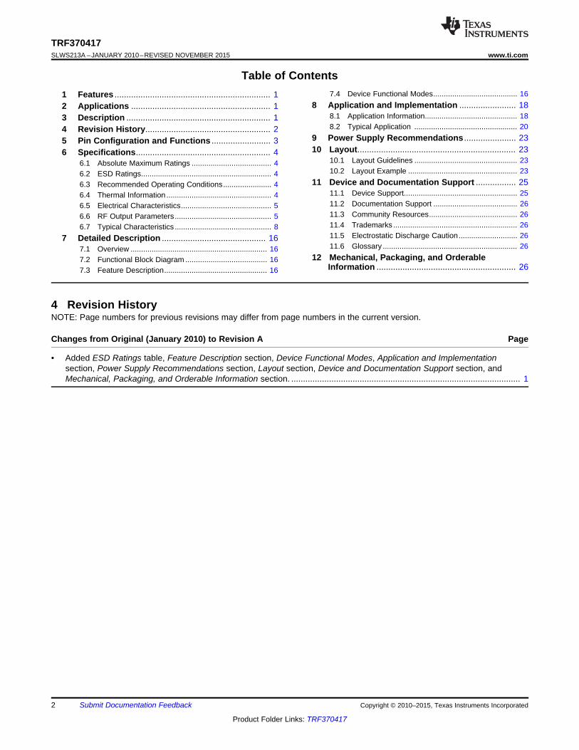
TRF370417www.ti.com SLWS213A –JANUARY 2010–REVISED NOVEMBER 2015
5 Pin Configuration and Functions
RGE Package24-Pin VQFN With Exposed Thermal Pad
Top View
Pin FunctionsPIN
I/O DESCRIPTIONNAME NO.BBIN 22 I In-phase negative inputBBIP 21 I In-phase positive inputBBQN 9 I Quadrature-phase negative inputBBQP 10 I Quadrature-phase positive input
2, 5, 8, 11,GND 12, 14, 17, — Ground
19, 20, 23LON 4 I Local oscillator (LO) negative inputLOP 3 I Local oscillator (LO) positive input
1, 6, 7, 13,NC — No connect15RF_OUT 16 O RF outputVCC 18, 24 — Power supply
Copyright © 2010–2015, Texas Instruments Incorporated Submit Documentation Feedback 3
Product Folder Links: TRF370417
TRF370417SLWS213A –JANUARY 2010–REVISED NOVEMBER 2015 www.ti.com
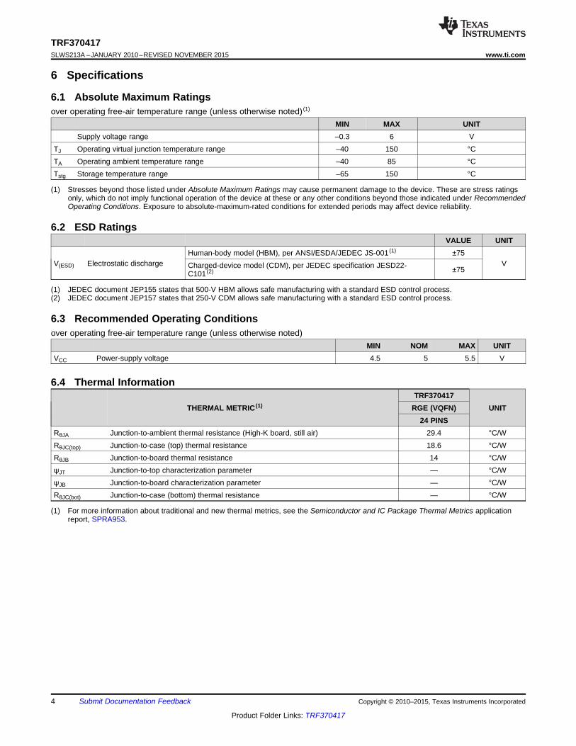
6 Specifications
6.1 Absolute Maximum Ratingsover operating free-air temperature range (unless otherwise noted) (1)
MIN MAX UNITSupply voltage range –0.3 6 V
TJ Operating virtual junction temperature range –40 150 °CTA Operating ambient temperature range –40 85 °CTstg Storage temperature range –65 150 °C
(1) Stresses beyond those listed under Absolute Maximum Ratings may cause permanent damage to the device. These are stress ratingsonly, which do not imply functional operation of the device at these or any other conditions beyond those indicated under RecommendedOperating Conditions. Exposure to absolute-maximum-rated conditions for extended periods may affect device reliability.
6.2 ESD RatingsVALUE UNIT
Human-body model (HBM), per ANSI/ESDA/JEDEC JS-001 (1) ±75V(ESD) Electrostatic discharge VCharged-device model (CDM), per JEDEC specification JESD22- ±75C101 (2)
(1) JEDEC document JEP155 states that 500-V HBM allows safe manufacturing with a standard ESD control process.(2) JEDEC document JEP157 states that 250-V CDM allows safe manufacturing with a standard ESD control process.
6.3 Recommended Operating Conditionsover operating free-air temperature range (unless otherwise noted)
MIN NOM MAX UNITVCC Power-supply voltage 4.5 5 5.5 V
6.4 Thermal InformationTRF370417
THERMAL METRIC (1) RGE (VQFN) UNIT24 PINS
RθJA Junction-to-ambient thermal resistance (High-K board, still air) 29.4 °C/WRθJC(top) Junction-to-case (top) thermal resistance 18.6 °C/WRθJB Junction-to-board thermal resistance 14 °C/WψJT Junction-to-top characterization parameter — °C/WψJB Junction-to-board characterization parameter — °C/WRθJC(bot) Junction-to-case (bottom) thermal resistance — °C/W
(1) For more information about traditional and new thermal metrics, see the Semiconductor and IC Package Thermal Metrics applicationreport, SPRA953.
4 Submit Documentation Feedback Copyright © 2010–2015, Texas Instruments Incorporated
Product Folder Links: TRF370417
TRF370417www.ti.com SLWS213A –JANUARY 2010–REVISED NOVEMBER 2015
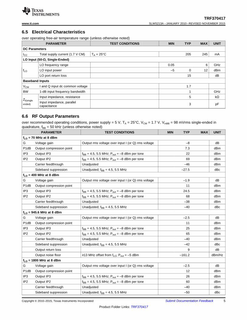
6.5 Electrical Characteristicsover operating free-air temperature range (unless otherwise noted)
PARAMETER TEST CONDITIONS MIN TYP MAX UNITDC ParametersICC Total supply current (1.7 V CM) TA = 25°C 205 245 mALO Input (50-Ω, Single-Ended)
LO frequency range 0.05 6 GHzfLO LO input power –5 0 12 dBm
LO port return loss 15 dBBaseband InputsVCM I and Q input dc common voltage 1.7BW 1-dB input frequency bandwidth 1 GHz
Input impedance, resistance 5 kΩZI(single Input impedance, parallelended) 3 pFcapacitance
6.6 RF Output Parametersover recommended operating conditions, power supply = 5 V, TA = 25°C, VCM = 1.7 V, VinBB = 98 mVrms single-ended inquadrature, fBB = 50 kHz (unless otherwise noted)
PARAMETER TEST CONDITIONS MIN TYP MAX UNITfLO = 70 MHz at 8 dBmG Voltage gain Output rms voltage over input I (or Q) rms voltage –8 dBP1dB Output compression point 7.3 dBmIP3 Output IP3 fBB = 4.5, 5.5 MHz; Pout = –8 dBm per tone 22 dBmIP2 Output IP2 fBB = 4.5, 5.5 MHz; Pout = –8 dBm per tone 69 dBm
Carrier feedthrough Unadjusted –46 dBmSideband suppression Unadjusted; fBB = 4.5, 5.5 MHz –27.5 dBc
fLO = 400 MHz at 8 dBmG Voltage gain Output rms voltage over input I (or Q) rms voltage –1.9 dBP1dB Output compression point 11 dBmIP3 Output IP3 fBB = 4.5, 5.5 MHz; Pout = –8 dBm per tone 24.5 dBmIP2 Output IP2 fBB = 4.5, 5.5 MHz; Pout = –8 dBm per tone 68 dBm
Carrier feedthrough Unadjusted –38 dBmSideband suppression Unadjusted; fBB = 4.5, 5.5 MHz –40 dBc
fLO = 945.6 MHz at 8 dBmG Voltage gain Output rms voltage over input I (or Q) rms voltage –2.5 dBP1dB Output compression point 11 dBmIP3 Output IP3 fBB = 4.5, 5.5 MHz; Pout = –8 dBm per tone 25 dBmIP2 Output IP2 fBB = 4.5, 5.5 MHz; Pout = –8 dBm per tone 65 dBm
Carrier feedthrough Unadjusted –40 dBmSideband suppression Unadjusted; fBB = 4.5, 5.5 MHz –42 dBcOutput return loss 9 dBOutput noise floor ≥13 MHz offset from fLO; Pout = –5 dBm –161.2 dBm/Hz
fLO = 1800 MHz at 8 dBmG Voltage gain Output rms voltage over input I (or Q) rms voltage –2.5 dBP1dB Output compression point 12 dBmIP3 Output IP3 fBB = 4.5, 5.5 MHz; Pout = –8 dBm per tone 26 dBmIP2 Output IP2 fBB = 4.5, 5.5 MHz; Pout = –8 dBm per tone 60 dBm
Carrier feedthrough Unadjusted –40 dBmSideband suppression Unadjusted; fBB = 4.5, 5.5 MHz –50 dBc
Copyright © 2010–2015, Texas Instruments Incorporated Submit Documentation Feedback 5
Product Folder Links: TRF370417
TRF370417SLWS213A –JANUARY 2010–REVISED NOVEMBER 2015 www.ti.com
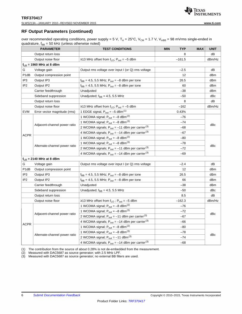
RF Output Parameters (continued)over recommended operating conditions, power supply = 5 V, TA = 25°C, VCM = 1.7 V, VinBB = 98 mVrms single-ended inquadrature, fBB = 50 kHz (unless otherwise noted)
PARAMETER TEST CONDITIONS MIN TYP MAX UNITOutput return loss 8 dBOutput noise floor ≥13 MHz offset from fLO; Pout = –5 dBm –161.5 dBm/Hz
fLO = 1960 MHz at 8 dBmG Voltage gain Output rms voltage over input I (or Q) rms voltage –2.5 dBP1dB Output compression point 12 dBmIP3 Output IP3 fBB = 4.5, 5.5 MHz; Pout = –8 dBm per tone 26.5 dBmIP2 Output IP2 fBB = 4.5, 5.5 MHz; Pout = –8 dBm per tone 60 dBm
Carrier feedthrough Unadjusted –38 dBmSideband suppression Unadjusted; fBB = 4.5, 5.5 MHz –50 dBcOutput return loss 8 dBOutput noise floor ≥13 MHz offset from fLO; Pout = –5 dBm –162 dBm/Hz
EVM Error vector magnitude (rms) 1 EDGE signal, Pout = –5 dBm (1) 0.43%1 WCDMA signal; Pout = –8 dBm (2) –761 WCDMA signal; Pout = –8 dBm (3) –74
Adjacent-channel power ratio dBc2 WCDMA signals; Pout = –11 dBm per carrier (3) –684 WCDMA signals; Pout = –14 dBm per carrier (3) –67
ACPR1 WCDMA signal; Pout = –8 dBm (2) –801 WCDMA signal; Pout = –8 dBm (3) –78
Alternate-channel power ratio dBc2 WCDMA signals; Pout = –11 dBm per carrier (3) –724 WCDMA signals; Pout = –14 dBm per carrier (3) –69
fLO = 2140 MHz at 8 dBmG Voltage gain Output rms voltage over input I (or Q) rms voltage –2.4 dBP1dB Output compression point 12 dBmIP3 Output IP3 fBB = 4.5, 5.5 MHz; Pout = –8 dBm per tone 26.5 dBmIP2 Output IP2 fBB = 4.5, 5.5 MHz; Pout = –8 dBm per tone 66 dBm
Carrier feedthrough Unadjusted –38 dBmSideband suppression Unadjusted; fBB = 4.5, 5.5 MHz –50 dBcOutput return loss 8.5 dBOutput noise floor ≥13 MHz offset from fLO ; Pout = –5 dBm –162.3 dBm/Hz
1 WCDMA signal; Pout = –8 dBm (2) –761 WCDMA signal; Pout = –8 dBm (3) –72
Adjacent-channel power ratio dBc2 WCDMA signal; Pout = –11 dBm per carrier (3) –674 WCDMA signals; Pout = –14 dBm per carrier (3) –66
ACPR1 WCDMA signal; Pout = –8 dBm (2) –801 WCDMA signal; Pout = –8 dBm (3) –78
Alternate-channel power ratio dBc2 WCDMA signal; Pout = –11 dBm (3) –744 WCDMA signals; Pout = –14 dBm per carrier (3) –68
(1) The contribution from the source of about 0.28% is not de-embedded from the measurement.(2) Measured with DAC5687 as source generator; with 2.5 MHz LPF.(3) Measured with DAC5687 as source generator; no external BB filters are used.
6 Submit Documentation Feedback Copyright © 2010–2015, Texas Instruments Incorporated
Product Folder Links: TRF370417
TRF370417www.ti.com SLWS213A –JANUARY 2010–REVISED NOVEMBER 2015
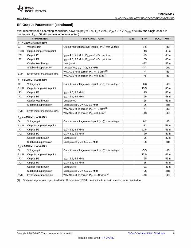
RF Output Parameters (continued)over recommended operating conditions, power supply = 5 V, TA = 25°C, VCM = 1.7 V, VinBB = 98 mVrms single-ended inquadrature, fBB = 50 kHz (unless otherwise noted)
PARAMETER TEST CONDITIONS MIN TYP MAX UNITfLO = 2500 MHz at 8 dBmG Voltage gain Output rms voltage over input I (or Q) rms voltage –1.6 dBP1dB Output compression point 13 dBmIP3 Output IP3 fBB = 4.5, 5.5 MHz; Pout = –8 dBm per tone 29 dBmIP2 Output IP2 fBB = 4.5, 5.5 MHz; Pout = –8 dBm per tone 65 dBm
Carrier feedthrough Unadjusted –37 dBmSideband suppression Unadjusted; fBB = 4.5, 5.5 MHz –47 dBc
WiMAX 5-MHz carrier, Pout = –8 dBm (4) –47 dBEVM Error vector magnitude (rms)
WiMAX 5-MHz carrier, Pout = 0 dBm (4) –45 dBfLO = 3500 MHz at 8 dBmG Voltage gain Output rms voltage over input I (or Q) rms voltage 0.6 dBP1dB Output compression point 13.5 dBmIP3 Output IP3 fBB = 4.5, 5.5 MHz 25 dBmIP2 Output IP2 fBB = 4.5, 5.5 MHz 65 dBm
Carrier feedthrough Unadjusted –35 dBmSideband suppression Unadjusted; fBB = 4.5, 5.5 MHz –36 dBc
WiMAX 5-MHz carrier, Pout = –8 dBm (4) –47 dBEVM Error vector magnitude (rms)
WiMAX 5-MHz carrier, Pout = 0 dBm (4) –43 dBfLO = 4000 MHz at 8 dBmG Voltage gain Output rms voltage over input I (or Q) rms voltage 0.2 dBP1dB Output compression point 12 dBmIP3 Output IP3 fBB = 4.5, 5.5 MHz 22.5 dBmIP2 Output IP2 fBB = 4.5, 5.5 MHz 60 dBm
Carrier feedthrough Unadjusted –36 dBmSideband suppression Unadjusted; fBB = 4.5, 5.5 MHz –36 dBc
fLO = 5800 MHz at 4 dBmG Voltage gain Output rms voltage over input I (or Q) rms voltage –5.5 dBP1dB Output compression point 12.9 dBmIP3 Output IP3 fBB = 4.5, 5.5 MHz 25 dBmIP2 Output IP2 fBB = 4.5, 5.5 MHz 55 dBm
Carrier feedthrough Unadjusted –31 dBmSideband suppression Unadjusted; fBB = 4.5, 5.5 MHz –36 dBc
EVM Error-vector magnitude WiMAX 5-MHz carrier, Pout = –12 dBm (4) –40 dB
(4) Sideband suppression optimized with LO drive level; EVM contribution from instrument is not accounted for.
Copyright © 2010–2015, Texas Instruments Incorporated Submit Documentation Feedback 7
Product Folder Links: TRF370417
f − Frequency − MHz
4
6
8
10
12
14
16
18
20
0 1000 2000 3000 4000 5000 6000
P1d
B −
dB
m
G005
–40°C
25°C
LO = 4 dBmVCC = 5 V
85°C
f − Frequency − MHz
4
6
8
10
12
14
16
18
20
0 1000 2000 3000 4000 5000 6000
P1d
B −
dB
m
G006
4.5 V
5.5 V
5 V
LO = 4 dBmTA = 25°C
f − Frequency − MHz
−12
−10
−8
−6
−4
−2
0
2
0 1000 2000 3000 4000 5000 6000
PO
UT −
Out
put P
ower
− d
Bm
G003
VIN = 98 mVrms SELO = 4 dBmTA = 25°C
4.5 V
5 V
5.5 V
f − Frequency − MHz
−12
−10
−8
−6
−4
−2
0
2
0 1000 2000 3000 4000 5000 6000
PO
UT −
Out
put P
ower
− d
Bm
G004
VIN = 98 mVrms SEVCC = 5 VTA = 25°C
–5 dBm
0 dBm
4 dBm
8 dBm
−20
−15
−10
−5
0
5
10
15
VBB − Baseband Voltage Single-Ended RMS − V
PO
UT −
Out
put P
ower
at 2
.14
GH
z −
dBm
0.01 0.1 1
G001f − Frequency − MHz
−12
−10
−8
−6
−4
−2
0
2
0 1000 2000 3000 4000 5000 6000
PO
UT −
Out
put P
ower
− d
Bm
G002
–40°C
25°C
85°C
VIN = 98 mVrms SELO = 4 dBmVCC = 5 V
TRF370417SLWS213A –JANUARY 2010–REVISED NOVEMBER 2015 www.ti.com
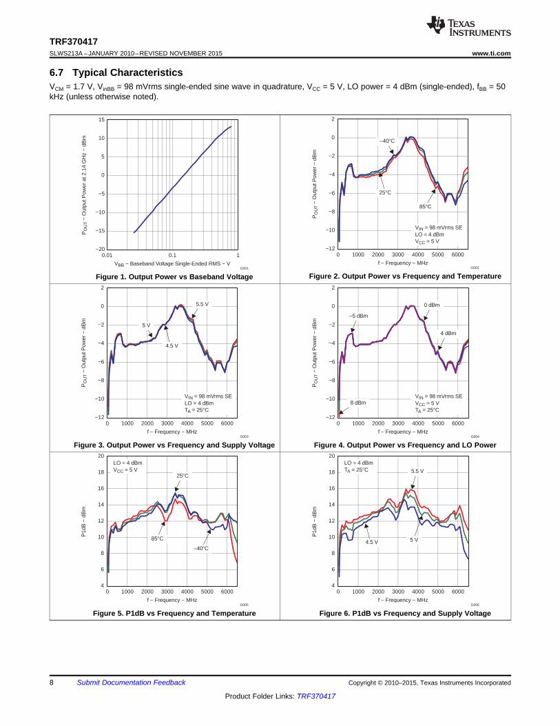
6.7 Typical CharacteristicsVCM = 1.7 V, VinBB = 98 mVrms single-ended sine wave in quadrature, VCC = 5 V, LO power = 4 dBm (single-ended), fBB = 50kHz (unless otherwise noted).
Figure 2. Output Power vs Frequency and TemperatureFigure 1. Output Power vs Baseband Voltage
Figure 3. Output Power vs Frequency and Supply Voltage Figure 4. Output Power vs Frequency and LO Power
Figure 5. P1dB vs Frequency and Temperature Figure 6. P1dB vs Frequency and Supply Voltage
8 Submit Documentation Feedback Copyright © 2010–2015, Texas Instruments Incorporated
Product Folder Links: TRF370417
f − Frequency − MHz
20
30
40
50
60
70
80
90
100
0 1000 2000 3000 4000 5000 6000
OIP
2 −
dBm
G012
4.5 V
5.5 V
5 V
fBB = 4.5, 5.5 MHzPOUT = −8 dBm Per ToneLO = 4 dBmTA = 25°C
20
30
40
50
60
70
80
90
100
0 1000 2000 3000 4000 5000 6000
f − Frequency − MHz
OIP
2 −
dBm
G013
–5 dBm
fBB = 4.5, 5.5 MHzPOUT = −8 dBm Per ToneVCC = 5 VTA = 25°C
4 dBm
8 dBm
0 dBm
f − Frequency − MHz
5
10
15
20
25
30
35
40
0 1000 2000 3000 4000 5000 6000
OIP
3 −
dBm
G009
5 V
4.5 V5.5 V
fBB = 4.5, 5.5 MHzPOUT = −8 dBm Per ToneLO = 4 dBmTA = 25°C
20
30
40
50
60
70
80
90
100
0 1000 2000 3000 4000 5000 6000
f − Frequency − MHz
OIP
2 −
dBm
G011
–40°C 25°C
85°C
fBB = 4.5, 5.5 MHzPOUT = −8 dBm Per ToneLO = 4 dBmVCC = 5 V
f − Frequency − MHz
0
5
10
15
20
25
30
35
40
0 1000 2000 3000 4000 5000 6000
OIP
3 −
dBm
G008
fBB = 4.5, 5.5 MHzPOUT = −8 dBm Per ToneLO = 4 dBmVCC = 5 V
–40°C25°C
85°C
f − Frequency − MHz
0
2
4
6
8
10
12
14
16
18
20
0 1000 2000 3000 4000 5000 6000
P1d
B −
dB
m
G007
–5 dBm
VCC = 5 VTA = 25°C
0 dBm
4 dBm
8 dBm
TRF370417www.ti.com SLWS213A –JANUARY 2010–REVISED NOVEMBER 2015
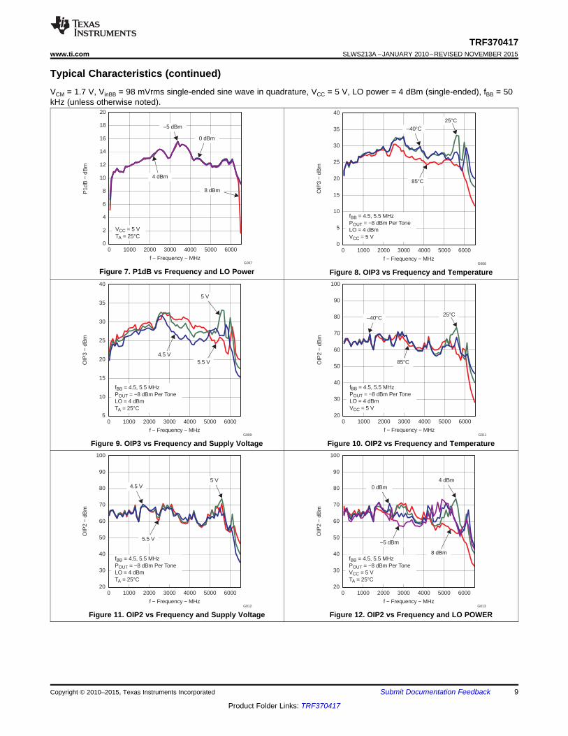
Typical Characteristics (continued)VCM = 1.7 V, VinBB = 98 mVrms single-ended sine wave in quadrature, VCC = 5 V, LO power = 4 dBm (single-ended), fBB = 50kHz (unless otherwise noted).
Figure 7. P1dB vs Frequency and LO Power Figure 8. OIP3 vs Frequency and Temperature
Figure 9. OIP3 vs Frequency and Supply Voltage Figure 10. OIP2 vs Frequency and Temperature
Figure 11. OIP2 vs Frequency and Supply Voltage Figure 12. OIP2 vs Frequency and LO POWER
Copyright © 2010–2015, Texas Instruments Incorporated Submit Documentation Feedback 9
Product Folder Links: TRF370417
f − Frequency − MHz
−80
−70
−60
−50
−40
−30
−20
−10
0
0 1000 2000 3000 4000 5000 6000
SS
− U
nadj
uste
d S
ideb
and
Sup
pres
sion
− d
Bc
G018
LO = 4 dBmTA = 25°C
5.5 V
4.5 V
5 V
f − Frequency − MHz
−80
−70
−60
−50
−40
−30
−20
−10
0
0 1000 2000 3000 4000 5000 6000
SS
− U
nadj
usre
d S
ideb
and
Sup
pres
sion
− d
Bc
G019
VCC = 5 VTA = 25°C
–5 dBm
0 dBm
8 dBm
4 dBm
f − Frequency − MHz
−60
−50
−40
−30
−20
−10
0
0 1000 2000 3000 4000 5000 6000
CS
− U
nadj
uste
d C
arrie
r F
eedt
hrou
gh −
dB
m
G016
VCC = 5 VTA = 25°C
0 dBm
8 dBm
4 dBm
–5 dBm
f − Frequency − MHz
−80
−70
−60
−50
−40
−30
−20
−10
0
0 1000 2000 3000 4000 5000 6000
SS
− U
nadj
uste
d S
ideb
and
Sup
pres
sion
− d
Bc
G017
LO = 4 dBmVCC = 5 V
85°C
25°C
–40°C
f − Frequency − MHz
−80
−70
−60
−50
−40
−30
−20
−10
0
0 1000 2000 3000 4000 5000 6000
CS
− U
nadj
uste
d C
arrie
r F
eedt
hrou
gh −
dB
m
G014
LO = 4 dBmVCC = 5 V
–40°C
85°C
25°C
f − Frequency − MHz
−80
−70
−60
−50
−40
−30
−20
−10
0
0 1000 2000 3000 4000 5000 6000
CS
− U
nadj
uste
d C
arrie
r F
eedt
hrou
gh −
dB
m
G015
LO = 4 dBmTA = 25°C
5.5 V
5 V
4.5 V
TRF370417SLWS213A –JANUARY 2010–REVISED NOVEMBER 2015 www.ti.com
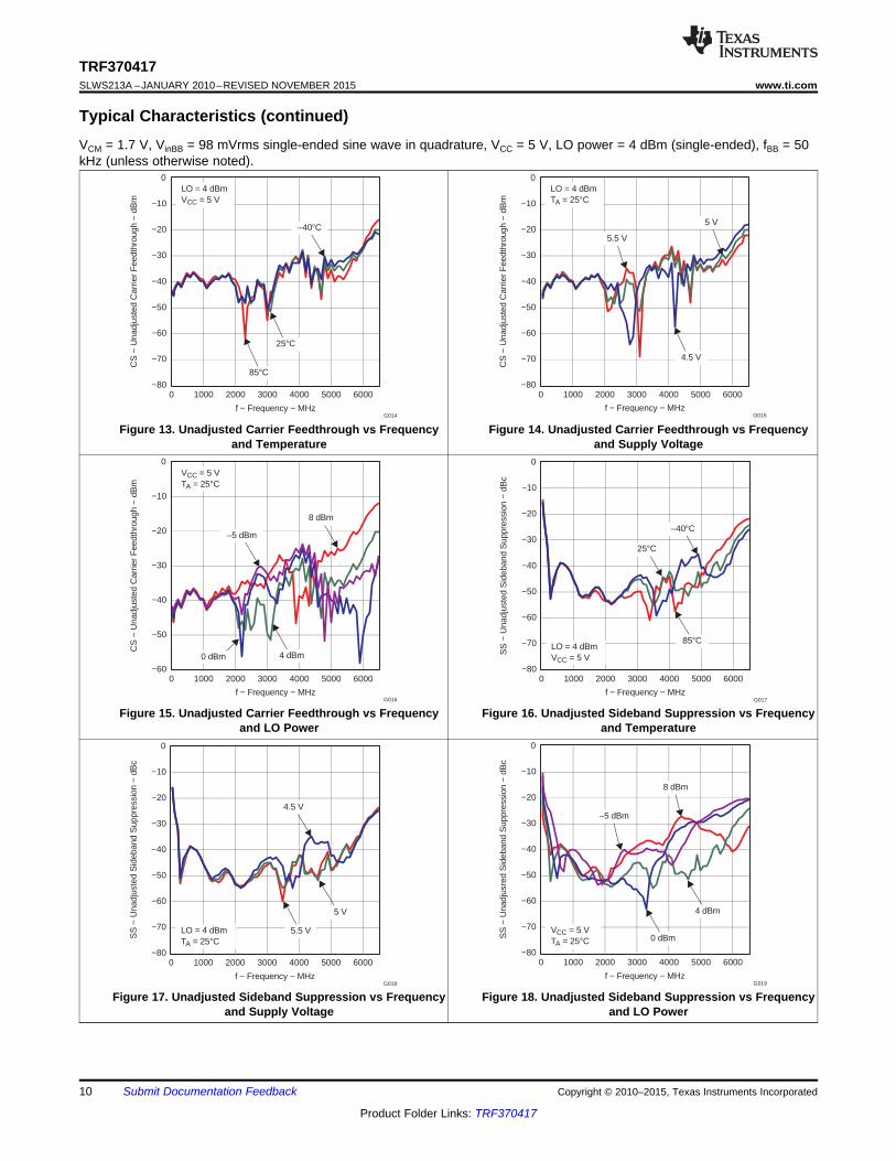
Typical Characteristics (continued)VCM = 1.7 V, VinBB = 98 mVrms single-ended sine wave in quadrature, VCC = 5 V, LO power = 4 dBm (single-ended), fBB = 50kHz (unless otherwise noted).
Figure 13. Unadjusted Carrier Feedthrough vs Frequency Figure 14. Unadjusted Carrier Feedthrough vs Frequencyand Temperature and Supply Voltage
Figure 15. Unadjusted Carrier Feedthrough vs Frequency Figure 16. Unadjusted Sideband Suppression vs Frequencyand LO Power and Temperature
Figure 17. Unadjusted Sideband Suppression vs Frequency Figure 18. Unadjusted Sideband Suppression vs Frequencyand Supply Voltage and LO Power
10 Submit Documentation Feedback Copyright © 2010–2015, Texas Instruments Incorporated
Product Folder Links: TRF370417
−80
−70
−60
−50
−40
−30
−20
−10
0
2040 2080 2120 2160 2200 2240
f − Frequency − MHz
CS
− A
djus
ted
Car
rier
Fee
dthr
ough
− d
Bm
G025
85°C–40°C
25°C
Adj at 2140 MHz @ 25°CLO = 4 dBmVCC = 5 V
−80
−70
−60
−50
−40
−30
−20
−10
0
900 910 920 930 940 950 960 970 980 990 1000
f − Frequency − MHz
CS
− A
djus
ted
Car
rier
Fee
dthr
ough
− d
Bm
G024
85°C
–40°C25°C
Adj at 942.6 MHz @ 25°CLO = 4 dBmVCC = 5 V
POUT − Output Power − dBm
−166
−164
−162
−160
−158
−156
−154
−10−9 −8 −7 −6 −5 −4 −3 −2 −1 0 1 2 3 4 5
Noi
se a
t 13-
MH
z O
ffset
− d
Bm
/Hz
G022
948.5 MHz
VCC = 5 VLO = 8 dBmTA = 25°C
1960 MHz
1800 MHz
2140 MHz
5600 MHz
−80
−70
−60
−50
−40
−30
−20
−10
0
60 62 64 66 68 70 72 74 76 78 80
f − Frequency − MHz
CS
− A
djus
ted
Car
rier
Fee
dthr
ough
− d
Bm
G023
Adj at 70 MHz @ 25°CLO = 4 dBmVCC = 5 V
–40°C
85°C25°C
f − Frequency − GHz
−170
−168
−166
−164
−162
−160
−158
−156
−154
−152
−150
0.8 1.4 2.0 2.6 3.2 3.8 4.4 5.0 5.6
Noi
se a
t 13-
MH
z O
ffset
− d
Bm
/Hz
G020
–40°C25°C
POUT = −5 dBmLO = 8 dBmVCC = 5 V
85°C
f − Frequency − GHz
−170
−168
−166
−164
−162
−160
−158
−156
−154
−152
−150
0.8 1.4 2.0 2.6 3.2 3.8 4.4 5.0 5.6
Noi
se a
t 13-
MH
z O
ffset
− d
Bm
/Hz
G021
5.5 V
POUT = −5 dBmLO = 8 dBmTA = 25°C
4.5 V5 V
TRF370417www.ti.com SLWS213A –JANUARY 2010–REVISED NOVEMBER 2015
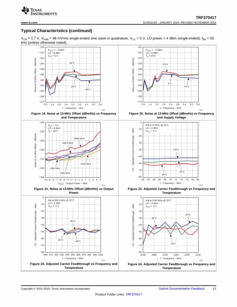
Typical Characteristics (continued)VCM = 1.7 V, VinBB = 98 mVrms single-ended sine wave in quadrature, VCC = 5 V, LO power = 4 dBm (single-ended), fBB = 50kHz (unless otherwise noted).
Figure 19. Noise at 13-MHz Offset (dBm/Hz) vs Frequency Figure 20. Noise at 13-MHz Offset (dBm/Hz) vs Frequencyand Temperature and Supply Voltage
Figure 21. Noise at 13-MHz Offset (dBm/Hz) vs Output Figure 22. Adjusted Carrier Feedthrough vs Frequency andPower Temperature
Figure 23. Adjusted Carrier Feedthrough vs Frequency and Figure 24. Adjusted Carrier Feedthrough vs Frequency andTemperature Temperature
Copyright © 2010–2015, Texas Instruments Incorporated Submit Documentation Feedback 11
Product Folder Links: TRF370417
−80
−70
−60
−50
−40
−30
−20
−10
0
900 910 920 930 940 950 960 970 980 990 1000
f − Frequency − MHz
SS
− A
djus
ted
Sid
eban
d S
uppr
essi
on −
dB
c
G030
85°C
–40°C
25°C
Adj at 942.6 MHz @ 25°CLO = 4 dBmVCC = 5 V
−80
−70
−60
−50
−40
−30
−20
−10
0
2040 2080 2120 2160 2200 2240
f − Frequency − MHz
SS
− A
djus
ted
Sid
eban
d S
uppr
essi
on −
dB
c
G031
–40°C85°C
25°C
Adj at 2140 MHz @ 25°CLO = 4 dBmVCC = 5 V
−80
−70
−60
−50
−40
−30
−20
−10
0
5700 5740 5780 5820 5860 5900
f − Frequency − MHz
CS
− A
djus
ted
Car
rier
Fee
dthr
ough
− d
Bm
G028
–40°C
25°C85°C
Adj at 5800 MHz @ 25°CLO = 4 dBmVCC = 5 V
−80
−70
−60
−50
−40
−30
−20
−10
0
60 62 64 66 68 70 72 74 76 78 80
f − Frequency − MHz
SS
− A
djus
ted
Sid
eban
d S
uppr
essi
on −
dB
c
G029
–40°C25°C
85°C
Adj at 70 MHz @ 25°CLO = 4 dBmVCC = 5 V
−80
−70
−60
−50
−40
−30
−20
−10
0
2400 2440 2480 2520 2560 2600
f − Frequency − MHz
CS
− A
djus
ted
Car
rier
Fee
dthr
ough
− d
Bm
G026
85°C
–40°C
25°C
Adj at 2500 MHz @ 25°CLO = 4 dBmVCC = 5 V
−80
−70
−60
−50
−40
−30
−20
−10
0
3400 3440 3480 3520 3560 3600
f − Frequency − MHz
CS
− A
djus
ted
Car
rier
Fee
dthr
ough
− d
Bm
G027
–40°C
25°C85°C
Adj at 3500 MHz @ 25°CLO = 4 dBmVCC = 5 V
TRF370417SLWS213A –JANUARY 2010–REVISED NOVEMBER 2015 www.ti.com
Typical Characteristics (continued)VCM = 1.7 V, VinBB = 98 mVrms single-ended sine wave in quadrature, VCC = 5 V, LO power = 4 dBm (single-ended), fBB = 50kHz (unless otherwise noted).
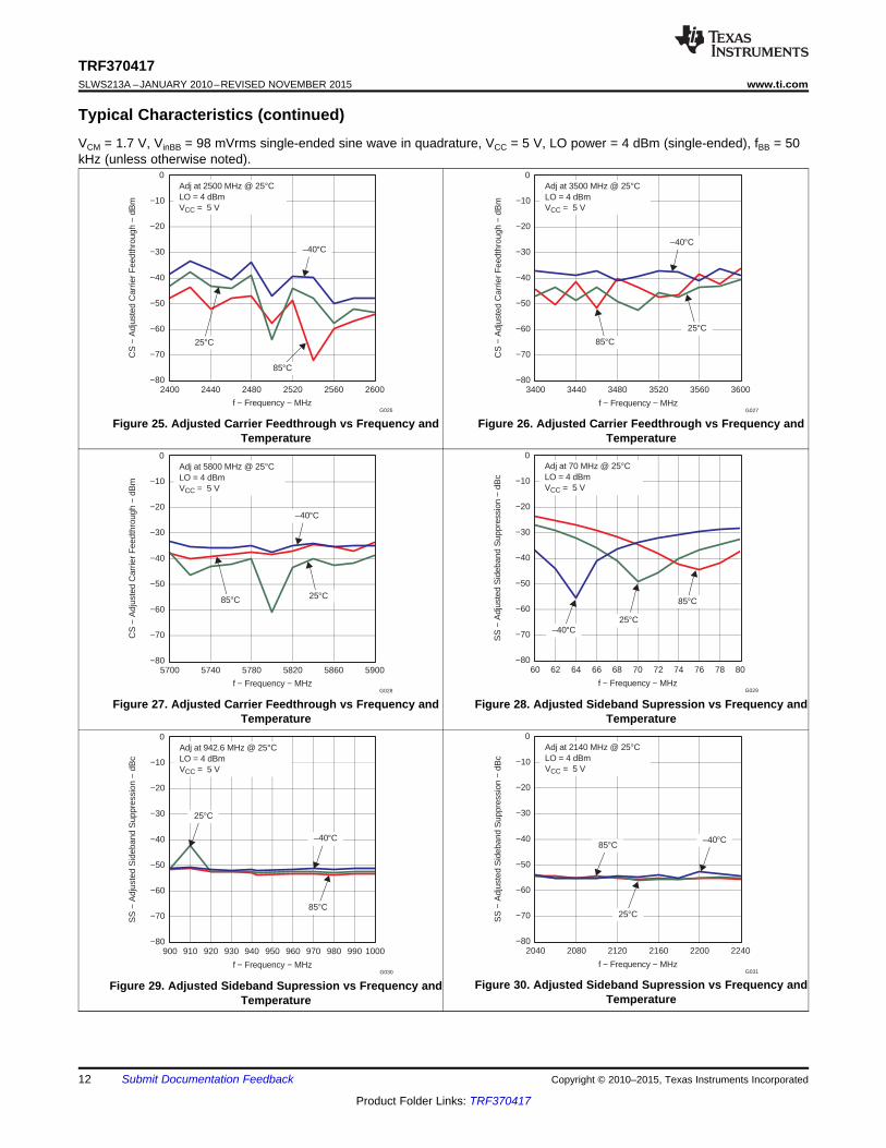
Figure 25. Adjusted Carrier Feedthrough vs Frequency and Figure 26. Adjusted Carrier Feedthrough vs Frequency andTemperature Temperature
Figure 27. Adjusted Carrier Feedthrough vs Frequency and Figure 28. Adjusted Sideband Supression vs Frequency andTemperature Temperature
Figure 30. Adjusted Sideband Supression vs Frequency andFigure 29. Adjusted Sideband Supression vs Frequency andTemperatureTemperature
12 Submit Documentation Feedback Copyright © 2010–2015, Texas Instruments Incorporated
Product Folder Links: TRF370417
10
13
16
19
22
25
28
31
34
37
40
1.40 1.45 1.50 1.55 1.60 1.65 1.70 1.75 1.80
VCM − Common-Mode Voltage − V
OIP
3 −
dBm
G037
fBB = 4.5, 5.5 MHzPOUT = −8 dBm Per ToneLO = 4 dBmVCC = 5 V
25°C
–40°C 85°C
10
12
14
16
18
20
22
24
26
28
30
32
1.40 1.45 1.50 1.55 1.60 1.65 1.70 1.75 1.80
VCM − Common-Mode Voltage − V
OIP
3 −
dBm
G036
fBB = 4.5, 5.5 MHzPOUT = −8 dBm Per ToneLO = 4 dBmVCC = 5 V
25°C
–40°C
85°C
−80
−70
−60
−50
−40
−30
−20
−10
0
5700 5740 5780 5820 5860 5900
f − Frequency − MHz
SS
− A
djus
ted
Sid
eban
d S
uppr
essi
on −
dB
c
G034
25°C
–40°C
85°C
Adj at 5800 MHz @ 25°CLO = 4 dBmVCC = 5 V
10
12
14
16
18
20
22
24
26
28
30
1.40 1.45 1.50 1.55 1.60 1.65 1.70 1.75 1.80
VCM − Common-Mode Voltage − V
OIP
3 −
dBm
G035
fBB = 4.5, 5.5 MHzPOUT = −8 dBm Per ToneLO = 4 dBmVCC = 5 V
25°C
–40°C
85°C
−80
−70
−60
−50
−40
−30
−20
−10
0
2400 2440 2480 2520 2560 2600
f − Frequency − MHz
SS
− A
djus
ted
Sid
eban
d S
uppr
essi
on −
dB
c
G032
25°C
–40°C
85°C
Adj at 2500 MHz @ 25°CLO = 4 dBmVCC = 5 V
−80
−70
−60
−50
−40
−30
−20
−10
0
3400 3440 3480 3520 3560 3600
f − Frequency − MHz
SS
− A
djus
ted
Sid
eban
d S
uppr
essi
on −
dB
c
G033
25°C
–40°C
85°C
Adj at 3500 MHz @ 25°CLO = 4 dBmVCC = 5 V
TRF370417www.ti.com SLWS213A –JANUARY 2010–REVISED NOVEMBER 2015
Typical Characteristics (continued)VCM = 1.7 V, VinBB = 98 mVrms single-ended sine wave in quadrature, VCC = 5 V, LO power = 4 dBm (single-ended), fBB = 50kHz (unless otherwise noted).
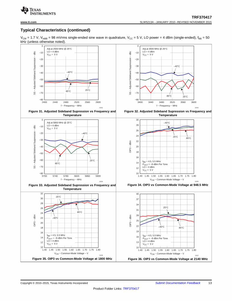
Figure 31. Adjusted Sideband Supression vs Frequency and Figure 32. Adjusted Sideband Supression vs Frequency andTemperature Temperature
Figure 34. OIP3 vs Common-Mode Voltage at 948.5 MHzFigure 33. Adjusted Sideband Supression vs Frequency andTemperature
Figure 35. OIP3 vs Common-Mode Voltage at 1800 MHz Figure 36. OIP3 vs Common-Mode Voltage at 2140 MHz
Copyright © 2010–2015, Texas Instruments Incorporated Submit Documentation Feedback 13
Product Folder Links: TRF370417
CS − Unadjusted Carrier Feedthrough − dBm
0
2
4
6
8
10
12
14
16
18
−24 −28 −32 −36 −40 −44 −48 −52 −56 −60 −64
Dis
trib
utio
n −
%
G044SS − Unadjusted Sideband Suppression − dBc
0
5
10
15
20
25
30
−36 −40 −44 −48 −52 −56 −60 −64 −68 −72 −76
Dis
trib
utio
n −
%
G045
OIP3 − dBm
0
10
20
30
40
50
60
24 25 26 27 28 29
Dis
trib
utio
n −
%
G042OIP2 − dBm
0
5
10
15
20
25
56 58 60 62 64 66 68 70 72
Dis
trib
utio
n −
%
G043
10
13
16
19
22
25
28
31
34
37
40
1.40 1.45 1.50 1.55 1.60 1.65 1.70 1.75 1.80
VCM − Common-Mode Voltage − V
OIP
3 −
dBm
G038
fBB = 4.5, 5.5 MHzPOUT = −8 dBm Per ToneLO = 4 dBmVCC = 5 V
25°C
–40°C
85°C
10
15
20
25
30
35
40
−12 −10 −8 −6 −4 −2 0 2 4
POUT − Total Output Power − dBm
OIP
3 −
dBm
G039
fBB = 4.5, 5.5 MHzLO = 4 dBmVCC = 5 VTA = 25°C 1800 MHz
948.5 MHz
TRF370417SLWS213A –JANUARY 2010–REVISED NOVEMBER 2015 www.ti.com
Typical Characteristics (continued)VCM = 1.7 V, VinBB = 98 mVrms single-ended sine wave in quadrature, VCC = 5 V, LO power = 4 dBm (single-ended), fBB = 50kHz (unless otherwise noted).
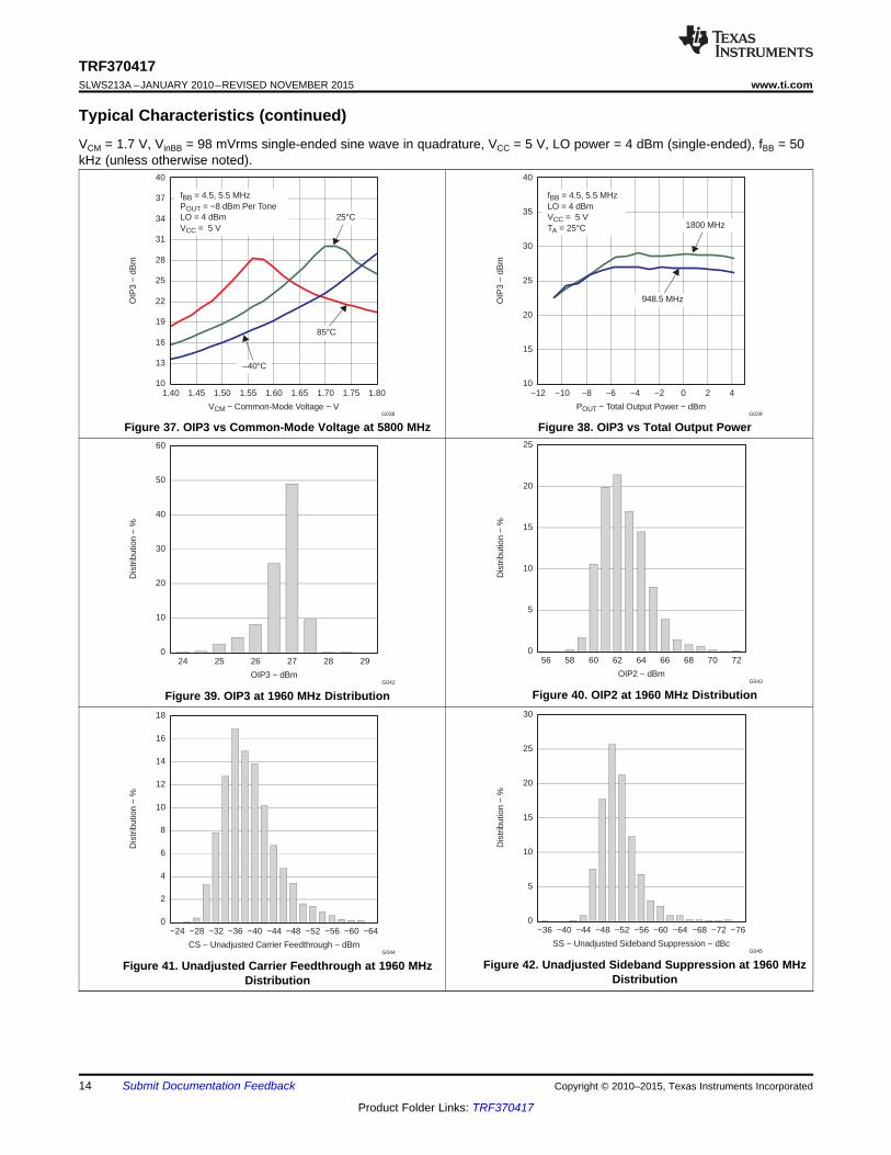
Figure 37. OIP3 vs Common-Mode Voltage at 5800 MHz Figure 38. OIP3 vs Total Output Power
Figure 40. OIP2 at 1960 MHz DistributionFigure 39. OIP3 at 1960 MHz Distribution
Figure 42. Unadjusted Sideband Suppression at 1960 MHzFigure 41. Unadjusted Carrier Feedthrough at 1960 MHzDistributionDistribution
14 Submit Documentation Feedback Copyright © 2010–2015, Texas Instruments Incorporated
Product Folder Links: TRF370417
P1dB − dBm
0
5
10
15
20
25
30
35
11.4 11.6 11.8 12 12.2 12.4
Dis
trib
utio
n −
%
G046
TRF370417www.ti.com SLWS213A –JANUARY 2010–REVISED NOVEMBER 2015
Typical Characteristics (continued)VCM = 1.7 V, VinBB = 98 mVrms single-ended sine wave in quadrature, VCC = 5 V, LO power = 4 dBm (single-ended), fBB = 50kHz (unless otherwise noted).
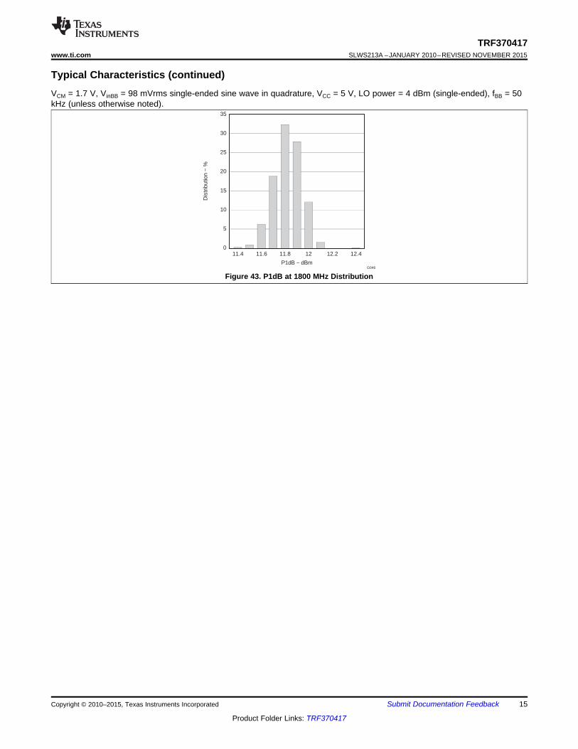
Figure 43. P1dB at 1800 MHz Distribution
Copyright © 2010–2015, Texas Instruments Incorporated Submit Documentation Feedback 15
Product Folder Links: TRF370417
VC
C2
4
GN
D2
3
BB
IN2
2
BB
IP2
1
GN
D2
0G
ND
20
GN
D1
9
VCC18
GND17
RF_OUT16
15
14 GND
13
GN
D87
BB
QN
9
BB
QP
10
GN
D11
GN
D1
2
1
2GND
3LOP
4LON
GND 5
6
0/90
S
NC
NC
B0175-01
NC
NC
NC
TRF370417SLWS213A –JANUARY 2010–REVISED NOVEMBER 2015 www.ti.com
7 Detailed Description
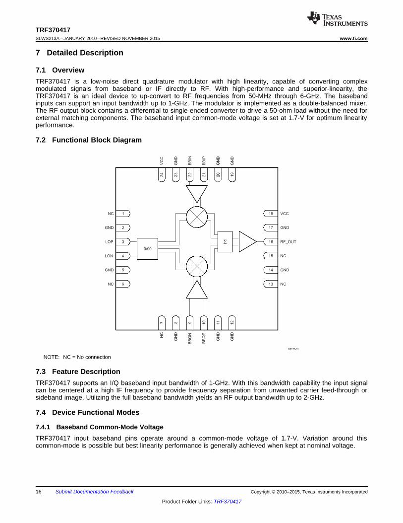
7.1 OverviewTRF370417 is a low-noise direct quadrature modulator with high linearity, capable of converting complexmodulated signals from baseband or IF directly to RF. With high-performance and superior-linearity, theTRF370417 is an ideal device to up-convert to RF frequencies from 50-MHz through 6-GHz. The basebandinputs can support an input bandwidth up to 1-GHz. The modulator is implemented as a double-balanced mixer.The RF output block contains a differential to single-ended converter to drive a 50-ohm load without the need forexternal matching components. The baseband input common-mode voltage is set at 1.7-V for optimum linearityperformance.
7.2 Functional Block Diagram
NOTE: NC = No connection
7.3 Feature DescriptionTRF370417 supports an I/Q baseband input bandwidth of 1-GHz. With this bandwidth capability the input signalcan be centered at a high IF frequency to provide frequency separation from unwanted carrier feed-through orsideband image. Utilizing the full baseband bandwidth yields an RF output bandwidth up to 2-GHz.
7.4 Device Functional Modes
7.4.1 Baseband Common-Mode VoltageTRF370417 input baseband pins operate around a common-mode voltage of 1.7-V. Variation around thiscommon-mode is possible but best linearity performance is generally achieved when kept at nominal voltage.
16 Submit Documentation Feedback Copyright © 2010–2015, Texas Instruments Incorporated
Product Folder Links: TRF370417
TRF370417www.ti.com SLWS213A –JANUARY 2010–REVISED NOVEMBER 2015
Device Functional Modes (continued)7.4.2 LO Drive LevelThe LO drive level is nominally specified at 4-dBm. The device can accept a large range of LO drive level. Ahigher drive level generally provides better output noise performance and some linearity improvement. There issome trade-off between carrier feed-through and sideband suppression performance that is dependent onfrequency and drive level. The LO drive level of 4-dB is deemed a good balance between those two parametersacross frequency.
Copyright © 2010–2015, Texas Instruments Incorporated Submit Documentation Feedback 17
Product Folder Links: TRF370417
TRF370417SLWS213A –JANUARY 2010–REVISED NOVEMBER 2015 www.ti.com
8 Application and Implementation
NOTEInformation in the following applications sections is not part of the TI componentspecification, and TI does not warrant its accuracy or completeness. TI’s customers areresponsible for determining suitability of components for their purposes. Customers shouldvalidate and test their design implementation to confirm system functionality.
8.1 Application Information
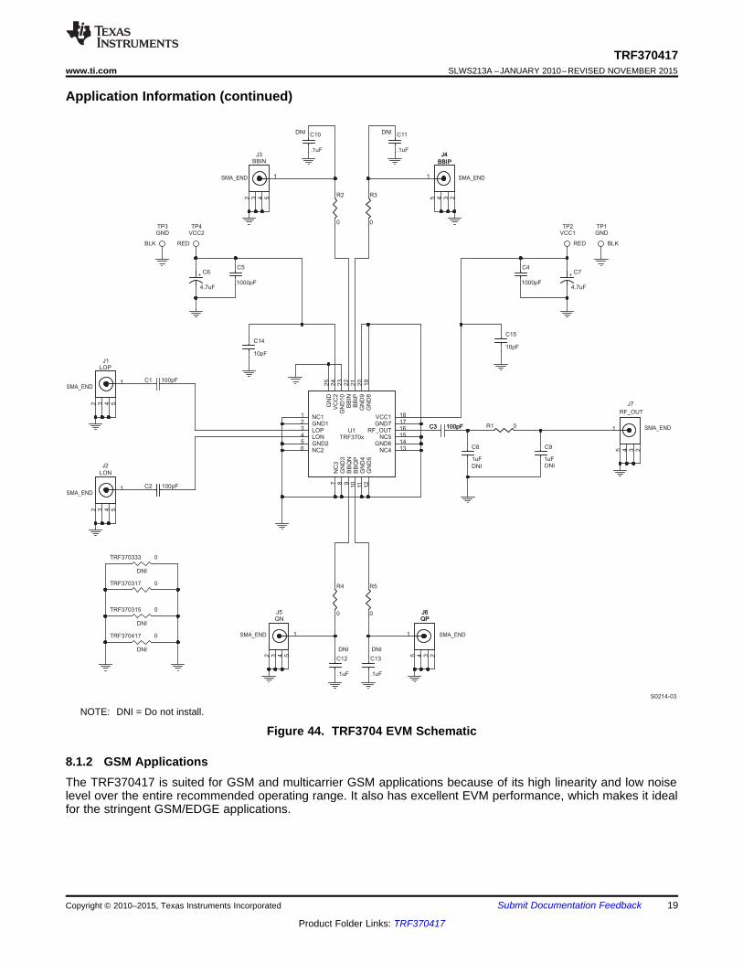
8.1.1 Basic Connections• See Figure 44 for proper connection of the TRF3704 modulator.• Connect a single power supply (4.5 V–5.5 V) to pins 18 and 24. These pins should be decoupled as shown
on pins 4, 5, 6, and 7.• Connect pins 2, 5, 8, 11, 12, 14, 17, 19, 20, and 23 to GND.• Connect a single-ended LO source of desired frequency to LOP (amplitude between –5 dBm and 12 dBm).
This should be ac-coupled through a 100-pF capacitor.• Terminate the ac-coupled LON with 50 Ω to GND.• Connect a baseband signal to pins 21 = I, 22 = I, 10 = Q, and 9 = Q.• The differential baseband inputs should be set to the proper common-mode voltage of 1.7 V.• RF_OUT, pin 16, can be fed to a spectrum analyzer set to the desired frequency, LO ± baseband signal. This
pin should also be ac-coupled through a 100-pF capacitor.• All NC pins can be left floating.
8.1.1.1 ESD SensitivityRF devices may be extremely sensitive to electrostatic discharge (ESD). To prevent damage from ESD, devicesshould be stored and handled in a way that prevents the build-up of electrostatic voltages that exceed the ratedlevel. Rated ESD levels should also not be exceeded while the device is installed on a printed circuit board(PCB). Follow these guidelines for optimal ESD protection:• Low ESD performance is not uncommon in RF ICs; see the Absolute Maximum Ratings table. Therefore,
customers’ ESD precautions should be consistent with these ratings.• The device should be robust once assembled onto the PCB unless external inputs (connectors, etc.) directly
connect the device pins to off-board circuits.
18 Submit Documentation Feedback Copyright © 2010–2015, Texas Instruments Incorporated
Product Folder Links: TRF370417
SMA_END
SMA_END SMA_END
SMA_END
SMA_ENDSMA_END
SMA_END
+C6
4.7uF
+
R4
0
C3 100pFC3 100pF
NC11
GND12
LOP3
LON4
GND25
NC26
NC
37
GN
D3
8
BB
QN
9
BB
QP
10
GN
D4
11
GN
D5
12
NC4 13GND6 14
NC5 15RF_OUT 16
GND7 17VCC1 18
GN
D8
19
GN
D9
20
BB
IP2
1B
BIN
22
GN
D1
02
3V
CC
22
4G
ND
25
R3
0
C5
1000pF
J1LOP
1
2 3 4 5
C15
10pF
C10
.1uF
DNI
R2
0
J3BBIN
1
2 3 4 5
C13
.1uF
DNI
C14
10pF
C12
.1uF
DNI
J5QN
1
2 3 4 5
J7
RF_OUT
1
2345C9
1uFDNI
C8
1uF
DNI
C1 100pF
+C7
RED BLK
4.7uF
+
J2
LON
1
2 3 4 5
J4
BBIP
J4
BBIP
1
2345
J6QPJ6QP
1
2345
C2 100pF
R1 0
0
DNI
C11
.1uF
DNI
R5
0
C4
1000pF
S0214-03
U1TRF370x
TP2VCC1
TP3GND
TP1GND
TP4VCC2
BLK RED
TRF370417
0
0
0
DNI
DNI
TRF370315
TRF370317
TRF370333
TRF370417www.ti.com SLWS213A –JANUARY 2010–REVISED NOVEMBER 2015
Application Information (continued)
NOTE: DNI = Do not install.
Figure 44. TRF3704 EVM Schematic
8.1.2 GSM ApplicationsThe TRF370417 is suited for GSM and multicarrier GSM applications because of its high linearity and low noiselevel over the entire recommended operating range. It also has excellent EVM performance, which makes it idealfor the stringent GSM/EDGE applications.
Copyright © 2010–2015, Texas Instruments Incorporated Submit Documentation Feedback 19
Product Folder Links: TRF370417
16
DAC5687
16
CLK1
RF Out
VCXO
Ref Osc
CLK2
CDCM7005
Clock Gen
TRF3761
PLL
LO Generator
TRF370x
I/Q
Modulator
B0176-02
TRF370417SLWS213A –JANUARY 2010–REVISED NOVEMBER 2015 www.ti.com
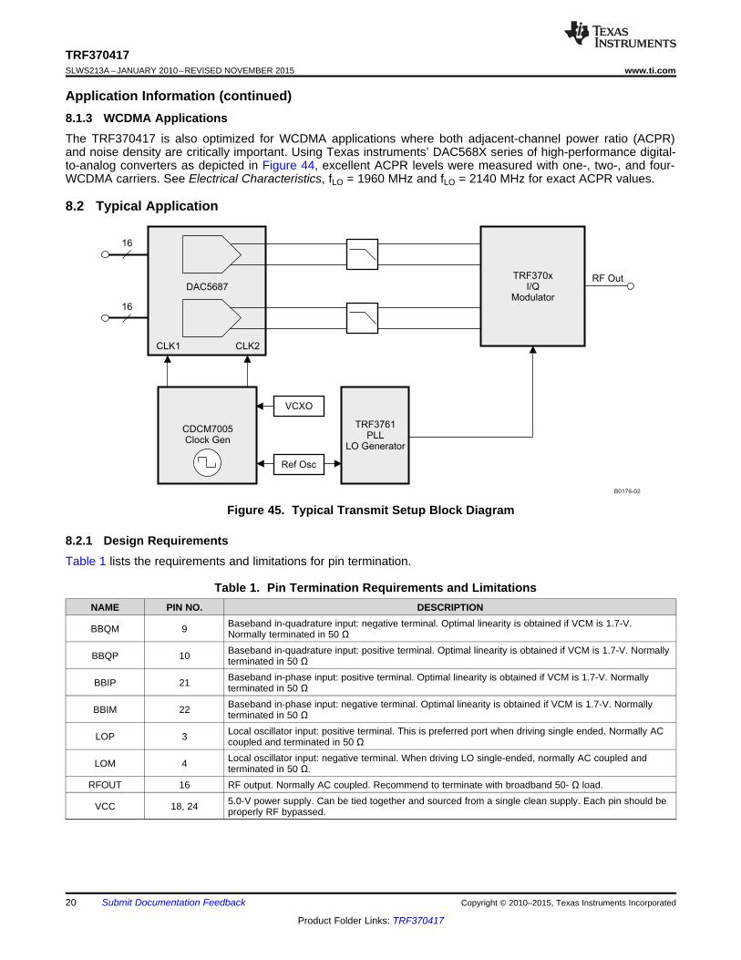
Application Information (continued)8.1.3 WCDMA ApplicationsThe TRF370417 is also optimized for WCDMA applications where both adjacent-channel power ratio (ACPR)and noise density are critically important. Using Texas instruments’ DAC568X series of high-performance digital-to-analog converters as depicted in Figure 44, excellent ACPR levels were measured with one-, two-, and four-WCDMA carriers. See Electrical Characteristics, fLO = 1960 MHz and fLO = 2140 MHz for exact ACPR values.
8.2 Typical Application
Figure 45. Typical Transmit Setup Block Diagram
8.2.1 Design RequirementsTable 1 lists the requirements and limitations for pin termination.
Table 1. Pin Termination Requirements and LimitationsNAME PIN NO. DESCRIPTION
Baseband in-quadrature input: negative terminal. Optimal linearity is obtained if VCM is 1.7-V.BBQM 9 Normally terminated in 50 ΩBaseband in-quadrature input: positive terminal. Optimal linearity is obtained if VCM is 1.7-V. NormallyBBQP 10 terminated in 50 ΩBaseband in-phase input: positive terminal. Optimal linearity is obtained if VCM is 1.7-V. NormallyBBIP 21 terminated in 50 ΩBaseband in-phase input: negative terminal. Optimal linearity is obtained if VCM is 1.7-V. NormallyBBIM 22 terminated in 50 ΩLocal oscillator input: positive terminal. This is preferred port when driving single ended. Normally ACLOP 3 coupled and terminated in 50 ΩLocal oscillator input: negative terminal. When driving LO single-ended, normally AC coupled andLOM 4 terminated in 50 Ω.
RFOUT 16 RF output. Normally AC coupled. Recommend to terminate with broadband 50- Ω load.5.0-V power supply. Can be tied together and sourced from a single clean supply. Each pin should beVCC 18, 24 properly RF bypassed.
20 Submit Documentation Feedback Copyright © 2010–2015, Texas Instruments Incorporated
Product Folder Links: TRF370417
TRF370417www.ti.com SLWS213A –JANUARY 2010–REVISED NOVEMBER 2015
8.2.2 Detailed Design Procedure
Table 2. Bill of Materials for TRF370x EVMITEM REFERENCE MFT. PARTQUANTITY VALUE PCB FOOTPRINT MFR. NAME NOTENUMBER DESIGNATOR NUMBER
1 3 C1, C2, C3 100 pF 0402 PANASONIC ECJ-0EC1H101J
2 2 C4, C5 1000 pF 0402 PANASONIC ECJ-0VC1H102J
3 2 C6, C7 4.7 μF TANT_A KERMET T491A475K016AS
ECJ-4 0 C8, C9 1 μF 0402 PANASONIC DNI0EC1H010C_DNI
C10, C11, C12, ECJ-5 0 0.1 μF 0402 PANASONIC DNIC13 0EB1A104K_DNI
GRM1555C1H100JZ06 2 C14, C15 10 pF 0402 MURATA 1D
J1, J2, J3, J4, JOHNSON7 7 LOP SMA_SMEL_250x215 142-0711-821J5, J6, J7 COMPONENTS
8 2 R1 0 0402 PANASONIC ERJ-2GE0R00 OR EQUIVALENT
9 4 R2, R3, R4, R5 0 0402 PANASONIC ERJ-2GE0R00 OR EQUIVALENT
QFN_24_163x163_ For TRF370333TRF370333 TI TRF3703330p50mm EVM, TI supplied
QFN_24_163x163_ For TRF370317TRF370317 TI TRF3703170p50mm EVM, TI supplied10 1 U1
QFN_24_163x163_ For TRF370315TRF370315 TI TRF3703150p50mm EVM, TI supplied
QFN_24_163x163_ For TRF370417TRF370417 TI TRF3704170p50mm EVM, TI supplied
11 2 TP1, TP3 BLK TP_THVT_100_RND KEYSTONE 5001K
12 2 TP2, TP4 RED TP_THVT_100_RND KEYSTONE 5000K
8.2.2.1 DAC-to-Modulator Interface NetworkFor optimum linearity and dynamic range, the digital-to-analog converter (DAC) can interface directly with themodulator; however, the common-mode voltage of each device must be maintained. A passive interface circuit isused to transform the common-mode voltage of the DAC to the desired set-point of the modulator. The passivecircuit invariably introduces some insertion loss between the two devices. In general, it is desirable to keep theinsertion loss as low as possible to achieve the best dynamic range. Figure 46 shows the passive interconnectcircuit for two different topologies. One topology is used when the DAC (such as the DAC568x) common-mode islarger than the modulator. The voltage Vee is nominally set to ground, but can be set to a negative voltage toreduce the insertion loss of the network. The second topology is used when the DAC (such as the DAC56x2)common-mode is smaller than the modulator. Note that this passive interconnect circuit is duplicated for each ofthe differential I/Q branches.
Copyright © 2010–2015, Texas Instruments Incorporated Submit Documentation Feedback 21
Product Folder Links: TRF370417
R1
R2
R3Id
DAC568x TRF370x
It
Vdd
3.3V
1.7V
Vee
Vdd
R1
R2
R3Id
It
DAC56x2 TRF370x
1.7V
0.7V
Topology 1: DAC Vcm > TRF370x Vcm
Topology 2: DAC Vcm < TRF370x Vcm
S0338-01
TRF370417SLWS213A –JANUARY 2010–REVISED NOVEMBER 2015 www.ti.com
Figure 46. Passive DAC-to-Modulator Interface Network
Table 3. DAC-to-Modulator Interface Network ValuesTOPOLOGY 1
TOPOLOGY 2WITH VEE = 0 V WITH VEE = 5 V
DAC Vcm [V] 3.3 3.3 0.7TRF370x Vcm [V] 1.7 1.7 1.7Vdd [V] 5 5 5Vee [V] Gnd –5 N/AR1 [Ω] 66 56 960R2 [Ω] 100 80 290R3 [Ω] 108 336 52Insertion loss [dB] 5.8 1.9 2.3
22 Submit Documentation Feedback Copyright © 2010–2015, Texas Instruments Incorporated
Product Folder Links: TRF370417
POUT − Output Power − dBm
−90
−87
−84
−81
−78
−75
−72
−69
−66
−63
−60
−20 −18 −16 −14 −12 −10 −8 −6 −4
AC
PR
−A
dja
cent
Channel P
ow
er
Ratio
−dB
c
G040
One Carrier, WCDMA at 1960 MHz
DAC5687 as Source with 2.5 MHz LPF
Adj
Alt
POUT − Output Power − dBm
−90
−87
−84
−81
−78
−75
−72
−69
−66
−63
−60
−20 −18 −16 −14 −12 −10 −8 −6 −4
AC
PR
−A
dja
cent
Channel P
ow
er
Ratio
−dB
c
G041
One Carrier, WCDMA at 2140 MHz
DAC5687 as Source with 2.5 MHz LPF
Adj
Alt
TRF370417www.ti.com SLWS213A –JANUARY 2010–REVISED NOVEMBER 2015
8.2.3 Application Curves
Figure 47. Adjacent Channel Power Ratio vs Output Power Figure 48. Adjacent Channel Power Ratio vs. Outputat 1960 MHz Power at 2140 MHz
9 Power Supply RecommendationsThe TRF370417 is powered by supplying a nominal 5 V to pins 18 and 24. These supplies can be tied togetherand sourced from a single clean supply. Proper RF bypassing should be placed close to each power supply pin.Ground pin connections should have at least one ground via close to each ground pin to minimize groundinductance. The thermal pad must be tied to ground, preferably with the recommended ground via pattern toprovide a good thermal conduction path to the alternate side of the board and to provide a good RF ground forthe device. (Refer to Layout Guidelines for additional information.)
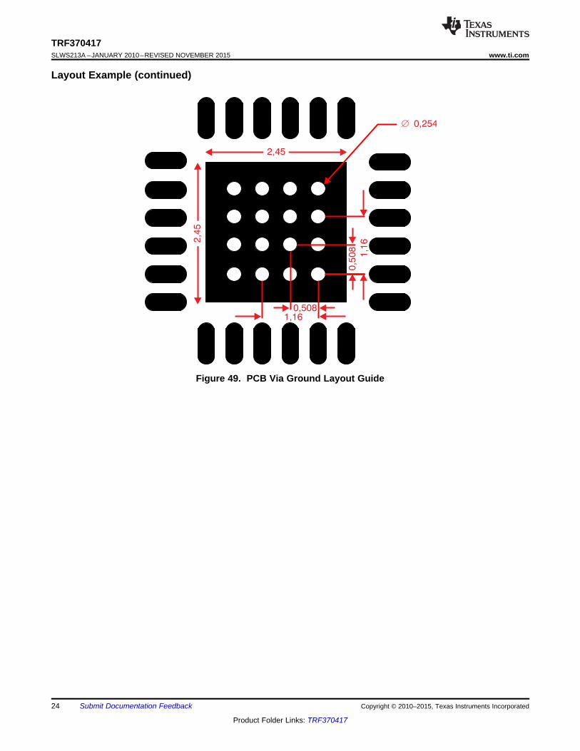
10 Layout
10.1 Layout GuidelinesThe TRF370417 device is fitted with a ground slug on the back of the package that must be soldered to theprinted circuit board (PCB) ground with adequate ground vias to ensure a good thermal and electricalconnection. The recommended via pattern and ground pad dimensions are shown in Figure 76. Therecommended via diameter is 10 mils (0.10 in or 0.25 mm). The ground pins of the device can be directly tied tothe ground slug pad for a low-inductance path to ground. Additional ground vias may be added if space allows.Decoupling capacitors at each of the supply pins are strongly recommended. The value of these capacitorsshould be chosen to provide a low-impedance RF path to ground at the frequency of operation. Typically, thevalue of these capacitors is approximately 10 pF or lower. The device exhibits symmetry with respect to thequadrature input paths. TI recommends that the PCB layout maintain this symmetry to ensure that thequadrature balance of the device is not impaired. The I/Q input traces should be routed as differential pairs andthe respective lengths all kept equal to each other. On the RF traces, maintain proper trace widths to keep thecharacteristic impedance of the RF traces at a nominal 50 Ω.
10.2 Layout ExampleFigure 49 shows the top view of the TRF3704 EVM board.
Copyright © 2010–2015, Texas Instruments Incorporated Submit Documentation Feedback 23
Product Folder Links: TRF370417
2,4
5
1,1
6
2,45
Æ 0,254
1,160,508
0,5
08
TRF370417SLWS213A –JANUARY 2010–REVISED NOVEMBER 2015 www.ti.com
Layout Example (continued)
Figure 49. PCB Via Ground Layout Guide
24 Submit Documentation Feedback Copyright © 2010–2015, Texas Instruments Incorporated
Product Folder Links: TRF370417
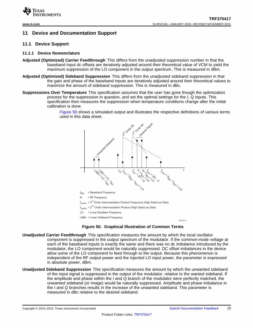
f
f
fn
f
f
LO
LSBn
BBn
3rdH/L
2ndH/L
BBn
BBn
BBn
BBn
BBn
BBn
rd
rd
rd
rd
rd
rd
3
2
rd
nd
= Baseband Frequency
= RF Frequency
= 3 Order Intermodulation Product Frequency (High Side/Low Side)
= 2 Order
rd
ndIntermodulation Product (High Side/Low Side)
= Local Oscillator Frequency
= Lower Sideband Frequency
BBn
rd
BBn
BBn
BBn
BBn
BBn
rd
rd
rd
rd
rd
Unw
ante
d Sideb
and
2
Ord
er IM
nd 3Ord
er IM
rd
Des
ired
Signa
l
LSB2 = LO
–fBB2
LSB1 = LO
–fBB1
LO f
= (f
–f
) + LO
2ndL
BB2
BB1
f
= 2f1–
f2
3rdL
f1 = f
+ LO
BB1
f2 = f
+ LO
BB2
f
= 2f2–
f1
3rdH
f
= (f
+ f
) + LO
2ndH
BB2
BB1
M0104-01
TRF370417www.ti.com SLWS213A –JANUARY 2010–REVISED NOVEMBER 2015
11 Device and Documentation Support
11.1 Device Support
11.1.1 Device NomenclatureAdjusted (Optimized) Carrier Feedthrough This differs from the unadjusted suppression number in that the
baseband input dc offsets are iteratively adjusted around their theoretical value of VCM to yield themaximum suppression of the LO component in the output spectrum. This is measured in dBm.
Adjusted (Optimized) Sideband Suppression This differs from the unadjusted sideband suppression in thatthe gain and phase of the baseband inputs are iteratively adjusted around their theoretical values tomaximize the amount of sideband suppression. This is measured in dBc.
Suppressions Over Temperature This specification assumes that the user has gone though the optimizationprocess for the suppression in question, and set the optimal settings for the I, Q inputs. Thisspecification then measures the suppression when temperature conditions change after the initialcalibration is done.
Figure 50 shows a simulated output and illustrates the respective definitions of various termsused in this data sheet.
Figure 50. Graphical Illustration of Common Terms
Unadjusted Carrier Feedthrough This specification measures the amount by which the local oscillatorcomponent is suppressed in the output spectrum of the modulator. If the common-mode voltage ateach of the baseband inputs is exactly the same and there was no dc imbalance introduced by themodulator, the LO component would be naturally suppressed. DC offset imbalances in the deviceallow some of the LO component to feed through to the output. Because this phenomenon isindependent of the RF output power and the injected LO input power, the parameter is expressedin absolute power, dBm.
Unadjusted Sideband Suppression This specification measures the amount by which the unwanted sidebandof the input signal is suppressed in the output of the modulator, relative to the wanted sideband. Ifthe amplitude and phase within the I and Q branch of the modulator were perfectly matched, theunwanted sideband (or image) would be naturally suppressed. Amplitude and phase imbalance inthe I and Q branches results in the increase of the unwanted sideband. This parameter ismeasured in dBc relative to the desired sideband.
Copyright © 2010–2015, Texas Instruments Incorporated Submit Documentation Feedback 25
Product Folder Links: TRF370417
TRF370417SLWS213A –JANUARY 2010–REVISED NOVEMBER 2015 www.ti.com
11.2 Documentation Support
11.2.1 Related DocumentationFor related documentation, see the documents that follow:• TRF370x User's Guide• TRF370417: Optimizing OIP3 Performance at Local Oscillator (LO) Frequencies Beyond 4.5 GHz• High Bandwidth, High Frequency Transmitter Reference Design
11.3 Community ResourcesThe following links connect to TI community resources. Linked contents are provided "AS IS" by the respectivecontributors. They do not constitute TI specifications and do not necessarily reflect TI's views; see TI's Terms ofUse.
TI E2E™ Online Community TI's Engineer-to-Engineer (E2E) Community. Created to foster collaborationamong engineers. At e2e.ti.com, you can ask questions, share knowledge, explore ideas and helpsolve problems with fellow engineers.
Design Support TI's Design Support Quickly find helpful E2E forums along with design support tools andcontact information for technical support.
11.4 TrademarksE2E is a trademark of Texas Instruments.All other trademarks are the property of their respective owners.
11.5 Electrostatic Discharge CautionThese devices have limited built-in ESD protection. The leads should be shorted together or the device placed in conductive foamduring storage or handling to prevent electrostatic damage to the MOS gates.
11.6 GlossarySLYZ022 — TI Glossary.
This glossary lists and explains terms, acronyms, and definitions.
12 Mechanical, Packaging, and Orderable InformationThe following pages include mechanical, packaging, and orderable information. This information is the mostcurrent data available for the designated devices. This data is subject to change without notice and revision ofthis document. For browser-based versions of this data sheet, refer to the left-hand navigation.
26 Submit Documentation Feedback Copyright © 2010–2015, Texas Instruments Incorporated
Product Folder Links: TRF370417
PACKAGE OPTION ADDENDUM
www.ti.com 3-Nov-2015
Addendum-Page 1
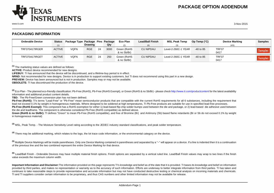
PACKAGING INFORMATION
Orderable Device Status(1)
Package Type PackageDrawing
Pins PackageQty
Eco Plan(2)
Lead/Ball Finish(6)
MSL Peak Temp(3)
Op Temp (°C) Device Marking(4/5)
Samples
TRF370417IRGER ACTIVE VQFN RGE 24 3000 Green (RoHS& no Sb/Br)
CU NIPDAU Level-2-260C-1 YEAR -40 to 85 TRF370417
TRF370417IRGET ACTIVE VQFN RGE 24 250 Green (RoHS& no Sb/Br)
CU NIPDAU Level-2-260C-1 YEAR -40 to 85 TRF370417
(1) The marketing status values are defined as follows:ACTIVE: Product device recommended for new designs.LIFEBUY: TI has announced that the device will be discontinued, and a lifetime-buy period is in effect.NRND: Not recommended for new designs. Device is in production to support existing customers, but TI does not recommend using this part in a new design.PREVIEW: Device has been announced but is not in production. Samples may or may not be available.OBSOLETE: TI has discontinued the production of the device.
(2) Eco Plan - The planned eco-friendly classification: Pb-Free (RoHS), Pb-Free (RoHS Exempt), or Green (RoHS & no Sb/Br) - please check http://www.ti.com/productcontent for the latest availabilityinformation and additional product content details.TBD: The Pb-Free/Green conversion plan has not been defined.Pb-Free (RoHS): TI's terms "Lead-Free" or "Pb-Free" mean semiconductor products that are compatible with the current RoHS requirements for all 6 substances, including the requirement thatlead not exceed 0.1% by weight in homogeneous materials. Where designed to be soldered at high temperatures, TI Pb-Free products are suitable for use in specified lead-free processes.Pb-Free (RoHS Exempt): This component has a RoHS exemption for either 1) lead-based flip-chip solder bumps used between the die and package, or 2) lead-based die adhesive used betweenthe die and leadframe. The component is otherwise considered Pb-Free (RoHS compatible) as defined above.Green (RoHS & no Sb/Br): TI defines "Green" to mean Pb-Free (RoHS compatible), and free of Bromine (Br) and Antimony (Sb) based flame retardants (Br or Sb do not exceed 0.1% by weightin homogeneous material)
(3) MSL, Peak Temp. - The Moisture Sensitivity Level rating according to the JEDEC industry standard classifications, and peak solder temperature.
(4) There may be additional marking, which relates to the logo, the lot trace code information, or the environmental category on the device.
(5) Multiple Device Markings will be inside parentheses. Only one Device Marking contained in parentheses and separated by a "~" will appear on a device. If a line is indented then it is a continuationof the previous line and the two combined represent the entire Device Marking for that device.
(6) Lead/Ball Finish - Orderable Devices may have multiple material finish options. Finish options are separated by a vertical ruled line. Lead/Ball Finish values may wrap to two lines if the finishvalue exceeds the maximum column width.
Important Information and Disclaimer:The information provided on this page represents TI's knowledge and belief as of the date that it is provided. TI bases its knowledge and belief on informationprovided by third parties, and makes no representation or warranty as to the accuracy of such information. Efforts are underway to better integrate information from third parties. TI has taken andcontinues to take reasonable steps to provide representative and accurate information but may not have conducted destructive testing or chemical analysis on incoming materials and chemicals.TI and TI suppliers consider certain information to be proprietary, and thus CAS numbers and other limited information may not be available for release.
PACKAGE OPTION ADDENDUM
www.ti.com 3-Nov-2015
Addendum-Page 2
In no event shall TI's liability arising out of such information exceed the total purchase price of the TI part(s) at issue in this document sold by TI to Customer on an annual basis.
TAPE AND REEL INFORMATION
*All dimensions are nominal
Device PackageType
PackageDrawing
Pins SPQ ReelDiameter
(mm)
ReelWidth
W1 (mm)
A0(mm)
B0(mm)
K0(mm)
P1(mm)
W(mm)
Pin1Quadrant
TRF370417IRGER VQFN RGE 24 3000 330.0 12.4 4.3 4.3 1.5 8.0 12.0 Q1
TRF370417IRGET VQFN RGE 24 250 180.0 12.4 4.3 4.3 1.5 8.0 12.0 Q1
PACKAGE MATERIALS INFORMATION
www.ti.com 2-Nov-2016
Pack Materials-Page 1
*All dimensions are nominal
Device Package Type Package Drawing Pins SPQ Length (mm) Width (mm) Height (mm)
TRF370417IRGER VQFN RGE 24 3000 336.6 336.6 28.6
TRF370417IRGET VQFN RGE 24 250 210.0 185.0 35.0
PACKAGE MATERIALS INFORMATION
www.ti.com 2-Nov-2016
Pack Materials-Page 2
GENERIC PACKAGE VIEW
Images above are just a representation of the package family, actual package may vary.Refer to the product data sheet for package details.
RGE 24 VQFN - 1 mm max heightPLASTIC QUAD FLATPACK - NO LEAD
4204104/H
www.ti.com
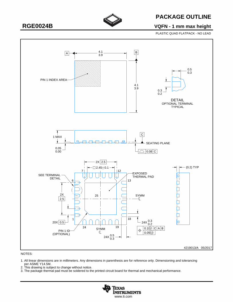
PACKAGE OUTLINE
C
SEE TERMINALDETAIL
24X 0.30.2
2.45 0.1
24X 0.50.3
1 MAX
(0.2) TYP
0.050.00
20X 0.5
2X2.5
2X 2.5
A 4.13.9
B
4.13.9
0.30.2
0.50.3
VQFN - 1 mm max heightRGE0024BPLASTIC QUAD FLATPACK - NO LEAD
4219013/A 05/2017
PIN 1 INDEX AREA
0.08 C
SEATING PLANE
1
6 13
18
7 12
24 19
(OPTIONAL)PIN 1 ID
0.1 C A B0.05
EXPOSEDTHERMAL PAD
25 SYMM
SYMM
NOTES: 1. All linear dimensions are in millimeters. Any dimensions in parenthesis are for reference only. Dimensioning and tolerancing per ASME Y14.5M. 2. This drawing is subject to change without notice. 3. The package thermal pad must be soldered to the printed circuit board for thermal and mechanical performance.
SCALE 3.000
DETAILOPTIONAL TERMINAL
TYPICAL
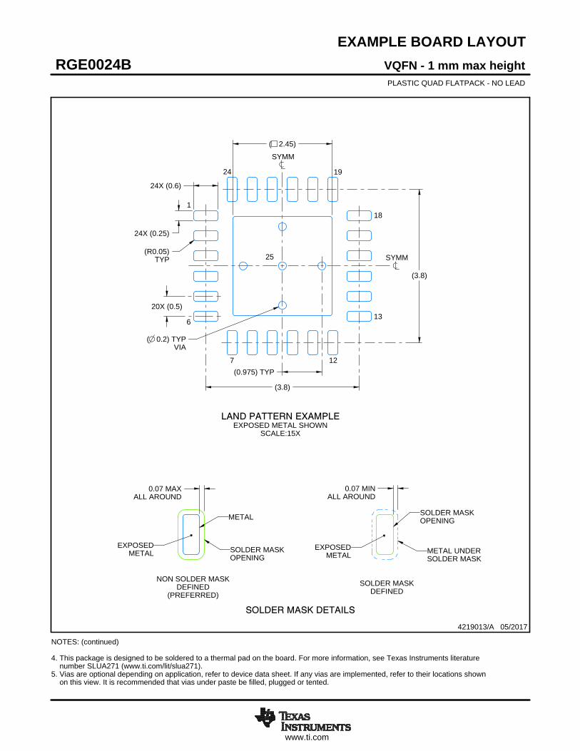
www.ti.com
EXAMPLE BOARD LAYOUT
0.07 MINALL AROUND
0.07 MAXALL AROUND
24X (0.25)
24X (0.6)
( 0.2) TYPVIA
20X (0.5)
(3.8)
(3.8)
( 2.45)
(R0.05)TYP
(0.975) TYP
VQFN - 1 mm max heightRGE0024BPLASTIC QUAD FLATPACK - NO LEAD
4219013/A 05/2017
SYMM
1
6
7 12
13
18
1924
SYMM
LAND PATTERN EXAMPLEEXPOSED METAL SHOWN
SCALE:15X
NOTES: (continued) 4. This package is designed to be soldered to a thermal pad on the board. For more information, see Texas Instruments literature number SLUA271 (www.ti.com/lit/slua271).5. Vias are optional depending on application, refer to device data sheet. If any vias are implemented, refer to their locations shown on this view. It is recommended that vias under paste be filled, plugged or tented.
25
SOLDER MASKOPENING
METAL UNDERSOLDER MASK
SOLDER MASKDEFINED
EXPOSEDMETAL
METAL
SOLDER MASKOPENING
SOLDER MASK DETAILS
NON SOLDER MASKDEFINED
(PREFERRED)
EXPOSEDMETAL
www.ti.com
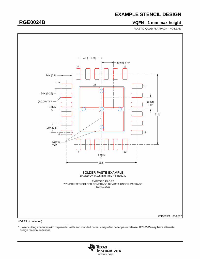
EXAMPLE STENCIL DESIGN
24X (0.6)
24X (0.25)
20X (0.5)
(3.8)
(3.8)
4X ( 1.08)
(0.64)TYP
(0.64) TYP
(R0.05) TYP
VQFN - 1 mm max heightRGE0024BPLASTIC QUAD FLATPACK - NO LEAD
4219013/A 05/2017
NOTES: (continued) 6. Laser cutting apertures with trapezoidal walls and rounded corners may offer better paste release. IPC-7525 may have alternate design recommendations.
25
SYMM
METALTYP
SOLDER PASTE EXAMPLEBASED ON 0.125 mm THICK STENCIL
EXPOSED PAD 25
78% PRINTED SOLDER COVERAGE BY AREA UNDER PACKAGESCALE:20X
SYMM
1
6
7 12
13
18
1924
IMPORTANT NOTICE
Texas Instruments Incorporated (TI) reserves the right to make corrections, enhancements, improvements and other changes to itssemiconductor products and services per JESD46, latest issue, and to discontinue any product or service per JESD48, latest issue. Buyersshould obtain the latest relevant information before placing orders and should verify that such information is current and complete.TI’s published terms of sale for semiconductor products (http://www.ti.com/sc/docs/stdterms.htm) apply to the sale of packaged integratedcircuit products that TI has qualified and released to market. Additional terms may apply to the use or sale of other types of TI products andservices.Reproduction of significant portions of TI information in TI data sheets is permissible only if reproduction is without alteration and isaccompanied by all associated warranties, conditions, limitations, and notices. TI is not responsible or liable for such reproduceddocumentation. Information of third parties may be subject to additional restrictions. Resale of TI products or services with statementsdifferent from or beyond the parameters stated by TI for that product or service voids all express and any implied warranties for theassociated TI product or service and is an unfair and deceptive business practice. TI is not responsible or liable for any such statements.Buyers and others who are developing systems that incorporate TI products (collectively, “Designers”) understand and agree that Designersremain responsible for using their independent analysis, evaluation and judgment in designing their applications and that Designers havefull and exclusive responsibility to assure the safety of Designers' applications and compliance of their applications (and of all TI productsused in or for Designers’ applications) with all applicable regulations, laws and other applicable requirements. Designer represents that, withrespect to their applications, Designer has all the necessary expertise to create and implement safeguards that (1) anticipate dangerousconsequences of failures, (2) monitor failures and their consequences, and (3) lessen the likelihood of failures that might cause harm andtake appropriate actions. Designer agrees that prior to using or distributing any applications that include TI products, Designer willthoroughly test such applications and the functionality of such TI products as used in such applications.TI’s provision of technical, application or other design advice, quality characterization, reliability data or other services or information,including, but not limited to, reference designs and materials relating to evaluation modules, (collectively, “TI Resources”) are intended toassist designers who are developing applications that incorporate TI products; by downloading, accessing or using TI Resources in anyway, Designer (individually or, if Designer is acting on behalf of a company, Designer’s company) agrees to use any particular TI Resourcesolely for this purpose and subject to the terms of this Notice.TI’s provision of TI Resources does not expand or otherwise alter TI’s applicable published warranties or warranty disclaimers for TIproducts, and no additional obligations or liabilities arise from TI providing such TI Resources. TI reserves the right to make corrections,enhancements, improvements and other changes to its TI Resources. TI has not conducted any testing other than that specificallydescribed in the published documentation for a particular TI Resource.Designer is authorized to use, copy and modify any individual TI Resource only in connection with the development of applications thatinclude the TI product(s) identified in such TI Resource. NO OTHER LICENSE, EXPRESS OR IMPLIED, BY ESTOPPEL OR OTHERWISETO ANY OTHER TI INTELLECTUAL PROPERTY RIGHT, AND NO LICENSE TO ANY TECHNOLOGY OR INTELLECTUAL PROPERTYRIGHT OF TI OR ANY THIRD PARTY IS GRANTED HEREIN, including but not limited to any patent right, copyright, mask work right, orother intellectual property right relating to any combination, machine, or process in which TI products or services are used. Informationregarding or referencing third-party products or services does not constitute a license to use such products or services, or a warranty orendorsement thereof. Use of TI Resources may require a license from a third party under the patents or other intellectual property of thethird party, or a license from TI under the patents or other intellectual property of TI.TI RESOURCES ARE PROVIDED “AS IS” AND WITH ALL FAULTS. TI DISCLAIMS ALL OTHER WARRANTIES ORREPRESENTATIONS, EXPRESS OR IMPLIED, REGARDING RESOURCES OR USE THEREOF, INCLUDING BUT NOT LIMITED TOACCURACY OR COMPLETENESS, TITLE, ANY EPIDEMIC FAILURE WARRANTY AND ANY IMPLIED WARRANTIES OFMERCHANTABILITY, FITNESS FOR A PARTICULAR PURPOSE, AND NON-INFRINGEMENT OF ANY THIRD PARTY INTELLECTUALPROPERTY RIGHTS. TI SHALL NOT BE LIABLE FOR AND SHALL NOT DEFEND OR INDEMNIFY DESIGNER AGAINST ANY CLAIM,INCLUDING BUT NOT LIMITED TO ANY INFRINGEMENT CLAIM THAT RELATES TO OR IS BASED ON ANY COMBINATION OFPRODUCTS EVEN IF DESCRIBED IN TI RESOURCES OR OTHERWISE. IN NO EVENT SHALL TI BE LIABLE FOR ANY ACTUAL,DIRECT, SPECIAL, COLLATERAL, INDIRECT, PUNITIVE, INCIDENTAL, CONSEQUENTIAL OR EXEMPLARY DAMAGES INCONNECTION WITH OR ARISING OUT OF TI RESOURCES OR USE THEREOF, AND REGARDLESS OF WHETHER TI HAS BEENADVISED OF THE POSSIBILITY OF SUCH DAMAGES.Unless TI has explicitly designated an individual product as meeting the requirements of a particular industry standard (e.g., ISO/TS 16949and ISO 26262), TI is not responsible for any failure to meet such industry standard requirements.Where TI specifically promotes products as facilitating functional safety or as compliant with industry functional safety standards, suchproducts are intended to help enable customers to design and create their own applications that meet applicable functional safety standardsand requirements. Using products in an application does not by itself establish any safety features in the application. Designers mustensure compliance with safety-related requirements and standards applicable to their applications. Designer may not use any TI products inlife-critical medical equipment unless authorized officers of the parties have executed a special contract specifically governing such use.Life-critical medical equipment is medical equipment where failure of such equipment would cause serious bodily injury or death (e.g., lifesupport, pacemakers, defibrillators, heart pumps, neurostimulators, and implantables). Such equipment includes, without limitation, allmedical devices identified by the U.S. Food and Drug Administration as Class III devices and equivalent classifications outside the U.S.TI may expressly designate certain products as completing a particular qualification (e.g., Q100, Military Grade, or Enhanced Product).Designers agree that it has the necessary expertise to select the product with the appropriate qualification designation for their applicationsand that proper product selection is at Designers’ own risk. Designers are solely responsible for compliance with all legal and regulatoryrequirements in connection with such selection.Designer will fully indemnify TI and its representatives against any damages, costs, losses, and/or liabilities arising out of Designer’s non-compliance with the terms and provisions of this Notice.
Mailing Address: Texas Instruments, Post Office Box 655303, Dallas, Texas 75265Copyright © 2018, Texas Instruments Incorporated