Embed Size (px)
Citation preview

1. Introduction
As the United States’ national measurement institute,the National Institute of Standards and Technology(NIST) assists all stakeholders in selected fields withtheir measurement and standards needs. The goal ofNIST’s involvement is to enhance efficiency and pro-ductivity and increase the rate of technological innova-tion. NIST is not a regulatory agency, but rather servesas a neutral third party, often providing technical inputin matters related to measurements and standards to avariety of customers: industry, universities, nationaland international standards committees, where appro-priate. NIST recently accepted the challenge to seewhether the United States Measurement System(USMS) is meeting the nation’s measurement needs,and thus produced an assessment of the USMS inJanuary 2007 [1]. The semiconductor industry was oneof the areas considered in terms of its measurement
needs for accelerating technological innovation. Theset of measurement needs required to meet the techni-cal challenges cited in the Metrology Chapter of the2005 International Technology Roadmap forSemiconductors [2] was used to examine the status ofmeasurements and standards for accelerated technolog-ical innovation in the semiconductor industry. Thispaper presents an analysis based on selected case stud-ies of those measurement needs that the semiconductorindustry submitted to NIST.
The successes of the semiconductor industry led tomajor impacts on many other industries, such as thosethat support computers, networks, information tech-nologies, entertainment, healthcare, and defense.Advances powered by semiconductors gave businessesand consumers new flexibility, freedom, and opportuni-ty. Activities that once confined people to the home oroffice can now be performed at any time, any place, andalmost anywhere in the world. The semiconductor
Volume 112, Number 1, January-February 2007Journal of Research of the National Institute of Standards and Technology
25
[J. Res. Natl. Inst. Stand. Technol. 112, 25-38 (2007)]
Will Future Measurement Needs of theSemiconductor Industry Be Met?
Volume 112 Number 1 January-February 2007
Herbert S. Bennett
National Institute of Standardsand Technology,Gaithersburg, MD 20899
We discuss the ability of the nation’smeasurement system to meet futuremetrology needs of the semiconductorindustry. Lacking an acceptable metric forassessing the health of metrology for thesemiconductor industry, we identify alimited set of unmet measurement needs.Assuming that this set of needs may serveas proxy for the galaxy of semiconductormeasurement needs, we examine it fromthe perspective of what will be required tocontinue the semiconductor industry’spowerful impact in the world’s macro-economy and maintain its exceptionalrecord of numerous technological innova-tions. This paper concludes with sugges-
tions about ways to strengthen the meas-urement system for the semiconductorindustry.
Key words: economic forces; measure-ment needs; metrology; semiconductorindustry; standards; technological innova-tion; technology roadmaps; United StatesMeasurement System (USMS).
Accepted: December 22, 2006
Available online: http://www.nist.gov/jres

industry is bringing new opportunities, socio-economicadvances, and progress to nations and societies aroundthe world. The semiconductor industry contributes sub-stantially to overall global economic health and isentering an era of global private-public-governmentpartnerships to meet future challenges.
The scope of the analysis given here is primarilyfrom the perspective of the 2005 Edition of theInternational Technology Roadmap for Semiconductors(ITRS) [2], which includes semiconductor memories,microprocessors, signal processors, radio frequencyand analog/mixed signal circuits, logic devices, andemerging research devices and materials. It does notinclude semiconductors for power electronics used intransportation systems and for optoelectronic compo-nents used in telecommunications systems.
In this paper, we are analyzing the USMS as a sys-tem that supports the semiconductor industry. Using alimited data base, we have taken a “snapshot”, not a“video”, of the semiconductor part of the USMS. Weare not assessing measurement needs in detail; nor anyarea in depth. Neither are we assigning any prioritiesfor addressing the measurement needs and barriers totechnological innovation in the semiconductor industry.Considering these caveats; we certainly do not suggestthat readers limit their horizons to the focus of thisanalysis on specific topics cited in Appendix 1. Also,the illustrative topics given here may not lead in thefuture to optimal solutions and, therefore, may not bethe actual solutions adopted by the semiconductorindustry. For example, optical scatterometry is not citedin Appendix 1, but it has great potential for the difficultchallenge cited in Table 1 of nondestructive, productionworthy wafer inspection for critical dimensions.
2. Semiconductor Industry Structure
The semiconductor industry consists of companies,trade associations, research and development consortia,universities, and governments that contribute to theeconomic well-being of many nations. Its main prod-ucts and players are listed in the following two sub-sec-tions.
2.1 Semiconductor Products
The International Electronics ManufacturingInitiative (iNEMI), http://www.inemi.org, and theSemiconductor Industry Association (SIA),http://www.sia-online.org, have essentially orthogonalways to classify semiconductor products. The iNEMI
considers broad applications and their technical attrib-utes, which it calls product emulators. The SIA consid-ers semiconductor components, each of which hasmany applications in the iNEMI classification scheme.
The 2004 iNEMI Roadmap [3] uses the followingseven product applications and technology attributes asthe framework in which to present its findings:
Portable / Consumer - High volume consumer prod-ucts for which cost is the primary driver.
System in a Package - Complete function provided ina package to system manufacturers.
Office Systems / Large Business Systems - Productswhich seek maximum performance from a fewthousand dollar cost limit to almost no cost limit.
Network / Datacom / Telecom Products - Productsthat serve the networking, datacom and telecommarkets and cover a wide range of cost and per-formance targets.
Medical Products - Products which must operatewithin a high reliability environment.
Automotive - Products which must operate in anautomotive environment.
Defense and Aerospace - Products which must oper-ate in extreme environments.
The SIA [4] presents market data and trends forthe following products: Discrete Components,Optoelectronics, Analog, Metal Oxide Semiconductor(MOS), Logic, Microprocessor, Microcontrollers,Digital Signal Processors, Dynamic Random AccessMemory (DRAM), and Flash Memory.
2.2 Major Players
The major players are: Device Manufacturers,Equipment Manufacturers, Materials Manufacturers,Sub-Systems and Components Parts Suppliers, FactoryControl and Facilities Management, Providers ofSoftware for Design and Manufacturing,Manufacturing Services Providers, Business Servicesand Consulting Providers, Vendors for SupportProducts and Consumable Materials, TradeAssociations, Research and Development Consortia,Universities, Governments, World Trade Organization,Regulatory Agencies, and Legislators.
The ITRS has more than 1200 international contrib-utors. Their affiliations are chip makers 58 %; equip-ment and materials suppliers 21 %; consortia, researchinstitutes, and universities 18 %, and others 3 %. Theirgeographic locations are USA 52 %, Japan 18 %,Taiwan 16 %, Europe 9 %, and Korea 5 %. The web-
Volume 112, Number 1, January-February 2007Journal of Research of the National Institute of Standards and Technology
26

sites: http://www.inemi.org/cms/about/members.html,h t t p : / / w w w. s i a - o n l i n e . o r g / m e m _ l i s t . c f m ,http://wps2a.semi.org/wps/portal/_pagr/119/_pa.119/214, and http://www.sematech.org/, contain lists ofmembers, respectively, for iNEMI, SIA, SEMI, andSEMATECH/International SEMATECH.
Several semiconductor trade associations formed theWorld Semiconductor Council (WSC, http://www.semiconductorcouncil.org) in 1999. The WSC consists ofthe following trade associations from around the world:European Semiconductor Industry Association (EECA-ESIA, http://www.eeca.org), Japan Electronics andInformation Technology Industries AssociationSemiconductor Board - Japanese SemiconductorIndustry Association (JEITA-JSIA, http://semicon.jeita.or.jp/en/), Korea Semiconductor Industry Association(KSIA, http://www.ksia.or.kr), U.S. SemiconductorIndustry Association (SIA, http://www.sia-online.org),and Taiwan Semiconductor Industry Association(TSIA, http://www.tsia.org.tw). The purpose of the WSCis to promote cooperative semiconductor industryactivities, and expand international cooperation in thesemiconductor sector in order to facilitate the healthygrowth of the industry from a long-term, global per-spective.
Other major players include research consortia.These are often industry-university-government part-nerships. Examples include the SemiconductorResearch Corporation (SRC), http://www.src.org/member/about/membercompanies.asp; MicroelectronicsAdvanced Research Corporation (MARCO) /FocusCenter Research Program (FCRP), http://fcrp.src.org/Default.asp?bhcp=1; Advanced Materials ResearchCenter, http://www.amrctx.org/; InteruniversityMicroelectronics Center (IMEC), http://www.imec.be;and Semiconductor Leading Edge Technologies, Inc.(SELETE), http://www.selete.co.jp/index_e.html.
3. Economic Dimensions of Industry
The semiconductor industry greatly affects globaleconomic growth. Just as the industry’s strength pro-vides a leading indicator of the world’s economichealth, advanced semiconductor products and systemscontribute substantially to new opportunities, growth,and development in nations around the globe. Thesemiconductor industry enriches the lives of people theworld over, by improving health and safety, enhancingeducation and learning, and offering new opportunitiesfor work, recreation, and entertainment. Free and openinternational trade is a primary engine of global growth
and development. The semiconductor industry hasenabled, and continues to enable and sustain manyother economic sectors that contribute significantly tothe gross world product (GWP).
3.1 Trends in the Semiconductor Industry
The following trends in the semiconductor industryare occurring concurrently, with rapid changes in appli-cations of semiconductors:
• The competitiveness among many semiconductormanufacturers is shifting from an emphasis on pro-cessing technologies for fabrication, to a muchgreater emphasis on product design, architecture,algorithm, software, and life-cycle evolution.
• Increased costs for Research and Development andproduction facilities are becoming significant.
• Process technology life cycles are becoming shorter.• There is an emphasis on faster characterization of
manufacturing processes, assisted by increasedmodeling and simulation for nanotechnologies tooffset the greater increase in costs associated withmeasurements.
• Demands for more and more bandwidth due to thedigitization of everything and the need to decreaselatency.
Figure 1 compares R&D expenses and revenues forsemiconductor chip manufacturing. From 1966 to1996, the annual growth rates for expenses and rev-enues were comparable and averaged about 17 % dur-ing those 3 decades; but the annual growth rates from2004 to 2020 for “R&D expenses” are expected to be12.2 %, whereas the annual growth rates from 2004 to2020 for “revenues” are expected to be only 6.5 %.This trend of today’s semiconductor industry is not sus-tainable if the semiconductor industry is to continue itsdecades of being a powerful deflationary force in theworld’s macro-economy.
3.2 Size
According to the 2005 SIA Annual Report, moretransistors were produced last year, and at a lower costthan grains of rice [5]. The worldwide transistor pro-duction exceeds 1018 transistors per year. Each transis-tor costs less than 100 nano-dollars and has dimensionsless than 100 nm. These three numbers illustrate theeffects of Moore’s Law [2] — a historical observationby Intel executive, Gordon Moore, found that the func-tionality per chip (bits and transistors), doubles every
Volume 112, Number 1, January-February 2007Journal of Research of the National Institute of Standards and Technology
27

1.5 to 2 years. Constantly deploying new technologyinnovations drives exponential increases in the numberof transistors per chip, and simultaneously reduces thecost per function. The result is that semiconductor chipsbecome faster, better, and cheaper every year [6]. Themajority of the world’s semiconductor manufacturingcapacity, 75 %, lies outside the United States [7]. TheU.S. industry share of the world’s semiconductor man-ufacturing capacity declined from about 28 % in 1999,to less than 25 % in 2005. A steeper decline in leading-edge semiconductor manufacturing capacity—fromabout 36 % in 1999, to about 14 % in 2005—alsooccurred. These two declines in the U.S. share accom-panied a decline in the U.S. share of world expendituresfor semiconductor research, development, and manu-facturing capacity—from a high of 45 % in 1998, toless than 30 % in 2005. These declines are significantfor an industry that is capital- rather than labor-intensive.
3.3 Recent Revenues and Growth
The Semiconductor Industry Association (SIA),http://www.sia-online.org, released, on 16 November2005, its annual forecast of global semiconductor sales.It projects a compound annual growth rate of nearly10 % for the forecast period of 2005 through 2008. Thisforecast projects that worldwide sales of microchipswill reach $309 B in 2008. This is an increase of 45 %from the $213 B record level of 2004. The forecast callsfor 2005 sales to increase by 6.8 %, to $227.6 B, fol-lowed by increases of 7.9 %, to $245.5 B in 2006;
10.5 %, to $271.3 B in 2007; and 13.9 %, to $309.2 Bin 2008. This forecast also contains the distributions forthe same period among the geographic markets of theAmericas, from $39.1 B to $51.1 B, or a 31 % increase;Japan, from $45.5 B to $56.7 B, or a 24 % increase;Europe, from $39.4 B to $51.0 B, or a 29 % increase;and Asia-Pacific from $88.8 B to $150.4 B, or a 69 %increase [8]. However, in June 2006, the SIA raised itsforecast for 2006 worldwide sales growth from theabove 7.9 % to 9.8 % [9].
Consumer products now account for over half of thedemand for semiconductors [10]. For example, thirdgeneration (3G) cellular phones now have a much high-er semiconductor content than they did a couple ofyears ago. Also, they now represent 50 % of the cellu-lar phone market, compared to only 5 % a few yearsago.
3.4 Impact on Global Economy
The “general purpose nature” of semiconductor tech-nology has widespread impact on many other indus-tries, because its considerable productivity growthmeans the same performance level for substantially lesscost from one year to the next. The economic value ofMoore’s Law has been its powerful deflationary forcein the world’s macro-economy. Inflation is a measureof price increases, without any qualitative change inperformance. So, when the price per function is declin-ing, it is deflationary. This long-term deflationary effectof semiconductors has never been fully accounted for
Volume 112, Number 1, January-February 2007Journal of Research of the National Institute of Standards and Technology
28
Fig. 1. Research and development for semiconductor chip manufacturing compared to revenues.
in statistics and economics. For example, the decline inprice per bit has been stunning. In 1954, five yearsbefore the integrated circuit was invented, the averageselling price of a transistor was $5.52. Fifty years later,in 2004, the price had dropped to a billionth of a dollar.A year later, in 2005, the cost per bit of dynamic ran-dom access memory (DRAM) is an astounding onenanodollar (one billionth of a dollar). Applying thisimpact of the semiconductor industry’s successes andgrowth to other areas leads to statements like:
1) “In 1978, a commercial flight between New Yorkand Paris cost $900 and took seven hours. If theprinciples of Moore’s Law were applied to theairline industry, that flight would now cost abouta penny and take less than one second”[11].
2) “If the automobile industry advanced as rapidlyas the semiconductor industry, a Rolls Roycewould now get half a million miles per gallon,and it would be cheaper to throw it away than topark it”[12].
3) “If the automobile had advanced in the same wayas the semiconductor industry over the last 25years, a Rolls Royce today would still cost aboutUS$ 320,000, but would have about four milliontires and carry about five million passengers, allof whom would be required to be verysmall”[13].
Collectively, these three statements illustrate that theMoore’s Law type of progress is not appropriate, andtherefore, does not occur, for many industries [12].
3.5 Business Challenges and Drivers
The great successes of the semiconductor industryrequired decades of high-risk investments. Its majorbusiness challenges are to continuously create newknowledge and develop it into technologies that drivethe global economy, guarantee security, and improvehealth and quality of life. Stronger public-private-gov-ernment partnerships will be needed to support R&Dfor technological innovations so that the deflationaryattributes of past semiconductor products continue withbenefits for all.
Some semiconductor products are becoming similarto commodities for which success in technologicalinnovation is necessary, but not sufficient for marketsuccess. This introduces new business models as theindustry completes a major re-structuring, by transfer-ring its center of manufacturing competence from theoriginal equipment manufacturers (OEM) to electron-
ics manufacturing services (EMS) providers and origi-nal design manufacturers (ODM). These new businessmodels also must account for the movement of manu-facturing and manufacturing support to China, fromNorth America, Europe, and other Asian countries [14].
Additional business challenges include regulatoryand legislation issues. The two European Union direc-tives on restricting use of certain hazardous substances(RoHS) and on managing waste from electrical andelectronic equipment (WEEE), now govern the materi-al content and end-of-life management of semiconduc-tor and other electronic products. Such environmentallegislation affects the design and recycling of productsworldwide and requires the industry to share detailedmaterial content data of their products and components.Manufacturers must remove environmental “Materialsof Concern” such as lead to meet these regionalrequirements. Measurement issues and ambiguities insome of the regulations and legislation exist, and con-tribute to investment risks. The semiconductor industryhas many concerns about its impact on the environ-ment, health, and safety, particularly, about its emis-sions, water use, and power use in the context of glob-al warming [15].
Other drivers are markets and the semiconductortechnologies themselves. Basic computing, communi-cations, and entertainment products are merging, andtheir combined performance requirements driveincreases in product functionality. The approaching endof traditional semiconductor scaling has its own conse-quences that include:
• The gradual but certain reduction in an emphasison microprocessor frequency as a performancemetric; and
• The corresponding increase in importance of thesystem’s data throughput or bit rate as a perform-ance metric.
Non-technical challenges and drivers that affect tech-nological innovation include:
• Effective protection of intellectual property;• Adherence to international standards as much as
possible;• International rules and domestic regulations that
are consistent with each other, and with open andcompetitive markets that are fair to all;
• Legislation and regulations that i) are nondiscrim-inatory, ii) based on sound and widely acceptedscientific principles, iii) based on publicly avail-able technical and medical information, and iv) do
Volume 112, Number 1, January-February 2007Journal of Research of the National Institute of Standards and Technology
29
not impede the effective functioning of the semi-conductor market;
• Scientific and engineering workforce.
4. Technology, Metrology, andTechnological Innovation
In 2000, the semiconductor industry entered the nan-otechnology era by shipping products with nanoscalehorizontal features (e.g., gate lengths less than 100 nm)and with gate oxide thicknesses close to 1 nm. Early in2004, the industry implemented the 90 nm node in vol-ume production that has a physical gate length less than40 nm for some applications. This reinforces the indus-try’s position as a true nanotechnology pioneer, throughcontinued technology advances at the pace of Moore’sLaw.
Innovative methods are needed to improve coolingand reduce operating junction temperatures—due tolarge leakage currents and increases in chip power,especially increased power per unit area. These shifts inmetrics to assess system performance will generate anincreased demand for higher bandwidth to and from themicroprocessor, memory, and other components; moreaccurate and precise measurements at higher data ratesand higher RF frequencies; and for temperature meas-urements at high spatial resolutions. Optical systemsmay provide part of the solution for thermal manage-ment, particularly if optical integrated circuits becomeavailable for high-volume applications [16].
4.1. Essential Technologies and Measurements
Scientists and engineers believe that advances insemiconductor technology can continue to progress,according to Moore’s Law, for another 10 to 15 years.However, there are physical, technological, and eco-nomic limits to continued scaling of semiconductorcomponents using today’s main-stream complementarymetal oxide semiconductor (CMOS) technology.Scientists generally agree that these limits will bereached around 2020. Without new breakthroughs andnew technological innovations for metrology, the rateof progress for the semiconductor industry will slowconsiderably between now and 2020. This, in turn, willslow the rate of progress for all the related technologiessuch as information technology and communicationsystems that depend on semiconductors. But, the limitsof current CMOS-based technologies do not necessari-ly mean an end to progress. With sustained and coordi-nated commitment to basic research and deploying
research results, the semiconductor industry, supportedby academia and the world’s governments, should beable to have resources such that the technological bar-riers are overcome, and progress continues as in thepast. The nanotechnology era will require new materi-als, new device structures, and new manufacturingmethods; each of which will demand new measurementtechniques. The challenges are enormous, but so are therewards for success. As Gordon Moore commented onhis pervasive law a few years ago, “No exponentiallasts forever; but, forever can be postponed.” The glob-al semiconductor industry must invest heavily to post-pone it.
4.2 Importance of Technological Innovation
For four decades, the semiconductor industry hasmaintained a rapid pace of technological innovationbased on its ability to invest in advanced measurementsto support each succeeding technology generation.Many of the innovations resulted principally from itsability to decrease, exponentially, the minimum featuresizes used to fabricate semiconductor-integrated cir-cuits. The most significant trend is the decreasing cost-per-function, which has led to significant improve-ments of productivity and quality of life through prolif-eration of computers, electronic communication, andconsumer electronics.
New technological innovations and advanced pro-cessing of semiconductor devices and circuits requiremeasurements for verifying critical dimensions,microscopy, lithography, front-end processing, inter-connect performance, low-dielectric constant materialsused with copper, high-dielectric constant materials forinsulators, materials and contamination characteriza-tion, and emerging research devices and materials.
4.3 Challenges and Barriers to EnhancingPerformance
4.3.1 Near-Term (2006 to 2013) Grand Challenges
• Extreme ultra violet lithography is proposed as asuccessor to argon fluoride (ArF) lithography.Immersion technology has the potential to extendoptical lithography down to 32 nm half-pitch.
• Control of critical dimensions has become one ofthe most difficult issues in lithography and etchingas a result of the aggressive scaling of gate lengths.
• Computer simulations and modeling of front-endprocesses for nanometer structures are key chal-lenges for the prediction of device performance
Volume 112, Number 1, January-February 2007Journal of Research of the National Institute of Standards and Technology
30

and for decreasing the time to develop technologi-cal innovations; design and simulation tools aremain roadblocks to more rapid introduction of newtechnologies [17].
• Signal isolation, especially between the digital andanalog regions of the chip, is a particular challengefor scaled technologies and increased integrationcomplexity.
4.3.2 Long-Term (2014 and beyond) GrandChallenges
• Fundamental issues of statistical fluctuations andprocess variations for sub-15 nm gate lengthdevices and the impacts of quantum effects, lineedge roughness (LER), and line width roughness(LWR) are not understood well and limit deploy-ing new measurement techniques and the pace oftechnological innovations.
• The resolution and precision measurements forcritical dimensions (CD) down to 7 nm and LWRmetrology of 0.8 nm in 3 standard deviations (σ)with the required overlay accuracy of 2.8 nm in 3σor better in 2019 is extremely challenging. Withoutmetrology and inspection tools having sufficientaccuracy and resolution, CD control improve-ments and process control will be difficult toachieve.
• Non-destructive measurements that do not chargeor contaminate the surface and high-resolutionwafer and mask level microscopy for measuringthe critical dimensions of 3-dimensional nanos-tructures and defect detection are required.
4.4 Measurement Challenges and Barriers toTechnological Innovation
The rapid introduction of new materials, processes,and 3-dimensional structures places great demands onmetrology. The time between when new measurementtechniques become available for manufacturing andwhen high-volume production begins has decreasedsubstantially. In the past, measurement techniques weretwo or more generations ahead of the technology beingused for production. But today, that is not the case. Insome cases, the lack of measurement techniquesinhibits progress.
Extrapolating from a 1998 NIST study of the semi-conductor industry suggests that the costs of measure-ments performed during semiconductor manufacturingtoday is about $9 B. This amount is probably a lowerlimit because the extrapolation assumed implicitly
1998 lithography costs, not recent lithography costs[18]. Lithography costs and those of measurements tosupport lithography tend to increase with each succeed-ing technology generation.
Table 1 lists short- and long-term difficult challengesand issues from the 2005 ITRS perspective. Appendix1 contains the shorthand notation for relating semicon-ductor case studies of measurement needs, in AppendixB of reference 1, to specific challenges and issues in the2005 ITRS. Table 1 represents the consensus of morethan 50 experts from around the world who are mem-bers of the Metrology ITRS Technical Working Group(ITWG). These are the metrology challenges and issuesthat must be addressed if the semiconductor industry isto continue its historic successes in deploying techno-logical innovations that result in decreasing the cost perfunction and the volume of material per function (i.e.,increasing the number of functions per unit volume)with each new technology generation [19].
5. Measurement Needs (MNs)
The 2005 ITRS presents technology requirementsfor CMOS ICs and post-CMOS ICs used in memories,microprocessors, digital signal processors, logic, net-works, wireless communications, and other computingproducts. These products constitute over 75 % of theworld’s semiconductor consumption. However, the2005 ITRS does not emphasize measurement needs tosupport new technology innovations for other high vol-ume applications of semiconductors such as optoelec-tronics (light emitting diodes, lasers, digital video, dig-ital versatile disk (DVD) players, displays, optical com-munications, and the like) and power electronics(hybrid autos and trucks, all electric vehicles, othertransportation systems, power distribution, and thelike).
Because research and development responsibilitiesare shifting from original equipment manufacturers(OEM) to equipment and materials suppliers (EMS),the international semiconductor industry should formu-late new ways, with academia, governments, and con-sortia, to meet its measurement needs; a few of whichare cited in Appendix 1 of this analysis. New ways,also, are needed to deploy emerging technologies andinnovative measurement techniques in the manufactur-ing process. These new ways of working together glob-ally will have to be consistent with viable businessmodels that are required: 1) to maintain decreasing thecost per function; 2) to maintain increasing the numberof functions per unit volume; and 3) most importantly,
Volume 112, Number 1, January-February 2007Journal of Research of the National Institute of Standards and Technology
31

Volume 112, Number 1, January-February 2007Journal of Research of the National Institute of Standards and Technology
32
Table 1. Metrology Difficult Challenges Table - Adapted from the 2005 ITRS Table 116. The Summary of Issues column in the followingMetrology Difficult Challenges Table that appeared in the 2005 ITRS as Table 116[2] lists where appropriate each of the 14 semiconductor casestudies of measurement needs from Appendix B of Reference 1. The bold fonts designate the shorthand notations for these case studies. This Tablewas adapted from Table 116 with permission from the ITRS. Appendix 1 contains the page numbers for each of the case studies in Appendix Bof Reference 1.
+ Please refer to Appendix 1 to locate the case study of the measurement need in Appendix B of Reference 1.
Difficult Challenges ≥32 nm Summary of IssuesFactory level and company wide metrology inte-gration for real-time in situ, integrated, andinline metrology tools; continued development ofrobust sensors and process controllers; and datamanagement that allows integration of add-onsensors.
Standards for process controllers and data management must be agreed upon. Conversion ofmassive quantities of raw data to information useful for enhancing the yield of a semiconduc-tor manufacturing process. Better sensors must be developed for trench etch end point, and ionspecies/energy/dosage (current).
Control+Starting materials metrology and manufacturingmetrology are impacted by the introduction ofnew substrates such as SOI. Impurity detection(especially particles) at levels of interest forstarting materials and reduced edge exclusion formetrology tools. CD, film thickness, and defectdetection are impacted by thin SOI optical prop-erties and charging by electron and ion beams.
Existing capabilities will not meet Roadmap specifications. Very small particles must bedetected and properly sized. Capability for SOI wafers needs enhancement. Challenges comefrom the extra optical reflection in SOI and the surface quality.
Detection, X-ray, Microscopes+Control of high-aspect ratio technologies such asdamascene challenges all metrology methods.Key requirements are dimensional control, voiddetection in copper lines, and pore size distribu-tion and detection of killer pores in patternedlow-k dielectrics.
New process control needs are not yet established. For example, 3D (CD and depth) measure-ments will be required for trench structures in new low-k dielectrics. Sidewall roughnessimpacts barrier integrity and the electrical properties of lines and vias.
Sidewall+Measurement of complex material stacks andinterfacial properties including physical and elec-trical properties.
Reference materials and standard measurement methodology for new high-k gate and capaci-tor dielectrics with engineered thin films and interface layers as well as interconnect barrierand low-k dielectric layers, and other process needs. Optical measurement of gate and capaci-tor dielectric averages over too large an area and needs to characterize interfacial layers.Carrier mobility characterization will be needed for stacks with strained silicon and SOI sub-strates. The same is true for measurement of barrier layers. Metal gate work function charac-terization is another pressing need.
III-V Cluster Tools+Measurement test structures and reference mate-rials.
The area available for test structures is being reduced especially in the scribe lines. There is aconcern that measurements on test structures located in scribe lines do not correlate with in-dieperformance. Overlay and other test structures are sensitive to process variation, and test struc-ture design must be improved to ensure correlation between measurements in the scribe lineand on chip properties. Standards institutions need rapid access to state of the art developmentand manufacturing capability to fabricate relevant reference materials.
RF Isolation+Difficult Challenges ≥32 nmNondestructive, production worthy wafer andmask-level microscopy for critical dimensionmeasurement for 3D structures, overlay, defectdetection, and analysis.
Surface charging and contamination interfere with electron beam imaging. CD measurementsmust account for sidewall shape. CD for damascene process may require measurement oftrench structures. Process control such as focus exposure and etch bias will require greater pre-cision and 3D capability.
SEM, III-V Cluster Tools+New strategy for in-die metrology must reflectacross chip and across wafer variation.
Correlation of test structure variations with in-die properties is becoming more difficult asdevice shrinks.
Microscopes, RF Isolation, Electrical Properties+Statistical limits of sub-32 nm process control. Controlling processes where the natural stochastic variation limits metrology will be difficult.
Examples are low-dose implant, thin-gate dielectrics, and edge roughness of very small struc-tures.
Nanoelectronics, Electrical Properties+Structural and elemental analysis at devicedimensions and measurements for beyondCMOS.
Materials characterization and metrology methods are needed for control of interfacial layers,dopant positions, defects, and atomic concentrations relative to device dimensions. One exam-ple is 3D dopant profiling. Measurements for self-assembling processes are also required.
Distributions, Interfaces, 3D Mapping , Light Element Mapping+Determination of manufacturing metrology whendevice and interconnect technology remain unde-fined.
The replacement devices for the transistor and structure and materials replacement for copperinterconnect are being researched.
Nanoelectronics, Spin, Electrical Properties+

to continue the positive deflationary effects the semi-conductor industry has on many other economic sectorsaround the world.
5.1 Semiconductor Measurement Needs
Appendix B of reference 1 is a compilation of over330 case studies of measurement needs for many areas.Semiconductor industry submitted 14 case studies forthe area of semiconductors that are listed by title inAppendix 1. These 14 case studies are based on the2005 ITRS Metrology Chapter [20]. They are the limit-ed set of measurement needs that represent or serve asa proxy for the galaxy of measurement needs challeng-ing the semiconductor industry, and address the majorchallenges for technological innovations in:
• factory controls, • detecting nanoscale particles,• 3D processing with smooth sidewalls,• cluster-tools for compound semiconductors,• RF isolation,• test structures to verify processes and perform-
ance,• characterizing interfacial layers,• 3D distributions of dopants, defects, and atomic
concentrations, and • replacements for conventional active and passive
devices such as 3D nanostructures and spintronics.
The majority of these semiconductor measurementneeds are at the applied R&D stage of technology inno-vation. This stage concerns novel research and newfindings for which conventional wisdom suggests thatregulations are probably not very relevant. However,both domestic and foreign regulations may affect allstages of technological innovation, from basic researchto end-use. During the applied R&D stage, regulationshistorically have neither limited nor enhanced the avail-ability or accessibility of technology innovation. But,this historical pattern may be changing for nanoscalematerials and devices. During the production, market,and end-use stages, regulations may have a critical rolein technology development and deployment.Continually evaluating whether regulations will inhibitor enhance technological innovation and its successfuldeployment is particularly important for the health ofthe USMS.
The 14 case studies of measurement needs listed inAppendix 1 address the difficult challenges and issuesin Table 1 [21]. Each case study of measurement needsappears in an element of the Summary of Issues column
of Table 1, for which the need is a response to the chal-lenge and issue discussed in that row of Table 1.Appendix 1 gives the shorthand notation for identifyingeach case study in Table 1 and locating the case studyin Appendix B of reference 1. Some measurementneeds appear in more than one element of Table 1.Placing the measurement needs in the elements ofTable 1 highlights their roles in addressing specific dif-ficult challenges and issues.
5.2 Common Attributes Among Case Studies ofMeasurement Needs
Because of the continued decrease in the cost-per-function, and increase in the number of functions-per-unit volume with each deployment of a new technolo-gy generation during the last 40 years, the contributionsof the USMS to the international measurement systemin support of the global semiconductor industry wereadequate.
However, the existence of so many measurementneeds, a few of which are listed in Appendix 1, indi-cates that the global semiconductor industry now mustmanage ever increasing risks associated with techno-logical innovations to go beyond fully-scaled CMOSand develop the next switch.
One common attribute among the 14 case studies ofsemiconductor measurement needs presented inAppendix B [1] is that no one region, country, or com-pany has the R&D resources to provide the solutions onits own. International collaborations, consortia, andpartnerships will most likely be needed to provide solu-tions. This is especially true in the case of the lithogra-phy measurement needs both for fully-scaled CMOSand beyond CMOS. To date, all proposed-candidatetechnologies for going beyond CMOS, which might beused for general purpose computing and networkingapplications, still require very expensive lithography ofsome sort and do not offer clear paths to high-volume,reliable manufacture. The few candidate technologies,based on self-assembly, appear to be limited to specificapplications such as processing images. These candi-date technologies also do not offer clear paths on howto make connections to mature, fully scaled CMOStechnologies.
Another common attribute of these needs is thatmeeting them requires improved fundamental under-standing of chemistry, materials, and condensed matterphysics over several lengths of scale, from microscop-ic to atomic dimensions. As devices shrink in size tonanometers, performing measurements on thembecomes more costly and time-consuming. This means
Volume 112, Number 1, January-February 2007Journal of Research of the National Institute of Standards and Technology
33

that computer simulations are now very critical foradvances in semiconductors and other nano-technolo-gies. Discussions on modeling and simulations fornano-materials and nano-technologies appear in suchdocuments as the chemical industry’s roadmaphttp://www.chemicalvision2020.org/nanomaterialsroadmap.html.
Other common attributes include:
• Decreasing the time to perform measurements,especially those used in manufacturing.
• Developing new measurement technologies anddeploying new measurement instrumentation.
But, none of the 14 case studies addressed the impact ofinternational and domestic regulations on innovation inthe semiconductor industry. For example, consider theimpact that is discussed in http://www.itrs.net/Links/2005ITRS/ESH2005.pdf.
Since 1999, several trends have appeared that sug-gest the contributions of the USMS in support of thefuture semiconductor industry may not continue to beadequate unless substantial infrastructural changesoccur. These trends include:
• The globalization of many organizations, begin-ning with the National Technology Roadmap forSemiconductors, becoming the ITRS in 1999. TheITRS was followed by others, such as NEMIbecoming iNEMI, SEMATECH adding the sub-sidiary International SEMATECH, and SEMIchanging the “I” from Institute to International.
• As device complexity increases, with higher densi-ties of devices to lower cost per function, theassociated R&D costs increase considerably.Semiconductor R&D costs are increasing at a ratethat is not sustainable by any one company [22].
• The gap between R&D funds needed to meet ITRSgoals, many of which are measurement needs, andavailable R&D funds is increasing. The SRC esti-mates that in 2003 the effective research gap forthe U.S. based producers was $1.5 billion, whenthe research gap was adjusted for redundantresearch and the presumed unavailability of someoffshore data [23].
• The investment risks are increasing, not only dueto the technologies themselves, but to regulationsand legislation as mentioned in the last paragraphof Section 3.5. These risks make international col-laborative R&D more attractive as a way to reduce
costs. Costs of development, costs of ownership,and risks are too high for any one region to afford.
• Many technical challenges are more difficult thanoriginally thought, and there is scant time to over-come them before introducing the next technologygeneration, if the cost per function is to continue todecrease at its historical rate.
• Declining percentages of U.S. Institute ofElectrical and Electronics Engineers (IEEE) mem-bership and U.S. authorship of papers in the IEEETransactions on Electron Devices (T-ED). The per-centages for Asia and Europe are increasing, whilethose for the U.S. are decreasing. The Asian per-centages are increasing, typically by a factor of 2more than the European percentages. By 2014, theIEEE forecasts that less than 50 % of its memberswill be from the U.S. [24]. During 2004, only70,000 engineers graduated in engineering in theU.S., whereas 600,000 engineers graduated inChina and 350,000 graduated in India [25].
• Anticipated U.S. shortfall of engineers needed forsemiconductor and nanotechnology jobs in theforeseeable future. The number of studentsenrolling in EE and CS majors is also starting todrop. There was a 1 % to 5 % decline in enroll-ments in 2004, compared to 2003, and manyschools are reporting that interest level in thesemajors is declining [26].
• Recently, five independent studies concluded thatthe U.S. is at risk of losing its leadership in tech-nology and innovation, with consequences for ourfuture economic prosperity and national security.As each study was completed, the chorus becamelouder and urged policy makers to take significantsteps to address this problem; a potential techno-logical tsunami. The SIA website has two-pagedigests of the findings and recommendations foreach of the five studies [27]:
• The National Academies’ “The GatheringStorm” Report
• The President’s Council of Advisors onScience and Technology’s (PCAST’s)“Sustaining Innovation Ecosystems” Report
• The National Innovation Initiative’s“Innovate America” Report
• The Defense Science Board’s “HighPerformance Microchip Supply” Report
• “Tapping America’s Potential: The Educationfor Innovation Initiative”
Volume 112, Number 1, January-February 2007Journal of Research of the National Institute of Standards and Technology
34

As a result of these studies and others, Congresshas proposed legislation to encourage increasedinnovation.
Assuming that the above trends will continue andassuming scientific and engineering prowess is criticalfor addressing the measurement needs of the semicon-ductor industry and technological innovation in themarketplace, we then may conclude that more andmore USMS solution providers will have to come fromforeign countries, especially Asian countries. This shiftin the geographic location of USMS solution providersmay become a necessary option or compromise formaintaining the health of the portion of the USMS thatsupports the global semiconductor industry.
5.3 Déja Vu
Considering the future and role of the USMS in theinternational semiconductor industry, we shouldremember Prof. Derek D. de Solla Price’s earlier resultsin the context of the semiconductor industry’s measure-ment needs today. Prof. Price summarized, in 1971 and1963, his research based on market analyses, interviewsof leading technologists, and examinations of patents,archival publications, and citations for patents and pub-lications [28]. Based on his research data, Prof. Priceformulated relationships, then, that are today relevantto the mainstream portion of the semiconductor indus-try, which is the focus of this analysis. Commercialtechnologies and markets have two major phases ofdevelopment; growth and saturation.
During the growth phase, he discerned such relation-ships as:
• High quality technology development grows at aslower rate than low quality technology develop-ment.
• The number of high quality developments is pro-portional to the nth root of the total number ofdevelopments where n is greater than 2 or 3 anddepends on the technical field.
• Resources and funds devoted to a given technolo-gy are proportional to the nth power of the numberof people working on that technology. This impliestechnology growth will be limited, eventually, by alack of resources, both financial and human.
• Doubling the size of a technological effort does notdouble the metric for useful results. His data sug-gests that the useful results vary as the mth root ofthe size of the effort, where m is between 2 and 4for most technologies.
The factors that determine the saturation phaseinclude:
• The finite extent of any economy means that therequired resources to continue the advancement ofa given technology, such as semiconductors, can-not exceed the available money supply.
• The finite number of workers means that one tech-nology, such as semiconductors, cannot capturemost of the human resources to advance that tech-nology.
According to Prof. Price, technology deployment ismore like the arts and may be localized as language islocalized. For the semiconductor industry, this laststatement becomes equivalent to the statement that theITRS gives technology requirements and measurementneeds. It remains for local decision-makers to selectthose requirements and needs for which local resourceswill be used to provide solutions, e.g., solutions to the14 measurement needs listed in Appendix 1. This is justwhat many of the consortia listed above are doing.They select which challenges to accept.
5.4 Strengthening the Semiconductor Industry
5.4.1 Computers, Networks, and Visualization
As the percentage of U.S. resources devoted to tech-nological innovations for the semiconductor industrydecreases, relative to the percentages of other countriesand regions, the U.S. must find ways to offset the neg-ative effects that this percentage decrease may have onits leadership in semiconductor technologies. One waywould be to excel at computing, networking, and visu-alization techniques to understand advanced materialsprocessing, design, and bring innovative semiconduc-tor products to market quicker and cheaper. Accordingto the IDC’s July 2004 report [29] about the return oninvestment in modeling and simulation for materialsscience, increasing resources for modeling and simula-tion that support experiments lowers the overall costsfor experimental research and development and leads tonet savings. This report presents data that suggest areturn on investment (ROI) of $3 to $9, for every dol-lar spent on modeling and simulation by:
• Increasing the productivity of expensive measure-ments, and
• Lowering the cost per R&D deliverable or out-come through computer simulations: to guide anddesign the experiments, control the experiments
Volume 112, Number 1, January-February 2007Journal of Research of the National Institute of Standards and Technology
35

during data acquisition, and interpret more rigor-ously with immersive visualization methods thedata from which useful information is extracted.
5.4.2 International Consortium of NationalMeasurement Institutes
Another way to offset the anticipated decrease in theU.S. share of R&D for semiconductor metrology inno-vation would be the formation of international consor-tia composed of members from National MeasurementInstitutes (NMIs) for which meeting the measurementneeds cited in Appendix 1 is also critical to their respec-tive economies. Candidate NMIs with which NISTcould collaborate are: Institut Belge deNormalisation/Belgisch Instituut voor Normalisatie(IBN/BIN), Belgium; Bureau National de Metrologie(BNM-INM), France; Physikalisch-TechnischeBundesanstalt (PTB), Germany; National MetrologyInstitute of Japan (NMIJ) and National Institute ofAdvanced Industrial Science and Technology (AIST),Japan; Korea Research Institute of Standards andScience (KRISS); Center for Measurement Standards,Taiwan; National Institute of Metrology (NIM), China;National Physical Laboratory (NPL), United Kingdom;and NMi Van Swinden Laboratorium B.V., TheNetherlands.
5.4.3 Industry, University, and GovernmentConsortia/Teams
The measurement needs (MN) and barriers listed inAppendix 1 and cross-referenced to Appendix B of ref-erence 1 suggest that economic forces and returns oninvestment do not provide adequate incentives for theprivate sector to address many of its measurementneeds. Establishing consortia with industry, university,and government collaborators could be an effectiveway to address measurement needs and barriers that, ifremoved, will accelerate technological innovation. Tobe most effective in quickly bringing technologicalinnovations to the marketplace, all members of a givenMN consortium or team would have the same set ofobjectives, milestones, and outcomes for which theywould be responsible and accountable.
“What will America do as a nation when Moore’s Lawhas beat(en) its last heartbeat; when it no longer deliv-ers its productivity gains and anti-inflationary effects?How will we pay for ever-rising healthcare costs? Whatwill happen if America’s economy falls behind and theU.S. is no longer the global leader? Other nations rec-ognize the importance of semiconductors at the publiclevel and are investing heavily. These are importantquestions for legislators to consider” [30].
Volume 112, Number 1, January-February 2007Journal of Research of the National Institute of Standards and Technology
36
Acknowledgments
The author thanks his many colleagues, who con-tributed to this analysis. In particular, he thanks PaoloGargini, Intel, and Director of the ITRS, for his supportof the NIST USMS Project; Michael Garner, Intel, andAlain Diebold, SEMATECH, for describing severalmeasurement needs and commenting on this manu-script; James Hutchby, SRC, and Ralph Cavin, SRC,for their insights on finding the next “switch” beyond
CMOS; Gilbert Declerck for moderating and providingslides from the 7 December 2005 IEDM panel onSemiconductor R&D; and Arnold Howard, Intel, forcomments and suggestions. The author thanks DennisSwyt, for his leadership of the NIST USMS Project,and acknowledges numerous discussions with his NISTcolleagues, especially, Stephen Knight, J. V. MartinezDe Pinillos, David Seiler, and the members of the NISTUSMS Task Group.
Volume 112, Number 1, January-February 2007Journal of Research of the National Institute of Standards and Technology
37
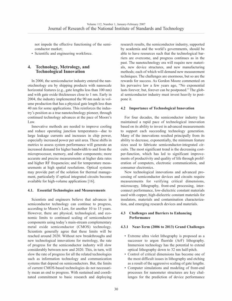
6. Appendix 1. Shorthand Notation Used in Table 1
This Appendix lists the page number and shorthand notation used in Table 1 for each of the 14 semiconductor casestudies of measurement needs appearing in Appendix B of Reference 1.
Case Study of Measurement Need - Page Number Shorthand NotationTechnology at Issue in Appendix B Used in Table 1
of Reference 1
In-line Inspection and Factory Control Equipment 204 Control
In-line/Real-time Analytic Tools for Measuring 205 Detectionand Detecting Sub-10 nm Defects
Dopant Distribution Instrumentation 206 Distributions
Interfacial Characterization Instrumentation 207 Interfaces
3D Atomic Mapping Instrumentation - Structural and 208 3D MappingMaterials Properties
Next-generation optical microscopes 209 Microscopes
Atomic Mapping Instrumentation - Light Elements 210 Light Element Mapping
Compound Semiconductor Cluster Tools 211 III-V Cluster Tools
Full System-on-Chip for Wireless Communications 212 RF Isolation
Sub-10 nm SEM Metrology Tools 213 SEM
Sidewall Characterization Instrumentation 214 Sidewall
Spin Metrology Tools 215 Spin
Semiconductor industry defect metrology tools 216 X-Ray
Instrumentation for Measurement of 217 Electrical PropertiesElectrical Properties at the Nanoscale

7. References
[1] An Assessment of the United States Measurement System:Addressing Measurement Barriers to Accelerate Innovation,NIST Special Publication 1048, Gaithersburg, MD, January2007. This report is available for downloading athttp://usms.nist.gov/.
[2] Semiconductor Industry Association., The InternationalTechnology Roadmap for Semiconductors, 2005 edition.SEMATECH:Austin, TX, http://www.itrs.net/Links/2005ITRS/ExecSum2005.pdf and http://www.itrs.net/Links/2005ITRS/Metrology2005.pdf .
[3] International Electronics Manufacturing Initiative, TheInternational Electronics Manufacturing Initiative Roadmaps,2004 Edition, Herndon, VA, http://www.inemi.org, page 8.
[4] 16 November 2005 SIA Press Release, SIA Forecast: Chip SalesWill Surpass $300 Billion in 2008, http://www.sia-online.org/pre_release.cfm?ID=386, page 2
[5] 2005 SIA Annual Report, http://www.sia-online.org/downloads/SIA_AR_2005.pdf, page 1.
[6] 2005 SIA Annual Report, http://www.sia-online.org/downloads/SIA_AR_2005.pdf, page 14.
[7] 2006 SIA Annual Report, http://www.sia-online.org/downloads/SIA_AR_2006.pdf, page 9.
[8] 16 November 2005 SIA Press Release, SIA Forecast: Chip SalesWill Surpass $300 Billion in 2008, http://www.sia-online.org/pre_release.cfm?ID=386, page 1.
[9] 2006 July, http://www.sia-online.org/pre_release.cfm?ID=414.[10] P. H. Singer, Dramatic Gains in Performance on the Horizon,
editorial in Semiconductor International, Vol. 29, No. 8 (July29, 2006) p. 15.
[11] 2005 SIA Annual Report, http://www.sia-online.org/downloads/SIA_AR_2005.pdf, page 3.
[12] T. N. Jackson, Nature Materials 4, 581 (August 2005). Prof.Jackson attributes this quote to Gordon Moore.
[13] T. N. Jackson, Nature Materials 4, 581 (August 2005).[14] 2004 iNEMI Roadmap, http://www.inemi.org, page 1.[15] SEMI S2, http://webstore.ansi.org/ansidocstore/product.asp?
sku=SEMI+S2-0706[16] Optical Roadmaps, http://www.spie.org/web/meetings/pro
grams/am00/confs/4099.html, http://thor.inemi.org/webdownload/newsroom/apex2005/2005_ECWC_iNEMI_Opto_Versus_Copper.pdf,
[17] 2004 iNEMI Roadmap, http://www.inemi.org, Overview, page3.
[18] G. Tassey, NIST Planning Report 98-4, prepared by TechneconAnalytic Research, May 1998, private communication, January2006.
[19] 2005 ITRS Executive Summary, http://www.itrs.net/Links/2005ITRS/ExecSum2005.pdf, page 8.
[20] 2005 ITRS Metrology Chapter, http://www.itrs.net/Links/2005ITRS/Metrology2005.pdf
[21] 2005 ITRS Executive Summary, http://www.itrs.net/Links/2005ITRS/ExecSum2005.pdf, page 55.
[22] Gilbert Declerck, IMEC, moderator for the Evening PanelDiscussion at the International Electron Devices Meeting(IEDM) on Semiconductor Research and Development: Whowill do it and who will pay for it in 2010? in Technical Digestof International Electron Devices Meeting, Washington, D.C.(December 6, 2005).
[23] Charles J. Nuese, Research Needs vs. Funding for the ITRS.SRC Internal, Document, 13 October 2003.
[24] Lewis Terman, in presentation to the Institute of Electrical andElectronics Engineers (IEEE), Electron Devices SocietyAdministrative Committee Meeting (EDS Admin), Washington,D.C., 4 December 2005.
[25] 2006 SIA Annual Report, http://www.sia-online.org/downloads/SIA_AR_2006.pdf, page 13.
[26] 2005 SIA Annual Report, http://www.sia-online.org/downloads/SIA_AR_2005.pdf, page 36.
[27] http://www.sia-online.org/downloads/Rising_Chorus.pdf, page1.
[28] D. de Solla Price, Exponential Growth, Big Science, andSaturated Economy, Public Policy Conference, Williamsburg,VA, December 16, 1971 and Little Science, Big Science ... AndBeyond, Columbia University Press, New York, 1963, Chapters4, 7, and 9.
[29] IDC 2004 Report entitled Modeling and Simulation: The Returnon Investment in Materials Science, http://www.idc.com andhttp://www.accelrys.com/reference/whitepapers/pub_mod_sim.php
[30] 2005 SIA Annual Report, http://www.sia-online.org/downloads/SIA_AR_2005.pdf, page 15
About the author: Herbert S. Bennett is a theoreticalsolid-state physicist and an electronics engineer in theSemiconductor Electronics Division of the NISTElectronics and Electrical Engineering Laboratory.The National Institute of Standards and Technology isan agency of the Technology Administration, U.S.Department of Commerce.
Volume 112, Number 1, January-February 2007Journal of Research of the National Institute of Standards and Technology
38