Embed Size (px)
Citation preview

6.012 - Electronic Devices and Circuits
Lecture 1 - Introduction to Semiconductors - Outline
• Introductions/AnnouncementsHandouts: 1. General information, reading assignments (4 pages)
2. Syllabus3. Student info sheet (for tutorials, do/due in recitation tomorrow!) 4. Diagnostic exam (try it on-line) 5. Lecture 1
Rules and regulations (next foil)
• Why semiconductors, devices, circuits? • Mobile charge carriers in semiconductors
Crystal structures, bondingMobile holes and electrons Dopants and doping
• Silicon in thermal equilibriumGeneration/recombination; nopo product no , po given Nd, Na; n- and p-types
• Drift MobilityConductivity and resistivity Resistors (our first device)
Clif Fonstad, 9/10/09 Lecture 1 - Slide 1

Comments/Rules and expectations Recitations: They re-enforce lecture.
They present new material. They are very important.
Tutorials: They begin Monday, September 14. Assignments will be posted on website.
Homework: Very important for learning; do it!!
Cheating: What you turn in must be your own work. While it is OK to discuss problems with others, you shouldwork alone when preparing your solution.
Reading assignment (Lec. 1) Chapter 1 in text* Chapter 2 in text
* "Microelectronic Devices and Circuits" by Clifton Fonstad http://dspace.mit.edu/handle/1721.1/34219
Clif Fonstad, 9/10/09 Lecture 1 - Slide 2

SEMICONDUCTORS: Here, there, and everywhere!
• Computers, PDAs, laptops, Silicon (Si) MOSFETs, Integrated Circuits (ICs), anything “intelligent” CMOS, RAM, DRAM, flash memory cells
• Cell phones, pagers, WiFi Si ICs, GaAs FETs, BJTs • CD players, iPods AlGaAs and InGaP laser diodes, Si photodiodes • TV remotes, mobile terminals Light emitting diodes • Satellite dishes InGaAs MMICs • Optical fiber networks InGaAsP laser diodes, pin photodiodes • Traffic signals, car GaN LEDs (green, blue)
taillights, dashboards InGaAsP LEDs (red, amber) • Air bags Si MEMs, Si ICs
They are very important, especially to EECS types!! They also provide:
a good intellectual framework and foundation, and
a good vehicle and context with which
to learn about modeling physical processes, and
to begin to understand electronic circuit analysis and design.
Clif Fonstad, 9/10/09 Lecture 1 - Slide 3

Silicon: our default example and our main focus
Atomic no. 14
14 electrons in three shells: 2 ) 8 ) 4
i.e., 4 electrons in the outer "bonding" shell Silicon forms strong covalent bonds with 4 neighbors
Si bonding configuration Silicon crystal ("diamond" lattice)
Figure by MIT OpenCourseWare.
Silicon crystal ("diamond" lattice)
Clif Fonstad, 9/10/09 Lecture 1 - Slide 4

Intrinsic silicon - pure, perfect, R.T.:
Electron• All bonds filled at 0 K, po = no = 0 energy
Si -
+
Conductingstates
Eg E ≈ 1.1 eVg
Bondingstates
• At R. T., po = no = ni = 1010 cm-3 Density of electronenergy states
• Mobile holes (+) and mobile electrons (-) • Compare to ≈ 5 x 10²² Si atoms/cm3
Clif Fonstad, 9/10/09 Lecture 1 - Slide 5

Intrinsic Silicon: pure Si, perfect crystal All bonds are filled at 0 K. At finite T, ni(T) bonds are broken:
!
Filled bond " Conduction electron + Hole
A very dynamic process, with bonds breaking and holes and electrons recombining continuously. On average:
!
• Concentration of conduction electrons " n
• Concentration of conduction electrons " p
In thermal equilibrium:
• n = no • p = po
and no = po = ni(T)
The intrinsic carrier concentration, ni, is very sensitive to temperature, varying exponentially with 1/T:
In silicon at room temperature, 300 K:
!
ni(T)"T3 / 2
exp(#Eg /2kT)
A very importantnumber; learn it!!
!
ni(T) "1010
cm#3
In 6.012 we only "do" R.T.Clif Fonstad, 9/10/09 Lecture 1 - Slide 6

1010 cm-3 is a very small concentration and intrinsic Si is an insulator; we need to do something
Extrinsic Silicon: carefully chosen impurities (dopants) added
Column IV elements (C, Si, Ge, α-Sn)
Te52
Se34
S16
B5
Zn30
Cd48
Po84
P15
Hg80
As33
Ge32
Ga31
Bi83
Tl81
Pb82
In49
Sb51
Sn50
C6
N7
O8
Si14
Al13II
III IV V VI
Column V elements (N, P, As, Sb): too many bonding electrons → electrons easily freed to conduct (-q charge)
→ fixed ionized donors created (+q charge)
Clif Fonstad, 9/10/09 Lecture 1 - Slide 7

A column V atom replacing a silicon atom in the lattice:
+Sb
−
Electron energy
Ed
Ed ≈ 45 meV
• One more electron than needed for bonding. Density of electronenergy states• Easily freed to conduct at RT.
• Impurity is an electron "donor." • Mobile electron (-) and fixed donor (+); Nd
+ ≈ Nd. Clif Fonstad, 9/10/09 Lecture 1 - Slide 8

Extrinsic Silicon, cont.: carefully chosen impurities (dopants) added
Column IV elements (C, Si, Ge, α-Sn)
Te52
Se34
S16
B5
Zn30
Cd48
Po84
P15
Hg80
As33
Ge32
Ga31
Bi83
Tl81
Pb82
In49
Sb51
Sn50
C6
N7
O8
Si14
Al13II
III IV V VI
Column III elements (B, Al, Ga, In): too few bonding electrons → leaves holes that can conduct (+q charge)
→ fixed ionized acceptors created (-q charge)
Clif Fonstad, 9/10/09 Lecture 1 - Slide 9

A column III atom replacing a silicon atom in the lattice:
B -
+
Electron energy
Ea ≈ 45 mev
Ea
• One less electron than needed for bonding. Density of electronenergy states
• Bond easily filled leaving mobile hole; at RT. • Impurity is an electron "acceptor." • Mobile hole (+) and fixed acceptor (−); Na
− ≈ Na. Clif Fonstad, 9/10/09 Lecture 1 - Slide 10

Extrinsic Silicon: carefully chosen impurities (dopants) added
Column IV elements (C, Si, Ge, α-Sn)
Te52
Se34
S16
B5
Zn30
Cd48
Po84
P15
Hg80
As33
Ge32
Ga31
Bi83
Tl81
Pb82
In49
Sb51
Sn50
C6
N7
O8
Si14
Al13II
III IV V VI
Column V elements (N, P, As, Sb): too many bonding electrons → electrons easily freed to conduct (-q charge)
→ fixed ionized donors created (+q charge)
Column III elements (B, Al, Ga, In): too few bonding electrons → leaves holes that can conduct (+q charge)
→ fixed ionized acceptors created (-q charge) Clif Fonstad, 9/10/09 Lecture 1 - Slide 11

Extrinsic Silicon: What are no and po in "doped" Si?
Column V elements (P, As, Sb): "Donors"
!
• Concentration of donor atoms " Nd [cm-3
]
Column III elements (B, Ga): "Acceptors"
!
• Concentration of acceptor atoms " Na [cm
-3]
At room temperature, all donors and acceptors are ionized:
!
• Nd
+" Nd • N
a
-" Na
We want to know, "Given Nd and Na, what are no and po?"
Two unknowns, no and po, so we need two equations.
Clif Fonstad, 9/10/09 Lecture 1 - Slide 12

Extrinsic Silicon: Given Na and Nd, what are no and po?
Equation 1 - Charge conservation (the net charge is zero):
!
q(po " no + Nd
+" Na
") = 0 # q(po " no + Nd " Na )
First equation
Equation 2 - Law of Mass Action (the np product is constant in TE):
!
no po = ni
2(T) Second equation
Where does this last equation come from? The semiconductor is in internal turmoil, with bonds being broken and reformed continuously:
!
Completed bond " # $ Electron + Hole
We have generation:
!
Completed bond " # " Electron + Hole
occurring at a rate G [pairs/cm3-s]:
!
Generation rate, G = Gext + go(T) = Gext + gm (T)
m
"
Clif Fonstad, 9/10/09 Lecture 1 - Slide 13

And we have recombination:
!
Electron + Hole " # " Completed bond
occurring at a rate R [pairs/cm3-s]:
!
Recombination rate, R = no poro(T) = no po rm (T)
m
"
In general we have:
!
dn
dt=
dp
dt= G " R = Gext + gm (T)
m
# " n p rm (T)
m
#
In thermal equilibrium, dn/dt = 0, dp/dt = 0, n = no, p = po, and Gext = 0, so:
!
0 = G " R = gm (T)
m
# " no po rm (T)
m
# $ gm (T)
m
# = no po rm (T)
m
#
But, the balance happens on an even finer scale. The Principle of Detailed Balance tells us that each G-R path is in balance:
!
gm (T) = no po rm (T) for all m
This can only be true if nopo is constant at fixed temperature, so we must have:
!
no po = ni
2(T)
Clif Fonstad, 9/10/09 Lecture 1 - Slide 14

Another way to get this result is to apply the Law of Mass Action from chemistry relating the concentrations of the reactants and products in a reaction in thermal equilibrium:
!
Electron[ ] Hole[ ] Completed bond[ ] = k(T)
!
Electron + Hole " # $ Completed bond
We know [Electron] = no and [Hole] = po, and recognizing that most of the bonds are still completed so [Completed bond] is essentially a constant*, we have
!
no po = [Completed bond] k(T) " A k(T) = ni
2(T)
Back to our question: Given N and Nd, what are n and p ?a o o
!
q(po " no + Nd
+" Na
") = 0 # q(po " no + Nd " Na )
First equation
Equation 1 - Charge conservation (the net charge is zero):
Equation 2 - Law of Mass Action (the np product is constant in TE):
!
no po = ni
2(T) Second equation
Clif Fonstad, 9/10/09 Lecture 1 - Slide 15* This requires that no and po be less than about 1019 cm-3.

!
ni
2
no
" no + Nd " Na
#
$ %
&
' ( = 0
no
2 " Nd " Na( )no " ni
2 = 0
Extrinsic Silicon, cont: Given Na and Nd, what are no and po?
Combine the two equations:
Solving for no we find:
!
no = Nd - Na( ) ± Nd - Na( )2
+ 4ni
2
2 =
Nd - Na( )2
1± 1+4ni
2
Nd - Na( )2
"
# $ $
%
& ' '
(Nd - Na( )
21± 1+
2ni
2
Nd - Na( )2
)
* + +
,
- . .
"
# $ $
%
& ' '
Note: Here we have used
!
1+ x " 1+ x 2 for x <<1
This expression simplifies nicely in the two cases we commonly encounter:
!
Case I - n - type : Nd > Na and Nd " Na( ) >> ni
Case II - p - type : Na > Nd and Na " Nd( ) >> ni
Fact of life: It is almost impossible to find a situationwhich is not covered by one of these two cases.
Clif Fonstad, 9/10/09 Lecture 1 - Slide 16

Extrinsic Silicon, cont.: solutions in Cases I and II
Case I - n-type: Nd > Na:, (Nd - Na) >> ni "n-type Si"
Define the net donor concentration, ND:
!
ND " (Nd # Na )
We find:
In Case I the concentration of electrons is much greater than that of holes. Silicon with net donors is called "n-type".
Case II - p-type: Na > Nd:, (Na - Nd) >> ni "p-type Si"
!
no " ND, po = ni
2(T) /no " ni
2(T) /ND
Define the net acceptor concentration, NA:
!
NA " (Na # Nd )
We find:
!
po " NA , no = ni
2(T) / po " ni
2(T) /NA
In Case II the concentration of holes is much greater than that of electrons. Silicon with net acceptors is called "p-type".
Clif Fonstad, 9/10/09 Lecture 1 - Slide 17

Uniform material with uniform excitations (pushing semiconductors out of thermal equilibrium)
A. Uniform Electric Field, Ex Drift motion:
Holes and electrons acquire a constant net velocity, sx,proportional to the electric field: No field E-field applied
εx
sex = "µe Ex, shx = µh Ex
�x
No field E-field applied
Figure by MIT OpenCourseWare.
At low and moderate |E|, the mobility, µ, is constant. At high |E| the velocity saturates and µ deceases with
increasing |E|. Clif Fonstad, 9/10/09 Lecture 1 - Slide 18

Uniform material with uniform excitations (pushing semiconductors out of thermal equilibrium)
A. Uniform Electric Field, Ex , cont. Drift motion:
Holes and electrons acquire a constant net velocity, sx,proportional to the electric field:
!
sex = "µe Ex, shx = µh Ex
At low and moderate |E|, the mobility, µ, is constant. At high |E| the velocity saturates and µ deceases.
Drift currents: Net velocities imply net charge flows, which imply currents:
!
Jex
dr = "q no sex = qµenoEx Jhx
dr = q po shx = qµh poEx
Note: Even though the semiconductor is no longer in thermalequilibrium the hole and electron populations still have theirthermal equilibrium values.
Clif Fonstad, 9/10/09 Lecture 1 - Slide 19

Velocity saturation The breakdown of Ohm's law at large electric fields.
102 105
106
107
108
103 104 105 106
Car
rier d
rift v
eloc
ity (c
m/s
)
Electric field (V/cm)
Ge
Si
GaAs (electrons)
T = 300K Electrons Holes
Figure by MIT OpenCourseWare.
Clif Fonstad, 9/10/09
Silicon
Above: Velocity vs. field plot at R.T. for holes and electrons in Si (log-logplot). (Fonstad, Fig. 3.2)
Left: Velocity-field curves for Si, Ge, and GaAs at R.T. (log-log plot). (Neaman, Fig. 5.7)
Lecture 1 - Slide 20

Conductivity, σo: Ohm's law on a microscale states that the drift current density islinearly proportional to the electric field:
!
Jx
dr =" o Ex
The total drift current is the sum of the hole and electron drift currents. Using our early expressions we find:
!
Jx
dr = Jex
dr + Jhx
dr = qµenoEx + qµh poEx = q µeno +µh po( )Ex
From this we see obtain our expression for the conductivity:
!
" o = q µeno +µh po( ) [S/cm]
Majority vs. minority carriers: Drift and conductivity are dominated by the most numerous, or"majority," carriers:
n-type
p-type
!
no >> po "# o $ qµeno
po >> no "# o $ qµh po
Clif Fonstad, 9/10/09 Lecture 1 - Slide 21

Resistance, R, and resistivity, ρo:
+ iD
Ohm's law on a macroscopic scale says that the current and
!
vab = R iD
σο
−voltage are linearly related: w
The question is, "What is R?" vAB t We have:
!
Jx
dr =" o Ex
with Ex =vAB
land Jx
dr =iD
w # t l
where
Note: Resistivity, ρo, is defined as the inverse of the conductivity:
Combining these we find:
!
iD
w " t=# o
vAB
l
!
vAB =l
w " t
1
# o
iD = R iD
R $l
w " t
1
# o
=l
w " t%o
which yields:
!
"o #1$ o
[Ohm - cm]
Clif Fonstad, 9/10/09 Lecture 1 - Slide 22

Integrated resistors Our first device!!
© Source unknown. All rights reserved. This content is excluded from our Creative Commons license. For more information, see http://ocw.mit.edu/fairuse.
Diffused resistors: High sheet resistance semiconductor patterns(pink) with low resistance Al (white) "wires" contacting each end.
© Source unknown. All rights reserved. This content is excluded from our Creative Commons license. For more information, see http://ocw.mit.edu/fairuse.
Thin-film resistors: High sheet resistance tantalum films (green)with low resistance Al (white) "wires" contacting each end.
Clif Fonstad, 9/10/09 Lecture 1 - Slide 23
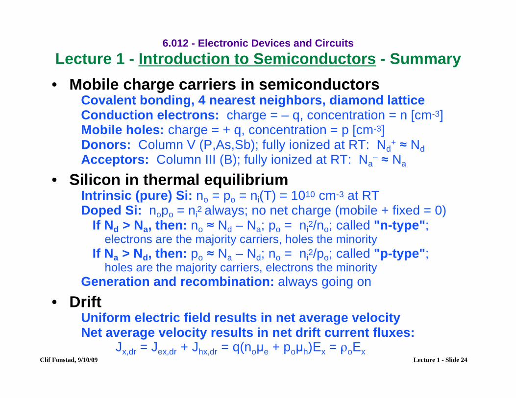
6.012 - Electronic Devices and Circuits
Lecture 1 - Introduction to Semiconductors - Summary
• Mobile charge carriers in semiconductorsCovalent bonding, 4 nearest neighbors, diamond lattice Conduction electrons: charge = – q, concentration = n [cm-3] Mobile holes: charge = + q, concentration = p [cm-3] Donors: Column V (P,As,Sb); fully ionized at RT: Nd
+ ≈ Nd –Acceptors: Column III (B); fully ionized at RT: Na ≈ Na
• Silicon in thermal equilibriumIntrinsic (pure) Si: no = po = ni(T) = 1010 cm-3 at RT Doped Si: nopo = ni2 always; no net charge (mobile + fixed = 0)
If Nd > Na, then: no ≈ Nd – Na; po = ni2/no; called "n-type"; electrons are the majority carriers, holes the minority
If Na > Nd, then: po ≈ Na – Nd; no = ni2/po; called "p-type"; holes are the majority carriers, electrons the minority
Generation and recombination: always going on • Drift
Uniform electric field results in net average velocity Net average velocity results in net drift current fluxes:
Jx,dr = Jex,dr + Jhx,dr = q(noµe + poµh)Ex = ρoEx Clif Fonstad, 9/10/09 Lecture 1 - Slide 24

MIT OpenCourseWarehttp://ocw.mit.edu
6.012 Microelectronic Devices and Circuits Fall 2009
For information about citing these materials or our Terms of Use, visit: http://ocw.mit.edu/terms.