Embed Size (px)
Citation preview
II. Basic Concepts of Semiconductor OE DevicesII. Basic Concepts of Semiconductor OE Devices
• Semiconductors– energy-band, bandgap energy, lattice constant– element & compound semiconductor– intrinsic & extrinsic semiconductor– direct & indirect semiconductor– carrier transport: Drift, Diffusion, Recombination, Generation– junction: p-n junction, M-S junction, Heterojunction, Multi-heterojunction,
Super-lattice, Quantum well
• Optoelectronics– OE materials: solid crystalline, non-crystalline– Optical spectrum– Luminescence– Electronic transition: radiative and non-radiative transition– Light Absorption and Emission
Optoelectronic Devices
Optoelectronics– the technology dealing with information processing with light
• Optoelectronic (Photonic) Devices– devices performing conversion between optical energy (photon) and electrical
energy• Electronic energy (singal) ⇔ Optical energy (signal or radiation)
• OE devices can be divided into three groups:– (1) Electronic energy ⇒ Radiation
• LED, Laser Diode (LD), EL devices, Display devices
– (2) Optical signal ⇒ Electrical signal
• Photodetectors
– (3) Optical radiation ⇒ Electrical energy
• Solar Cells
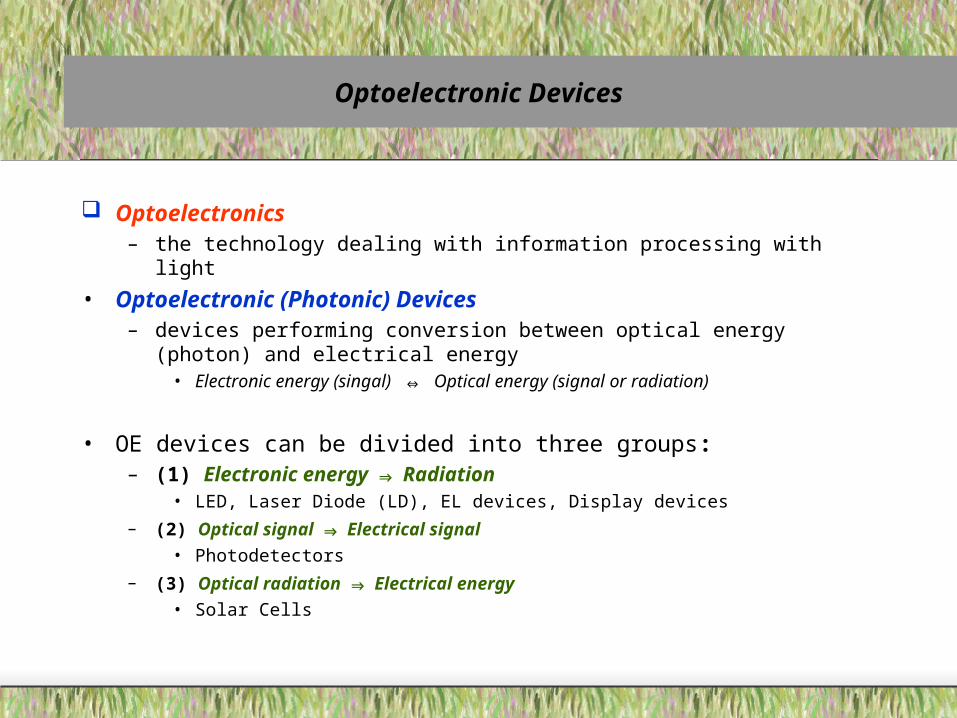
Applications of OE devices in modern technology Applications of OE devices in modern technology
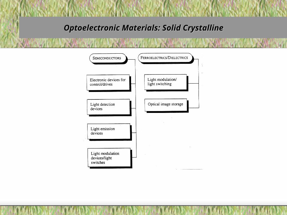
Optoelectronic Materials: Solid CrystallineOptoelectronic Materials: Solid Crystalline
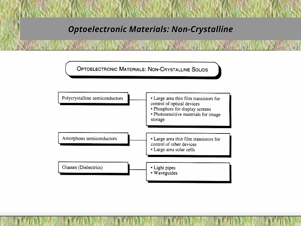
Optoelectronic Materials: Non-CrystallineOptoelectronic Materials: Non-Crystalline
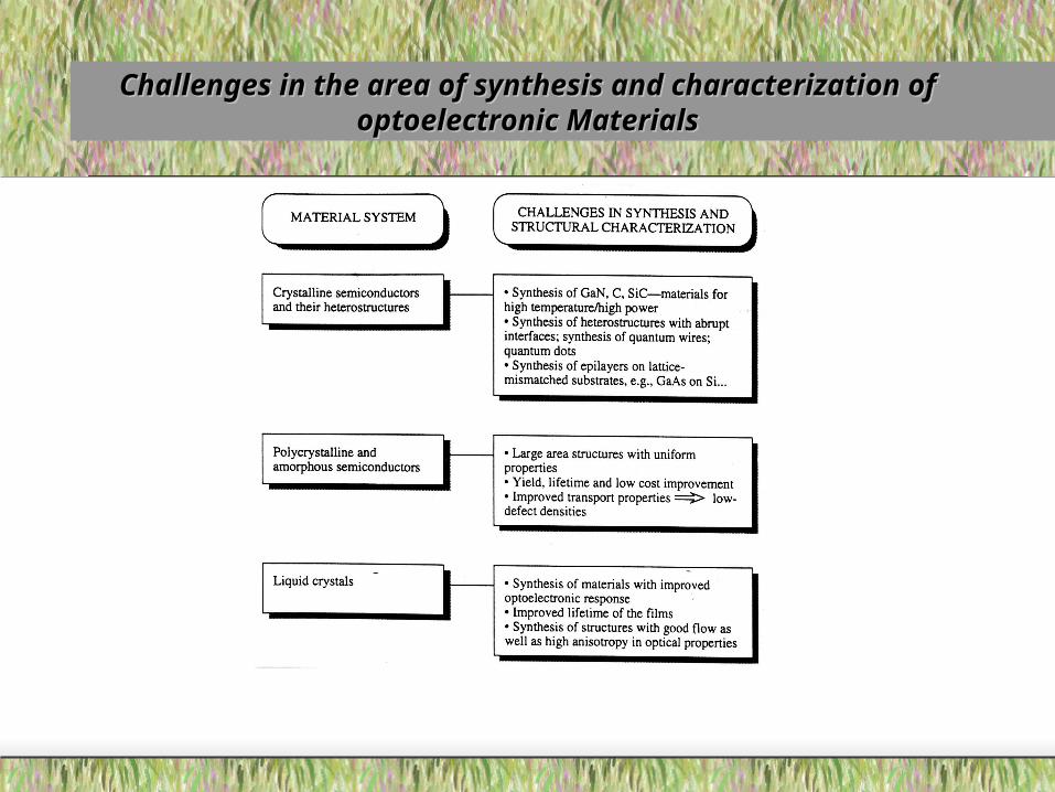
Challenges in the area of synthesis and characterization of Challenges in the area of synthesis and characterization of optoelectronic Materialsoptoelectronic Materials
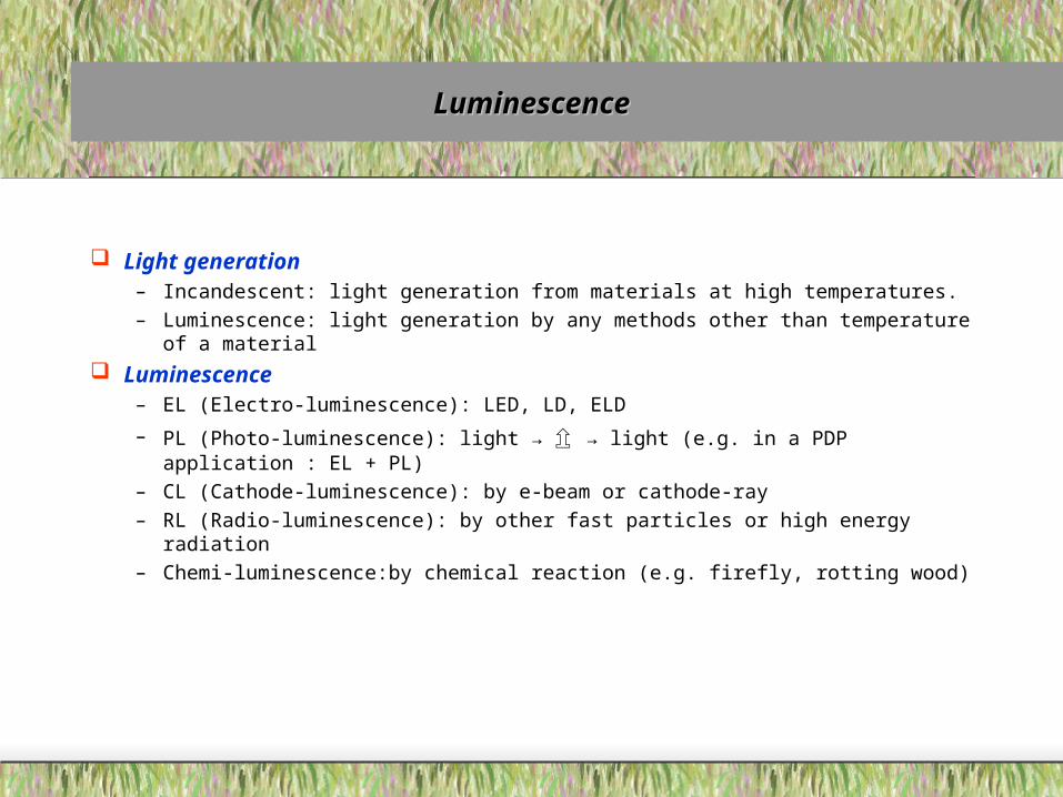
LuminescenceLuminescence
Light generation– Incandescent: light generation from materials at high temperatures.
– Luminescence: light generation by any methods other than temperature of a material
Luminescence– EL (Electro-luminescence): LED, LD, ELD
– PL (Photo-luminescence): light → ⇫ → light (e.g. in a PDP application : EL + PL)
– CL (Cathode-luminescence): by e-beam or cathode-ray
– RL (Radio-luminescence): by other fast particles or high energy radiation
– Chemi-luminescence:by chemical reaction (e.g. firefly, rotting wood)
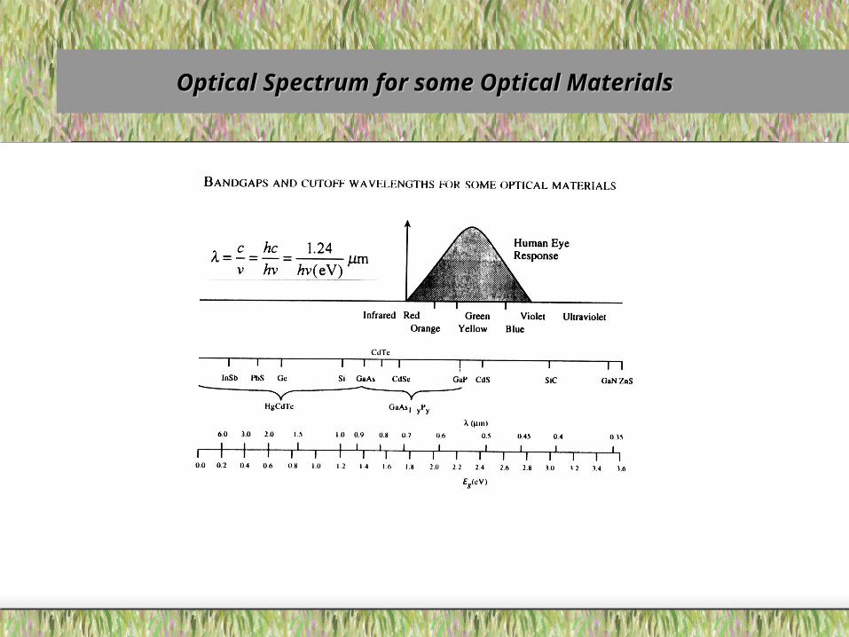
Optical Spectrum for some Optical MaterialsOptical Spectrum for some Optical Materials
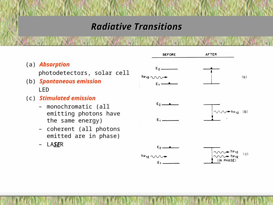
Radiative TransitionsRadiative Transitions
(a) Absorption
photodetectors, solar cell
(b) Spontaneous emission
LED
(c) Stimulated emission
– monochromatic (all emitting photons have the same energy)
– coherent (all photons emitted are in phase)
– LASER
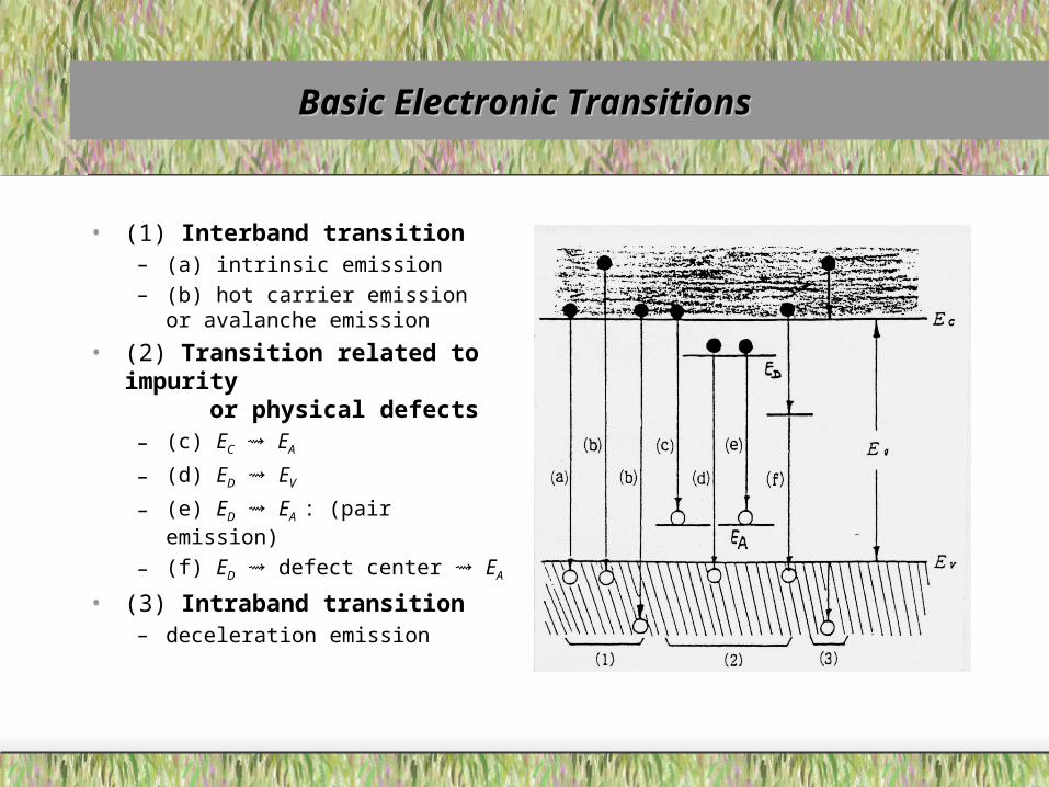
Basic Electronic TransitionsBasic Electronic Transitions
• (1) Interband transition– (a) intrinsic emission
– (b) hot carrier emission or avalanche emission
• (2) Transition related to impurity or physical defects
– (c) EC ⇝ EA
– (d) ED ⇝ EV
– (e) ED ⇝ EA : (pair emission)
– (f) ED ⇝ defect center ⇝ EA
• (3) Intraband transition– deceleration emission
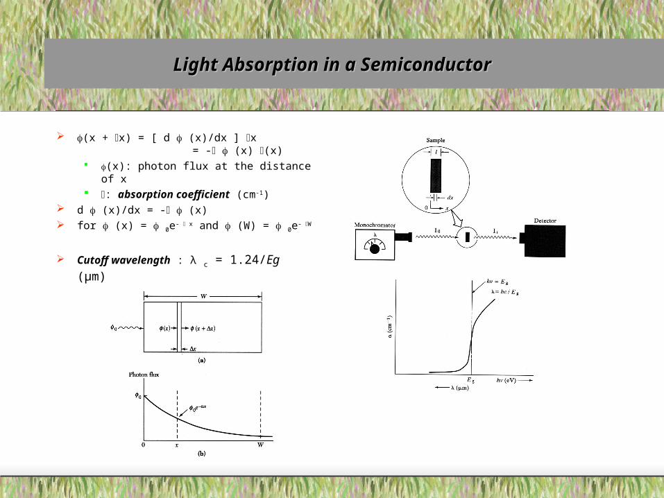
(x + x) = [ d (x)/dx ] x = - (x) (x)
(x): photon flux at the distance of x : absorption coefficient (cm-1)
d (x)/dx = - (x) for (x) = 0e- x and (W) = 0e- W
Cutoff wavelength : λ c = 1.24/Eg (μm)
Light Absorption in a SemiconductorLight Absorption in a Semiconductor
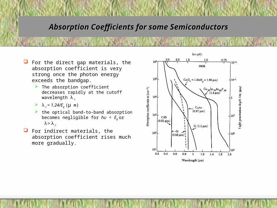
Absorption Coefficients for some SemiconductorsAbsorption Coefficients for some Semiconductors
For the direct gap materials, the absorption coefficient is very strong once the photon energy exceeds the bandgap. The absorption coefficient decreases
rapidly at the cutoff wavelength λ c
λ c = 1.24/Eg (μ m)
the optical band-to-band absorption becomes negligible for hυ < Eg or λ > λ c
For indirect materials, the absorption coefficient rises much more gradually.
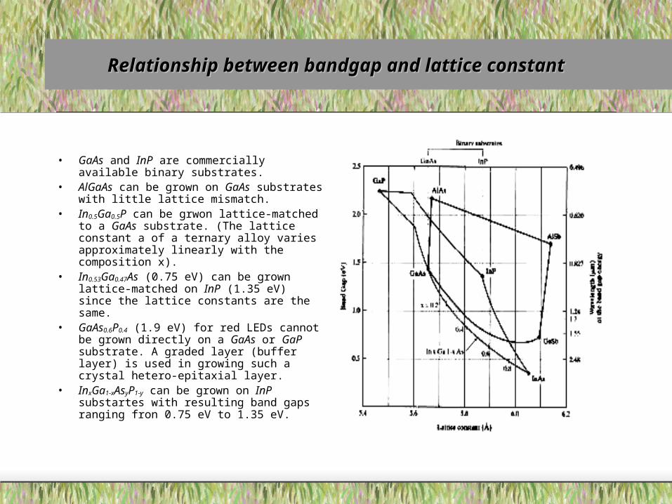
Relationship between bandgap and lattice constantRelationship between bandgap and lattice constant
• GaAs and InP are commercially available binary substrates.
• AlGaAs can be grown on GaAs substrates with little lattice mismatch.
• In0.5Ga0.5P can be grwon lattice-matched to a GaAs substrate. (The lattice constant a of a ternary alloy varies approximately linearly with the composition x).
• In0.53Ga0.47As (0.75 eV) can be grown lattice-matched on InP (1.35 eV) since the lattice constants are the same.
• GaAs0.6P0.4 (1.9 eV) for red LEDs cannot be grown directly on a GaAs or GaP substrate. A graded layer (buffer layer) is used in growing such a crystal hetero-epitaxial layer.
• InxGa1-xAsyP1-y can be grown on InP substartes with resulting band gaps ranging fron 0.75 eV to 1.35 eV.
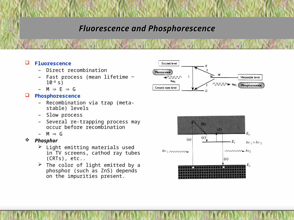
Fluorescence andFluorescence and PhosphorescencePhosphorescence
Fluorescence– Direct recombination– Fast process (mean lifetime ~ 10-8 s)– M E G
Phosphorescence– Recombination via trap (meta-stable)
levels– Slow process– Several re-trapping process may occur
before recombination – M G
Phosphor Light emitting materials used in TV
screens, cathod ray tubes (CRTs), etc.. The color of light emitted by a
phosphor (such as ZnS) depends on the impurities present.