Embed Size (px)
Citation preview
Dr. I. Manimehan, Department of Physics Mannai Rajagopalasamy Govt. Arts College, Mannargudi - 614001. Page 1
Unit – I Semiconductors, Diodes and Bipolar
transistors
Semiconductor
In terms of resistivity, it is a substance which has the resistivity in
between conductor and insulator.
Eg: Ge, Si
Energy Band:
The range of energies possessed by the electrons in a solid. There are
two important energy bands
1) Valance band 2) Conduction band
Valance Band:The range of energies possessed by the valance
electrons.
Conduction Band:The range of energies possessed by the conduction
electrons.
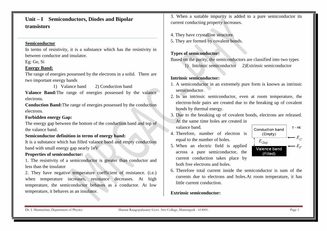
Forbidden energy Gap:
The energy gap between the bottom of the conduction band and top of
the valance band.
Semiconductor definition in terms of energy band:
It is a substance which has filled valance band and empty conduction
band with small energy gap nearly 1eV
Properties of semiconductor:
1. The resistivity of a semiconductor is greater than conductor and
less than the insulator
2. They have negative temperature coefficient of resistance. (i.e.)
when temperature increases, resistance decreases. At high
temperature, the semiconductor behaves as a conductor. At low
temperature, it behaves as an insulator.
3. When a suitable impurity is added to a pure semiconductor its
current conducting property increases.
4. They have crystalline structure.
5. They are formed by covalent bonds.
Types of semiconductor:
Based on the purity, the semiconductors are classified into two types
1) Intrinsic semiconductor 2)Extrinsic semiconductor
Intrinsic semiconductor:
1. A semiconductor in an extremely pure form is known as intrinsic
semiconductor.
2. In an intrinsic semiconductor, even at room temperature, the
electron-hole pairs are created due to the breaking up of covalent
bonds by thermal energy.
3. Due to the breaking up of covalent bonds, electrons are released.
At the same time holes are created in
valance band.
4. Therefore, number of electron is
equal to the number of holes.
5. When an electric field is applied
across a pure semiconductor, the
current conduction takes place by
both free electrons and holes.
6. Therefore total current inside the semiconductor is sum of the
currents due to electrons and holes.At room temperature, it has
little current conduction.
Extrinsic semiconductor:
Dr. I. Manimehan, Department of Physics Mannai Rajagopalasamy Govt. Arts College, Mannargudi - 614001. Page 2
1. At room temperature, intrinsic semiconductor has little current
conduction. So it must be altered to increase the current conducting
properties.
2. This is achieved by adding suitable impurity to a pure
semiconductor called extrinsic (or) impure (or) doped
semiconductor.
3. The purpose of adding impurities is to increase either the number
of electrons or holes.
4. Depending upon the type of impurity added, the extrinsic
semiconductors are classified into two types.
1. n type semiconductor 2. P type semiconductor
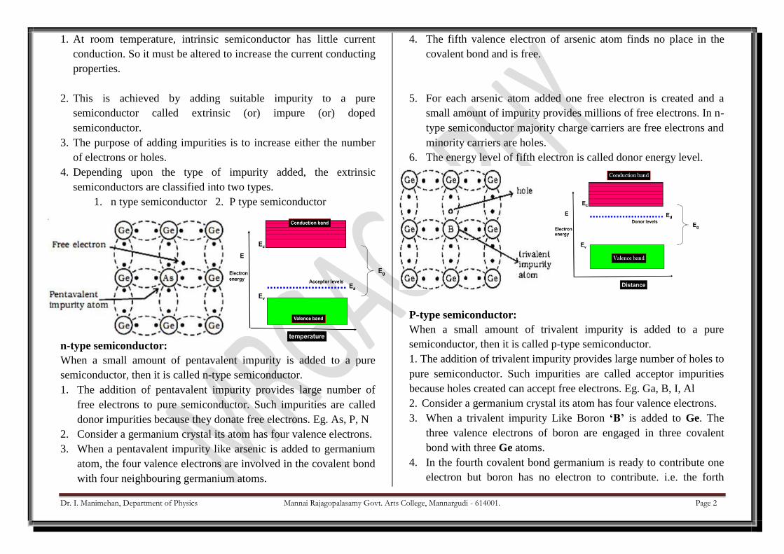
n-type semiconductor:
When a small amount of pentavalent impurity is added to a pure
semiconductor, then it is called n-type semiconductor.
1. The addition of pentavalent impurity provides large number of
free electrons to pure semiconductor. Such impurities are called
donor impurities because they donate free electrons. Eg. As, P, N
2. Consider a germanium crystal its atom has four valence electrons.
3. When a pentavalent impurity like arsenic is added to germanium
atom, the four valence electrons are involved in the covalent bond
with four neighbouring germanium atoms.
4. The fifth valence electron of arsenic atom finds no place in the
covalent bond and is free.
5. For each arsenic atom added one free electron is created and a
small amount of impurity provides millions of free electrons. In n-
type semiconductor majority charge carriers are free electrons and
minority carriers are holes.
6. The energy level of fifth electron is called donor energy level.
P-type semiconductor:
When a small amount of trivalent impurity is added to a pure
semiconductor, then it is called p-type semiconductor.
1. The addition of trivalent impurity provides large number of holes to
pure semiconductor. Such impurities are called acceptor impurities
because holes created can accept free electrons. Eg. Ga, B, I, Al
2. Consider a germanium crystal its atom has four valence electrons.
3. When a trivalent impurity Like Boron ‘B’ is added to Ge. The
three valence electrons of boron are engaged in three covalent
bond with three Ge atoms.
4. In the fourth covalent bond germanium is ready to contribute one
electron but boron has no electron to contribute. i.e. the forth

Dr. I. Manimehan, Department of Physics Mannai Rajagopalasamy Govt. Arts College, Mannargudi - 614001. Page 3
covalent bond is incomplete being shortage of one electron. The
missing electron is called a hole.
5. Each boron atom is added one hole is created and a small amount
of impurity provides millions of holes.
6. In p-type semiconductor majority charge carriers are holes and
minority charge carriers are free electrons.
DIFFERENCE BETWEEN INTRINSIC AND EXTRINSIC
SEMICONDUCTORS
Intrinsic Semiconductor Extrinsic Semiconductor
1) It is a pure form of semiconductor. It is an impure form of
semiconductor
2) At room temperature current
conducting property is low.
At room temperature current
conducting property is high.
3) Number of electrons are equal to
the number of holes.
Number of electron is not equal to the
number of holes.
4) The Fermi level lies between
valence band and conduction band.
In n-type , Fermi level lies between
donar energy level and conduction
band.
In p-type, Fermi level lies between
acceptor energy level and valence
band.
DIFFERENCE BETWEEN n-TYPE AND p-TYPE
SEMICONDUCTORS
PN junction Diode
When a p-type semiconductor is suitably joined to n-type semiconductor,
the contact surface is called PN junction. A pn junction is known as a semi-conductor or
*crystal diode. The outstanding property of pn
junction diode is to conduct current in one
direction. PN junction diode is usually
represented by the schematic symbol shown in Fig. The arrow in the symbol
indicates the direction of easier conventional current flow.
(i) If arrowhead of diode symbol is positive w.r.t. bar of the symbol, the
diode is forward biased.
(ii) If the arrowhead of diode symbol is negative w.r.t. bar, the diode is
reverse biased.
n-TYPE p-TYPE
1) It is formed by addition of
pentavalent impurity to pure
semiconductor.
It is formed by addition of trivalent
impurity to pure semiconductor.
2) Electrons are the majority carriers
and holes are the minority carriers.
Holes are the majority carriers and
electrons are the minority carriers
3) Fermi level lies between donor
energy level and conduction band.
Fermi level lies between the acceptor
level and valence band
4) When the temperature increases
the electrons moves from donor
energy level to conduction band.
When the temperature increases the
electrons moves from valence band
to acceptor energy level.
Dr. I. Manimehan, Department of Physics Mannai Rajagopalasamy Govt. Arts College, Mannargudi - 614001. Page 4
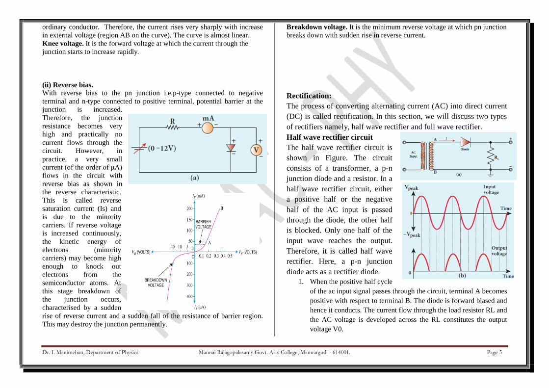
Depletion region (or Depletion layer). At the instant of pn-junction
formation, the free electrons
near the junction in the n
region begin to diffuse across
the junction into the p region
where they combine with holes
near the junction. The result is
that n region loses free
electrons as they diffuse into
the junction. This creates a
layer of positive charges near
the junction. Similarly the electrons move across the junction, the p
region loses holes as the electrons and holes combine. The result is that
there is a layer of negative charges near the junction. These two layers of
positive and negative charges form the depletion region (or depletion layer). Biasing of pn Junct ion
In electronics, the term bias refers to the use of d.c. voltage to establish
certain operating conditions for an electronic device. In relation to a pn
junction, there are following two bias conditions :
1. Forward biasing 2. Reverse biasing
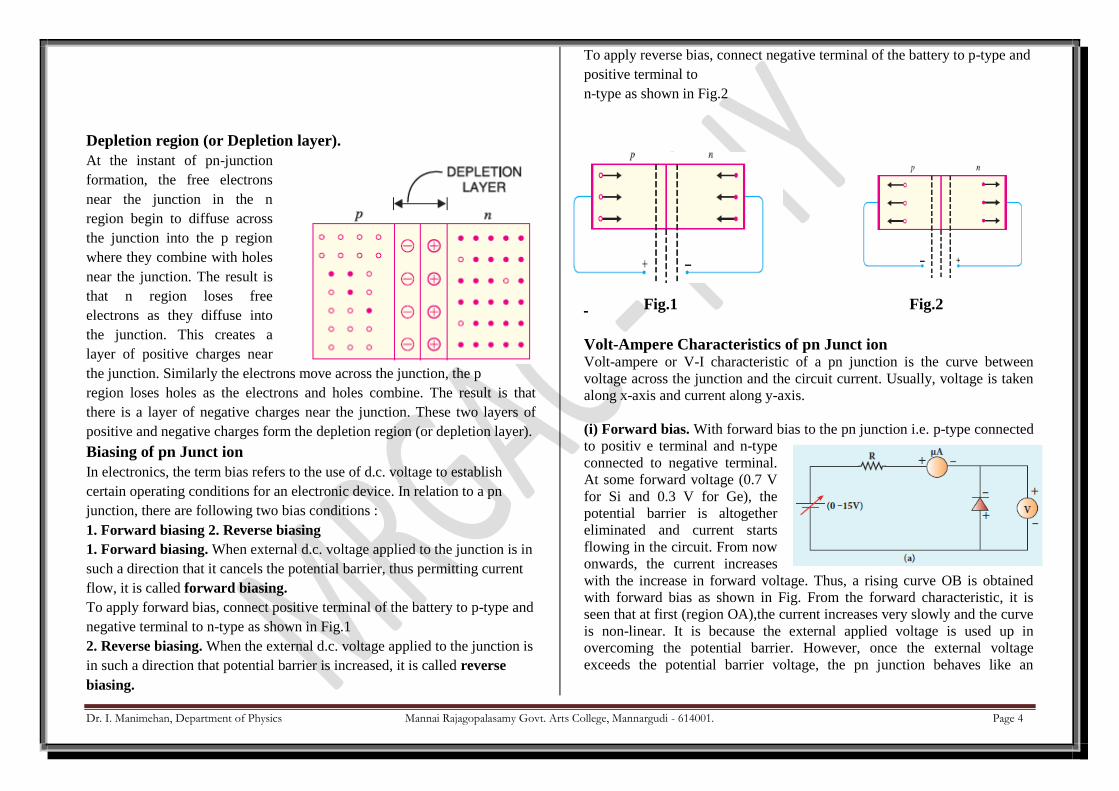
1. Forward biasing. When external d.c. voltage applied to the junction is in
such a direction that it cancels the potential barrier, thus permitting current
flow, it is called forward biasing.
To apply forward bias, connect positive terminal of the battery to p-type and
negative terminal to n-type as shown in Fig.1
2. Reverse biasing. When the external d.c. voltage applied to the junction is
in such a direction that potential barrier is increased, it is called reverse
biasing.
To apply reverse bias, connect negative terminal of the battery to p-type and
positive terminal to
n-type as shown in Fig.2
Fig.1 Fig.2
Volt-Ampere Characteristics of pn Junct ion Volt-ampere or V-I characteristic of a pn junction is the curve between
voltage across the junction and the circuit current. Usually, voltage is taken
along x-axis and current along y-axis.
(i) Forward bias. With forward bias to the pn junction i.e. p-type connected
to positiv e terminal and n-type
connected to negative terminal.
At some forward voltage (0.7 V
for Si and 0.3 V for Ge), the
potential barrier is altogether
eliminated and current starts
flowing in the circuit. From now
onwards, the current increases
with the increase in forward voltage. Thus, a rising curve OB is obtained
with forward bias as shown in Fig. From the forward characteristic, it is
seen that at first (region OA),the current increases very slowly and the curve
is non-linear. It is because the external applied voltage is used up in
overcoming the potential barrier. However, once the external voltage
exceeds the potential barrier voltage, the pn junction behaves like an
Dr. I. Manimehan, Department of Physics Mannai Rajagopalasamy Govt. Arts College, Mannargudi - 614001. Page 5
ordinary conductor. Therefore, the current rises very sharply with increase
in external voltage (region AB on the curve). The curve is almost linear.
Knee voltage. It is the forward voltage at which the current through the
junction starts to increase rapidly.
(ii) Reverse bias.
With reverse bias to the pn junction i.e.p-type connected to negative
terminal and n-type connected to positive terminal, potential barrier at the
junction is increased.
Therefore, the junction
resistance becomes very
high and practically no
current flows through the
circuit. However, in
practice, a very small
current (of the order of μA)
flows in the circuit with
reverse bias as shown in
the reverse characteristic.
This is called reverse
saturation current (Is) and
is due to the minority
carriers. If reverse voltage
is increased continuously,
the kinetic energy of
electrons (minority
carriers) may become high
enough to knock out
electrons from the
semiconductor atoms. At
this stage breakdown of
the junction occurs,
characterised by a sudden
rise of reverse current and a sudden fall of the resistance of barrier region.
This may destroy the junction permanently.
Breakdown voltage. It is the minimum reverse voltage at which pn junction
breaks down with sudden rise in reverse current.
Rectification:
The process of converting alternating current (AC) into direct current
(DC) is called rectification. In this section, we will discuss two types
of rectifiers namely, half wave rectifier and full wave rectifier.
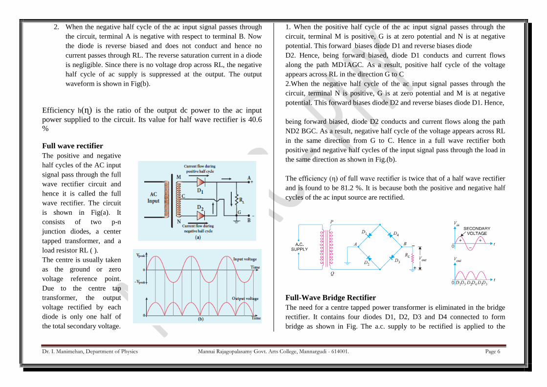
Half wave rectifier circuit
The half wave rectifier circuit is
shown in Figure. The circuit
consists of a transformer, a p-n
junction diode and a resistor. In a
half wave rectifier circuit, either
a positive half or the negative
half of the AC input is passed
through the diode, the other half
is blocked. Only one half of the
input wave reaches the output.
Therefore, it is called half wave
rectifier. Here, a p-n junction
diode acts as a rectifier diode.
1. When the positive half cycle
of the ac input signal passes through the circuit, terminal A becomes
positive with respect to terminal B. The diode is forward biased and
hence it conducts. The current flow through the load resistor RL and
the AC voltage is developed across the RL constitutes the output
voltage V0.
Dr. I. Manimehan, Department of Physics Mannai Rajagopalasamy Govt. Arts College, Mannargudi - 614001. Page 6
2. When the negative half cycle of the ac input signal passes through
the circuit, terminal A is negative with respect to terminal B. Now
the diode is reverse biased and does not conduct and hence no
current passes through RL. The reverse saturation current in a diode
is negligible. Since there is no voltage drop across RL, the negative
half cycle of ac supply is suppressed at the output. The output
waveform is shown in Fig(b).
Efficiency h(ɳ) is the ratio of the output dc power to the ac input
power supplied to the circuit. Its value for half wave rectifier is 40.6
%
Full wave rectifier
The positive and negative
half cycles of the AC input
signal pass through the full
wave rectifier circuit and
hence it is called the full
wave rectifier. The circuit
is shown in Fig(a). It
consists of two p-n
junction diodes, a center
tapped transformer, and a
load resistor RL ( ).
The centre is usually taken
as the ground or zero
voltage reference point.
Due to the centre tap
transformer, the output
voltage rectified by each
diode is only one half of
the total secondary voltage.
1. When the positive half cycle of the ac input signal passes through the
circuit, terminal M is positive, G is at zero potential and N is at negative
potential. This forward biases diode D1 and reverse biases diode
D2. Hence, being forward biased, diode D1 conducts and current flows
along the path MD1AGC. As a result, positive half cycle of the voltage
appears across RL in the direction G to C
2.When the negative half cycle of the ac input signal passes through the
circuit, terminal N is positive, G is at zero potential and M is at negative
potential. This forward biases diode D2 and reverse biases diode D1. Hence,
being forward biased, diode D2 conducts and current flows along the path
ND2 BGC. As a result, negative half cycle of the voltage appears across RL
in the same direction from G to C. Hence in a full wave rectifier both
positive and negative half cycles of the input signal pass through the load in
the same direction as shown in Fig.(b).
The efficiency (η) of full wave rectifier is twice that of a half wave rectifier
and is found to be 81.2 %. It is because both the positive and negative half
cycles of the ac input source are rectified.
Full-Wave Bridge Rectifier
The need for a centre tapped power transformer is eliminated in the bridge
rectifier. It contains four diodes D1, D2, D3 and D4 connected to form
bridge as shown in Fig. The a.c. supply to be rectified is applied to the
Dr. I. Manimehan, Department of Physics Mannai Rajagopalasamy Govt. Arts College, Mannargudi - 614001. Page 7
diagonally opposite ends of the bridge through the transformer. Between
other two ends of the bridge, the load resistance RL is connected.
1. During the positive half-cycle of secondary voltage, the end P of the
secondary winding becomes positive and end Q negative. This makes diodes
D1 and D3 forward biased while diodes D2 and D4 are reverse biased.
Therefore, only diodes D1 and D3 conduct. These two diodes will be in
series through the load RL. It may be seen that current flows from A to B
through the load RL .
2. During the negative half-cycle of secondary voltage, end P becomes
negative and end Q positive. This makes diodes D2 and D4 forward biased
whereas diodes D1 and D3 are reverse biased. Therefore, only diodes D2
and D4 conduct. These two diodes will be in series through the load RL. It
may be seen that again current flows from A to B through the load i.e. in the
same direction as for the positive half-cycle. Therefore, d.c. output is
obtained across load RL.
Breakdown mechanism
The reverse current or the reverse saturation current due to the
minority charge carriers is small. If the reverse bias applied to a p-n
junction is increased beyond a point, the junction breaks down and the
reverse current rises sharply. The voltage at which this happens is
called the breakdown voltage and it depends on the width of the
depletion region, which in turn depends on the doping level. There are
two mechanisms that are responsible for breakdown under increasing
reverse voltage.
Zener breakdown
Heavily doped p-n junctions have narrow depletion layers. When a reverse
voltage across this junction is increased to the breakdown limit, it rupture
the covalent bonds in the lattice and thereby generating electron-hole pairs.
This effect is called Zener effect.
Avalanche breakdown
Avalanche breakdown occurs in lightly doped junctions which have wide
depletion layers. Here, in this case, the electric field is not strong enough to
produce breakdown. Alternatively, the thermally generated minority charge
carriers accelerated by the electric field gains sufficient kinetic energy,
collide with the semiconductor atoms while
passing through the depletion region. This leads to the breaking of covalent
bonds and in turn generates electron-hole pairs.
ZENER DIODE
A zener diode is a special type of diode
that is designed to operate in the reverse
breakdown region. An ordinary diode
operated in this region will usually be
destroyed due to excessive current. This
is not the case for the zener diode.
A properly doped crystal diode which has a sharp breakdown voltage
is known as a zenerdiode. Fig.1 shows the symbol of a zener diode.
A zener diode is heavily
doped to reduce the reverse
breakdown voltage. This
causes a very thin depletion
layer. As a result, a zener
diode has a sharp reverse
breakdown voltage VZ. This is
clear from the reverse
characteristic of zener diode
Dr. I. Manimehan, Department of Physics Mannai Rajagopalasamy Govt. Arts College, Mannargudi - 614001. Page 8
shown in Fig. 2. Note that the reverse characteristic drops in an
almost vertical manner at reverse voltage VZ. As the curve reveals,
two things happen when VZ is reached :
The following points may be noted about the zener diode:
(i) A zener diode is like an ordinary diode except that it is properly
doped so as to have a sharp breakdown voltage.
(ii) A zener diode is always reverse connected i.e. it is always
reverse biased.
(iii) A zener diode has sharp breakdown voltagee, called zener
voltage VZ.
(iv) When forward biased, its characteristics are just those of
ordinary diode.
(v) The zener diode is not immediately burnt just because it has
entered the *breakdown region. As long as the external circuit
connected to the diode limits the diode current to less than
burn out value, the diode will not burn out.
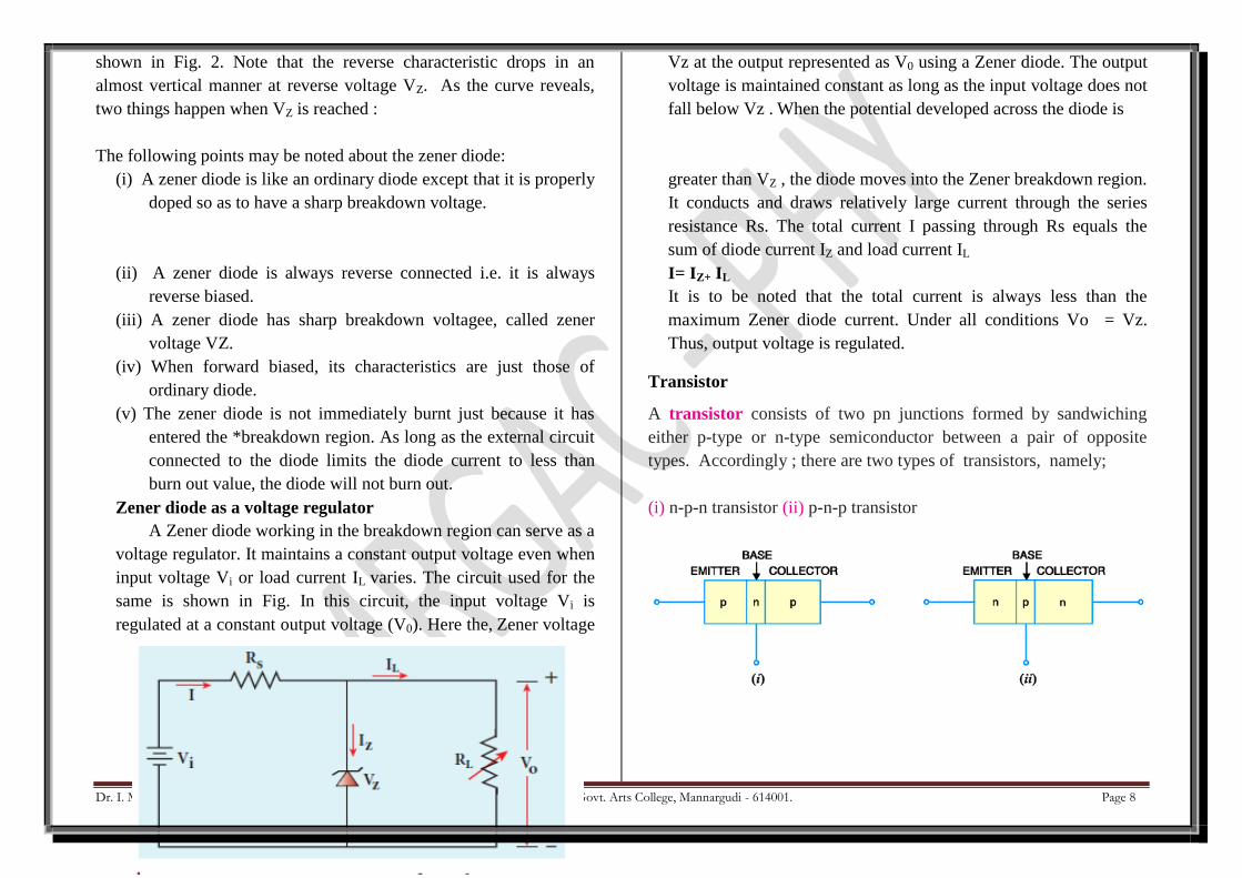
Zener diode as a voltage regulator
A Zener diode working in the breakdown region can serve as a
voltage regulator. It maintains a constant output voltage even when
input voltage Vi or load current IL varies. The circuit used for the
same is shown in Fig. In this circuit, the input voltage Vi is
regulated at a constant output voltage (V0). Here the, Zener voltage
Vz at the output represented as V0 using a Zener diode. The output
voltage is maintained constant as long as the input voltage does not
fall below Vz . When the potential developed across the diode is
greater than VZ , the diode moves into the Zener breakdown region.
It conducts and draws relatively large current through the series
resistance Rs. The total current I passing through Rs equals the
sum of diode current IZ and load current IL
I= IZ+ IL
It is to be noted that the total current is always less than the
maximum Zener diode current. Under all conditions Vo = Vz.
Thus, output voltage is regulated.
Transistor
A transistor consists of two pn junctions formed by sandwiching
either p-type or n-type semiconductor between a pair of opposite
types. Accordingly ; there are two types of transistors, namely;
(i) n-p-n transistor (ii) p-n-p transistor
Dr. I. Manimehan, Department of Physics Mannai Rajagopalasamy Govt. Arts College, Mannargudi - 614001. Page 9
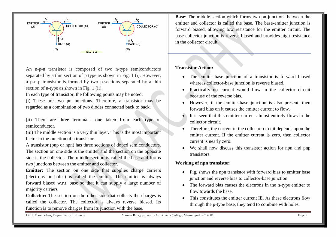
An n-p-n transistor is composed of two n-type semiconductors
separated by a thin section of p type as shown in Fig. 1 (i). However,
a p-n-p transistor is formed by two p-sections separated by a thin
section of n-type as shown in Fig. 1 (ii).
In each type of transistor, the following points may be noted:
(i) These are two pn junctions. Therefore, a transistor may be
regarded as a combination of two diodes connected back to back.
(ii) There are three terminals, one taken from each type of
semiconductor.
(iii) The middle section is a very thin layer. This is the most important
factor in the function of a transistor.
A transistor (pnp or npn) has three sections of doped semiconductors.
The section on one side is the emitter and the section on the opposite
side is the collector. The middle section is called the base and forms
two junctions between the emitter and collector.
Emitter: The section on one side that supplies charge carriers
(electrons or holes) is called the emitter. The emitter is always
forward biased w.r.t. base so that it can supply a large number of
majority carriers
Collector: The section on the other side that collects the charges is
called the collector. The collector is always reverse biased. Its
function is to remove charges from its junction with the base.
Base: The middle section which forms two pn-junctions between the
emitter and collector is called the base. The base-emitter junction is
forward biased, allowing low resistance for the emitter circuit. The
base-collector junction is reverse biased and provides high resistance
in the collector circuit.
Transistor Action:
The emitter-base junction of a transistor is forward biased
whereas collector-base junction is reverse biased.
Practically no current would flow in the collector circuit
because of the reverse bias.
However, if the emitter-base junction is also present, then
forward bias on it causes the emitter current to flow.
It is seen that this emitter current almost entirely flows in the
collector circuit.
Therefore, the current in the collector circuit depends upon the
emitter current. If the emitter current is zero, then collector
current is nearly zero.
We shall now discuss this transistor action for npn and pnp
transistors.
Working of npn transistor:
Fig. shows the npn transistor with forward bias to emitter base
junction and reverse bias to collector-base junction.
The forward bias causes the electrons in the n-type emitter to
flow towards the base.
This constitutes the emitter current IE. As these electrons flow
through the p-type base, they tend to combine with holes.
Dr. I. Manimehan, Department of Physics Mannai Rajagopalasamy Govt. Arts College, Mannargudi - 614001. Page 10
As the base is lightly doped and very thin, therefore, only a
few electrons (less than 5%) combine with holes to constitute
base current IB.
The remainder (more than 95%) cross over into the collector
region to constitute collector current IC.
In this way, almost the entire emitter current flows in the
collector circuit. It is clear that emitter current is the sum of
collector and base currents i.e.
IE = IB + IC
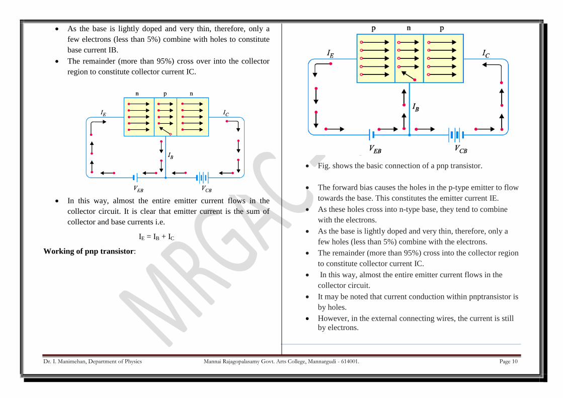
Working of pnp transistor:
Fig. shows the basic connection of a pnp transistor.
The forward bias causes the holes in the p-type emitter to flow
towards the base. This constitutes the emitter current IE.
As these holes cross into n-type base, they tend to combine
with the electrons.
As the base is lightly doped and very thin, therefore, only a
few holes (less than 5%) combine with the electrons.
The remainder (more than 95%) cross into the collector region
to constitute collector current IC.
In this way, almost the entire emitter current flows in the
collector circuit.
It may be noted that current conduction within pnptransistor is
by holes.
However, in the external connecting wires, the current is still
by electrons.
Dr. I. Manimehan, Department of Physics Mannai Rajagopalasamy Govt. Arts College, Mannargudi - 614001. Page 11
Transistor Connections:
1. There are three leads in a transistor viz., emitter, base and
collector terminals.
2. However, when a transistor is to be connected in a circuit, we
require four terminals; two for the input and two for the
output.
3. This difficulty is overcome by making one terminal of the
transistor common to both input and output terminals.
4. The input is fed between this common terminal and one of the
other two terminals.
5. The output is obtained between the common terminal and the
remaining terminal. Accordingly; a transistor can be
connected in a circuit in the following three ways
(i)
(ii) (i) Common base connection
(ii) Common emitter connection
(iii) Common collector connection
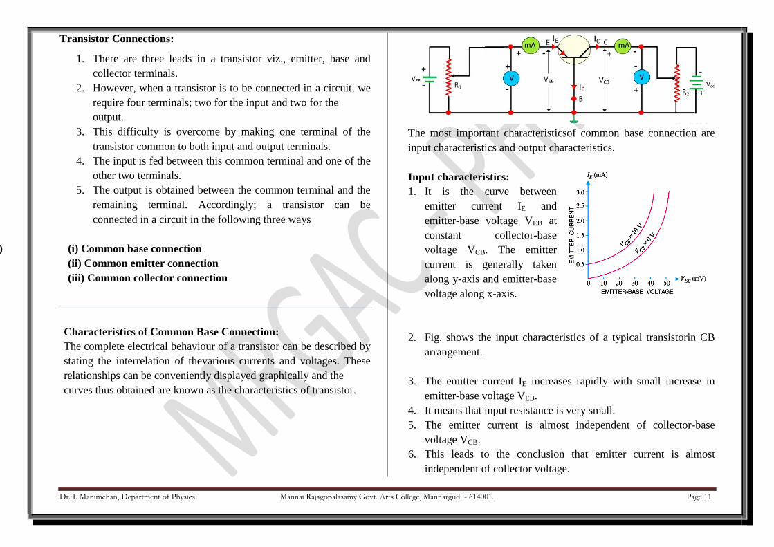
Characteristics of Common Base Connection:
The complete electrical behaviour of a transistor can be described by
stating the interrelation of thevarious currents and voltages. These
relationships can be conveniently displayed graphically and the
curves thus obtained are known as the characteristics of transistor.
The most important characteristicsof common base connection are
input characteristics and output characteristics.
Input characteristics:
1. It is the curve between
emitter current IE and
emitter-base voltage VEB at
constant collector-base
voltage VCB. The emitter
current is generally taken
along y-axis and emitter-base
voltage along x-axis.
2. Fig. shows the input characteristics of a typical transistorin CB
arrangement.
3. The emitter current IE increases rapidly with small increase in
emitter-base voltage VEB.
4. It means that input resistance is very small.
5. The emitter current is almost independent of collector-base
voltage VCB.
6. This leads to the conclusion that emitter current is almost
independent of collector voltage.
Dr. I. Manimehan, Department of Physics Mannai Rajagopalasamy Govt. Arts College, Mannargudi - 614001. Page 12
7. Input resistance. It is the ratio of changein emitter-base voltage
(ΔVEB) to the resultingchange in emitter current (ΔIE) at constant
collector-base voltage (VCB) i.e.
Input resistance, 𝒓𝒊 =∆𝑽𝑬𝑩
∆𝑰𝑬at constant VCB
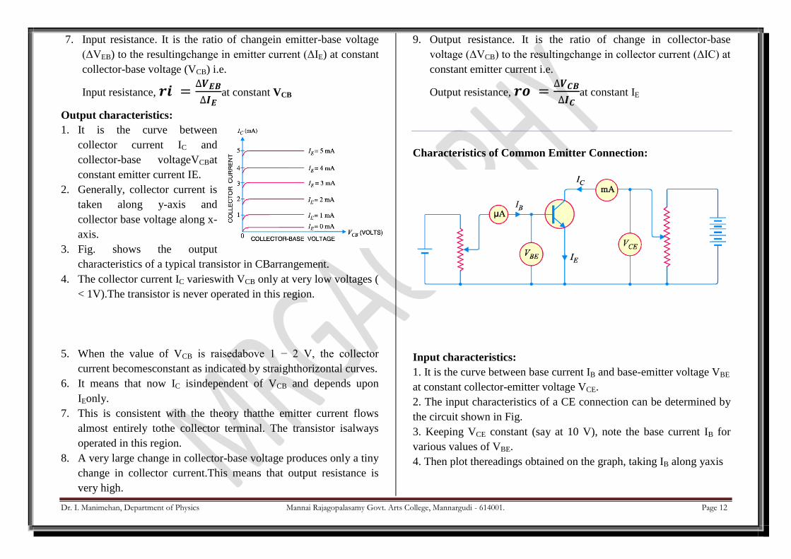
Output characteristics:
1. It is the curve between
collector current IC and
collector-base voltageVCBat
constant emitter current IE.
2. Generally, collector current is
taken along y-axis and
collector base voltage along x-
axis.
3. Fig. shows the output
characteristics of a typical transistor in CBarrangement.
4. The collector current IC varieswith VCB only at very low voltages (
< 1V).The transistor is never operated in this region.
5. When the value of VCB is raisedabove 1 − 2 V, the collector
current becomesconstant as indicated by straighthorizontal curves.
6. It means that now IC isindependent of VCB and depends upon
IEonly.
7. This is consistent with the theory thatthe emitter current flows
almost entirely tothe collector terminal. The transistor isalways
operated in this region.
8. A very large change in collector-base voltage produces only a tiny
change in collector current.This means that output resistance is
very high.
9. Output resistance. It is the ratio of change in collector-base
voltage (ΔVCB) to the resultingchange in collector current (ΔIC) at
constant emitter current i.e.
Output resistance, 𝒓𝒐 =∆𝑽𝑪𝑩
∆𝑰𝑪at constant IE
Characteristics of Common Emitter Connection:
Input characteristics:
1. It is the curve between base current IB and base-emitter voltage VBE
at constant collector-emitter voltage VCE.
2. The input characteristics of a CE connection can be determined by
the circuit shown in Fig.
3. Keeping VCE constant (say at 10 V), note the base current IB for
various values of VBE.
4. Then plot thereadings obtained on the graph, taking IB along yaxis
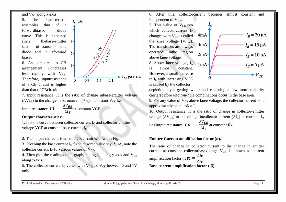
Dr. I. Manimehan, Department of Physics Mannai Rajagopalasamy Govt. Arts College, Mannargudi - 614001. Page 13
and VBE along x-axis.
5. The characteristic
resembles that of a
forwardbiased diode
curve. This is expected
since thebase-emitter
section of transistor is a
diode and it isforward
biased.
6. As compared to CB
arrangement, IBincreases
less rapidly with VBE.
Therefore, inputresistance
of a CE circuit is higher
than that of CBcircuit.
7. Input resistance. It is the ratio of change inbase-emitter voltage
(ΔVBE) to the change in basecurrent (ΔIB) at constant VCE i.e.
Input resistance, 𝒓𝒊 =∆𝑽𝑩𝑬
∆𝑰𝑩 at constant VCE
Output characteristics:
1. It is the curve between collector current IC and collector-emitter
voltage VCE at constant base current IB.
2. The output characteristics of a CE circuit isshown in Fig.
3. Keeping the base current IB fixed at some value say, 5 μA, note the
collector current IC forvarious values of VCE.
4. Then plot the readings on a graph, taking IC along y-axis and VCE
along x-axis.
5. The collector current IC varies with VCE,for VCE between 0 and 1V
only.
6. After this, collectorcurrent becomes almost constant and
independent of VCE.
7. This value of VCEupto
which collectorcurrent IC
changes with VCE is called
the knee voltage (Vknee).
The transistors are always
operated inthe region
above knee voltage.
8. Above knee voltage, IC
is almost constant.
However, a small increase
in IC with increasing VCE
is caused by the collector
depletion layer getting wider and capturing a few more majority
carriersbefore electron-hole combinations occur in the base area.
9. For any value of VCE above knee voltage, the collector current IC is
approximately equal toβ × IB.
10. Output resistance. It is the ratio of change in collector-emitter
voltage (ΔVCE) to the change incollector current (ΔIC) at constant IB
i.e.Output resistance, 𝒓𝒐 =∆𝑽𝑪𝑬
∆𝑰𝑪 at constant IB
Emitter Current amplification factor (𝛂).
The ratio of change in collector current to the change in emitter
current at constant collectorbasevoltage VCB is known as current
amplification factor i.e𝛂 =∆𝐈𝐂
∆𝐈𝑬
Base current amplification factor ( 𝛃).
Dr. I. Manimehan, Department of Physics Mannai Rajagopalasamy Govt. Arts College, Mannargudi - 614001. Page 14
The ratio of change in collector current (ΔIC) to the change in base
current (ΔIB) is known as base current amplification factor
i.e. 𝛃 =∆𝐈𝐂
∆𝐈𝐁
Relation between β and α.
A simple relation exists between β and α. This can be derived as
follows
β =∆IC
∆IB ---------- (1)
α =∆IC
∆I𝐸----------(2)
we know that
𝐼𝐸 = 𝐼𝐵 + 𝐼𝐶
∆𝐼𝐸 = ∆𝐼𝐵 + ∆𝐼𝐶
∆𝐼𝐵 = ∆𝐼𝐸 − ∆𝐼𝐶 ------------ (3)
Substituting the value of ΔIB in eqn. (1), we get
β =∆IC
∆𝐼𝐸 − ∆𝐼𝐶
Dividing the numerator and denominator of R.H.S. of eqn. (3) by ΔIE,
we get,
β =∆IC ∆𝐼𝐸
∆𝐼𝐸 − ∆𝐼𝐶 ∆𝐼𝐸
𝛃 =𝛂
𝟏 − 𝜷
It is clear that as α approaches unity, β approaches infinity
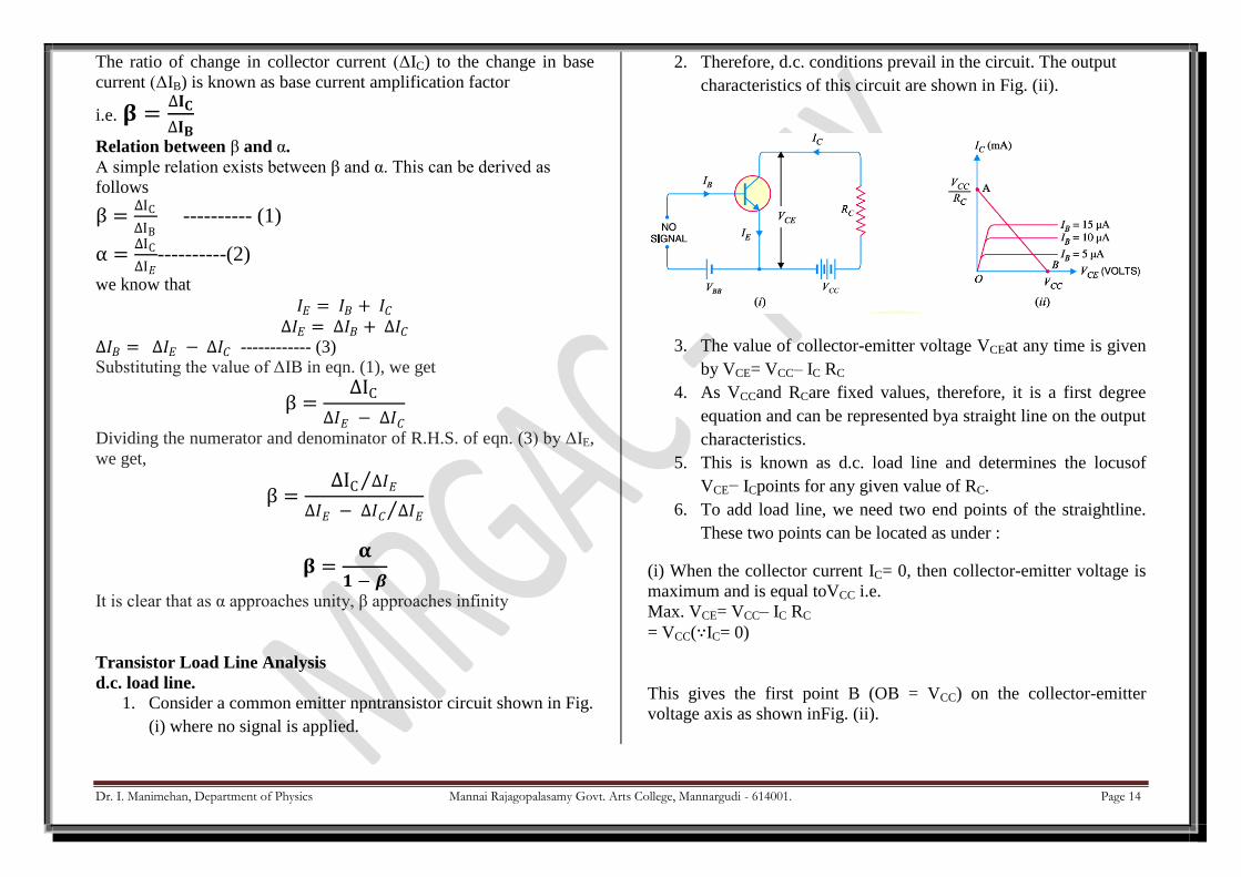
Transistor Load Line Analysis
d.c. load line.
1. Consider a common emitter npntransistor circuit shown in Fig.
(i) where no signal is applied.
2. Therefore, d.c. conditions prevail in the circuit. The output
characteristics of this circuit are shown in Fig. (ii).
3. The value of collector-emitter voltage VCEat any time is given
by VCE= VCC– IC RC
4. As VCCand RCare fixed values, therefore, it is a first degree
equation and can be represented bya straight line on the output
characteristics.
5. This is known as d.c. load line and determines the locusof
VCE− ICpoints for any given value of RC.
6. To add load line, we need two end points of the straightline.
These two points can be located as under :
(i) When the collector current IC= 0, then collector-emitter voltage is
maximum and is equal toVCC i.e.
Max. VCE= VCC– IC RC
= VCC(∵IC= 0)
This gives the first point B (OB = VCC) on the collector-emitter
voltage axis as shown inFig. (ii).
Dr. I. Manimehan, Department of Physics Mannai Rajagopalasamy Govt. Arts College, Mannargudi - 614001. Page 15
(ii) When collector-emitter voltage VCE = 0, the collector current is
maximum and is equal toVCC /RC i.e.
VCE= VCC− IC RC
or 0 = VCC− IC RC
∴ Max.IC= VCC/RC
This gives the second point A (OA = VCC /RC) on
the collector current axis as shown in Fig. (ii).
By joining these two points, d.c. *load line AB is
constructed.
Transistor Biasing:
The proper flow of zero signal collector current and the maintenance
of proper collector-emittervoltage during the passage of signal is
known as transistor biasing.
Stabilization:
The process of making operating point independent of temperature
changes or variations intransistor parameters is known as
stabilization.
Methods of Transistor Biasing
In the transistor amplifier circuits drawn so far biasing was done with
the aid of a battery VBB whichwas separate from the battery VCC
used in the output circuit. However, in the interest of simplicity
and economy, it is desirable that transistor circuit should have a single
source of supply—the one inthe output circuit (i.e. VCC). The
following are the most commonly used methods of obtaining
transistorbiasing from one source of supply (i.e. VCC ) :
(i) Base resistor method or fixed bias
(ii) Emitter bias method
(iii) Biasing with collector-feedback
resistor
(iv) Voltage-divider bias
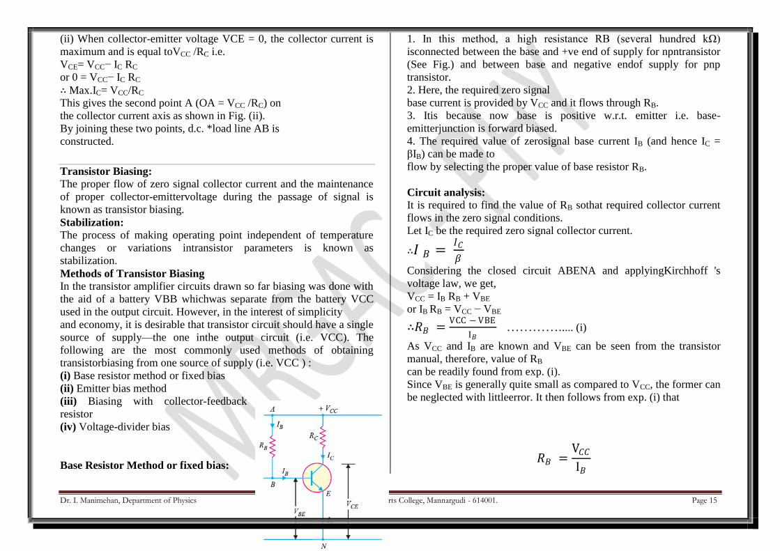
Base Resistor Method or fixed bias:
1. In this method, a high resistance RB (several hundred kΩ)
isconnected between the base and +ve end of supply for npntransistor
(See Fig.) and between base and negative endof supply for pnp
transistor.
2. Here, the required zero signal
base current is provided by VCC and it flows through RB.
3. Itis because now base is positive w.r.t. emitter i.e. base-
emitterjunction is forward biased.
4. The required value of zerosignal base current IB (and hence IC =
βIB) can be made to
flow by selecting the proper value of base resistor RB.
Circuit analysis:
It is required to find the value of RB sothat required collector current
flows in the zero signal conditions.
Let IC be the required zero signal collector current.
∴𝐼 𝐵 = 𝐼𝐶
𝛽
Considering the closed circuit ABENA and applyingKirchhoff 's
voltage law, we get,
VCC = IB RB + VBE
or IB RB = VCC − VBE
∴𝑅𝐵 =VCC − VBE
I𝐵 …………..... (i)
As VCC and IB are known and VBE can be seen from the transistor
manual, therefore, value of RB
can be readily found from exp. (i).
Since VBE is generally quite small as compared to VCC, the former can
be neglected with littleerror. It then follows from exp. (i) that
𝑅𝐵 =V𝐶𝐶
I𝐵
Dr. I. Manimehan, Department of Physics Mannai Rajagopalasamy Govt. Arts College, Mannargudi - 614001. Page 16
It may be noted that VCC is a fixed known quantity and IB is chosen at
some suitable value. Hence,RBcan always be found directly, and for
this reason, this method is sometimes called fixed-bias method.
Advantages :
(i) This biasing circuit is very simple as only one resistance RB is
required.
(ii) Biasing conditions can easily be set and the calculations are
simple.
(iii) There is no loading of the source by the biasing circuit since no
resistor is employed acrossbase-emitter junction.
Disadvantages :
(i) This method provides poor stabilisation. It is because there is no
means to stop a self-increasein collector current due to temperature
rise and individual variations. For example, if βincreases due to
transistor replacement, then IC also increases by the same factor as IB
is constant.
(ii) The stability factor is very high. Therefore, there are strong
chances of thermal runaway.Due to these disadvantages, this method
of biasing is rarely employed.
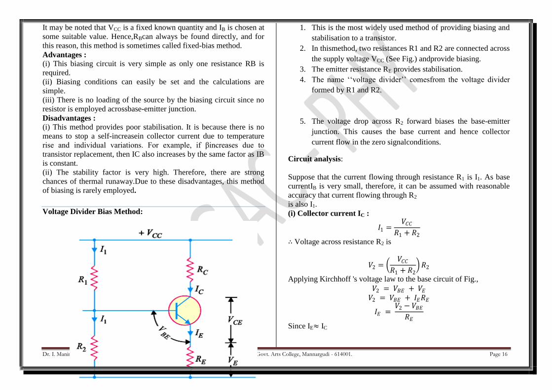
Voltage Divider Bias Method:
1. This is the most widely used method of providing biasing and
stabilisation to a transistor.
2. In thismethod, two resistances R1 and R2 are connected across
the supply voltage VCC (See Fig.) andprovide biasing.
3. The emitter resistance RE provides stabilisation.
4. The name ‘‘voltage divider’’ comesfrom the voltage divider
formed by R1 and R2.
5. The voltage drop across R2 forward biases the base-emitter
junction. This causes the base current and hence collector
current flow in the zero signalconditions.
Circuit analysis:
Suppose that the current flowing through resistance R1 is I1. As base
currentIB is very small, therefore, it can be assumed with reasonable
accuracy that current flowing through R2
is also I1.
(i) Collector current IC :
𝐼1 =𝑉𝐶𝐶
𝑅1 + 𝑅2
∴ Voltage across resistance R2 is
𝑉2 = 𝑉𝐶𝐶
𝑅1 + 𝑅2 𝑅2
Applying Kirchhoff 's voltage law to the base circuit of Fig.,
𝑉2 = 𝑉𝐵𝐸 + 𝑉𝐸
𝑉2 = 𝑉𝐵𝐸 + 𝐼𝐸𝑅𝐸
𝐼𝐸 = 𝑉2 − 𝑉𝐵𝐸
𝑅𝐸
Since IE≈ IC
Dr. I. Manimehan, Department of Physics Mannai Rajagopalasamy Govt. Arts College, Mannargudi - 614001. Page 17
𝐼𝐶 = 𝑉2−𝑉𝐵𝐸
𝑅𝐸...(i)
It is clear from exp. (i) above that IC does not at all depend upon β.
Though IC depends upon VBEbut in practice V2>> VBE so that IC is
practically independent of VBE. Thus IC in this circuit is almost
independent of transistor parameters and hence good stabilisation is
ensured. It is due to this reasonthat potential divider bias has become
universal method for providing transistor biasing.
(ii) Collector-emitter voltage VCE:
Applying Kirchhoff 's voltage law to the collector side,
VCC = IC RC + VCE + IE RE
= IC RC + VCE + IC RE (ä IE j IC)
= IC (RC + RE) + VCE
∴ VCE = VCC − IC (RC + RE)
Stabilisation: In this circuit, excellent stabilisation is provided by RE. Consideration
of eq. (i)reveals this fact.
V2 = VBE + IC RE
Suppose the collector current IC increases due to rise in temperature.
This will cause the voltagedrop across emitter resistance RE to
increase. As voltage drop across R2 (i.e. V2) isindependent of
IC, therefore, VBE decreases. This in turn causes IB to decrease. The
reduced value of IB tends torestore IC to the original value.


